ieee transactions on circuits and systems—i: · pdf fileieee transactions on circuits...
TRANSCRIPT

IEEE TRANSACTIONS ON CIRCUITS AND SYSTEMS—I: REGULAR PAPERS, VOL. 61, NO. 11, NOVEMBER 2014 3155
Energy/Reliability Trade-Offs in Low-VoltageReRAM-Based Non-Volatile Flip-Flop DesignIbrahim Kazi, Pascal Meinerzhagen, Member, IEEE, Pierre-Emmanuel Gaillardon, Member, IEEE,Davide Sacchetto, Member, IEEE, Yusuf Leblebici, Fellow, IEEE, Andreas Burg, Member, IEEE, and
Giovanni De Micheli, Fellow, IEEE
Abstract—The total power budget of Ultra-Low Power (ULP)VLSI Systems-on-Chip (SoCs) is often dominated by the leakagepower of embedded memories as well as status registers. Onthe one hand, supply voltage scaling down to the near-threshold(near- ) or even to the subthreshold (sub- ) domain is acommonly used, efficient technique to reduce both leakage powerand active energy dissipation. On the other hand, emergingCMOS-compatible device technologies such as Resistive Mem-ories (ReRAMs) enable non-volatile, on-chip data storage andzero-leakage sleep periods. For the first time, we present andcompare ReRAM-based Non-Volatile Flip-Flop (NVFF) topolo-gies which are optimized for low-voltage operation (includingnear- and sub- operation). Three low-voltage NVFF cir-cuit topologies are proposed and evaluated in terms of energydissipation and reliability. Using topologies with two comple-mentary programmed ReRAM devices, Monte Carlo simulationsaccounting for parametric variations confirm reliable data restoreoperation from the ReRAM devices at a sub- voltage as low as400 mV. A topology using a single ReRAM device exhibits lowerwrite energy, but requires a near- voltage for robust read.Energy characterization is performed at nominal, near- , andsub- supply voltages. The minimum energy point is reached fornear- read operation with a total read+write energy of 735 fJ.
Index Terms—Flip-flops, low-power electronics, nonvolatilememory.
I. INTRODUCTION
U LTRA-LOW POWER (ULP) VLSI systems such as wire-less sensor nodes [1] and biomedical implants [2], run-
ning for many days or even for several years on a single batterycharge, have extremely low power budgets. Embedded memo-
Manuscript received February 14, 2014; revised April 23, 2014; acceptedMay 26, 2014. Date of publication July 16, 2014; date of current versionOctober 24, 2014. This work was supported in part by the ERC senior grantNanoSys ERC-2009-AdG-246810 and the Swiss National Science Foundationunder the projects number PP002-119057 and number 200021-146600. Thework of P. Meinerzhagen was supported by an Intel Ph.D. fellowship. Thispaper was recommended by Associate Editor Corinto Fernando.I. Kazi, P.-E. Gaillardon, and G. De Micheli are with the Integrated Sys-
tems Laboratory (LSI), EPFL, Lausanne, VD, 1015 Switzerland (e-mail:[email protected]).P. Meinerzhagen was with the Telecommunications Circuits Labo-
ratory (TCL), EPFL, Lausanne, VD, 1015 Switzerland. He is nowwith Intel Labs, Intel Corporation, Hillsboro, OR 97124 USA (e-mail:[email protected]).D. Sacchetto is with the Integrated Systems Laboratory (LSI), EPFL, Lau-
sanne, VD, 1015 Switzerland. He is also with the Microelectronic Systems Lab-oratory (LSM), EPFL, Lausanne, VD, 1015 Switzerland.Y. Leblebici is with the Microelectronic Systems Laboratory (LSM), EPFL,
Lausanne, VD, 1015 Switzerland.A. Burg is with Telecommunications Circuits Laboratory (TCL), EPFL, Lau-
sanne, VD, 1015 Switzerland.Color versions of one or more of the figures in this paper are available online
at http://ieeexplore.ieee.org.Digital Object Identifier 10.1109/TCSI.2014.2334891
ries as well as status and pipeline registers consume a dominantshare of the total power and area of such systems [3], whilefor the digital signal processing core the share is often small.This power dominance of memories is further exacerbated forsystems with only short active computational periods and longsleep periods requiring data and program state retention. In suchcases, the leakage power of embedded memories and registersaccounts for almost the totality of the VLSI system’s powerconsumption.Supply voltage scaling to the near-threshold (near- )
regime or even down to the subthreshold (sub- ) regime isan efficient technique to reduce leakage power consumption(as well as active energy dissipation), at the cost of a speeddegradation and increased sensitivity to process parametervariations [4].While near- and sub- operation enables extremely
low leakage power, emerging device technologies allowingthe integration of non-volatile memory devices on top ofCMOS chips bear the potential of zero-leakage sleep states[5]. Among many technological options, Oxide Memories(OxRAMs) [6] are a promising candidate for next generationnon-volatile memory applications. Compared to traditionalFlash memories, OxRAMs have better scalability and fasterprogramming time [6]. While a lot of research effort targetsOxRAM-based stand-alone memories, this work focuses on theseamless integration of OxRAM devices into CMOS flip-flopsfor use as non-volatile, distributed storage elements. Previousworks on non-volatile flip-flops were based on the “memristor”[5], [7], on bipolar OxRAM [8], and Magnetic Tunneling Junc-tion (MTJ) devices [9]–[11]. All these works consider circuitoperation at a high supply voltage, normally corresponding tothe CMOS technology’s nominal voltage.In this work, we combine the advantages of an emerging non-
volatile memory device technology (namely, OxRAM stacks)with the assets of low-voltage (near- and sub- ) circuit op-eration by specifically optimizing the NVFF topologies for theseoperating regimes, thereby enabling future VLSI systems withultra-low active energy dissipation in addition to non-volatiledata storage with zero leakage. This article extends our previouswork [12] by introducing two new NVFF topologies and by pre-senting a detailed comparative analysis of all topologies.Our detailed, simulation-based analyses show that the state
of the art of NVFF design is extended on the following fronts:1) the NVFF topologies using two complementary programmedReRAM devices reliably recover the saved data on wake-upwith a sub- supply voltage and a standard deviation of up to5% of the nominal value of the ReRAM resistance; 2) in addi-tion, all proposed NVFF circuits are able to reliably recover data
1549-8328 © 2014 IEEE. Personal use is permitted, but republication/redistribution requires IEEE permission.See http://www.ieee.org/publications_standards/publications/rights/index.html for more information.
3156 IEEE TRANSACTIONS ON CIRCUITS AND SYSTEMS—I: REGULAR PAPERS, VOL. 61, NO. 11, NOVEMBER 2014
with a High Resistance Value (HRV) to Low Resistance Value(LRV) ratio of less than two, even though a near- voltage isrequired for the NVFF topology based on a single ReRAM de-vice to do so; and 3) thanks to circuit optimizations allowing foraggressive voltage scaling (down to the sub- domain for mostcircuits), the read energy has been drastically reduced to 5.4%of the total read+write energy, whereas for operation at nominalvoltage, read and write would have similar energy costs.The remainder of this paper is organized as follows. Section II
introduces the manufactured ReRAM stacks and elaborates ontheir switching behavior. Next, Section III introduces three fun-damentally different NVFF topologies based on one and twoReRAM devices and expatiates on their circuit-level optimiza-tions for reliable low-voltage operation. Section IV presents de-tailed circuit simulation results of all NVFF topologies and com-pares their read robustness as well as their read and write energyat nominal, near- , and sub- supply voltages, and Section Vconcludes this paper.
II. RESISTIVE MEMORY: MANUFACTURING PROCESS ANDSWITCHING CHARACTERISTICS
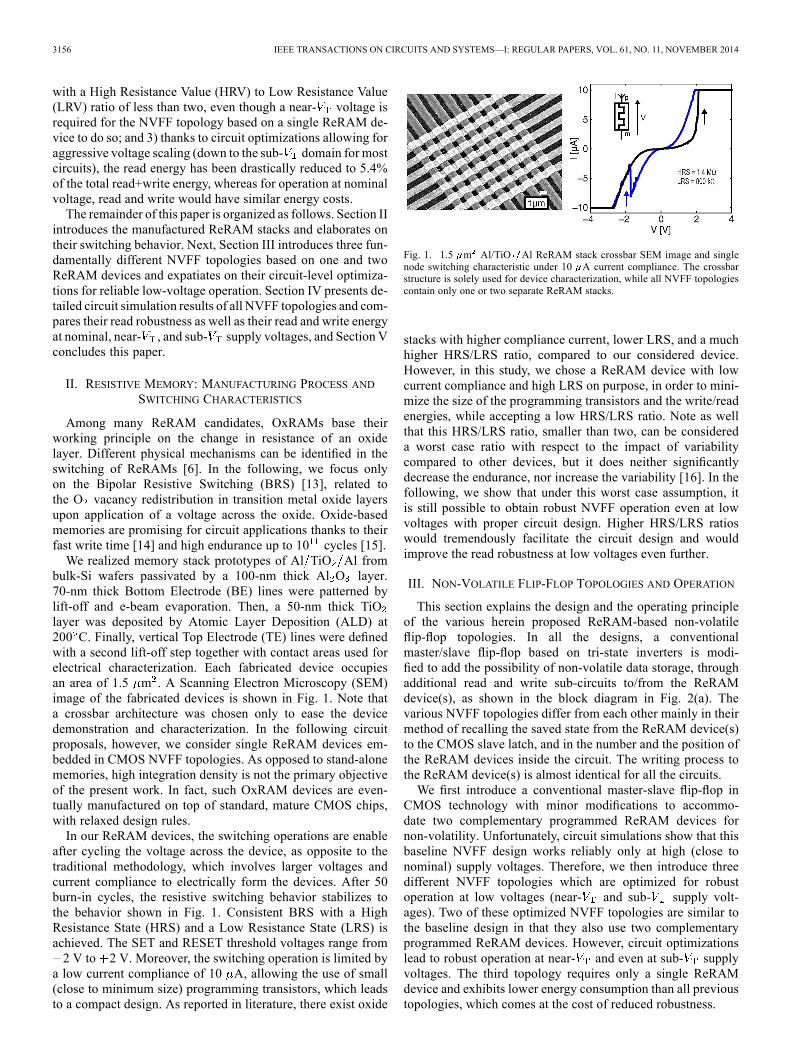
Among many ReRAM candidates, OxRAMs base theirworking principle on the change in resistance of an oxidelayer. Different physical mechanisms can be identified in theswitching of ReRAMs [6]. In the following, we focus onlyon the Bipolar Resistive Switching (BRS) [13], related tothe O vacancy redistribution in transition metal oxide layersupon application of a voltage across the oxide. Oxide-basedmemories are promising for circuit applications thanks to theirfast write time [14] and high endurance up to 10 cycles [15].We realized memory stack prototypes of Al TiO Al from
bulk-Si wafers passivated by a 100-nm thick Al O layer.70-nm thick Bottom Electrode (BE) lines were patterned bylift-off and e-beam evaporation. Then, a 50-nm thick TiOlayer was deposited by Atomic Layer Deposition (ALD) at200 C. Finally, vertical Top Electrode (TE) lines were definedwith a second lift-off step together with contact areas used forelectrical characterization. Each fabricated device occupiesan area of 1.5 m . A Scanning Electron Microscopy (SEM)image of the fabricated devices is shown in Fig. 1. Note thata crossbar architecture was chosen only to ease the devicedemonstration and characterization. In the following circuitproposals, however, we consider single ReRAM devices em-bedded in CMOS NVFF topologies. As opposed to stand-alonememories, high integration density is not the primary objectiveof the present work. In fact, such OxRAM devices are even-tually manufactured on top of standard, mature CMOS chips,with relaxed design rules.In our ReRAM devices, the switching operations are enable
after cycling the voltage across the device, as opposite to thetraditional methodology, which involves larger voltages andcurrent compliance to electrically form the devices. After 50burn-in cycles, the resistive switching behavior stabilizes tothe behavior shown in Fig. 1. Consistent BRS with a HighResistance State (HRS) and a Low Resistance State (LRS) isachieved. The SET and RESET threshold voltages range from2 V to 2 V. Moreover, the switching operation is limited by
a low current compliance of 10 A, allowing the use of small(close to minimum size) programming transistors, which leadsto a compact design. As reported in literature, there exist oxide
Fig. 1. 1.5 m Al/TiO Al ReRAM stack crossbar SEM image and singlenode switching characteristic under 10 A current compliance. The crossbarstructure is solely used for device characterization, while all NVFF topologiescontain only one or two separate ReRAM stacks.
stacks with higher compliance current, lower LRS, and a muchhigher HRS/LRS ratio, compared to our considered device.However, in this study, we chose a ReRAM device with lowcurrent compliance and high LRS on purpose, in order to mini-mize the size of the programming transistors and the write/readenergies, while accepting a low HRS/LRS ratio. Note as wellthat this HRS/LRS ratio, smaller than two, can be considereda worst case ratio with respect to the impact of variabilitycompared to other devices, but it does neither significantlydecrease the endurance, nor increase the variability [16]. In thefollowing, we show that under this worst case assumption, itis still possible to obtain robust NVFF operation even at lowvoltages with proper circuit design. Higher HRS/LRS ratioswould tremendously facilitate the circuit design and wouldimprove the read robustness at low voltages even further.
III. NON-VOLATILE FLIP-FLOP TOPOLOGIES AND OPERATION
This section explains the design and the operating principleof the various herein proposed ReRAM-based non-volatileflip-flop topologies. In all the designs, a conventionalmaster/slave flip-flop based on tri-state inverters is modi-fied to add the possibility of non-volatile data storage, throughadditional read and write sub-circuits to/from the ReRAMdevice(s), as shown in the block diagram in Fig. 2(a). Thevarious NVFF topologies differ from each other mainly in theirmethod of recalling the saved state from the ReRAM device(s)to the CMOS slave latch, and in the number and the position ofthe ReRAM devices inside the circuit. The writing process tothe ReRAM device(s) is almost identical for all the circuits.We first introduce a conventional master-slave flip-flop in
CMOS technology with minor modifications to accommo-date two complementary programmed ReRAM devices fornon-volatility. Unfortunately, circuit simulations show that thisbaseline NVFF design works reliably only at high (close tonominal) supply voltages. Therefore, we then introduce threedifferent NVFF topologies which are optimized for robustoperation at low voltages (near- and sub- supply volt-ages). Two of these optimized NVFF topologies are similar tothe baseline design in that they also use two complementaryprogrammed ReRAM devices. However, circuit optimizationslead to robust operation at near- and even at sub- supplyvoltages. The third topology requires only a single ReRAMdevice and exhibits lower energy consumption than all previoustopologies, which comes at the cost of reduced robustness.

KAZI et al.: ENERGY/RELIABILITY TRADE-OFFS IN LOW-VOLTAGE RERAM-BASED NON-VOLATILE FLIP-FLOP DESIGN 3157
Fig. 2. (a) Conceptual block diagram of a non-volatile flip-flop; and (b) conventional master-slave flip-flop.
Fig. 3. (a) Baseline non-volatile flip-flop design (NVFF-0); (b) control signals sequence for ReRAM read and write operations for the complementary ReRAM-based NVFF circuits; (c) sub- optimized NVFF structure, based on NVFF-0 topology (NVFF-I); and (d) sub- optimized NVFF structure, inspired from [18](NVFF-II).
A. Baseline Non-Volatile Flip-Flop (NVFF-0)
In order to enhance a conventional CMOS flip-flop struc-ture, such as the one shown in Fig. 2(b), with non-volatile datastorage, two ReRAM devices are inserted in the current sink ofthe cross-coupled inverter pair in the slave latch. The resultingbaseline circuit, referred to as NVFF-0, is shown in Fig. 3(a). Asimilar circuit topology has been used in [17], which, however,used magnetic memory devices. In this baseline NVFF, the twoReRAM devices are always used in a complementary fashion,i.e., one device is programmed to the HRS, while the other oneis programmed to the LRS. Dedicated non-volatile program-ming (or ReRAM write) circuits are highlighted in red color in
Fig. 3(a), while dedicated restore on wake-up (or ReRAM read)circuits are shown in black color.ReRAM Read Operation: During system wake-up
(power-on), the slave latch would ideally be directly restored,based on the data stored in the ReRAM devices, during ramp-upor connection of the power supply. However, this is impos-sible due to a number of reasons: 1) the clock and thesignal are not controlled yet; 2) there might be uncontrolled,residual charges on the internal nodes and ; and 3) differentpower-gating approaches (mechanical, footer and/or headertransistors, driving the supply to ground level) result in dif-ferent wake-up scenarios. Therefore, the following wake-upsequence is proposed, as shown in Fig. 3(b): 1) turn on the

3158 IEEE TRANSACTIONS ON CIRCUITS AND SYSTEMS—I: REGULAR PAPERS, VOL. 61, NO. 11, NOVEMBER 2014
power supply; 2) at the system level, silence the clock signal tolow; 3) enable the and the control signals;and 4) upon de-assertion of , the slave latch iscorrectly restored based on the value of the ReRAM devices.Using this wake-up sequence, both internal storage nodesand are first pre-charged and equalized using three dedicatedPMOS transistors controlled by . Following thispre-charge phase, the internal nodes and are connectedto ground through the ReRAM devices. The complementaryresistance states of the two ReRAM devices modulate thedischarge currents (the branch with HRS has a lower dischargecurrent w.r.t. the branch with LRS), starting a race condition.As soon as one internal node is discharged to ,the PMOS transistor driven by that node turns on and starts topull up the other internal node. This decides the race, beforethe feedback of the latch restores full logic levels.ReRAM Write Operation: Prior to an active-to-sleep transi-
tion, the data stored in the slave latch needs to be written to thenon-volatile ReRAMdevices. To this end, as shown in Fig. 3(b),the clock is silenced and kept low for the entire duration ofthe ReRAM write operation, thereby forcing the slave latch tobe non-transparent and isolated from the master. As shown inFig. 3(a), during write, the ReRAM devices are completely dis-connected from the slave latch and from the read circuits, so thatthe voltage drop across their terminals can be set by the writedrivers (highlighted in red). The write drivers are controlled bythe internal nodes and . In general, the write pulse widthdepends on the chosen ReRAM technology. Here, a write pulsewidth of 10 ns is used to successfully program the ReRAM de-vices. As previously illustrated in Fig. 1, a voltage of 2 V or2 V is required for successful switching. To be able to use
small programming transistors (with a non-negligible voltagedrop across their channel) and limit the programming current,the write drivers are supplied with a voltage as high as 2.4 V.This voltage is only slightly above the nominal supply voltagerange of the core transistors in the considered 0.18 m CMOStechnology and does neither seriously enhance the risk of oxidebreakdown, nor compromise junction reliability, nor consider-ably accelerate aging.While the ReRAM write operation requires a high voltage,
the ReRAM read operation as well as the normal flip-flop oper-ation can be performed at scaled voltages for better energy effi-ciency. Several architectural alternatives for the distribution ofthe high supply voltage are discussed in [12]. Here, we adopt theapproach of dynamically rising the supply voltage of all NVFFsduring a write operation, as shown in Fig. 3(b).Normal Operation and Endurance: Note that during normal
operation, the presented hybrid CMOS/ReRAM NVFF, andall other NVFF topologies introduced in the following, fullyrely on CMOS transistors, which are known to exhibit highendurance. The part of the NVFF circuits containing ReRAMdevices, whose endurance is not yet comparable with the oneof CMOS transistors, do not switch very frequently (onlyduring active-to-sleep state transitions), which guarantees highoverall system endurance. Finally, note that the setup and holdtimes during normal operation of all herein proposed NVFFtopologies are solely determined by the master latch and arenot affected by the insertion of the ReRAM devices in theslave latch. The data call window of the presented NVFFs istherefore equal to the one of the conventional CMOS flip-flopshown in Fig. 2(b).
B. NVFF Topologies for Robust Sub- and Near-Operation (NVFF-I and NVFF-II)
For the baseline NVFF circuit (NVFF-0) shown in Fig. 3(a),a correct read operation depends on the modulation of thedischarge currents (discharging nodes and ) by the com-plementary ReRAM devices. However, the discharge currentsmight be altered due to the following reasons: 1) differentpull-down networks in the two branches due to the use ofeither a simple or a tri-state inverter; and 2) mismatch betweenthe transistor pairs (in the inverters and in the dedicated readtransistors) and the ReRAMs, caused by local variations.Post-layout circuit simulations show that the read operation ofthe NVFF-0 circuit works reliably at nominal supply voltage,whereas the Pull-Down Network (PDN) mismatch other thanthe complementary resitance values leads to read failures atlow voltages (see Section IV for detailed simulation results).Therefore, in order to enable the straightforward integration ofReRAM-based NVFFs into ultra-low power VLSI SoCs, i.e.,operated in the near- or sub- domain, we introduce inthe following two NVFF topologies which are optimized foroperation at low voltages.The two sub- optimized NVFF-I and NVFF-II structures
are shown in Fig. 3(d) and Fig. 3(c), respectively, with the ded-icated programming (ReRAM write) circuits highlighted in redand the restore (ReRAM read) circuits in black. Both NVFF-Iand NVFF-II use the same control signal sequence, shown inFig. 3(b) during active-to-sleep and sleep-to-active transitionsas the baseline circuit NVFF-0. Similarly to NVFF-0, the twoReRAM devices are used in a complementary way, i.e., one de-vice is programmed to the HRS, while the other one is pro-grammed to the LRS. The main difference between these twoarchitectures is the connection of the read circuit to the slavelatch of the CMOS flip-flop. Inspired by [18], the read circuit ofNVFF-II is connected to the output nodes, and , while, inthe NVFF-I topology, it is connected to the source of the NMOStransistors of the slave latch. Hence, during read operation, thePDN of NVFF-II consists of only the portion shown in black,whereas for NVFF-I, the PDN is composed of the circuit shownin black and the NMOS transistors shown in blue (which arepart of the inverters forming the slave latch).Since it is crucial to modulate the discharge current of the
precharged nodes and exclusively by the value of theReRAM devices to ensure correct read at low voltages, anyother type of mismatch in the PDN needs to be avoided. Tothis end, in case of NVFF-I, two always-on transistors (and ) are inserted into the simple inverter (used in NVFF-0)to mimic the tri-state inverter in the other pull-down branch.The insertion of dummy transistors can be avoided in theNVFF-II topology, because the ReRAMs are connected to theoutput nodes rather than integrated in the PDN of the inverters.Moreover, all transistor pairs in the PDNs of both NVFF-I andNVFF-II are upsized to further improve matching (see Fig. 3(d)and Fig. 3(c) for the exact transistor dimensions).
C. NVFF Topology With Single ReRAM Device (NVFF-III)
All NVFF topologies considered so far require two ReRAMdevices and a non-trivial wake-up sequence. Unfortunately, thetotal write energy increases with the number of ReRAM devicesused in the NVFF topology. Therefore, this section proposes an
KAZI et al.: ENERGY/RELIABILITY TRADE-OFFS IN LOW-VOLTAGE RERAM-BASED NON-VOLATILE FLIP-FLOP DESIGN 3159
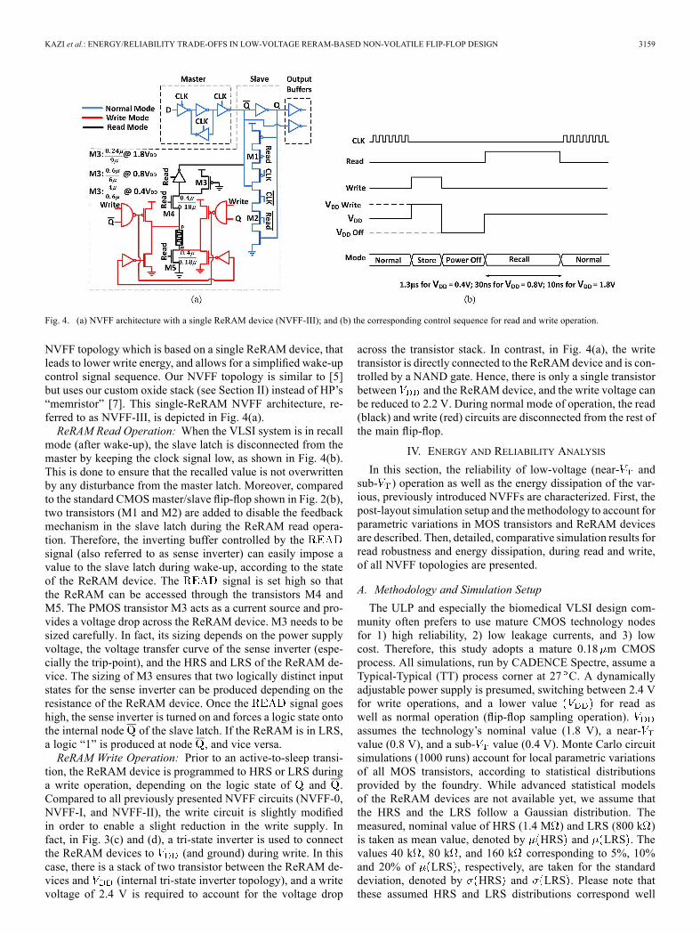
Fig. 4. (a) NVFF architecture with a single ReRAM device (NVFF-III); and (b) the corresponding control sequence for read and write operation.
NVFF topology which is based on a single ReRAM device, thatleads to lower write energy, and allows for a simplified wake-upcontrol signal sequence. Our NVFF topology is similar to [5]but uses our custom oxide stack (see Section II) instead of HP’s“memristor” [7]. This single-ReRAM NVFF architecture, re-ferred to as NVFF-III, is depicted in Fig. 4(a).ReRAM Read Operation: When the VLSI system is in recall
mode (after wake-up), the slave latch is disconnected from themaster by keeping the clock signal low, as shown in Fig. 4(b).This is done to ensure that the recalled value is not overwrittenby any disturbance from the master latch. Moreover, comparedto the standard CMOS master/slave flip-flop shown in Fig. 2(b),two transistors (M1 and M2) are added to disable the feedbackmechanism in the slave latch during the ReRAM read opera-tion. Therefore, the inverting buffer controlled by thesignal (also referred to as sense inverter) can easily impose avalue to the slave latch during wake-up, according to the stateof the ReRAM device. The signal is set high so thatthe ReRAM can be accessed through the transistors M4 andM5. The PMOS transistor M3 acts as a current source and pro-vides a voltage drop across the ReRAM device. M3 needs to besized carefully. In fact, its sizing depends on the power supplyvoltage, the voltage transfer curve of the sense inverter (espe-cially the trip-point), and the HRS and LRS of the ReRAM de-vice. The sizing of M3 ensures that two logically distinct inputstates for the sense inverter can be produced depending on theresistance of the ReRAM device. Once the signal goeshigh, the sense inverter is turned on and forces a logic state ontothe internal node of the slave latch. If the ReRAM is in LRS,a logic “1” is produced at node , and vice versa.ReRAM Write Operation: Prior to an active-to-sleep transi-
tion, the ReRAM device is programmed to HRS or LRS duringa write operation, depending on the logic state of and .Compared to all previously presented NVFF circuits (NVFF-0,NVFF-I, and NVFF-II), the write circuit is slightly modifiedin order to enable a slight reduction in the write supply. Infact, in Fig. 3(c) and (d), a tri-state inverter is used to connectthe ReRAM devices to (and ground) during write. In thiscase, there is a stack of two transistor between the ReRAM de-vices and (internal tri-state inverter topology), and a writevoltage of 2.4 V is required to account for the voltage drop
across the transistor stack. In contrast, in Fig. 4(a), the writetransistor is directly connected to the ReRAMdevice and is con-trolled by a NAND gate. Hence, there is only a single transistorbetween and the ReRAM device, and the write voltage canbe reduced to 2.2 V. During normal mode of operation, the read(black) and write (red) circuits are disconnected from the rest ofthe main flip-flop.
IV. ENERGY AND RELIABILITY ANALYSIS
In this section, the reliability of low-voltage (near- andsub- ) operation as well as the energy dissipation of the var-ious, previously introduced NVFFs are characterized. First, thepost-layout simulation setup and themethodology to account forparametric variations in MOS transistors and ReRAM devicesare described. Then, detailed, comparative simulation results forread robustness and energy dissipation, during read and write,of all NVFF topologies are presented.
A. Methodology and Simulation Setup
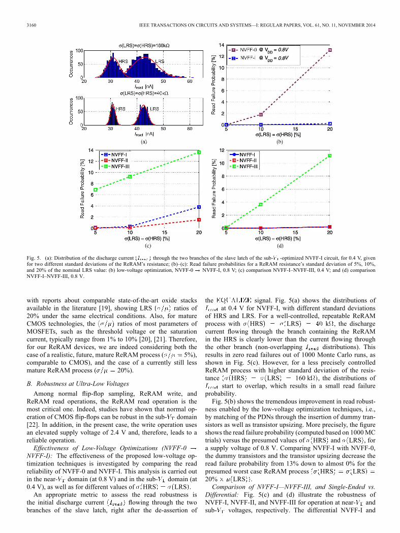
The ULP and especially the biomedical VLSI design com-munity often prefers to use mature CMOS technology nodesfor 1) high reliability, 2) low leakage currents, and 3) lowcost. Therefore, this study adopts a mature 0.18 m CMOSprocess. All simulations, run by CADENCE Spectre, assume aTypical-Typical (TT) process corner at 27 C. A dynamicallyadjustable power supply is presumed, switching between 2.4 Vfor write operations, and a lower value for read aswell as normal operation (flip-flop sampling operation).assumes the technology’s nominal value (1.8 V), a near-value (0.8 V), and a sub- value (0.4 V). Monte Carlo circuitsimulations (1000 runs) account for local parametric variationsof all MOS transistors, according to statistical distributionsprovided by the foundry. While advanced statistical modelsof the ReRAM devices are not available yet, we assume thatthe HRS and the LRS follow a Gaussian distribution. Themeasured, nominal value of HRS (1.4 M ) and LRS (800 k )is taken as mean value, denoted by HRS and LRS . Thevalues 40 k , 80 k , and 160 k corresponding to 5%, 10%and 20% of LRS , respectively, are taken for the standarddeviation, denoted by HRS and LRS . Please note thatthese assumed HRS and LRS distributions correspond well
3160 IEEE TRANSACTIONS ON CIRCUITS AND SYSTEMS—I: REGULAR PAPERS, VOL. 61, NO. 11, NOVEMBER 2014
Fig. 5. (a): Distribution of the discharge current through the two branches of the slave latch of the sub- -optimized NVFF-I circuit, for 0.4 V, givenfor two different standard deviations of the ReRAM’s resistance; (b)–(c): Read failure probabilities for a ReRAM resistance’s standard deviation of 5%, 10%,and 20% of the nominal LRS value: (b) low-voltage optimization, NVFF-0 NVFF-I, 0.8 V; (c) comparison NVFF-I–NVFF-III, 0.4 V; and (d) comparisonNVFF-I–NVFF-III, 0.8 V.
with reports about comparable state-of-the-art oxide stacksavailable in the literature [19], showing LRS ratios of20% under the same electrical conditions. Also, for matureCMOS technologies, the ratios of most parameters ofMOSFETs, such as the threshold voltage or the saturationcurrent, typically range from 1% to 10% [20], [21]. Therefore,for our ReRAM devices, we are indeed considering both thecase of a realistic, future, mature ReRAM process ( 5%),comparable to CMOS), and the case of a currently still lessmature ReRAM process ( 20%).
B. Robustness at Ultra-Low Voltages
Among normal flip-flop sampling, ReRAM write, andReRAM read operations, the ReRAM read operation is themost critical one. Indeed, studies have shown that normal op-eration of CMOS flip-flops can be robust in the sub- domain[22]. In addition, in the present case, the write operation usesan elevated supply voltage of 2.4 V and, therefore, leads to areliable operation.Effectiveness of Low-Voltage Optimizations (NVFF-0
NVFF-I): The effectiveness of the proposed low-voltage op-timization techniques is investigated by comparing the readreliability of NVFF-0 and NVFF-I. This analysis is carried outin the near- domain (at 0.8 V) and in the sub- domain (at0.4 V), as well as for different values of HRS LRS .An appropriate metric to assess the read robustness is
the initial discharge current flowing through the twobranches of the slave latch, right after the de-assertion of
the signal. Fig. 5(a) shows the distributions ofat 0.4 V for NVFF-I, with different standard deviations
of HRS and LRS. For a well-controlled, repeatable ReRAMprocess with HRS LRS k , the dischargecurrent flowing through the branch containing the ReRAMin the HRS is clearly lower than the current flowing throughthe other branch (non-overlapping distributions). Thisresults in zero read failures out of 1000 Monte Carlo runs, asshown in Fig. 5(c). However, for a less precisely controlledReRAM process with higher standard deviation of the resis-tance HRS LRS 160 k , the distributions of
start to overlap, which results in a small read failureprobability.Fig. 5(b) shows the tremendous improvement in read robust-
ness enabled by the low-voltage optimization techniques, i.e.,by matching of the PDNs through the insertion of dummy tran-sistors as well as transistor upsizing. More precisely, the figureshows the read failure probability (computed based on 1000MCtrials) versus the presumed values of HRS and LRS , fora supply voltage of 0.8 V. Comparing NVFF-I with NVFF-0,the dummy transistors and the transistor upsizing decrease theread failure probability from 13% down to almost 0% for thepresumed worst case ReRAM process HRS LRS20% LRS .Comparison of NVFF-I—NVFF-III, and Single-Ended vs.
Differential: Fig. 5(c) and (d) illustrate the robustness ofNVFF-I, NVFF-II, and NVFF-III for operation at near- andsub- voltages, respectively. The differential NVFF-I and
KAZI et al.: ENERGY/RELIABILITY TRADE-OFFS IN LOW-VOLTAGE RERAM-BASED NON-VOLATILE FLIP-FLOP DESIGN 3161
Fig. 6. (a) Read energy; and (b) write energy comparisons for different main supply voltages . Note that the voltage is always risen to 2.4 V for ReRAMwrite.
NVFF-II topologies exhibit a much lower read failure proba-bility than the single-ended NVFF-III topology. In NVFF-III,accuracy is also needed for the current source (transistor M3),to create an appropriate drop across the ReRAM device. If thevalue of the generated current deviates from its nominal value,the sense inverter might switch erroneously, giving rise to readfailures. Conversely, in NVFF-I and NVFF-II only relativeaccuracy is needed. This is why they are more robust thanNVFF-III, both at near- and sub- supply voltages. For anear- supply voltage, NVFF-I and NVFF-II exhibit no readfailures for HRS LRS 10% LRS , whereasNVFF-III exhibits a read failure rate of almost 4% under thesame conditions. Briefly, a differential structure using two com-plementary programmed ReRAM devices is more robust thana single-ended structure employing a single ReRAM device.Finally, NVFF-II reads more reliably in the sub- domain
(at 0.4 V) than NVFF-I, since the former has fewer transistorsand therefore less sources of mismatch in the PDN. In addition,NVFF-II has a slightly smaller area cost than NVFF-I since ituses two transistors less. In conclusion, the differential NVFF-IIis selected as the best-practice circuit for robust operation atultra-low voltages in the sub- domain, whereas the smaller,single-ended NVFF-III circuit is a viable option only down tothe near- domain.
C. Energy Dissipation
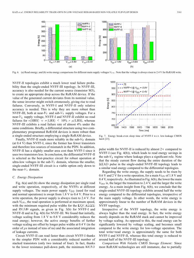
Fig. 6(a) and (b) show the energy dissipation per single readand write operation, respectively, of the NVFFs at differentsupply voltages. The main power supply (used for readand normal operations) is swept from 1.8 V to 0.4 V. Prior to awrite operation, the power supply is always risen to 2.4 V. Foreach , the read operation is performed at maximum speed,with the minimum required pulse widths for theand signals, as given in Fig. 3(b) for NVFF-I andNVFF-II and in Fig. 4(b) for NVFF-III. We found that initially,voltage scaling from 1.8 V to 0.8 V considerably reduces theread energy; however, the active energy benefits of furthervoltage scaling are offset by longer pulse widths at 0.4 V (in theorder of s instead of tens of ns) and the associated integrationof leakage currents.Circuit NVFF-II can read faster than circuit NVFF-I thanks
to the simpler PDN with a considerably reduced number ofstacked transistors (only two instead of four). In fact, thanksto the lower resistance pull-down path, the minimum
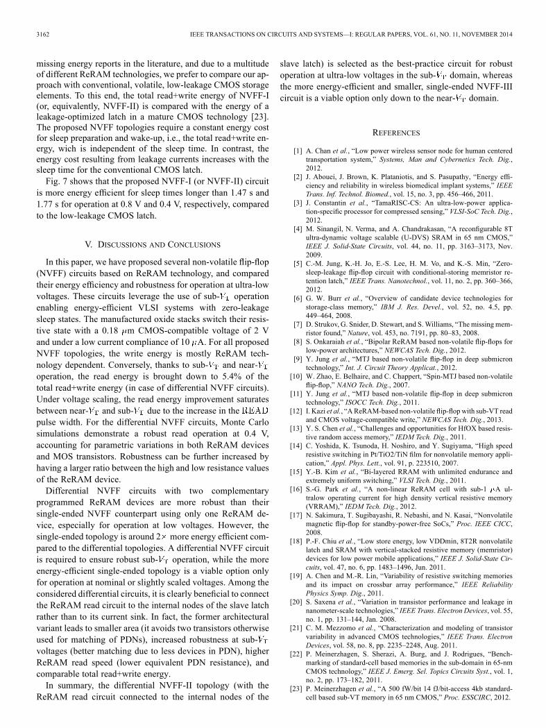
Fig. 7. Energy break-even sleep time of NVFF-I w.r.t. low-leakage CMOSlatch [23].
pulse width for NVFF-II is reduced by almost 2 compared toNVFF-I (see Fig. 4(b)), which leads to read energy savings inthe sub- regime where leakage plays a significant role. Notethat the steady current flow during the entire duration of the
pulse in the single-ended NVFF-III topology leads toa similar read energy compared to the differential topologies.Regarding the write energy, the supply needs to be risen by
0.6 V and 2 V for a write operation, for a main of 1.8 V and0.4 V, respectively. As illustrated in Fig. 6(b), the lower themain
is, the larger the transition to 2.4 V, and the larger the writeenergy. As a main insight from Fig. 6(b), we conclude that thesingle-ended NVFF-III topology exhibits around half the writeenergy compared to the differential topologies, irrespective ofthe main supply voltage. In other words, the write energy isapproximately linear to the number of ReRAM devices in theNVFF topology.Irrespective of the NVFF topology, the write energy is
always higher than the read energy. In fact, the write energymostly depends on the ReRAM stack and cannot be improvedby voltage scaling. As opposed to this, the read energy can besignificantly lowered by voltage scaling, and becomes smallcompared to the write energy for low-voltage operation. Thetotal write+read energy is approximately the same for bothNVFF-I and NVFF-II, whereas this total energy is reduced toaround half of the NVFF-III topology.Comparison With Volatile CMOS Storage Element: Since
most ReRAM technologies are still immature, due to partially
3162 IEEE TRANSACTIONS ON CIRCUITS AND SYSTEMS—I: REGULAR PAPERS, VOL. 61, NO. 11, NOVEMBER 2014
missing energy reports in the literature, and due to a multitudeof different ReRAM technologies, we prefer to compare our ap-proach with conventional, volatile, low-leakage CMOS storageelements. To this end, the total read+write energy of NVFF-I(or, equivalently, NVFF-II) is compared with the energy of aleakage-optimized latch in a mature CMOS technology [23].The proposed NVFF topologies require a constant energy costfor sleep preparation and wake-up, i.e., the total read+write en-ergy, wich is independent of the sleep time. In contrast, theenergy cost resulting from leakage currents increases with thesleep time for the conventional CMOS latch.Fig. 7 shows that the proposed NVFF-I (or NVFF-II) circuit
is more energy efficient for sleep times longer than 1.47 s and1.77 s for operation at 0.8 V and 0.4 V, respectively, comparedto the low-leakage CMOS latch.
V. DISCUSSIONS AND CONCLUSIONS
In this paper, we have proposed several non-volatile flip-flop(NVFF) circuits based on ReRAM technology, and comparedtheir energy efficiency and robustness for operation at ultra-lowvoltages. These circuits leverage the use of sub- operationenabling energy-efficient VLSI systems with zero-leakagesleep states. The manufactured oxide stacks switch their resis-tive state with a 0.18 m CMOS-compatible voltage of 2 Vand under a low current compliance of 10 A. For all proposedNVFF topologies, the write energy is mostly ReRAM tech-nology dependent. Conversely, thanks to sub- and near-operation, the read energy is brought down to 5.4% of thetotal read+write energy (in case of differential NVFF circuits).Under voltage scaling, the read energy improvement saturatesbetween near- and sub- due to the increase in thepulse width. For the differential NVFF circuits, Monte Carlosimulations demonstrate a robust read operation at 0.4 V,accounting for parametric variations in both ReRAM devicesand MOS transistors. Robustness can be further increased byhaving a larger ratio between the high and low resistance valuesof the ReRAM device.Differential NVFF circuits with two complementary
programmed ReRAM devices are more robust than theirsingle-ended NVFF counterpart using only one ReRAM de-vice, especially for operation at low voltages. However, thesingle-ended topology is around 2 more energy efficient com-pared to the differential topologies. A differential NVFF circuitis required to ensure robust sub- operation, while the moreenergy-efficient single-ended topology is a viable option onlyfor operation at nominal or slightly scaled voltages. Among theconsidered differential circuits, it is clearly beneficial to connectthe ReRAM read circuit to the internal nodes of the slave latchrather than to its current sink. In fact, the former architecturalvariant leads to smaller area (it avoids two transistors otherwiseused for matching of PDNs), increased robustness at sub-voltages (better matching due to less devices in PDN), higherReRAM read speed (lower equivalent PDN resistance), andcomparable total read+write energy.In summary, the differential NVFF-II topology (with the
ReRAM read circuit connected to the internal nodes of the
slave latch) is selected as the best-practice circuit for robustoperation at ultra-low voltages in the sub- domain, whereasthe more energy-efficient and smaller, single-ended NVFF-IIIcircuit is a viable option only down to the near- domain.
REFERENCES
[1] A. Chan et al., “Low power wireless sensor node for human centeredtransportation system,” Systems, Man and Cybernetics Tech. Dig.,2012.
[2] J. Abouei, J. Brown, K. Plataniotis, and S. Pasupathy, “Energy effi-ciency and reliability in wireless biomedical implant systems,” IEEETrans. Inf. Technol. Biomed., vol. 15, no. 3, pp. 456–466, 2011.
[3] J. Constantin et al., “TamaRISC-CS: An ultra-low-power applica-tion-specific processor for compressed sensing,” VLSI-SoC Tech. Dig.,2012.
[4] M. Sinangil, N. Verma, and A. Chandrakasan, “A reconfigurable 8Tultra-dynamic voltage scalable (U-DVS) SRAM in 65 nm CMOS,”IEEE J. Solid-State Circuits, vol. 44, no. 11, pp. 3163–3173, Nov.2009.
[5] C.-M. Jung, K.-H. Jo, E.-S. Lee, H. M. Vo, and K.-S. Min, “Zero-sleep-leakage flip-flop circuit with conditional-storing memristor re-tention latch,” IEEE Trans. Nanotechnol., vol. 11, no. 2, pp. 360–366,2012.
[6] G. W. Burr et al., “Overview of candidate device technologies forstorage-class memory,” IBM J. Res. Devel., vol. 52, no. 4.5, pp.449–464, 2008.
[7] D. Strukov, G. Snider, D. Stewart, and S.Williams, “The missing mem-ristor found,” Nature, vol. 453, no. 7191, pp. 80–83, 2008.
[8] S. Onkaraiah et al., “Bipolar ReRAM based non-volatile flip-flops forlow-power architectures,” NEWCAS Tech. Dig., 2012.
[9] Y. Jung et al., “MTJ based non-volatile flip-flop in deep submicrontechnology,” Int. J. Circuit Theory Applicat., 2012.
[10] W. Zhao, E. Belhaire, and C. Chappert, “Spin-MTJ based non-volatileflip-flop,” NANO Tech. Dig., 2007.
[11] Y. Jung et al., “MTJ based non-volatile flip-flop in deep submicrontechnology,” ISOCC Tech. Dig., 2011.
[12] I. Kazi et al., “AReRAM-based non-volatile flip-flop with sub-VT readand CMOS voltage-compatible write,” NEWCAS Tech. Dig., 2013.
[13] Y. S. Chen et al., “Challenges and opportunities for HfOX based resis-tive random access memory,” IEDM Tech. Dig., 2011.
[14] C. Yoshida, K. Tsunoda, H. Noshiro, and Y. Sugiyama, “High speedresistive switching in Pt/TiO2/TiN film for nonvolatile memory appli-cation,” Appl. Phys. Lett., vol. 91, p. 223510, 2007.
[15] Y.-B. Kim et al., “Bi-layered RRAM with unlimited endurance andextremely uniform switching,” VLSI Tech. Dig., 2011.
[16] S.-G. Park et al., “A non-linear ReRAM cell with sub-1 A ul-tralow operating current for high density vertical resistive memory(VRRAM),” IEDM Tech. Dig., 2012.
[17] N. Sakimura, T. Sugibayashi, R. Nebashi, and N. Kasai, “Nonvolatilemagnetic flip-flop for standby-power-free SoCs,” Proc. IEEE CICC,2008.
[18] P.-F. Chiu et al., “Low store energy, low VDDmin, 8T2R nonvolatilelatch and SRAM with vertical-stacked resistive memory (memristor)devices for low power mobile applications,” IEEE J. Solid-State Cir-cuits, vol. 47, no. 6, pp. 1483–1496, Jun. 2011.
[19] A. Chen and M.-R. Lin, “Variability of resistive switching memoriesand its impact on crossbar array performance,” IEEE ReliabilityPhysics Symp. Dig., 2011.
[20] S. Saxena et al., “Variation in transistor performance and leakage innanometer-scale technologies,” IEEE Trans. Electron Devices, vol. 55,no. 1, pp. 131–144, Jan. 2008.
[21] C. M. Mezzomo et al., “Characterization and modeling of transistorvariability in advanced CMOS technologies,” IEEE Trans. ElectronDevices, vol. 58, no. 8, pp. 2235–2248, Aug. 2011.
[22] P. Meinerzhagen, S. Sherazi, A. Burg, and J. Rodrigues, “Bench-marking of standard-cell based memories in the sub-domain in 65-nmCMOS technology,” IEEE J. Emerg. Sel. Topics Circuits Syst., vol. 1,no. 2, pp. 173–182, 2011.
[23] P. Meinerzhagen et al., “A 500 fW/bit 14 fJ/bit-access 4kb standard-cell based sub-VT memory in 65 nm CMOS,” Proc. ESSCIRC, 2012.

KAZI et al.: ENERGY/RELIABILITY TRADE-OFFS IN LOW-VOLTAGE RERAM-BASED NON-VOLATILE FLIP-FLOP DESIGN 3163
Ibrahim Kazi was born in Pakistan in 1987. Hereceived the B.S. degree in electronics from GhulamIshaq Khan Institute of Engineering Sciences andTechnology, Pakistan, and the M.S. degree in systemon chip design from KTH, Stockholm, Sweden.His M.S. thesis was Low Power Current ModeSigma-Delta ADC using a Ring Oscillator BasedQuantizer. Currently, he is a doctoral student atMICAS, working towards the Ph.D. degree inflexible mixed digital-RF modulators.
Pascal Meinerzhagen (S’10–M’14) received theM.Sc. and B.Sc. degrees, both in electrical engi-neering, from EPFL, Lausanne, Switzerland, in 2008and 2006, respectively. He also received the M.Sc.degree in micro- and nanotechnologies for integratedsystems jointly from Grenoble INP, Politecnico diTorino, and EPFL in 2008. He received the Ph.D.degree in electrical engineering from EPFL inFebruary 2014.He is currently a senior research scientist at Intel
Labs, Intel Corporation, Hillsboro, OR, USA. In2014, he was a post-doctoral fellow and a lecturer at the Bar-Ilan University,Ramat-Gan, Israel, where he established the Advanced Digital VLSI Designcourse. His current research interests are broad, ranging from conventional toemerging memories, to ultra-low power VLSI (biomedical), to error-resilientsystems (wireless communications), to power delivery and power managementtechniques. He has authored/co-authored one invited book chapter, 24 journalarticles and international conference papers (two under review), and threepatent applications.Dr. Meinerzhagen is a reviewer for 15 international journals and conferences,
including IEEE TCAS-I, IEEE TCAS-II, the ElsevierMicroelectronics Journal,and IEEE ISCAS. He has received an Intel Ph.D. fellowship and two best papernominations.
Pierre-Emmanuel Gaillardon (S’10–M’11) re-ceived the Electrical Engineer degree from CPE,Lyon, France, in 2008, the M.Sc. degree from INSA,Lyon, France, in 2008, and the Ph.D. degree inelectrical engineering from the University of Lyon,France, in 2011.He works for EPFL, Lausanne, Switzerland, as
a research associate at the Laboratory of IntegratedSystems (LSI). Previously, he was a research assis-tant at CEA-LETI, Grenoble, France. Involved in theNanosys project, his research activities and interests
are currently focused on emerging nanoscale devices for digital circuits andsystems.Dr. Gaillardon was a recipient of the C-Innov 2011 Best Thesis Award and
the Nanoarch 2012 Best Paper Award. He has served as a TPC member forthe Nanoarch’12–’14, CMOSETR’13–’14, and ISVLSI’14 conferences and isa reviewer for several journals (AIP APL, IEEE TNANO, IEEE TVLSI, ACMJETC), conferences (ICECS, ISCAS), and funding agencies (ANR, Chairs ofExcellence program of Nanosciences Foundation).
Davide Sacchetto (S’12–M’13) received the B.S.degree in physics engineering from Politecnicodi Torino, Italy, in 2007. In 2008 he received thejoint M.S. degree in micro and nano technologiesfor integrated systems from École PolytechniqueFédérale de Lausanne (EPFL), the Institut NationalPolytechnique de Grenoble (INPG), and the Politec-nico di Torino (POLITO). He received the Ph.D.degree in microsystems and microelectronics inSeptember 2013 from EPFL.His research interests focus on novel devices, in-
vestigating issues ranging from solid-state microfabrication to circuit imple-mentation. He is interested in the post-processing fabrication of CMOS tech-nology that can enable integration of CMOS with the additional functionality
that emerging technology can bring. For instance, resistive RAM devices inte-grated with CMOS can bring performance benefits to diverse CMOS applica-tions, such as FPGAs, artificial neural networks, and standalone memories.
Yusuf Leblebici (S’88–M’90–SM’98–F’10) re-ceived the B.Sc. and M.Sc. degrees in electricalengineering from Istanbul Technical University,Istanbul, Turkey, in 1984 and 1986, respectively,and the Ph.D. degree in electrical and computerengineering from the University of Illinois at Ur-bana-Champaign (UIUC), IL, USA, in 1990.Between 1991 and 2001, he worked as a faculty
member at UIUC, at Istanbul Technical University,and at Worcester Polytechnic Institute (WPI). In2000–2001, he also served as the Microelectronics
Program Coordinator at Sabanci University, Turkey. Since 2002, he has beena Chair Professor at the Swiss Federal Institute of Technology in Lausanne(EPFL), and Director of the Microelectronic Systems Laboratory. His researchinterests include design of high-speed CMOS digital and mixed-signal inte-grated circuits, computer-aided design of VLSI systems, intelligent sensorinterfaces, modeling and simulation of semiconductor devices, and VLSIreliability analysis. He is the coauthor of six textbooks, namely, Hot-CarrierReliability of MOS VLSI Circuits (Kluwer Academic, 1993), CMOS DigitalIntegrated Circuits: Analysis and Design (McGraw Hill, 1st ed., 1996, 2nded., 1998, 3rd ed., 2002), CMOS Multichannel Single-Chip Receivers forMulti-Gigabit Optical Data Communications (Springer, 2007), Fundamentalsof High Frequency CMOS Analog Integrated Circuits (Cambridge UniversityPress, 2009), Extreme Low-Power Mixed Signal IC Design (Springer, 2010)and Reliability of Nanoscale Circuits and Systems (Springer, 2011), as well asmore than 250 articles published in various journals and conferences.Dr. Leblebici has served as an Associate Editor of IEEE TRANSACTIONS ON
CIRCUITS AND SYSTEMS II, and IEEE TRANSACTIONS ON VERY LARGE SCALEINTEGRATED (VLSI) SYSTEMS. He has also served as the general co-chair ofthe 2006 European Solid-State Circuits Conference and the 2006 EuropeanSolid State Device Research Conference (ESSCIRC/ESSDERC). He waselected as a Distinguished Lecturer of the IEEE Circuits and Systems Societyfor 2010–2011.
Andreas Burg (S’97–M’05) was born in Munich,Germany, in 1975. He received the Dipl.-Ing. degreefrom the Swiss Federal Institute of Technology(ETH) Zurich, Zurich, Switzerland, in 2000. He thenjoined the Integrated Systems Laboratory of ETHZurich, from which he graduated with the Dr. sc.techn. degree in 2006.In 1998, he worked at Siemens Semiconductors,
San Jose, CA, USA. During his doctoral studies, heworked at Bell Labs Wireless Research for one year.From 2006 to 2007, he held positions as postdoc-
toral researcher at the Integrated Systems Laboratory and at the Communica-tion Theory Group of the ETH Zurich. In 2007, he co-founded Celestrius, anETH-spinoff in the field of MIMO wireless communication, where he was re-sponsible for the ASIC development as Director for VLSI. In January 2009, hejoined ETH Zurich as SNF Assistant Professor and as head of the Signal Pro-cessing Circuits and Systems group at the Integrated Systems Laboratory. SinceJanuary 2011, he has been a tenure-track Assistant Professor at the École Poly-technique Fédérale de Lausanne (EPFL) where he is leading the Telecommu-nications Circuits Laboratory in the School of Engineering. In his professionalcareer, he has been involved in the design of more than 35 ASICs. He has pub-lished more than 120 papers in peer-reviewed conferences and journals.In 2000, Dr. Burg received the Willi Studer Award and the ETH Medal for
his diploma and his diploma thesis, respectively. He was also awarded an ETHMedal for his Ph.D. dissertation in 2006. In 2008, he received a 4-years grantfrom the Swiss National Science Foundation (SNF) for an SNF Assistant Pro-fessorship. In 2013, he received a Best Paper Award from the EURASIP Journalon Image and Video Processing. He has served on the TPC of various confer-ences on VLSI, signal processing, and communications and was a TPC chair forVLSI-SoC 2012. He also served as General Chair for D43D 2012 at EPFL. Heserved as Editor for the IEEE TRANSACTIONS ON CIRCUITS AND SYSTEMS PARTI in 2013, as Editor for the MDJI Journal on Low Power Electronics and Ap-plications since 2012, and as Editor for the Elsevier Microelectronics Journalsince 2014.

3164 IEEE TRANSACTIONS ON CIRCUITS AND SYSTEMS—I: REGULAR PAPERS, VOL. 61, NO. 11, NOVEMBER 2014
Giovanni DeMicheli (M’83–SM’89–F’94) receivedthe Nuclear Engineer degree from Politecnico di Mi-lano, Italy, in 1979, and the M.S. and Ph.D. degreesin electrical engineering and computer science fromthe University of California at Berkeley, CA, USA,in 1980 and 1983, respectively.He is Professor and Director of the Institute of
Electrical Engineering and of the Integrated SystemsCentre at EPF Lausanne, Switzerland, and is programleader of the Nano-Tera.ch program. Previously, hewas Professor of Electrical Engineering at Stanford
University, Stanford, CA, USA. His research interests include several aspectsof design technologies for integrated circuits and systems, such as synthesisfor emerging technologies, networks on chips and 3D integration. He is alsointerested in heterogeneous platform design including electrical componentsand biosensors, as well as in data processing of biomedical information. He isauthor of Synthesis and Optimization of Digital Circuits (McGraw-Hill, 1994),and co-author and/or co-editor of eight other books and of over 600 technicalarticles. His citation h-index is 83 according to Google Scholar.
Prof. De Micheli is a Fellow of ACM and a member of the Academia Eu-ropaea. He is a member of the Scientific Advisory Board of IMEC (Leuven,B), CfAED (Dresden, D) and STMicroelectronics. He was the recipient of the2012 IEEE/CAS Mac Van Valkenburg award for contributions to theory, prac-tice and experimentation in design methods and tools, and of the 2003 IEEEEmanuel Piore Award for contributions to computer-aided synthesis of digitalsystems. He also received the Golden Jubilee Medal for outstanding contribu-tions to the IEEE CAS Society in 2000, the D. Pederson Award for the bestpaper in the IEEE TRANSACTIONS ON CAD/ICAS in 1987, and several BestPaper Awards including DAC (1983 and 1993), DATE (2005), and Nanoarch(2010 and 2012). He has served IEEE in several capacities, including Division1 Director (2008–2009), co-founder and President Elect of the IEEE Councilon EDA (2005–2007), President of the IEEE CAS Society (2003), and Ed-itor-in-Chief of the IEEE TRANSACTIONS ON CAD/ICAS (1997–2001). He hasbeen Chair of several conferences, including DATE (2010), pHealth (2006),VLSI SOC (2006), DAC (2000), and ICCD (1989).