implementing irda data communication using …
TRANSCRIPT
ELECTRONICS’ 2004 22-24 September, Sozopol, BULGARIA
IMPLEMENTING IRDA DATA COMMUNICATION USING HARDWARE DESCRIPTION LANGUAGE
Nikolay Ventzizlavov Krantov, Todor Stoyanov Djamyikov, Stefan Yordanov Ovcharov, Dimitar Serafimov Alexiev
Faculty of electronics, Technical University - Sofia, , BG-1756 Sofia, Bulgaria tel.: (+359)29653269,
e-mails: [email protected], [email protected], [email protected], [email protected]
Keywords: Infra Red communication, RC5 code, CPLD, VHDL, Xilinx
Abstract: IrDA devices provide a walk-up, point-to-point method of data transfer that is adaptable to a broad range of computing and communicating devices.
A UART interface is implemented in this design for data rates up to 37.9 Kbps. This boundary has imposed by used photo-link module by ROHM RPM7138. The IrDA specification is intended for use with a serial communications controller such as a conventional UART.
The UART and IrDA design was implemented in VHDL. Xilinx Project Navigator was used for compilation, fitting, and simulation and programming the design in a CPLD device. There were used two kinds of devices from Xilinx XCR3256XL and XC9572 for testing the design. The first one was configured as transmitter and the second one as receiver, using ROHM IR receiver module as input flow and seven-segment LED indicator as output. There was transmitted consequently changing bit pattern ranging from 0 to F.
1. MODULATION SCHEME
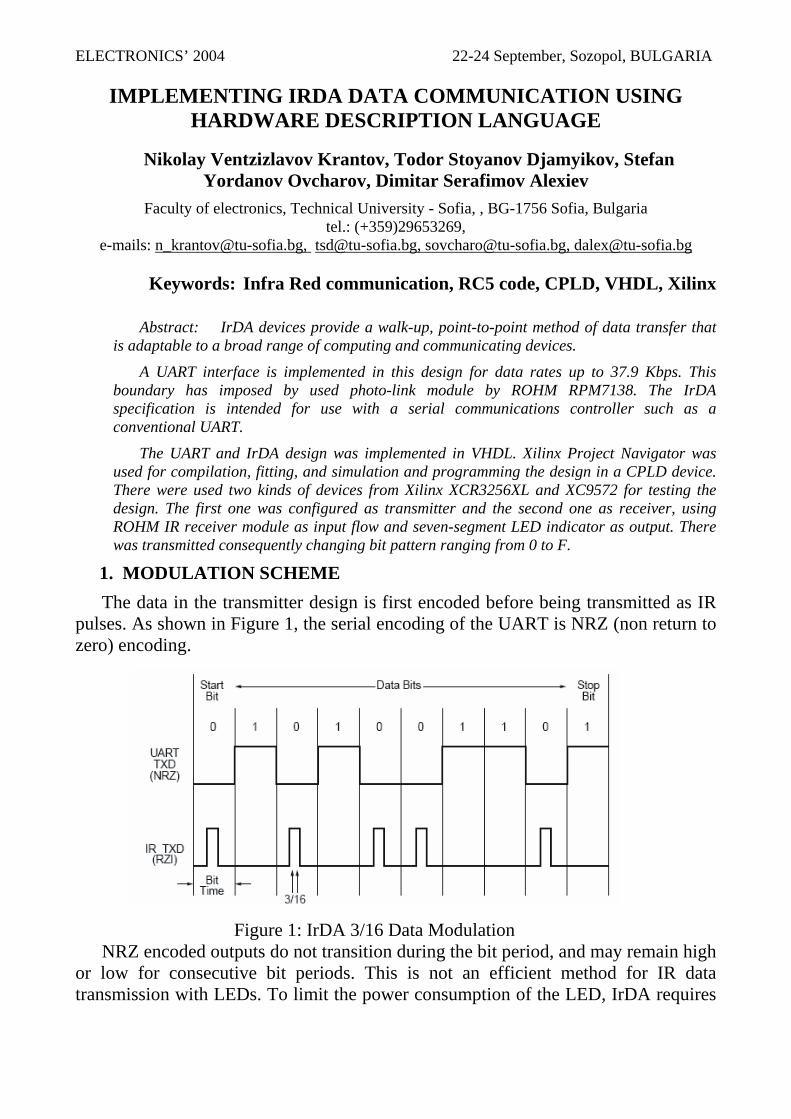
The data in the transmitter design is first encoded before being transmitted as IR pulses. As shown in Figure 1, the serial encoding of the UART is NRZ (non return to zero) encoding.
Figure 1: IrDA 3/16 Data Modulation NRZ encoded outputs do not transition during the bit period, and may remain high
or low for consecutive bit periods. This is not an efficient method for IR data transmission with LEDs. To limit the power consumption of the LED, IrDA requires

ELECTRONICS’ 2004 22-24 September, Sozopol, BULGARIA pulsing the LED in a RZI (return to zero inverted) modulation scheme so that the peak power to average power ratio can be increased. IrDA requires the maximum pulse width to be 3/16th of the bit period. A 16x clock is required, and counting three clock cycles can easily be done to encode the transmitted data. IrDA architecture has used RC5 code for transmitted data because of his high noise immunity.
2. HALF DUPLEX AND LATENCY
The IrDA link cannot send and receive data at the same time. The IrDA link is a half-duplex interface and a time delay must be allowed from when a link stops transmitting until it can receive data again. A time period with duration of 10 ms must be allowed between transmitting and receiving data. The UART interface design is full-duplex, supporting simultaneous read and write operations from the microprocessor or microcontroller interface.
3. IMPLEMENTED ARCHITECTURE
The following figure illustrates the system architecture for implementing a UART serial port interface with an IrDA module in a CoolRunner CPLD. The UART or a discrete device must provide a 16x clock for the IrDA 3/16 modulation scheme.
Figure 2. UART and IrDA Block Diagram
The VHDL code provided in developed design for the UART interface consists of
two independent HDL modules - TRANSMIT and RECEIVE. Data is written to the transmitter and data is read from the receiver through an 8-bit parallel data bus.
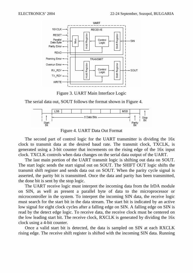
The full the functionality of the UART interface is shown on the figure 3. The data bus interface to the UART module is 8-bits. Even or odd parity can be selected on the serial data out, SOUT.
Data transfer in this design is controlled by the microprocessor or microcontroller like system. The UART design must interface with the parallel bus and necessary control lines. The UART transmit logic consists of interpreting processor write commands, generating the transmit clock, TXCLK, at the desired baud rate, and shifting out data on SOUT. The UART logic must interpret the active low write signal from the processor and read in data from the data bus. The data is read into the transmit hold register. Once the write signal is de-asserted, a flag is asserted to start shifting data out on SOUT.
ELECTRONICS’ 2004 22-24 September, Sozopol, BULGARIA
Figure 3. UART Main Interface Logic
The serial data out, SOUT follows the format shown in Figure 4.
Figure 4. UART Data Out Format
The second part of control logic for the UART transmitter is dividing the 16x
clock to transmit data at the desired baud rate. The transmit clock, TXCLK, is generated using a 3-bit counter that increments on the rising edge of the 16x input clock. TXCLK controls when data changes on the serial data output of the UART.
The last main portion of the UART transmit logic is shifting out data on SOUT. The start logic sends the start signal out on SOUT. The SHIFT OUT logic shifts the transmit shift register and sends data out on SOUT. When the parity cycle signal is asserted, the parity bit is transmitted. Once the data and parity has been transmitted, the done bit is sent by the stop logic.
The UART receive logic must interpret the incoming data from the IrDA module on SIN, as well as present a parallel byte of data to the microprocessor or microcontroller in the system. To interpret the incoming SIN data, the receive logic must search for the start bit in the data stream. The start bit is indicated by an active low signal for eight clock cycles after a falling edge on SIN. A falling edge on SIN is read by the detect edge logic. To receive data, the receive clock must be centered on the low leading start bit. The receive clock, RXCLK is generated by dividing the 16x clock using a 4-bit counter.
Once a valid start bit is detected, the data is sampled on SIN at each RXCLK rising edge. The receive shift register is shifted with the incoming SIN data. Running
ELECTRONICS’ 2004 22-24 September, Sozopol, BULGARIA parity is generated with each incoming data bit. When a stop bit is detected, any error flags are set. There are included parity, overrun, and framing error flags.
A main function of the UART receive logic is interfacing with the processor like system. The CPLD detects a valid edge on the READ signal asserted by the processor. The CPLD then places the received parallel data on the system data bus.
4. IR SYSTEM HARDWARE
The UART and IrDA transmitter and receiver designs were implemented in VHDL as described above.
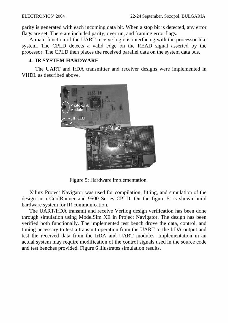
Figure 5: Hardware implementation Xilinx Project Navigator was used for compilation, fitting, and simulation of the
design in a CoolRunner and 9500 Series CPLD. On the figure 5. is shown build hardware system for IR communication.
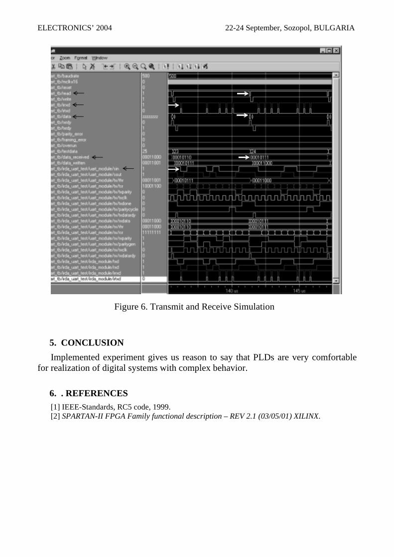
The UART/IrDA transmit and receive Verilog design verification has been done through simulation using ModelSim XE in Project Navigator. The design has been verified both functionally. The implemented test bench drove the data, control, and timing necessary to test a transmit operation from the UART to the IrDA output and test the received data from the IrDA and UART modules. Implementation in an actual system may require modification of the control signals used in the source code and test benches provided. Figure 6 illustrates simulation results.
ELECTRONICS’ 2004 22-24 September, Sozopol, BULGARIA
Figure 6. Transmit and Receive Simulation
5. CONCLUSION
Implemented experiment gives us reason to say that PLDs are very comfortable for realization of digital systems with complex behavior.
6. . REFERENCES [1] IEEE-Standards, RC5 code, 1999. [2] SPARTAN-II FPGA Family functional description – REV 2.1 (03/05/01) XILINX.