i.mx 6ull evk board hardware user's...
TRANSCRIPT
© 2016 NXP B.V.
i.MX 6ULL EVK Board Hardware User's
Guide
1. Introduction
This document is the Hardware User’s Guide for the
i.MX 6ULL Evaluation Kit (EVK) based on the NXP
Semiconductor i.MX 6ULL Applications Processor.
This board is fully supported by NXP Semiconductor.
This Manual includes system setup and debugging, and
provides detailed information on the overall design and
usage of the EVK board from a Hardware Systems
perspective.
1.1. Board overview
The EVK board is a platform designed to showcase many
of the most commonly used features of the i.MX 6ULL
Applications Processor in a small, low cost package.
The i.MX 6ULL EVK board is an entry level
development board, which gives the developer the
option of becoming familiar with the processor before
investing a large amount of resources in more specific
designs.
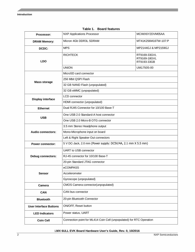
The features of the i.MX 6ULL EVK board are shown
in the following table.
NXP Semiconductors Document Number: IMX6ULLEVKHUG
User's Guide Rev. 0 , 10/2016
Contents
1. Introduction .................................................................... 1 1.1. Board overview .................................................... 1 1.2. i.MX 6ULL EVK contents..................................... 3 1.3. i.MX 6ULL EVK board revision history ................ 3
2. Specifications .................................................................. 4 2.1. i.MX 6ULL processor ........................................... 6 2.2. Boot mode configurations ..................................... 6 2.3. Power tree ............................................................ 8 2.4. DDR3L DRAM memory ..................................... 11 2.5. SD card slots (J301, P1701) ................................. 11 2.6. eMMC ................................................................ 11 2.7. QSPI Nor flash ................................................... 11 2.8. NAND flash ....................................................... 11 2.9. Dual ethernet connector (J1501) .......................... 12 2.10. USB PHY connector (J1102, J1101) .................... 12 2.11. Audio input/output connectors (J1401/P1401/J1402 & J1403) .......................................................................... 12 2.12. USB debug connector (J1901) ............................. 13 2.13. Bluetooth Connector (J1701) ............................... 13 2.14. JTAG connector (J1902) ...................................... 14 2.15. ARDUINO expansion port (J1703-J1706) ............ 15 2.16. User interface switches ....................................... 15 2.17. Sensors ............................................................... 16 2.18. User interface LED indicators ............................. 17 2.19. Optional back-up coin cell holder (BT2101) ........ 17 2.20. LCD daughter card.............................................. 17
3. PCB Information ........................................................... 18 4. EVK Design Files ......................................................... 18 5. Contents of the Evaluation Kit ....................................... 18 6. References .................................................................... 19 7. Revision History ........................................................... 19
Introduction
i.MX 6ULL EVK Board Hardware User's Guide, Rev. 0, 10/2016
2 NXP Semiconductors
Table 1. Board features
Processor: NXP Applications Processor MCIMX6Y2DVM05AA
DRAM Memory: Micron 4Gb DDR3L SDRAM MT41K256M16TW-107:P
DCDC: MPS MP2144GJ & MP2159GJ
LDO
RICHTECK RT9169-33GVL
RT9169-18GVL
RT9193-33GB
UNION UM1750S-00
Mass storage
MicroSD card connector
256 Mbit QSPI Flash
32 GB NAND Flash (unpopulated)
32 GB eMMC (unpopulated)
Display interface
LCD connector
HDMI connector (unpopulated)
Ethernet Dual RJ45 Connector for 10/100 Base-T
USB
One USB 2.0 Standard-A host connector
One USB 2.0 Micro-B OTG connector
Audio connectors:
3.5 mm Stereo Headphone output
Mono-Microphone input on board
Left & Right Speaker Out connectors
Power connector: 5 V DC-Jack, 2.0 mm (Power supply: DC5V/4A, 2.1 mm X 5.5 mm)
Debug connectors:
UART to USB connector
RJ-45 connector for 10/100 Base-T
20-pin Standard JTAG connector
Sensor
eCOMPASS
Accelerometer
Gyroscope (unpopulated)
Camera CMOS Camera connector(unpopulated)
CAN CAN bus connector
Bluetooth 20-pin Bluetooth Connector
User Interface Buttons ON/OFF, Reset button
LED Indicators Power status, UART
Coin Cell Connection point for ML414 Coin Cell (unpopulated) for RTC Operation
Specifications
i.MX 6ULL EVK Board Hardware User's Guide, Rev. 0, 10/2016
NXP Semiconductors 3
Table 1. Board features
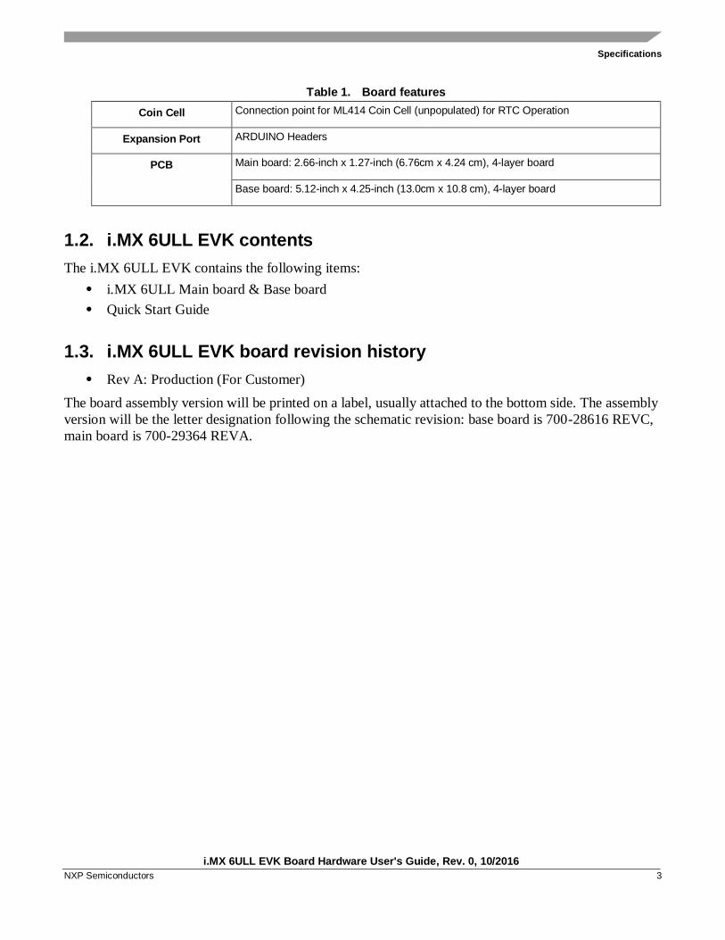
Coin Cell Connection point for ML414 Coin Cell (unpopulated) for RTC Operation
Expansion Port ARDUINO Headers
PCB Main board: 2.66-inch x 1.27-inch (6.76cm x 4.24 cm), 4-layer board
Base board: 5.12-inch x 4.25-inch (13.0cm x 10.8 cm), 4-layer board
1.2. i.MX 6ULL EVK contents
The i.MX 6ULL EVK contains the following items:
• i.MX 6ULL Main board & Base board
• Quick Start Guide
1.3. i.MX 6ULL EVK board revision history
• Rev A: Production (For Customer)
The board assembly version will be printed on a label, usually attached to the bottom side. The assembly
version will be the letter designation following the schematic revision: base board is 700-28616 REVC,
main board is 700-29364 REVA.
Specifications
i.MX 6ULL EVK Board Hardware User's Guide, Rev. 0, 10/2016
4 NXP Semiconductors
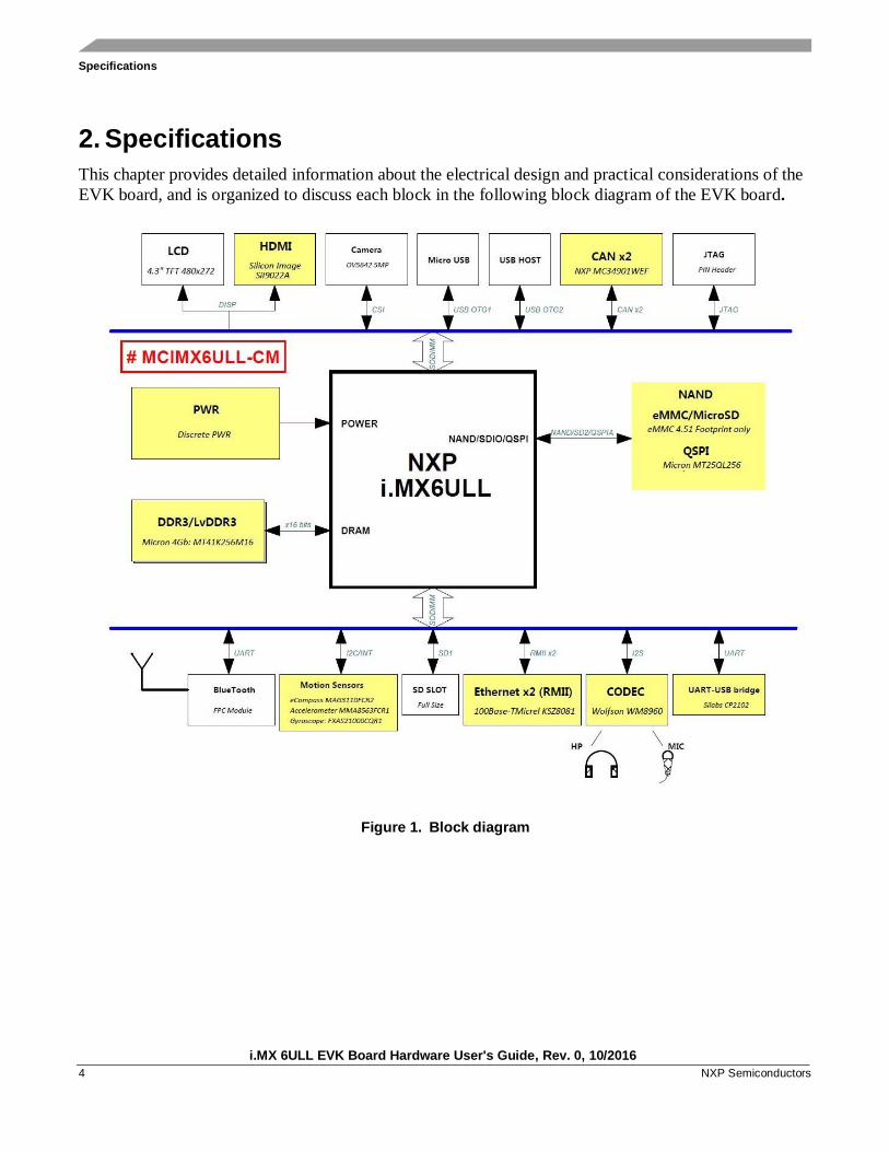
2. Specifications
This chapter provides detailed information about the electrical design and practical considerations of the
EVK board, and is organized to discuss each block in the following block diagram of the EVK board.
Figure 1. Block diagram
Specifications
i.MX 6ULL EVK Board Hardware User's Guide, Rev. 0, 10/2016
NXP Semiconductors 5
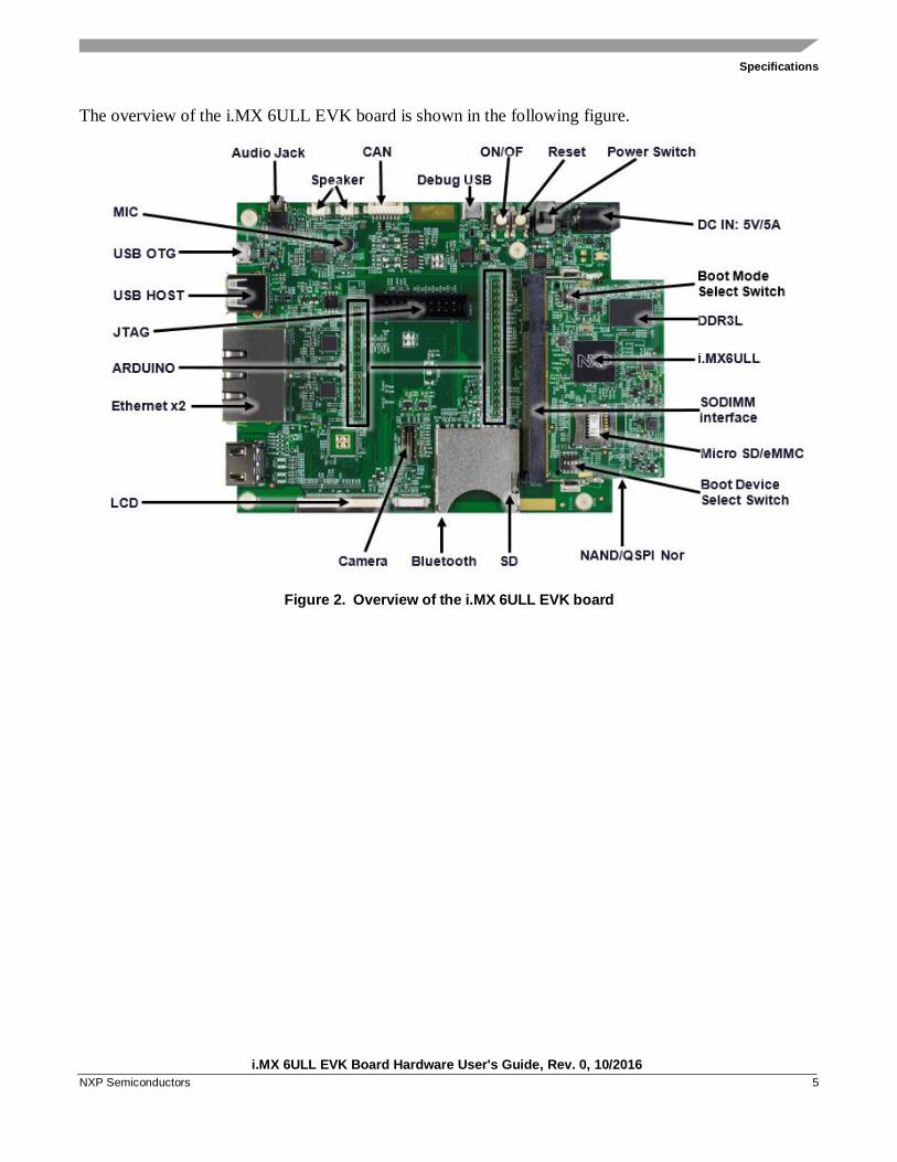
The overview of the i.MX 6ULL EVK board is shown in the following figure.
Figure 2. Overview of the i.MX 6ULL EVK board
Specifications
i.MX 6ULL EVK Board Hardware User's Guide, Rev. 0, 10/2016
6 NXP Semiconductors
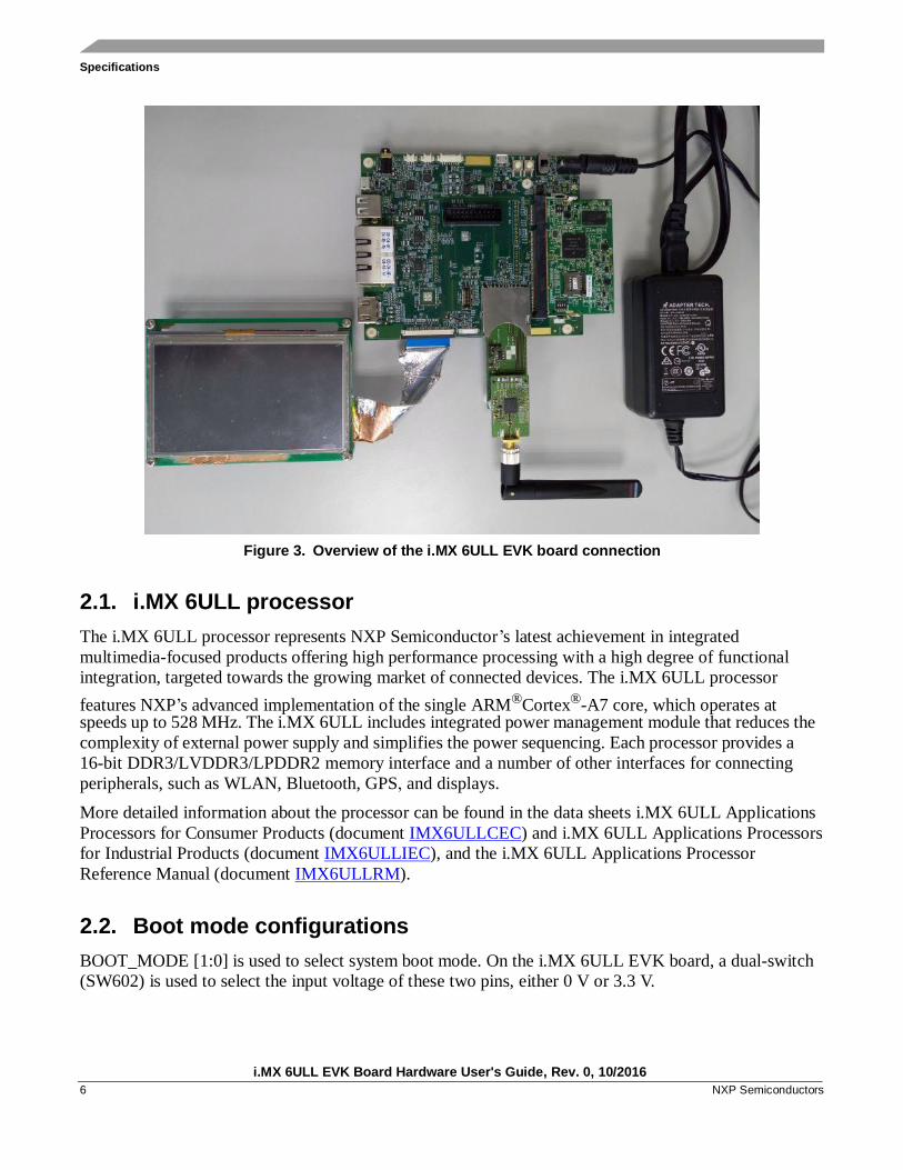
Figure 3. Overview of the i.MX 6ULL EVK board connection
2.1. i.MX 6ULL processor
The i.MX 6ULL processor represents NXP Semiconductor’s latest achievement in integrated
multimedia-focused products offering high performance processing with a high degree of functional
integration, targeted towards the growing market of connected devices. The i.MX 6ULL processor
features NXP’s advanced implementation of the single ARM®Cortex®-A7 core, which operates at speeds up to 528 MHz. The i.MX 6ULL includes integrated power management module that reduces the
complexity of external power supply and simplifies the power sequencing. Each processor provides a
16-bit DDR3/LVDDR3/LPDDR2 memory interface and a number of other interfaces for connecting
peripherals, such as WLAN, Bluetooth, GPS, and displays.
More detailed information about the processor can be found in the data sheets i.MX 6ULL Applications
Processors for Consumer Products (document IMX6ULLCEC) and i.MX 6ULL Applications Processors
for Industrial Products (document IMX6ULLIEC), and the i.MX 6ULL Applications Processor
Reference Manual (document IMX6ULLRM).
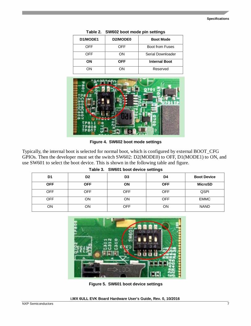
2.2. Boot mode configurations
BOOT_MODE [1:0] is used to select system boot mode. On the i.MX 6ULL EVK board, a dual-switch
(SW602) is used to select the input voltage of these two pins, either 0 V or 3.3 V.
Specifications
i.MX 6ULL EVK Board Hardware User's Guide, Rev. 0, 10/2016
NXP Semiconductors 7
Table 2. SW602 boot mode pin settings
D1/MODE1 D2/MODE0 Boot Mode
OFF OFF Boot from Fuses
OFF ON Serial Downloader
ON OFF Internal Boot
ON ON Reserved
Figure 4. SW602 boot mode settings
Typically, the internal boot is selected for normal boot, which is configured by external BOOT_CFG
GPIOs. Then the developer must set the switch SW602: D2(MODE0) to OFF, D1(MODE1) to ON, and
use SW601 to select the boot device. This is shown in the following table and figure.
Table 3. SW601 boot device settings
D1 D2 D3 D4 Boot Device
OFF OFF ON OFF MicroSD
OFF OFF OFF OFF QSPI
OFF ON ON OFF EMMC
ON ON OFF ON NAND
Figure 5. SW601 boot device settings
Specifications
i.MX 6ULL EVK Board Hardware User's Guide, Rev. 0, 10/2016
8 NXP Semiconductors
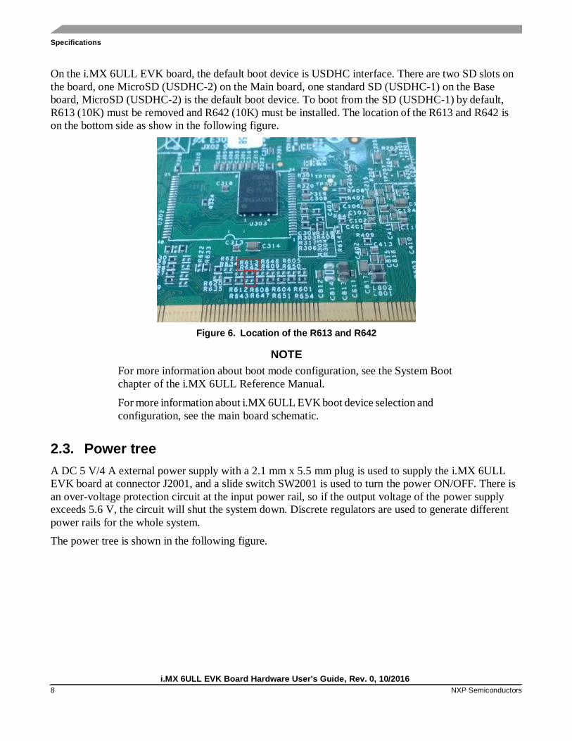
On the i.MX 6ULL EVK board, the default boot device is USDHC interface. There are two SD slots on
the board, one MicroSD (USDHC-2) on the Main board, one standard SD (USDHC-1) on the Base
board, MicroSD (USDHC-2) is the default boot device. To boot from the SD (USDHC-1) by default,
R613 (10K) must be removed and R642 (10K) must be installed. The location of the R613 and R642 is
on the bottom side as show in the following figure.
Figure 6. Location of the R613 and R642
NOTE
For more information about boot mode configuration, see the System Boot
chapter of the i.MX 6ULL Reference Manual.
For more information about i.MX 6ULL EVK boot device selection and
configuration, see the main board schematic.
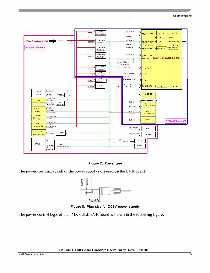
2.3. Power tree
A DC 5 V/4 A external power supply with a 2.1 mm x 5.5 mm plug is used to supply the i.MX 6ULL
EVK board at connector J2001, and a slide switch SW2001 is used to turn the power ON/OFF. There is
an over-voltage protection circuit at the input power rail, so if the output voltage of the power supply
exceeds 5.6 V, the circuit will shut the system down. Discrete regulators are used to generate different
power rails for the whole system.
The power tree is shown in the following figure.
Specifications
i.MX 6ULL EVK Board Hardware User's Guide, Rev. 0, 10/2016
NXP Semiconductors 9
Figure 7. Power tree
The power tree displays all of the power supply rails used on the EVK board.
Figure 8. Plug size for DC5V power supply
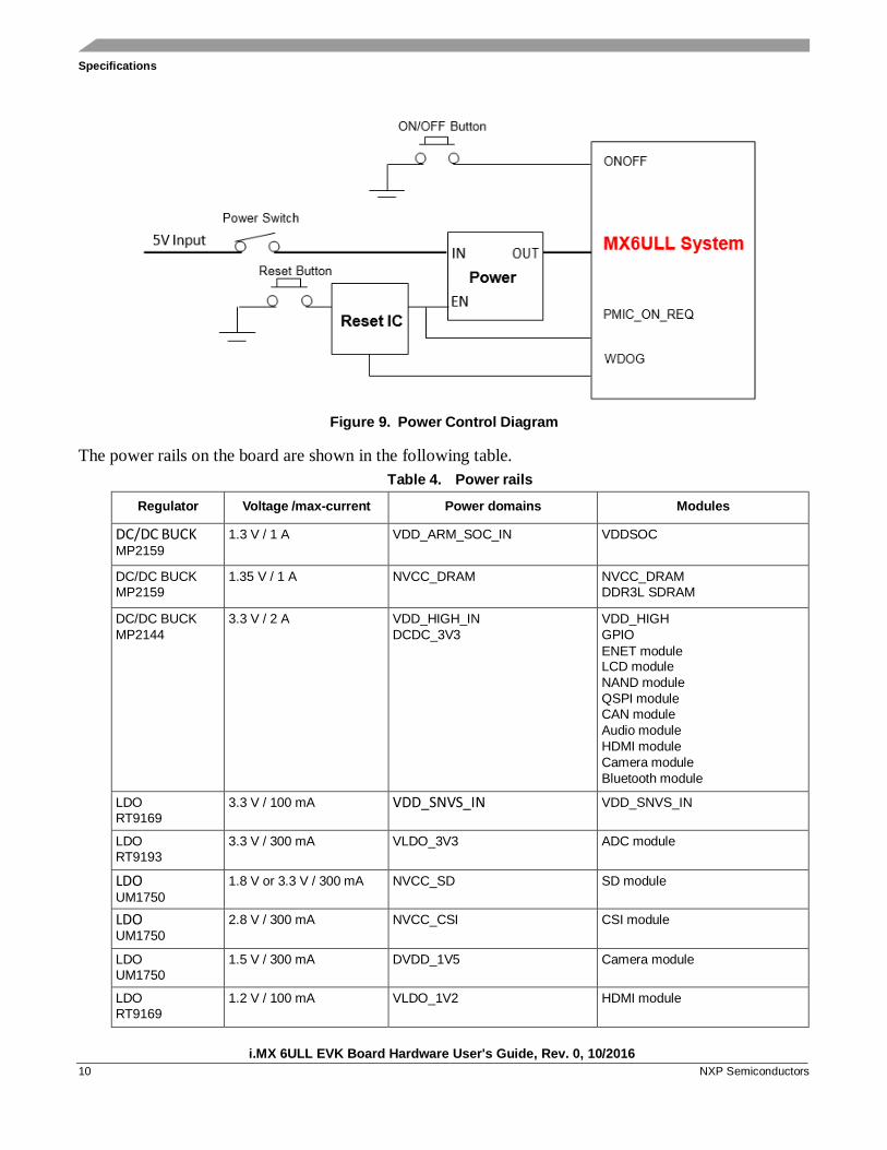
The power control logic of the i.MX 6ULL EVK board is shown in the following figure.
Specifications
i.MX 6ULL EVK Board Hardware User's Guide, Rev. 0, 10/2016
10 NXP Semiconductors
Figure 9. Power Control Diagram
The power rails on the board are shown in the following table.
Table 4. Power rails
Regulator Voltage /max-current Power domains Modules
DC/DC BUCK MP2159
1.3 V / 1 A VDD_ARM_SOC_IN VDDSOC
DC/DC BUCK
MP2159 1.35 V / 1 A NVCC_DRAM NVCC_DRAM
DDR3L SDRAM
DC/DC BUCK
MP2144 3.3 V / 2 A VDD_HIGH_IN
DCDC_3V3 VDD_HIGH
GPIO
ENET module LCD module
NAND module
QSPI module
CAN module
Audio module
HDMI module
Camera module
Bluetooth module
LDO
RT9169 3.3 V / 100 mA VDD_SNVS_IN VDD_SNVS_IN
LDO
RT9193 3.3 V / 300 mA VLDO_3V3 ADC module
LDO UM1750
1.8 V or 3.3 V / 300 mA NVCC_SD SD module
LDO UM1750
2.8 V / 300 mA NVCC_CSI CSI module
LDO
UM1750 1.5 V / 300 mA DVDD_1V5 Camera module
LDO
RT9169 1.2 V / 100 mA VLDO_1V2 HDMI module
Specifications
i.MX 6ULL EVK Board Hardware User's Guide, Rev. 0, 10/2016
NXP Semiconductors 11
2.4. DDR3L DRAM memory
The i.MX 6ULL EVK board has one 256 Meg x 16 DDR3L SDRAM (MT41K256M16TW-107:P) for a
total of 512 MB RAM memory.
The DDR_VREF is created by a simple voltage divider using 1.5K Ohm 1% resistors and 0.1 µF capacitors
for stability. The relatively small value resistors provide enough current to maintain a steady midpoint
voltage. The calibration resistors used by the DDR3L chips and the processor are 240 Ohm 1 % resistors.
These resistor values are specified by the DDR3L specifications.
2.5. SD card slots (J301, P1701)
There are two SD card connectors (J301, P1701) on the i.MX 6ULL EVK board.
• J301 on the i.MX 6ULL EVK Main board is the Micro SD slot for USDHC2 interface.
• P1701 on the i.MX 6ULL EVK base board is a standard SD slot for USDHC1. It can also
support accessories such as a WiFi card, and so on.
2.6. eMMC
The eMMC interface is connected to USDHC2 of i.MX 6ULL. It can support up to eMMC 4.5, the
eMMC device is not populated by default on the EVK board. To boot from eMMC, remove the Micro SD
socket and populate the eMMC device, and then change the boot device switch (SW601) settings (OFF,
ON, ON, OFF) as shown in Table 3.
Additionally, the BOOT_CFG settings must be adjusted for the specified eMMC device by exchanging
the pull up/down resistors. See the main board schematic for more information.
2.7. QSPI Nor flash
On the 6ULL EVK board, there is one 256 MB QSPI Nor Flash device. To boot from the QSPI flash, the
boot device switch (SW601) settings must be changed to OFF, OFF, OFF, OFF, as shown in Table 3.
Additionally, the developer should adjust the BOOT_CFG settings for specified QSPI Nor Flash device,
by exchanging the pull up/down resistors. See the main board schematic for more information.
2.8. NAND flash
NAND flash is not populated by default on the i.MX 6ULL EVK board. To boot from the NAND flash,
the following reworks should be implemented:
1. Remove the QSPI Nor flash device
2. Populate the NAND device
3. Change the Boot-mode switch (SW601) settings to ON, ON, OFF, ON
4. The developer should adjust the BOOT_CFG settings for specified NAND Flash device, by
exchanging the pull up/down resistors. See the main board schematic for more information.
Specifications
i.MX 6ULL EVK Board Hardware User's Guide, Rev. 0, 10/2016
12 NXP Semiconductors
NOTE
The data lines of NAND flash are multiplexed with the eMMC and
MicroSD, so they cannot be used at the same time.
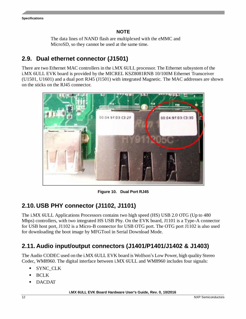
2.9. Dual ethernet connector (J1501)
There are two Ethernet MAC controllers in the i.MX 6ULL processor. The Ethernet subsystem of the
i.MX 6ULL EVK board is provided by the MICREL KSZ8081RNB 10/100M Ethernet Transceiver
(U1501, U1601) and a dual port RJ45 (J1501) with integrated Magnetic. The MAC addresses are shown
on the sticks on the RJ45 connector.
Figure 10. Dual Port RJ45
2.10. USB PHY connector (J1102, J1101)
The i.MX 6ULL Applications Processors contains two high speed (HS) USB 2.0 OTG (Up to 480
Mbps) controllers, with two integrated HS USB Phy. On the EVK board, J1101 is a Type-A connector
for USB host port, J1102 is a Micro-B connector for USB OTG port. The OTG port J1102 is also used
for downloading the boot image by MFGTool in Serial Download Mode.
2.11. Audio input/output connectors (J1401/P1401/J1402 & J1403)
The Audio CODEC used on the i.MX 6ULL EVK board is Wolfson’s Low Power, high quality Stereo
Codec, WM8960. The digital interface between i.MX 6ULL and WM8960 includes four signals:
• SYNC_CLK
• BCLK
• DACDAT

Specifications
i.MX 6ULL EVK Board Hardware User's Guide, Rev. 0, 10/2016
NXP Semiconductors 13
• ADCDAT
i.MX 6ULL also provides the MCLK to WM8960.
i.MX 6ULL EVK includes one headphone interface (J1401), one onboard MIC (P1401), and two
speaker interfaces (J1402, J1403). J1401 is a 3.5 mm 4-pole (or TRRS) phone jack, which supports jack
detect.
2.12. USB debug connector (J1901)
On the EVK board, CP2102, a USB to Serial UART IC is used to convert the UART signal to the USB
signal. With the Micro-B USB connector J1901, the connection for debugging is simplified. A Micro-B to
standard A USB cable can be used.
UART1 port is used as the default debug port. No RTS or CTS signals are sent from the processor to the
debug connector because these signals are commonly ignored by most applications. The required terminal
settings are shown in the following table.
Table 5. Terminal settings
Baud rate 115,200
Data bits 8
Parity None
Stop bits 1
Flow control None
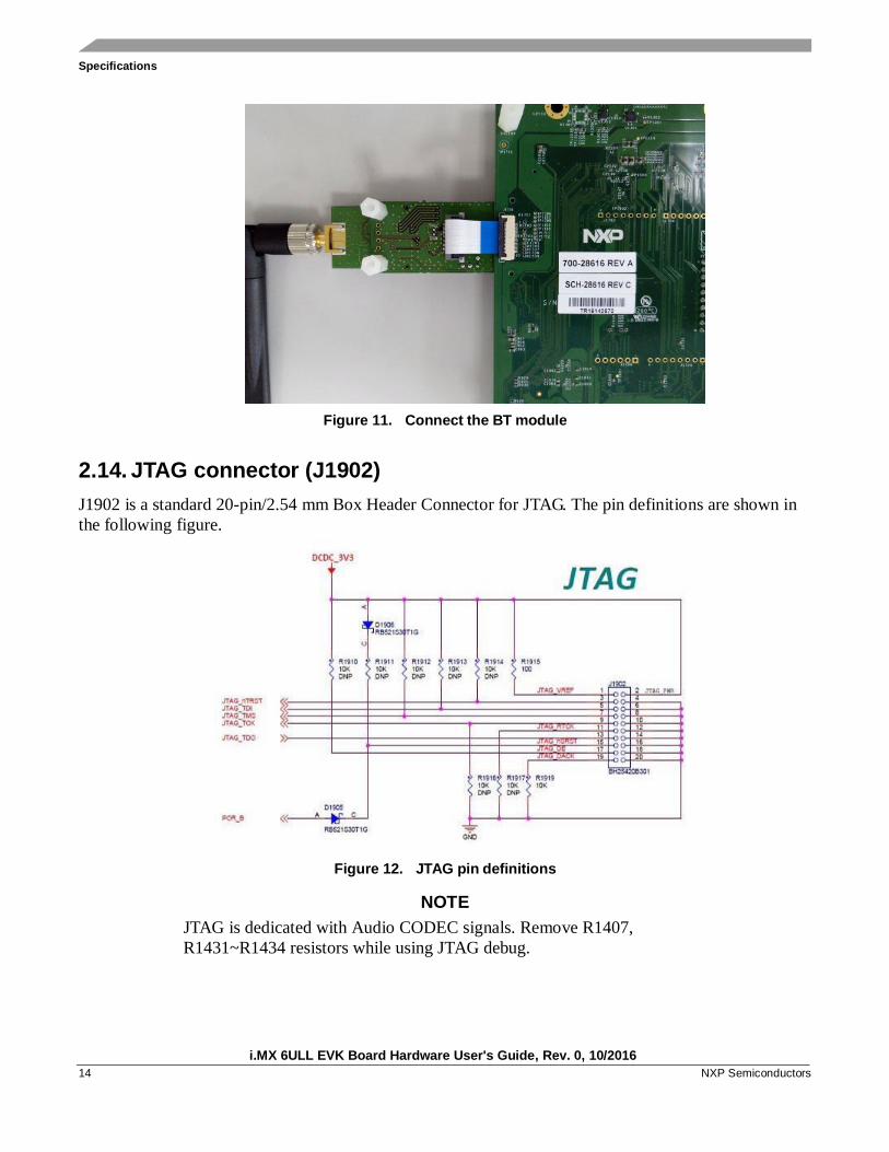
2.13. Bluetooth Connector (J1701)
On the EVK board, the J1701 is connected to i.MX 6ULL UART2 port, and can be used for Bluetooth.
Silex Bluetooth module SX-SDCAN-2830BT is recommended. To verify other Bluetooth modules, a
convert board may be needed.
NOTE
J1701 is a bottom-contact type connector for BT connection on the Rev. C
board. 20-pin/0.5 mm pitch same side FFC/FPC should be used to connect
with Silex Bluetooth module SX-SDCAN-2830BT, as shown in the
following figure.
Specifications
i.MX 6ULL EVK Board Hardware User's Guide, Rev. 0, 10/2016
14 NXP Semiconductors
Figure 11. Connect the BT module
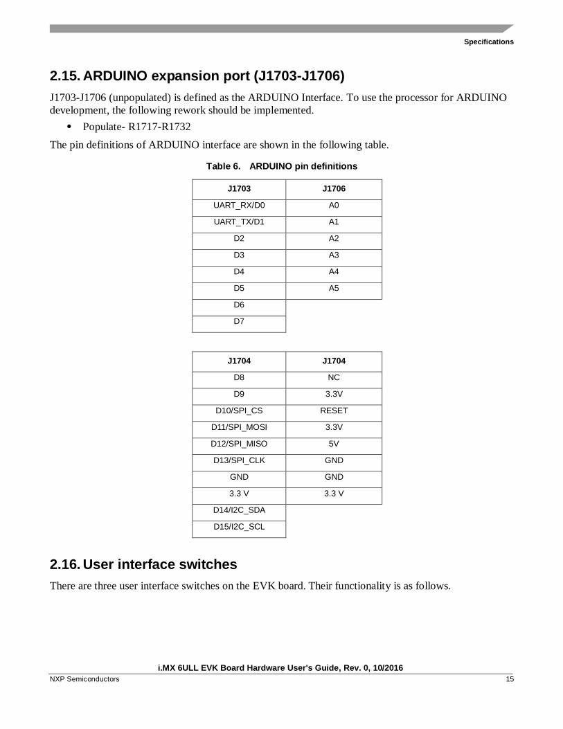
2.14. JTAG connector (J1902)
J1902 is a standard 20-pin/2.54 mm Box Header Connector for JTAG. The pin definitions are shown in
the following figure.
Figure 12. JTAG pin definitions
NOTE
JTAG is dedicated with Audio CODEC signals. Remove R1407,
R1431~R1434 resistors while using JTAG debug.
Specifications
i.MX 6ULL EVK Board Hardware User's Guide, Rev. 0, 10/2016
NXP Semiconductors 15
2.15. ARDUINO expansion port (J1703-J1706)
J1703-J1706 (unpopulated) is defined as the ARDUINO Interface. To use the processor for ARDUINO
development, the following rework should be implemented.
• Populate- R1717-R1732
The pin definitions of ARDUINO interface are shown in the following table.
Table 6. ARDUINO pin definitions
J1703 J1706
UART_RX/D0 A0
UART_TX/D1 A1
D2 A2
D3 A3
D4 A4
D5 A5
D6
D7
J1704 J1704
D8 NC
D9 3.3V
D10/SPI_CS RESET
D11/SPI_MOSI 3.3V
D12/SPI_MISO 5V
D13/SPI_CLK GND
GND GND
3.3 V 3.3 V
D14/I2C_SDA
D15/I2C_SCL
2.16. User interface switches
There are three user interface switches on the EVK board. Their functionality is as follows.
Specifications
i.MX 6ULL EVK Board Hardware User's Guide, Rev. 0, 10/2016
16 NXP Semiconductors
2.16.1. ON/OFF button (SW2101)
SW2101 is the ON/OFF button for the i.MX 6ULL EVK board. The function of this button is listed below.
• In Yocto Project, short press and long press will only generate an interrupt, the usage is defined
by upper software.
• Prolonged depress (>5 sec) will force an immediate hardware shutdown.
• If the board is in SHUTDOWN state, a short press of the button will restart (boot) the system.
• If the board is in STANDBY state, a short press of the button will bring the system out of
standby (resume operations, no boot).
2.16.2. Reset
There are two ways to reset the i.MX6ULL EVK board:
1. Hardware way to reset system using SW2102:
— Pressing the RESET button (SW2102) in the Power On state will force to reset almost all
the power rails except the VDD_SNVS on the i.MX6ULL EVK board. The i.MX6ULL
applications processor will be immediately turn off, and reinitiate a boot cycle from the
Processor Power Off state.
2. Software way to reset system using WDOG signal:
— When system assert nWDOG signal, U703 will be shut down, and the system will power
down, and then nWDOG is released, then U703 will be power on by PMIC_ON_REQ, the
system will then reboot. It is important that the system reset should be power down and
then power on, which will avoid boot failure caused by DVFS or DRAM (LPDDR2 if
used).
2.16.3. Power switch (SW2001)
SW2001 is a slide switch to control the power of the i.MX 6ULL EVK board. The function of this
switch is listed below.
• Sliding the switch to the ON position connects the 5 V power supply to the Evaluation board main
power system.
• Sliding the switch to OFF position immediately removes all power from the board.
2.17. Sensors
The i.MX 6ULL EVK board has three sensors: Accelerometer (FXLS8471Q), eCOMPASS (MAG3110),
and Gyroscope (FXAS21002CQ, unpopulated). These three sensors are connected to the i.MX 6ULL
I2C1 port.
Specifications
i.MX 6ULL EVK Board Hardware User's Guide, Rev. 0, 10/2016
NXP Semiconductors 17
2.17.1. Accelerometer
FXLS8471Q is a small, low-power, 3-axis, linear accelerometer in a 3 mm x 3 mm x 1 mm QFN package.
FXLS8471Q has dynamically selectable acceleration full-scale ranges of ±2 g/±4 g/±8 g and 14 bits of
resolution.
2.17.2. eCOMPASS (U1302)
MAG3110 is a small, low-power, 3-axis digital magnetometer. It works by measuring the strength of a
magnetic field, which is a combination of earth’s magnetic field and the magnetic fields of nearby objects,
including distortions. The device can be used in conjunction with a 3-axis accelerometer to produce
orientation-independent, accurate compass heading information.
2.17.3. Gyroscope (U1303)
FXAS21002CQ is a small, low-power, yaw, pitch, and roll angular rate gyroscope with 16-bit ADC
resolution. The full-scale range is adjustable from 250/s to 2000/s. It is not populated by default, to
verify this feature the chip must first be purchased and soldered.
2.18. User interface LED indicators
There are two LED status indicators located on the board. The functions of these LEDs include:
• Main Power Supply (D2003)
— Green: DC 5 V main supply (WALL_5V_DC_JACK) is normal.
— Red: WALL_5V_DC_JACK is over 5.6 V.
— Off: the board is not powered.
• UART (D1903)
— Green flashing: Debug UART data are being transmitted to PC.
— Orange flashing: Debug UART data are being received from PC.
2.19. Optional back-up coin cell holder (BT2101)
On the i.MX 6ULL EVK board, there is a connector (BT2101) for holding an ML414 Lithium coin cell
battery. The coin cell provides an alternative power supply for i.MX 6ULL VDD_SNVS_IN power rail
when the main VDD_SNVS_3V3 is off. When VDD_SNVS_3V3 is on, the coin cell can be charged
through a current limit resistor R101. i.MX 6ULL has an internal LDO to regulate the VDD_SNVS_IN
power to supply the RTC subsystem. When DC 5 V power supply is removed, the coin cell will provide
power only to the VDD_SNVS_IN power rail of the EVK board. To increase the keep time of RTC, the
developer should optimize the power consumption of the whole VDD_SNVS_IN power rail.
2.20. LCD daughter card
If developers want to use LCD, NXP provides an optional LCD module LCD8000-43T which has a 4.3-
inch touch-screen and supports a resolution of up to 480X3(RGB)X272. This module contains a 50-pin
Contents of the Evaluation Kit
i.MX 6ULL EVK Board Hardware User's Guide, Rev. 0, 10/2016
18 NXP Semiconductors
FPC cable, which can be inserted to connector J901 on the base board (the bottom contact). LCD
modules can be purchased from the NXP website.
3. PCB Information
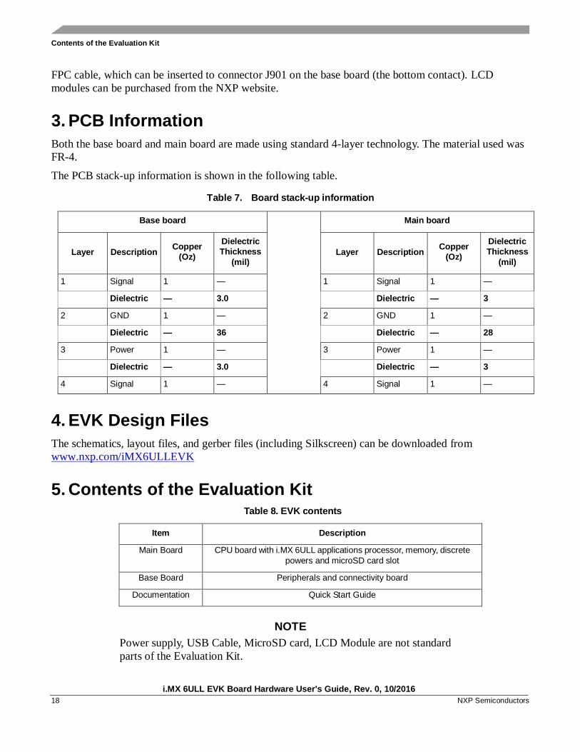
Both the base board and main board are made using standard 4-layer technology. The material used was
FR-4.
The PCB stack-up information is shown in the following table.
Table 7. Board stack-up information
Base board Main board
Layer
Description
Copper
(Oz)
Dielectric
Thickness
(mil)
Layer
Description
Copper
(Oz)
Dielectric
Thickness
(mil)
1 Signal 1 — 1 Signal 1 —
Dielectric — 3.0 Dielectric — 3
2 GND 1 — 2 GND 1 —
Dielectric — 36 Dielectric — 28
3 Power 1 — 3 Power 1 —
Dielectric — 3.0 Dielectric — 3
4 Signal 1 — 4 Signal 1 —
4. EVK Design Files
The schematics, layout files, and gerber files (including Silkscreen) can be downloaded from
www.nxp.com/iMX6ULLEVK
5. Contents of the Evaluation Kit Table 8. EVK contents
Item Description
Main Board CPU board with i.MX 6ULL applications processor, memory, discrete
powers and microSD card slot
Base Board Peripherals and connectivity board
Documentation Quick Start Guide
NOTE
Power supply, USB Cable, MicroSD card, LCD Module are not standard
parts of the Evaluation Kit.
Revision History
i.MX 6ULL EVK Board Hardware User's Guide, Rev. 0, 10/2016
NXP Semiconductors 19
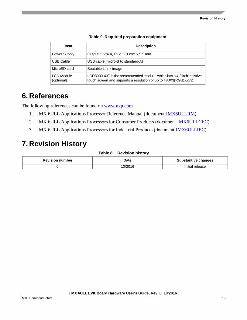
Table 9. Required preparation equipment
Item Description
Power Supply Output: 5 V/4 A, Plug: 2.1 mm x 5.5 mm
USB Cable USB cable (micro-B to standard-A)
MicroSD card Bootable Linux image
LCD Module
(optional) LCD8000-43T is the recommended module, which has a 4.3-inch resistive
touch screen and supports a resolution of up to 480X3(RGB)X272.
6. References
The following references can be found on www.nxp.com
1. i.MX 6ULL Applications Processor Reference Manual (document IMX6ULLRM)
2. i.MX 6ULL Applications Processors for Consumer Products (document IMX6ULLCEC)
3. i.MX 6ULL Applications Processors for Industrial Products (document IMX6ULLIEC)
7. Revision History Table 8. Revision history
Revision number Date Substantive changes
0 10/2016 Initial release

Document Number: IMX6ULLEVKHUG Rev. 0
10/2016
How to Reach Us:
Home Page:
nxp.com
Web Support:
nxp.com/support
Information in this document is provided solely to enable system and software
implementers to use NXP products. There are no express or implied copyright licenses
granted hereunder to design or fabricate any integrated circuits based on the
information in this document. NXP reserves the right to make changes without further
notice to any products herein.
NXP makes no warranty, representation, or guarantee regarding the suitability of its
products for any particular purpose, nor does NXP assume any liability arising out of
the application or use of any product or circuit, and specifically disclaims any and all
liability, including without limitation consequential or incidental damages. “Typical”
parameters that may be provided in NXP data sheets and/or specifications can and do
vary in different applications, and actual performance may vary over time. All operating
parameters, including “typicals,” must be validated for each customer application by
customer’s technical experts. NXP does not convey any license under its patent rights
nor the rights of others. NXP sells products pursuant to standard terms and conditions
of sale, which can be found at the following address:
nxp.com/SalesTermsandConditions.
NXP, the NXP logo, NXP SECURE CONNECTIONS FOR A SMARTER WORLD,
Freescale, the Freescale logo, and Kinetis are trademarks of NXP B.V. All other
product or service names are the property of their respective owners.
ARM, the ARM Powered logo, and Cortex are registered trademarks of ARM Limited (or
its subsidiaries) in the EU and/or elsewhere. All rights reserved.
© 2016 NXP B.V.