in this issue 2 editors’ notes; new product introductions ... issn 0161-3626 ©analog devices,...
TRANSCRIPT

wwwanalogcomanalogdialogue
In This Issue 2 Editorsrsquo Notes New Product Introductions
3 PLC Evaluation Board Simplifies Design of Industrial Process-Control Systems
11 Skin Impedance Analysis Aids Active and Passive Transdermal Delivery
13 AccelerometersmdashFantasy and Reality
15 Digital Isolator Simplifies USB Isolation in Medical and Industrial Applications
19 Automated Calibration Technique Reduces DAC Offset to Less Than 1 mV
21 ldquoRules of the Roadrdquo for High-Speed Differential ADC Drivers
Volume 43 Number 2 2009 A forum for the exchange of circuits systems and software for real-world signal processing
2 ISSN 0161-3626 copyAnalog Devices Inc 2010
Editorsrsquo NotesIN THIS ISSUE
PLC Evaluation Board Simplifies Design of Industrial Process-Control SystemsThe applications for industr ial process-control systems range from simple traf f ic control to complex electr ical power grids from environmental control systems to oil-ref inery process control The intelligence of these systems lies in their measurement and control units The two most common computer-based systems to control machines and processes are programmable log ic control lers and distributed control systems Page 3
Skin Impedance Analysis Aids Active and Passive Transdermal DeliveryPhar maceut ica l f i r ms a re developing a lter nat ives to injections Transdermal methods which feature noninvasive delivery of medication through a patientrsquos skin overcome the protective barrier in one of two ways passive absorption and active penetration Skin impedance analysis facilitates proper dosing Page 11
AccelerometersmdashFantasy and Reality High sensitivity small size low cost rugged packaging and the ability to measure both static and dynamic acceleration have made numerous new applications of surface micromachined accelerometers possible Many of these were not anticipated because they were not thought of as classic accelerometer applicat ions New applicat ions are l imited only by the imagination of designers Page 13
Digital Isolator Simplifies USB Isolation in Medical and Industrial ApplicationsDespite its low speed and point-to-point nature RS-232 was tolerated in medical and industrial applications because it was universally available well supported and allowed easy implementation of the required isolation The ADuM4160 digital isolator allows simple inexpensive isolation of full- and low-speed USB peripheralsmdashincluding the D+ and Dndash linesmdashincreasing the usefulness of USB in medical and industrial applications Page 15
Automated Calibration Technique Reduces DAC Offset to Less Than 1 mVThe AD5360 16-bit 16-channel DAC is factory trimmed but an offset of several millivolts can still exist This idea shows how a simple software algorithm can reduce an unknown offset to less than 1 mV This technique can be used for factory calibration or for offset correction at any point in the DACrsquos life cycle Page 19
ldquoRules of the Roadrdquo for High-Speed Differential ADC Drivers Most modern high-performance ADCs use differential inputs to reject common-mode noise and interference increase dynamic range by a factor of two and improve overall per formance ADC dr iversmdashcircuits of ten speci f ical ly designed to provide dif ferential signalsmdashperform many important functions including amplitude scaling single-ended-to-differential conversion buffering common-mode offset adjustment and filtering Page 21
Dan Sheingold [dansheingoldanalogcom]
Scott Wayne [scottwayneanalogcom]
Analog Dialogue wwwanalogcomanalogdialogue the technical magazine of Analog Devices discusses products applications technology and techniques for analog digital and mixed-signal processing Published continuously for 43 yearsmdashstarting in 1967mdashit is currently available in two versions Monthly editions offer technical articles timely information including recent application notes new-product briefs pre-release products webinars and tutorials and published articles and potpourri a universe of links to important and relevant information on the Analog Devices website wwwanalogcom Printable quarterly issues feature collections of monthly articles For history buffs the Analog Dialogue archive includes all regular editions starting with Volume 1 Number 1 (1967) and three special anniversary issues If you wish to subscribe please go to wwwanalogcomanalogdialoguesubscribehtml Your comments are always welcome please send messages to dialogueeditoranalogcom or to Dan Sheingold Editor [dansheingoldanalogcom] or Scott Wayne Publisher and Managing Editor [scottwayneanalogcom]
PRODUCT INTRODUCTIONS VOLUME 43 NUMBER 2Data sheets for all ADI products can be found by entering the part
number in the search box at wwwanalogcom
AprilDAC current-output 14-bit 2500-MSPS AD9739Multiplexer iCMOS 41 1-Ω ADG1604Switch iCMOS dual SPDT 1-Ω ADG1636Switches iCMOS quad SPST 1-Ω ADG14611ADG1612ADG1613
MayAccelerometer gyroscope and magnetometer 3-axis ADIS16405Buffer clock ultrafast 2-input 12-output ADCLK954Comparator voltage very fast LVDS AD8465Controller touch-screen low-voltage AD7889DACs current-output 12-16-bit AD5410AD5420DAC voltage-output quad 12-bit AD5724REnergy Meters single-phase ADE5566ADE5569Gyroscope yaw-rate ADXRS622
JuneAccelerometer gyroscope and magnetometer 3-axis ADIS16400Amplifier audio Class-D 2 times 2-W SSM2356 Amplifier difference unity-gain wide supply range AD8276Amplifier instrumentation micropower AD8236Amplifier operational dual wideband ADA4692-2Amplifiers RFIF ultralow-distortion ADL5561ADL5562Amplifier variable-gain 1 MHz to 12 GHz ADL5331Amplifier variable-gain quad 235-MHz AD8264ADC pipelined quad 12-bit 170-MSPS210-MSPS AD9639ADC sum-∆ 24-bit 48-kHz AD7192ADC sum-∆ 24-bit programmable gain data rate AD7191ADC successive-approximation 18-bit 2-MSPS AD7986ADC successive-approximation dual 14-bit 42-MSPS AD7357ADCs pipelined dual 14-16-bit 125-MSPS AD9258AD9268ADCs sum-∆ 24-20-bit pin-programmable AD7780AD7781Buffer clock fanout 6 LVPECL outputs ADCLK946Buffer clock fanout 12 LVDS24 CMOS outputs ADCLK854Controller digital isolated power supplies ADP1043Converter dc-to-dc step-down 600 mA ADP2109 Converter dc-to-dc synchronous step-down 600 mA ADP2121Converters dc-to-dc step-up 650 kHz1300 kHz ADP1612ADP1613DAC RF 14-bit 2400-MSPS 4-channel QAM AD9789DACs current- and voltage output 12-16-bit AD5412AD5422Detector rms power 50-dB 50 Hz to 6 GHz AD8363Driver 7-channel LED ADP8860Drivers differential ADC single and dual ADA4950-1ADA4950-2Generator multiservice clock AD9551Generatorsynchronizer network clock AD9548Isolators digital 4-channel 5-kV ADuM4400ADuM4401ADuM4402Microcontroller precision analog two 24-bit ADCs ADuC7060Potentiometers digital 256-1024-position AD5291AD5292Potentiometer digital 1024-position AD5293Processor digital audio flexible routing matrix ADAU1446Processors embedded Blackfin ADSP-BF52xADSP-BF52xCPower Management Unit imaging ADP5020Sensor impact programmable ADIS16240 Sensors temperature 16-bit ADT7310ADT7410Tuner mobile TV ISDB-T ADMTV202
Analog Dialogue Volume 43 Number 2 3
PLC Evaluation Board Simplifies Design of Industrial Process-Control SystemsBy Colm Slattery Derrick Hartmann and Li Ke
IntroductionThe applications for industrial process-control systems are diverse ranging from simple traffic control to complex electrical power grids from environmental control systems to oil-refinery process control The intelligence of these automated systems lies in their measurement and control units The two most common computer-based systems to control machines and processes dealing with the various analog and digital inputs and outputs are programmable logic controllers1 (PLCs) and distributed control systems2 (DCSrsquos) These systems comprise power supplies central processor units (CPUs) and a variety of analog-input analog-output digital-input and digital-output modules
The standard communications protocols have existed for many years the ranges of analog variables are dominated by 4 mA to 20 mA 0 V to 5 V 0 V to 10 V plusmn5 V and plusmn10 V There has been much discussion about wireless solutions for next-generation systems but designers still claim that 4 mA to 20 mA communications and control loops will continue to be used for many years The criteria for the next generation of these systems will include higher performance smaller size better system diagnostics higher levels of protection and lower costmdashall factors that will help manufacturers differentiate their equipment from that of their competitors
We will discuss the key performance requirements of process-control systems and the analog inputoutput modules they containmdashand will introduce an industrial process-control evaluation system that integrates these building blocks using the latest integrated-circuit technology We also look at the challenges of designing a robust system that will withstand the electrical fast transients (EFTs) electrostatic discharges (ESDs) and voltage surges found in industrial environmentsmdashand present test data that verifies design robustness
PLC Overview with Application ExampleFigure 1 shows a basic process-control system building block A process variable such as flow rate or gas concentration is monitored via the input module The information is processed by the central control unit and some action is taken by the output module which for example drives an actuator
ACTUATORS
INPUTMODULE(S)
CENTRALCONTROL UNIT
OUTPUTMODULE(S)
SENSORS
PLCPROGRAM
Figure 1 Typical top-level PLC system
Figure 2 shows a typical industrial subsystem of this type Here a CO2 gas sensor determines the concentration of gas accumulated in a protected area and transmits the information to a central control point The control unit consists of an analog input module that conditions the 4 mA to 20 mA signal from the sensor a central processing unit and an analog output module that controls the required system variable The current loop can handle large
capacitive loadsmdashoften found on hundreds-of-meters long communications paths experienced in some industrial systems The output of the sensor element representing gas concentration levels is transformed into a standard 4 mA to 20 mA signal which is transmitted over the current loop This simplified example shows a single 4 mA to 20 mA sensor output connected to a single-channel input module and a single 0 V to 10 V output In practice most modules have multiple channels and configurable ranges
The resolution of inputoutput modules typically ranges from 12- to 16 bits with 01 accuracy over the industrial temperature range Input ranges can be as small as plusmn10 mV for bridge transducers and as large as plusmn10 V for actuator controllersmdashor 4 mA to 20 mA currents in process-control systems Analog output voltage and current ranges typically include plusmn5 V plusmn10 V 0 V to 5 V 0 V to 10 V 4 mA to 20 mA and 0 mA to 20 mA Settling-time requirements for digital-to-analog converters (DACs) vary from 10 μs to 10 ms depending on the application and the circuit load
0V TO 10V
4mA TO 20mA
CPU
OUTPUT MODULE
INPUT MODULE
RACK
GASSENSOR
Figure 2 Gas sensor
The 4 mA to 20 mA range is mapped to represent the normal gas detection range current values outside this range can be used to provide fault-diagnostic information as shown in Table 1
Table 1 Assigning Currents Outside the 4 mA to 20 mA Output Range
Current Output (mA) Status00 Unit fault08 Unit warm-up12 Zero drift fault16 Calibration fault20 Unit spanning22 Unit zeroing4 to 20 Normal measuring mode40 Zero gas level56 10 full scale80 25 full scale12 50 full scale16 75 full scale20 Full scalegt20 Overrange
PLC Evaluation SystemThe PLC evaluation system3 described here integrates all the stages needed to generate a complete inputoutput design It contains four fully isolated ADC channels an ARM7trade microprocessor with RS-232 interface and four fully isolated DAC output channels The board is powered by a dc supply Hardware-configurable input ranges include 0 V to 5 V 0 V to 10 V plusmn5 V plusmn10 V 4 mA to 20 mA 0 mA to 20 mA plusmn20 mA as well as thermocouple and RTD Software-programmable output ranges include 0 V to 5 V 0 V to 10 V plusmn5 V plusmn10 V 4 mA to 20 mA 0 mA to 20 mA and 0 mA to 24 mA
4 Analog Dialogue Volume 43 Number 2
ANALOG SIGNALS
SENSOR INPUTSbullRTDbullTCbullGAS
VOLTAGE INPUTS(FLOW PRESSURE)
bull0V TO 5V 0V TO 10Vbull 5V 10V
CURRENT INPUTS(COMMUNICATIONS)
bull0mA TO 24mAbull4mA TO 20mA
ANALOG OUTPUTS
VOLTAGE OUTPUTSbull0V TO 5V 0V TO 10Vbull 5V 10V
CURRENT OUTPUTSbull0mA TO 24mAbull4mA TO 20mA
ANALOG INPUTOUTPUT MODULE
PLC MODULEBOARD
Figure 3 Analog inputoutput module
Output Module Table 2 highlights some key specifications of PLC output modules Since the true system accuracy lies within the measurement channel (ADC) the control mechanism (DAC) requires only enough resolution to tune the output For high-end systems 16-bit resolution is required This requirement is actually quite easy to satisfy using standard digital-to-analog architectures Accuracy is not crucial 12-bit integral nonlinearity (INL) is generally adequate for high-end systems
Calibrated accuracy of 005 at 25degC is easily achievable by overranging the output and trimming to achieve the desired value Todayrsquos 16-bit DACs such as the AD50664 offer 005 mV typical offset error and 001 typical gain error at 25degC eliminating the need for calibration in many cases Total accuracy error of 015 sounds manageable but is actually quite aggressive when specified over temperature A 30 ppmdegC output drift can add 018 error over the industrial temperature range
Table 2 Output Module SpecificationsSystem Specification RequirementResolution 16 bitsCalibrated Accuracy 005Total Module Accuracy Error 015Open-Circuit Detection YesShort-Circuit Detection YesShort-Circuit Protection YesIsolation Yes
Output modules may have current outputs voltage outputs or a combination A classical solution that uses discrete components to implement a 4 mA to 20 mA loop is shown in Figure 4 The AD5660 16-bit nanoDACreg converter provides a 0 V to 5 V output that sets the current through sense resistor RS and therefore through R1 This current is mirrored through R2
Setting RS = 15 kΩ R1 = 3 kΩ R2 = 50 Ω and using a 5-V DAC will result in IR2 = 20 mA max
VDD
AD566016-BITDAC
25VREF
AMPAMP
R1
RS
R2
VDD
TERMINALSCREWS
VDAC
4mA TO 20mA
Figure 4 Discrete 4 mA to 20 mA implementation
This discrete design suffers from many drawbacks Its high component count engenders significant system complexity board size and cost Calculating total error is difficult with multiple components adding varying degrees of error with coefficients that can be of differing polarities The design does not provide short-circuit detectionprotection or any level of fault diagnostics It does not include a voltage output which is required in many industrial control modules Adding any of these features would increase the design complexity and the number of components A better solution would be to integrate all of the above on a single IC such as the AD5412AD5422 low-cost high-precision 12-16-bit digital-to-analog converters They provide a solution that offers a fully integrated programmable current source and programmable voltage output designed to meet the requirements of industrial process-control applications
LATCH
CLEAR
CLEARSELECT
SCLK
SDIN
SDO
INPUTSHIFT
REGISTERAND
CONTROL
POWERON
RESET
16-BITDAC
16
R1
R2 R3BOOST
AVDDAVSS
REFIN GND CCOMP2 CCOMP1
DVSSDVCC SELECT
IOUT
FAULT
RANGESCALING
REFOUT
VREF +VSENSE
RSET
VOUT
ndashVSENSE
AD5422
Figure 5 AD5422 programmable voltagecurrent output
The output current range is programmable to 4 mA to 20 mA 0 mA to 20 mA or 0 mA to 24 mA overrange function A voltage output available on a separate pin can be configured to provide 0 V to 5 V 0 V to 10 V plusmn5 V or plusmn10 V ranges with a 10 overrange available on all ranges Analog outputs are short-circuit protected a critical feature in the event of miswired outputsmdashfor example when the user connects the output to ground instead of to the load The AD5422 also has an open-circuit detection feature that monitors the current-output channel to ensure that no fault has occurred between the output and the load In the event of an open circuit the FAULT pin will go active alerting the system controller The AD5750 programmable currentvoltage output driver features both short-circuit detection and protection
Analog Dialogue Volume 43 Number 2 5
Figure 6 shows the output module used in the PLC evaluation system While earlier systems typically needed 500 V to 1 kV of isolation today gt2 kV is generally required The ADuM1401 digital isolator uses iCouplerreg5 technology to provide the necessary isolation between the MCU and remote loads or between the inputoutput module and the backplane Three channels of the ADuM1401 communicate in one direction the fourth channel communicates in the opposite direction providing isolated data readback from the converters For newer industrial designs the ADuM3401 and other members of its family of digital isolators provide enhanced system-level ESD protection
The AD5422 generates its own logic supply (DVCC) which can be directly connected to the field side of the ADuM1401 eliminating the need to bring a logic supply across the isolation barrier The AD5422 includes an internal sense resistor but an external resistor (R1) can be used when lower drift is required Because the sense resistor controls the output current any drift of its resistance will affect the output The typical temperature coefficient of the internal sense resistor is 15 ppmdegC to 20 ppmdegC which could add 012 error over a 60degC temperature range In high-performance system applications an external 2-ppmdegC sense resistor could be used to keep drift to less than 0016
The AD5422 has an internal 10-ppmdegC max voltage reference that can be enabled on all four output channels in the PLC evaluation system Alternatively the ADR445 ultralow-noise XFETreg voltage reference with its 004 initial accuracy and 3 ppmdegC can be used on two output channels allowing performance comparison and a choice of internal vs external reference depending on the total required system performance
Input Module The input module design specifications are similar to those of the output module High resolution and low noise are
generally important In industrial applications a differential input is required when measuring low-level signals from thermocouples strain gages and bridge-type pressure sensors to reject common-mode interference from motors ac power lines or other noise sources that inject noise into the analog inputs of the analog-to-digital converter (ADCs)
Sigma-delta ADCs are the most popular choice for input modules as they provide high accuracy and resolution In addition internal programmable-gain amplifiers (PGAs) allow small input signals to be measured accurately Figure 7 shows the input module design used in the evaluation system The AD7793 3-channel 24-bit sigma-delta ADC is configured to accommodate a large range of input signals such as 4 mA to 20 mA plusmn10 V as well as small signal inputs directly from sensors
Care was taken to allow this universal input design to be easily adapted for RTDthermocouple modules As shown two input terminal blocks are provided per input channel One input allows for a direct connection to the AD7793 The user can program the internal PGA to provide analog gains up to 128 The second input allows the signal to be conditioned through the AD8220 JFET-input instrumentation amplifier In this case the input signal is attenuated amplified and level shifted to provide a single-ended input to the ADC In addition to providing the level shifting function the AD8220 also features very good common-mode rejection important in applications having a wide dynamic range
The low-power high-performance AD7793 consumes lt500 μA and the AD8220 consumes lt750 μA This channel is designed to accept 4 mA to 20 mA 0 V to 5 V and 0 V to 10 V analog inputs Other channels in the input module have been designed for bipolar operation to accept plusmn5 V and plusmn10 V input signals
ISO
10 F01 F
VOUT
IOUT
GNDISO
ISOISO
01
F
ISO
ISO
10 F 01 FVDD1 VDD2GND1 GND2VIA VOAVIB VOBVIC VOCVOD VIDENO1 ENO2GND1 GND2
ADuM1401TPVINNCGND
TPNC
VOUTTRIM
ADR445
DVCC AVSS AVDD
RSET VREF
LATCHSCLKSDINSDOUT
AD5422VOUT
IOUT
(ISOLATED)
ndash15VISO GNDISO +15VISO
R115k
Figure 6 Output module block level
VDD
VREF
ISOISO
ISO
VDDISO VDD1GNDISO GND1VOA VIAVOB VIBVOC VICVID
CSSCLK
DINDOUTRDY VOD
VSEL RCOUTGNDISO GND1
ADuM5401
AIN+AD7793
AINndash
ISO
ISOISO
S4S1
S3
S2
AD8220
VDDISO
REF
+RGRG
ndash15k250
AIN1+
AIN1ndash
VIN
GND
ISO
01 F 01 F10 F
VDDISO 20k
51k
ADR441VIN VOUT
ISO ISO ISO
VDDISO
AD8601
VDDISO VDDISO
Figure 7 Input module design
6 Analog Dialogue Volume 43 Number 2
To measure a 4 mA to 20 mA input signal a low-drift precision resistor can be switched (S4) into the circuit In this design its resistance is 250 Ω but any value can be used as long as the generated voltage is within the input range of the AD8220 S4 is left open when measuring a voltage
Isolation is required for most input-module designs Figure 7 shows how isolation was implemented on one channel of the PLC evaluation system The ADuM5401 4-channel digital isolator uses isoPowerreg6 technology to provide 25-kV rms signal and power isolation In addition to providing four isolated signal channels the ADuM5401 also contains an isolated dc-to-dc converter that provides a regulated 5-V 500-mW output to power the analog circuitry of the input module
Complete System An overview of the complete system is shown in Figure 8 The ADuC7027 precision analog microcontroller7 is the main system controller Featuring the ARM7TDMIreg core its 32-bit architecture allows easy interface to 24-bit ADCs It also supports a 16-bit thumb mode which allows for greater code density if required The ADuC7027 has 16 kB of on-board flash memory and allows interfacing to up to 512 kB external memory The ADP3339 high-accuracy low-dropout regulator (LDO) provides the regulated supply to the microcontroller
Communication between the evaluation board and the PC is provided via the ADM3251E isolated RS-232 transceiver The ADM3251E incorporates isoPower technologymdashmaking a separate isolated dc-to-dc converter unnecessary It is ideally suited to operation in electrically harsh environments or where RS-232 cables are frequently plugged in or unplugged as the RS-232 pins Rx and Tx are protected against electrostatic discharges of up to plusmn15 kV
Evaluation System Software and Evaluation Tools The evaluation system is very versatile Communication with the PC is achieved using LabVIEWtrade8 The firmware for the microcontroller (ADuC7027) is written in C which controls the low-level commands to and from the ADC and DAC channels
Figure 9 shows the main screen interface Pull-down menus on the left side allow the user to choose active ADC and DAC channels Under each ADC and DAC menu there is a pull-down range menu which is used to select the desired input and output ranges to be measured and controlled The following input and output ranges are available 4 mA to 20 mA 0 mA to 20 mA 0 mA to 24 mA 0 V to 5 V 0 V to 10 V plusmn5 V and plusmn10 V Small signal input ranges can also be accommodated directly on the ADC by using its internal PGA
Figure 9 Evaluation software main screen controller
AD7793 ADuM1401
ISOLATED
BIPOLARISOLATEDDC-TO-DC
AD8220
ADR441IOUT1
IOUT2
+5V
RREF
15VVI INPUTS BIPOLAR SUPPLY HIGH PERFORMANCE
AD7793
ADuM5401
ISOLATEDAD8220
IOUT1
IOUT2RREF
VI INPUTS SINGLE SUPPLY LOWER COST
+24V
+24V
+5V
SPI
AD
uC70
27A
DP3
339
ISODC-TO-DC
AD5422
IOUTRANGESCALE
VOUTRANGESCALE
DAC
SPI
OVERTEMPDETECT
OPENDETECT
4mA TO 20mA0mA TO 24mA
0V TO 5V 0V TO 10V
5V 10V
ADuM1401
ISOLATED
ADR445ISO
DC-TO-DC15V
(gt30mA)
+33V
AD5422
IOUTRANGESCALE
VOUTRANGESCALE
DAC
REF
SPI
OVERTEMPDETECT
OPENDETECT
4mA TO 20mA0mA TO 24mA
0V TO 5V 0V TO 10V
5V 10V
ADuM1401
ISOLATED
(gt30mA)ISO DC-TO-DC 15V
+5V
+5VADM3251EISOLATED
RS-232TxRx
Figure 8 System-level design
Analog Dialogue Volume 43 Number 2 7
The ADC Configure screen shown in Figure 10 is used to set the ADC channel update rate and PGA gain to enable or disable excitation currents and for other general-purpose ADC settings Each ADC channel is calibrated by connecting the corresponding DAC output channel to the ADC input terminal and adjusting each range When using this method of calibration therefore the offset and gain errors of the AD5422 dictate the offset and gain of each channel If these provide insufficient accuracy ultrahigh-precision current and voltage sources can be used for calibration if desired
Figure 10 ADC Configure screen
After selecting the ADCrsquos input channel input range and update rate we can now use the ADC Stats screen shown in Figure 11 to display some measured data On this screen the user chooses the number of data points to record the software generates a histogram of the selected channel calculates the peak-to-peak and rms noise and displays the results In the measurement shown here the input is connected through the AD8220 to the AD7793 gain = 1 update rate = 167 Hz number of samples = 512 input range = plusmn10 V input voltage = 25 V The peak-to-peak resolution is 182 bits
Figure 11 ADC Stats screen
In Figure 12 the input is connected directly to the AD7793 bypassing the AD8220 The on-chip 25-V reference is connected directly to the AIN+ and AINndash channels of the AD7793 providing a 0-V differential signal to the ADC The peak-to-peak resolution is 200 bits If the ADC conditions remain the same but the
25-V input is connected through the AD8220 the peak-to-peak resolution degrades to 189 bits for two reasons at low gains the AD8220 contributes some noise to the system and the scaling resistors that provide the input attenuation result in some range loss to the ADC The PLC evaluation system allows the user to change the scaling resistors to optimize the ADCrsquos full-scale range thereby improving the peak-to-peak resolution
ADC SETUPUPDATE RATE = 417HzGAIN = 1INPUT = 0V(25V COMMON-MODE)
PERFORMANCEPEAK-TO-PEAKRESOLUTION = 20 BITS
Figure 12 AD7793 performance
Power Supply Input Protection The PLC evaluation system uses best practices for electromagnetic compatibility (EMC) A regulated dc supply (18 V to 36 V) is connected to the board through a 2- or 3-wire interface This supply must be protected against faults and electromagnetic interference (EMI) The following precautions shown in Figure 13 were taken in the board design to ensure that the PLC evaluation system will survive any interference that may be generated on the power ports
EARTH
GND
+24V
P1L1
1mH
L21mH
D1
R1VARISTOR
R1VARISTOR
PTC1
C1330F
C215nF
C315nF
C415nF
R3VARISTOR
R4VARISTOR
EARTH
GND
+24VDC
Figure 13 Power supply input protection
bullAvaristorR1isconnectedtogroundadjacenttothepowerinput ports During normal operation the resistance of R1 is very high (megohms) so the leakage current is very low (microamperes) When an electric current surge (caused by lightning for example) is induced on the port the varistor breaks down and tiny voltage changes produce rapid current changes Within tens of nanoseconds the resistance of the varistor drops dramatically This low-resistance path allows the unwanted energy surge to return to the input thus protecting the IC circuitry Three optional varistors (R2 R3 and R4) are also connected in the input path to provide protection in cases when the PLC board is powered using the 3-wire configuration The varistors typically cost well under one US dollar
bullApositivetemperaturecoefficientresistorPTC1isconnectedin series with the power input trace The PTC1 resistance appears very low during normal operation with no impact to the rest of the circuit When the current exceeds the nominal PTC1rsquos temperature and resistance rapidly increase This high-resistance mode limits the current and protects the input circuit The resistance returns to its normal value when the current flow decreases to the nominal limit
8 Analog Dialogue Volume 43 Number 2
bullY capacitors C2 C3 and C4 suppress the common-mode conductive EMI when the PLC board operates with a connection to EARTH These safety capacitors require low resistance and high voltage endurance Designers must use Y capacitors that have UL or CAS certification and comply with the regulatory standard for insulation strength
bullInductorsL1andL2filteroutthecommon-modeconductedinterference coming in from the power ports Diode D1 protects the system from reverse voltages A general-purpose silicon or Schottky diode specifying a low forward voltage at the working current can be used
Analog Input Protection The PLC board can accommodate both voltage and current inputs Figure 14 shows the input structure Load resistor R5 is switched in for current mode Resistors R6 and R7 attenuate the input Resistor R8 sets the gain of the AD8220
These analog input ports can be subjected to electric surge or electrostatic discharge on the external terminal connections Transient voltage suppressors (TVSrsquos) provide highly effective protection against such discharges When a high-energy transient appears on the analog input the TVS goes from high impedance to low impedance within a few nanoseconds It can absorb thousands of watts of surge power and clamp the analog input to a preset voltage thus protecting precision components from being damaged by the surge Its advantages include fast response time high transient power absorption low leakage current low breakdown voltage error and small package size
Instrumentation amplifiers are often used to process the analog input signal These precision low-noise components are sensitive
to interference so the current flowing into the analog input should be limited to less than a few milliamperes External Schottky diodes generally protect the instrumentation amplifier Even when internal ESD protection diodes are provided the use of external diodes allows smaller limiting resistors and lower noise and offset errors Dual series Schottky barrier diodes D4-A and D4-B divert the overcurrent to the power supply or ground
When connecting external sensors such as thermocouples (TCs) or resistance temperature devices (RTDs) directly to the ADC similar protection is needed as shown in Figure 15
bullTwoquadTVSnetworksD5-CandD5-DareputinaftertheJ2 input pins to suppress transients coming from the port
bullC7C8C9R9andR10formtheRFattenuationfilteraheadofthe ADC The filter has three functions to remove as much RF energy from the input lines as possible to preserve the ac signal balance between each line and ground and to maintain a high enough input impedance over the measurement bandwidth to avoid loading the signal source The ndash3-dB differential-mode and common-mode bandwidth of this filter are 79 kHz and 16 MHz respectively The RTD input channel to AIN2+ and AIN2ndash is protected in the same manner
Analog Output Protection The PLC evaluation system can be software-configured to output analog voltages or currents in various ranges The output is provided by the AD5422 precision low-cost fully integrated 16-bit digital-to-analog converter which offers a programmable current source and programmable voltage output The AD5422 voltage and current outputs may be directly connected to the external loads so they are susceptible to voltage surges and EFT pulses
VIN OR IIN
J1
R625k120512120512
C6022120525120525F50V
C51nF
D2TVS
D3IN4148 D4-A
D4-B
R751k120512120512
U1AD8220ARMZ
R5250120512120512S2
R851k120512120512S1
ISOISO
ISO ISO
REF + 05VREF
VDDISO
VDDISO
+IN
RG
RG
ndashIN
+VS
ndashVS
VOUT ADC1_IN1+
C2401120525120525F
C2510120525120525F
Figure 14 Analog input protection
AD7793BRUZU2
ISO
ISO ISO
VDDISO
C1301120525120525F
C1410120525120525F
IOUT1
AIN1(+)AIN1(ndash)
AIN2(ndash)AIN2(+)
DOUTAVDD DVDDDIN
SCLKCLK
REFIN(ndash)REFIN(+)GNDIOUT2
CS
ADC1_DOUTADC1_DINADC1_SCLKADC1_CLKADC1_CS
C901120525120525F
C81nF
C71nF
D5-DTVS
D5-CTVS
R9100120512120512
R141k120512120512
R10100120512120512
J2TC
C1201120525120525F
C111nF
C101nF
D5-BTVS
D5-ATVS
R11100120512120512
R1351k120512120512
R12100120512120512
J3RTD
Figure 15 Analog input protection
Analog Dialogue Volume 43 Number 2 9
Table 3 IEC Test ResultsTest Item Description Result
EN and IEC 61000-4-2Electrostatic discharge (ESD) plusmn4 kV VCD Max deviation 032 for CH3 Class B
Electrostatic discharge (ESD) plusmn8 kV HCD Max deviation 028 for CH3 Class B
EN and IEC 61000-4-3
Radiated immunity 80 MHz to 1 GHz 10 Vm vertical antenna polarization Max deviation 009 for CH1 030 for CH3 Class BRadiated immunity 80 MHz to 1 GHz 10 Vm horizontal antenna polarization Max deviation ndash004 for CH1 022 for CH3 Class BRadiated immunity 14 GHz to 2 GHz 3 Vm vertical antenna polarization Max deviation 001 for CH1 ndash009 for CH3 Class BRadiated immunity 14 GHz to 2 GHz 3 Vm horizontal antenna polarization Max deviation 001 for CH1 009 for CH3 Class B
EN and IEC 61000-4-4Electrically fast transient (EFT) plusmn2 kV power port Max deviation ndash012 for CH3 Class B
Electrically fast transient (EFT) plusmn1 kV signal port Max deviation ndash002 for CH3 Class A
EN and IEC 61000-4-5 Power line surge plusmn05 kV No board or part damage occurred passed with Class B
EN and IEC 61000-4-6
Conducted immunity test on power cord 10 Vm for 5 minutes Max deviation 009 for CH3 Class BConducted immunity test on inputoutput cable 10 Vm for 5 minutes Max deviation ndash093 for CH3 Class B
EN and IEC 61000-4-8Magnetic immunity horizontal antenna polarization Max deviation ndash001 for CH3 Class AMagnetic immunity vertical antenna polarization Max deviation ndash002 for CH3 Class A
ISO
+5VISO
ISO
C2101 F
C2010 F
ISO
ndash15VISO
ISO
C1601 F
C1510 F
DVCC SELFAULT
DAC1_LATCH LATCHDAC1_SCLK SCLKDAC1_SDIN SDINDAC1_SDO SDO
CLR SELCLEARGND AGND RSET REFIN
REFOUT
+VSENSE
CCOMP2
VOUT
CCOMP1
ndashVSENSE
IOUTBOOST
DVCC AVSS AVDD
U3AD5422BREZ
R1515k
C224nF
J5
VOLTAGE OUTPUT5V 10V
0V TO 5V 0V TO 10V ETC
D9-B
+15VISO
ndash15VISO
D9-A
L3FERRITE
D11TVS
ISO
J6CURRENT OUTPUT4mA TO 20mA0mA TO 20mA0mA TO 24mA ETC
D10-B
+15VISO
ndash15VISO
D10-A D12TVS
ISO
Q1
ISOISOISO
ISO
C2322nF
R161k
R1710
ISO
+5VISO
ISO
C1701 F
C1847 F
D6 D7 D8TVS
ISO
J4
COMPLIANT VOLTAGEFROM EXT12V TO 36V
C1901 F
Figure 16 Analog output protection
The output structure is shown in Figure 16
bullATVS(D11) isused tofilter and suppress any transientscoming from Port J5
bullAnonconductiveceramicferritebead(L3)isconnectedinseries with the output path to add isolation and decoupling from high-frequency transient noises At low frequencies (lt100 kHz) ferrites are inductive thus they are useful in low-pass LC filters Above 100 kHz ferrites become resistive an important characteristic in high-frequency filter designs The ferrite bead provides three functions localizing the noise in the system preventing external high frequency noise from reaching the AD5422 and keeping internally generated noise from propagating to the rest of the system When ferrites saturate they becomes nonlinear and lose their filtering properties Thus the dc saturation current of the ferrites must not go over their limit especially when producing high currents
bullDualseriesSchottkybarrierdiodesD9-AandD9-Bdivertany overcurrent to the positive or the negative power supply C22 provides the voltage output buffer and the phase compensation when the AD5422 drives capacitive loads up to 1 μF
bullTheprotectioncircuitryonthecurrentoutputchannelisquitesimilar to that on the voltage output channel except that a 10-Ω resistor (R17) replaces the ferrite bead The current output
from the AD5422 is boosted by the external discrete NPN transistor Q1 The addition of the external boost transistor will reduce the power dissipated in the AD5422 by reducing the current flowing in the on-chip output transistor The breakdown voltage BVCEO of Q1 should be greater than 60 V The external boost capability is useful in applications where the AD5422 is used at the extremes of the supply voltage load current and temperature range The boost transistor can also be used to reduce the amount of temperature-induced drift thus minimizing the drift of the on-chip voltage reference and improving the devicersquos drift and linearity
bullA15-kΩ precision low-drift current-setting resistor (R15) is connected to RSET to improve stability of the current output over temperature
bullThePLCdemosystemcanbeconfiguredtoprovideavoltageoutput higher than 15 V when the AD5422 is powered by an external voltage A TVS is used to protect the power input port Diodes D6 and D7 provide protection from reverse biasing All the supplies are decoupled by 10-μF solid tantalum electrolytic and 01-μF ceramic capacitors
IEC Tests and Results The results in Table 3 show the deviations of the DAC output that occurred during the testing The output recovered to the original values after the tests were completed This is generally referred to as Class B Class A means that the deviation was within the allowed system accuracy during the test Typical industrial control system accuracies are approximately 005
10 Analog Dialogue Volume 43 Number 2
AuthorsColm Slattery [colmslatteryanalogcom] graduated from the University of Limerick with a bachelorrsquos degree in engineering In 1998 he joined Analog Devices as a test engineer in the DAC group Colm spent three years working for ADI in China and is currently working as an applications engineer in the Precision Converters group in Limerick Ireland
Derrick Hartmann [derrickhartmannanalogcom] is an applications engineer in the DAC group at Analog Devices in Limerick Ireland Derrick joined ADI in 2008 after graduating with a bachelor rsquos degree in eng ineer ing f rom the University of Limerick
Li Ke [likeanalogcom] joined Analog Devices in 2007 as an applications engineer with the Precision Converters product line located in Shanghai China Previously he spent four years as an RampD engineer with the Chemical Analysis group at Agilent Technologies Li received a masterrsquos degree in biomedical engineering in 2003 and a bachelorrsquos degree in electric engineering in 1999 both from Xirsquoan Jiaotong University He has been a professional member of the Chinese Institute of Electronics since 2005
References1 httpenwikipediaorgwikiProgrammable_logic_controller2 httpenwikipediaorgwikiDistributed_control_system3 wwwanalogcomendigital-to-analog-convertersproductsevaluation-boardstoolsCU_eb_PLC_DEMO_SYSTEMresourcesfcahtml
4 Information on all ADI components can be found at wwwanalogcom
5 wwwanalogcomeninterfacedigital-isolatorsproductsCU_over_iCoupler_Digital_Isolationfcahtml
6 wwwanalogcomeninterfacedigital-isolatorsproductsoverviewCU_over_isoPower_Isolated_dc-to-dc_Powerresourcesfcahtml
7 wwwanalogcomenanalog-microcontrollersproductsindexhtml8 wwwnicomlabview
09980
09973
09974
09975
09976
09977
09978
09979
0 1400012000100008000600040002000
VOLT
AG
E R
EAD
ING
(V)
DATA POINT
Figure 17 DAC channel dc voltage output Radiated immunity 80 MHz to 1 GHz 10 VmH
099795
099790
099785
099780
099775
099770
0997650 45004000350030002500200015001000500
VOLT
AG
E R
EAD
ING
(V)
DATA POINT
Figure 18 DAC channel 1 dc voltage output Radiated immunity 14 GHz to 2 GHz 3 VmH
Typical System Configuration Figure 19 shows a photo of the evaluation system and how a typical system might be configured The input channels can readily accept both loop-powered and nonloop-powered sensor inputs as well as the standard industrial current and voltage inputs The complete design uses Analog Devices converters isolation technology processors and power-management products allowing customers to easily evaluate the whole signal chain
LOOP-POWEREDTRANSMITTER
GAS DETECTOR
4mA TO 20mA
0V TO 10V
INPUT TYPES ACCEPTEDRTDTC0V TO 5V 0V TO 10V 5V 10V4mA TO 20mA 0mA TO 20mA
OUTPUTSRTDTC0V TO 5V 0V TO 10V
5V 10V4mA TO 20mA 0mA TO 20mA
PLC DEMO SYSTEM
Figure 19 Industrial control evaluation system
Analog Dialogue Volume 43 Number 2 11
Skin Impedance Analysis Aids Active and Passive Transdermal DeliveryBy Liam RiordanDrug delivery is one of the fastest growing areas in the pharmaceutical industry with leading firms actively developing alternatives to injections Options such as oral topical pulmonary (inhaler type) nanotechnology enabled and transdermal drug delivery systems are all current research areas Transdermal methods which feature noninvasive delivery of medication through the patientrsquos skin overcome the skinrsquos protective barrier in one of two ways passive absorption or active penetration
The transdermal patch is one of the most common methods of passive drug delivery Applied to a patientrsquos skin it safely and comfortably delivers a defined dose of medication over a controlled period of time The drug is absorbed through the skin into the bloodstream The nicotine patch is a prime example but other common uses include motion sickness hormone replacement therapy and birth control Passive delivery has two major disadvantages the speed of drug absorption is dependent on the skin impedance and only a limited number of drugs are capable of diffusing through the skinrsquos protective barrier at acceptable rates As a result major investment has been undertaken on active methods of transdermal drug delivery Active methods include using ultrasonic energy to speed up drug diffusion using RF energy to create microchannels through the stratum corneum (outer layer of the epidermis) and iontophoresis
Iontophoresis uses electrical charge to actively transport a drug through the skin into the bloodstream The device consists of two chambers that contain charged drug molecules The positively charged anode will repel a positively charged chemical while the negatively charged cathode will repel a negatively charged chemical The electromagnetic field developed between the two
chambers actively propagates the medicine through the skin in a controlled manner
Skin impedance is a key variable for transdermal delivery The complex impedance which depends on age race weight activity level and other factors is frequency dependent and difficult to model Dynamic measurement of skin impedance offers an accurate and practical solution for optimal drug delivery
+
ndash
POWERSUPPLY
+
ndash
SKIN
EM FIELD
ndashVE CHAMBER
+VE CHAMBER
Figure 1 Iontophoresis
Impedance spectroscopy facilitates accurate analysis of complex impedances such as human skin leveraging the fact that resistor capacitor and inductor impedances vary differently with frequency As frequency increases a resistorrsquos impedance remains constant a capacitorrsquos impedance decreases and an inductorrsquos impedance increases Exciting a test impedance with a known ac waveform makes it possible to determine the resistive inductive and capacitive components of the unknown impedance Direct digital synthesizers1 (DDS) have flexible phase frequency and amplitude sweep capability and programmabilitymdashmaking them ideal for exciting unknown impedances Embedded digital signal processing and enhanced frequency control allow the devices to generate synthesized analog or digital frequency-stepped
AD7476A12-BIT SAR
ADC
LPF
AD8091
AD983xAD593x
DDS
AD5161
AD5161
DFT CALCULATEDON DSP
CONTROL INPUTS
UNKNOWN IMPEDANCENETWORK
AD8091
Figure 2 Simple impedance analyzer
12 Analog Dialogue Volume 43 Number 2
waveforms Figure 2 shows a block diagram of a simple impedance analyzer The ac waveform generated by the AD98342 complete low-power 75-MHz DDS is filtered buffered and scaled by the AD8091 high-speed rail-to-rail op-amp Another AD80913 buffers the response signal and scales it to match the input range of the AD7476A4 12-bit 1-MSPS successive-approximation ADC
This simple signal chain masks some underlying challenges however First the ADC must synchronously sample the excitation and response waveforms over frequency so that phase information can be maintained Optimizing this process is key to overall performance In addition numerous discrete components are involved so varying tolerances temperature drift and noise will degrade measurement accuracy particularly when working with small signals
The AD59335 12-bit 1-MSPS integrated impedance converter network analyzer overcomes these limitations by combining the DDS waveform generator and the SAR ADC on a single-chip as shown in Figure 3
The AD5933 has an output impedance of a few hundred ohms depending on the output range This impedance could swamp the unknown impedance so an AD85316 op amp buffers the signal as shown in Figure 4 Note that the receive side of the AD5933 is internally biased to VDD2 so this same voltage must be applied to the noninverting terminal of the external amplifier to prevent saturation For safety all excitation voltages and currents need to be signal conditioned attenuated and filtered before they are applied to human tissue
ROUT R2
R1
VOUTDDS
TRANSMIT SIDEOUTPUT AMPLIFIER
2V p-p
VDD
20kΩ
20kΩ 1microFVDD2
AD8531AD820AD8641AD8627
I-VPGA
RFB
RFB
VDD2
VINZUNKNOWN
Figure 4 Low-impedance measurement configuration
References1 wwwanalogcomenrfif-componentsdirect-digital-synthesis-ddsproductsindexhtml
2 wwwanalogcomenrfif-componentsdirect-digital-synthesis-ddsad9834productsproducthtml
3 wwwanalogcomenaudiovideo-productsvideo-ampsbuffersfiltersad8091productsproducthtml
4 wwwanalogcomenanalog-to-digital-convertersad-convertersad7476aproductsproducthtml
5 wwwanalogcomenrfif-componentsdirect-digital-synthesis-ddsad5933productsproducthtml
6 wwwanalogcomenaudiovideo-productsdisplay-driver-electronicsad8531productsproducthtml
VDD2
DAC
Z(ω)SCL
SDA
DVDDAVDDMCLK
AGND DGND
ROUT VOUT
AD5933RFB
VIN
1024-POINT DFT
I2CINTERFACE
IMAGINARYREGISTER
REALREGISTER
OSCILLATOR
DDSCORE
(27 BITS)
TEMPERATURESENSOR
ADC(12 BITS) LPF
GAIN
Figure 3 AD5933 functional block diagram
Analog Dialogue Volume 43 Number 2 13
Accelerometersmdash Fantasy and RealityBy Harvey WeinbergAs applications engineers supporting ADIrsquos compact low-cost gravity-sensitive iMEMSreg accelerometers1 we get to hear lots of creative ideas about how to employ accelerometers in useful ways but sometimes the suggestions violate physical laws Wersquove rated some of these ideas on an informal scale from real to dream land
Realbull ndash A real application that actually works today and is currently in productionFantasybull ndash An application that could be possible if we had much better technologyDream Landbull ndash Any practical implementation we can think of would violate physical laws
Washing Machine Load Balancing Unbalanced loads during the high-speed spin-cycle cause washing machines to shake and if unrestrained they can even ldquowalkrdquo across the floor An accelerometer senses acceleration during the spin cycle If an imbalance is present the washing machine2 redistributes the load by jogging the drum back and forth until the load is balanced
Real With better load balance faster spin rates can be used to wring more water out of clothing making the drying process more energy efficientmdasha good thing these days As an added benefit fewer mechanical components are required for damping the drum motion making the overall system lighter and less expensive Correctly implemented transmission and bearing service life is extended because of lower peak loads present on the motor This application is in production
Machine Health Monitors Many industries change or overhaul mechanical equipment using a calendar-based preventive maintenance schedule This is especially true in applications where one cannot tolerate unscheduled downtime So machinery with plenty of service life left is often prematurely rebuilt at a cost of millions of dollars across many industries By embedding accelerometers in bearings or other rotating equipment service life can be extended without risking sudden failure The accelerometer senses the vibration of bearings or other rotating equipment to determine their condition
Real Using the vibration3 ldquosignaturerdquo of bearings to determine their condition is a well proven and industry-accepted method of equipment maintenance but wide measurement bandwidth is needed for accurate results Before the release of the ADXL0014 the cost of accelerometers and associated signal conditioning equipment had been too high Now its wide bandwidth (22 kHz) and internal signal conditioning make the ADXL001 ideal for low-cost bearing maintenance
Automatic Leveling Accelerometers measure the absolute inclination of an object such as a large machine or a mobile home A microcontroller uses the tilt information to automatically level the object
Real to Fantasy (depending on the application) Self-leveling is a very demanding application as absolute precision is required Surface micromachined accelerometers have impressive resolution but absolute tilt measurement with high accuracy (better than 1deg of inclination) requires temperature stability and hysteresis performance that todayrsquos surface-micromachined accelerometers cannot achieve In applications where the temperature range is modest high stability accelerometers like the ADXL2035 are up to the task Applications needing absolute accuracy to within plusmn5deg over a wide temperature range can be handled as well However more precise leveling over a wide temperature range requires external temperature compensation Even with external temperature compensation absolute accuracy of better than plusmn05deg of inclination is difficult to achieve Some applications are currently in production
Human Interface for Mobile Phones The accelerometer allows the microcontroller to recognize user gestures enabling one-handed control of mobile devices
Real Mobile phone6 screens eat up most of the available real estate for controls Using an accelerometer for user interface functions allows mobile phone makers to add ldquobuttonlessrdquo features such as TapDouble Tap (emulating a mouse clickdouble click) screen rotation tilt controlled scrolling and ringer control based on orientationmdashto name just a few In addition mobile phone makers can use the accelerometer to improve accuracy and usability of navigation functions and for other new applications This application is currently in production
Car Alarm The accelerometer senses if a car is jacked up or being picked up by a tow truck and sets off the alarm
Real One of the most popular methods of auto theft is to steal the car by simply towing it away Conventional car alarms7 do not protect against this Shock sensors cannot measure changes in inclination and ignition-disabling systems are ineffectual This application takes advantage of the high-resolution capabilities of the ADXL2138 If the accelerometer measures an inclination change of more than 05deg per minute the alarm is soundedmdashhopefully scaring off the would-be thief Good temperature stability is needed as no one wants their car alarm to go off because of changes in the weather making the highly stable ADXL213 an ideal choice This application is currently in production in OEM and after-market automotive anti-theft systems
Ski Bindings The accelerometer measures the total shock energy and signature to determine if the binding should release
Fantasy Mechanical ski bindings are highly evolved but limited in performance Measuring the actual shock experienced by the skier would accurately determine if a binding should release Intelligent systems could take each individualrsquos capability and physiology into account This is a practical accelerometer application but current battery technology makes it impractical Small lightweight batteries that perform well at low temperature will eventually enable this application
Personal Navigation In this application position is determined by dead reckoning (double integration of acceleration over time to determine actual position)
14 Analog Dialogue Volume 43 Number 2
Dream Land Long-term integration results in a large error due to the accumulation of small errors in measured acceleration Double integration compounds the errors (t2) Without some way of resetting the actual position from time to time huge errors result This is analogous to building an integrator by simply putting a capacitor across an op amp Even if an accelerometerrsquos accuracy could be improved by ten or one hundred times over what is currently available huge errors would still eventually result They would just take longer to happen
Accelerometers can be used with a GPS navigation system9 when the GPS signals are briefly unavailable Short integration periods (a minute or so) can give satisfactory results and clever algorithms can offer good accuracy using alternative approaches When walking for example the body moves up and down with each step Accelerometers can be used to make very accurate pedometers that can measure walking distance to within plusmn1
Subwoofer Servo Control An accelerometer mounted on the cone of the subwoofer provides positional feedback to servo out distortion
Real Several active subwoofers with servo control are on the market today Servo control can greatly reduce harmonic distortion and power compression Servo control can also electronically lower the Q of the speakerenclosure system enabling the use of smaller enclosures as described in Loudspeaker Distortion Reduction10 The ADXL19311 is small and light its mass added to that of the loudspeaker cone does not change the overall acoustic characteristics significantly
Neuromuscular Stimulator This application helps people who have lost control of their lower leg muscles to walk by stimulating muscles at the appropriate time
Real When walking the forefoot is normally raised when moving the leg forward and then lowered when pushing the leg backward The accelerometer is worn somewhere on the lower leg or foot where it senses the position of the leg The appropriate muscles are then electronically stimulated to flex the foot as required
This is a classic example of how micromachined accelerometers have made a product feasible Earlier models used a liquid tilt sensor or a moving ball bearing (acting as a switch) to determine the leg position Liquid tilt sensors had problems because of sloshing of the liquid so only slow walking was possible Ball-bearing switches were easily confused when walking on hills An accelerometer measures the differential between leg back and leg forward so hills do not fool the system and no liquid slosh problem exists The low power consumption of the accelerometer allows the system to work with a small lithium battery making the overall package unobtrusive This application is in production
Car-Noise Cancellation The accelerometer senses low-frequency vibration in the passenger compartment the noise-cancellation system nulls it out using the speakers in the stereo system
Dream Land While the accelerometer has no trouble picking up the vibration in the passenger compartment noise cancellation is highly phase dependent While we can cancel the noise at one location (around the head of the driver for example) it will probably increase at other locations
ConclusionBecause of their high sensitivity small size low cost rugged packaging and ability to measure both static and dynamic acceleration forces surface micromachined accelerometers have made numerous new applications possible Many of them were not anticipated because they were not thought of as classic accelerometer applications The imagination of designers now seems to be the limiting factor in the scope of potential applicationsmdashbut sometimes designers can become too imaginative While performance improvements continue to enable more applications itrsquos wise to try to stay away from ldquosolutionsrdquo that violate the laws of physics
References1 wwwanalogcomensensorsinertial-sensorsadxl193products
producthtml2 wwwanalogcomen industr ia l-solut ionswhite-goods
applicationsindexhtml3 wwwanalogcomenindustrial4 wwwanalogcomensensorsinertial-sensorsadxl001products
producthtml5 wwwanalogcomensensorsinertial-sensorsadxl203products
producthtml6 wwwanalogcomenwireless-solutionsfeaturephonesmartphone
applicationsindexhtml7 wwwanalogcomstaticimported-filesapplication_notes50324
364571097434954321528495730car_apppdf8 wwwanalogcomensensorsinertial-sensorsadxl213products
producthtml9 wwwanalogcomen automotive-solut ionsnav igat ion
applicationsindexhtml10Greiner Richard A and Travis M Sims Jr Loudspeaker
Distortion Reduction JAES Vol 32 No 12 wwwaesorge-libbrowsecfmelib=4467
11 wwwanalogcomensensorsinertial-sensorsadxl193productsproducthtml
Analog Dialogue Volume 43 Number 2 15
Digital Isolator Simplifies USB Isolation in Medical and Industrial ApplicationsBy Mark Cantrell
The personal computer (PC) currently the standard information-processing device for office and home use communicates with most peripherals using the universal serial bus (USB) Standardization cost and the availability of software and development tools have made the PC very attractive as a host-processor platform for medical and industrial applications but the safety and reliability requirements of these growing marketsmdashespecially regarding electrical isolationmdashare very different from the office environment that has historically driven the design of the personal computer
In the early days personal computers were provided with serial and parallel ports as standard interfaces to the outside world These legacy standards had been inherited from the earliest mainframe computers Another available communication standard RS-232 though slow fit well into medical and industrial environments because it allowed easy implementation of the required robust isolation Its low speed and point-to-point nature were tolerated because it was universally available and well supported
USB which has come to replace RS-232 as a standard port in personal computers and their peripherals has features that are far superior to the older serial port in nearly every respect It has been difficult and costly to provide the necessary isolation for medical and industrial applications however so USB has been principally used for diagnostic ports and temporary connections
This article discusses various ways of applying isolation with USB In particular a new option the ADuM41601 USB isolator is now available from Analog Devices This breakthrough product allows simple inexpensive isolation of peripheral devicesmdashespecially including the D+ and Dndash linesmdashincreasing the usefulness of USB in medical and industrial applications
About the Universal Serial Bus (USB)USB is the serial interface of choice for the PC Supported by all common commercial operating systems it enables on-the-fly connection of hardware and drivers Up to 127 devices can exist on the same hub-and-spoke-style network Many data transfer modes handle everything from large bulk data transfers for memory devices to isochronous transfers for streaming media to interrupt-driven transfers for time-critical data such as mouse movements USB operates at three data transfer rates low speed (15 Mbps) full speed (12 Mbps) and high speed (480 Mbps) When this system was created consumer applications were emphasized connections had to be simple and robust with controllers and physical-layer signaling absorbing the complexity
The USB physical layer consists of only four wires two provide 5-V power and ground to the peripheral device the other two D+ and Dndash form a twisted pair that can carry differential data (Figure 1) These lines can also carry single-ended data as well as idle states that are implemented with passive resistors When a device is attached to the bus currents in the passive resistor configuration negotiate for speed as well as establish a nondriven idle state The data is organized into data frames or packets Each frame can contain bits for clock synchronization data type identifier device address data payload and an end-of-packet sequence
PERIPHERAL
LOC
AL
CO
NTR
OLL
ER +
SIE
LOC
AL
CO
NTR
OLL
ER +
SIE
TRANSCEIVER
HOST
TRANSCEIVER
D+
Dndash
33V
Figure 1 Standard elements of USB
Control of this complex data structure is handled at each end of the cable by a serial interface engine (SIE) This specialized controllermdashor portion of a larger controller which usually includes the USB transceiver hardwaremdashtakes care of the USB protocol During enumeration2 when a peripheral is first connected to the cable the SIE provides the host with the configuration information and power requirements During operation the SIE formats all data according to the required transfer type as well as provides error checking and automatic fault handling The SIE handles all flow of control on the bus enabling and disabling the line drivers and receivers as required The host initiates all transactions which then follow a well-defined sequence of data exchanges between host and peripheral including provisions for when data is corrupted and other fault conditions The SIE may be built into a microprocessor so it may provide only the D+ and Dndash lines to the peripheral Isolating this bus presents several challenges
1 Isolators are nearly always unidirectional devices while the D+ and Dndash lines are bidirectional
2 The SIE does not provide an external means to determine data transmission direction
3 Isolators must be compatible with the pull-up and pull-down functions of passive resistors making them match across the barrier
Typical approaches to isolate the USB largely seek to sidestep the above challenges
A First Approach Move the USB interface completely out of the device that requires isolation (Figure 2) Many devices interface generic serial buses to USB an RS-232-to-USB interface is shown in this example The SIE provides a generic serial-interface function isolation is implemented in the low-speed serial lines This approach does not capitalize on the advantages of USB however All that has been created is a serial port that can be loaded on-the-fly The interface IC could be customized through firmware changes to identify the peripheral allowing a custom driver to be created but each peripheral would require a custom adaptor Unless the adaptor was permanently affixed to the peripheral it would be a servicing nightmare In addition the speed of the interface would be limited to that of standard RS-232mdashnot close to the throughput of even low-speed USB
Tx1Tx2Rx1Rx2 R
S-23
2TR
AN
SCEI
VER
RS-
232
TRA
NSC
EIVE
R
5V 5V ISO 5V 5V
ADuM1402
DC-TO-DC
Rx1
Rx2
Tx1
Tx2
33V
D+
Dndash
USB TOUART
VBUS (5V)D+DndashGND
Figure 2 Isolating through RS-232
1616 Analog Dialogue Volume 43 Number 2
A Second Approach Use a standalone SIE that has an easily isolated interface (Figure 3) Several products on the market use fast unidirectional interfaces such as SPI to connect an SIE to a microprocessor Digital isolators such as the ADuM1401C 4-channel digital isolator will allow full isolation of an SPI bus The SIE contains buffer memory that can be filled by the SPI bus so the operating speed of the SPI can be largely independent of the speed of the USB The SIE will negotiate with the USB host for its highest possible connection speed and will dispense data at the negotiated bus speed until it runs out of buffered data The SIE will then tell the host to retry if more data is expected allowing time for the SPI interface to refill the buffers for another transfer cycle Though very effective this scheme usually requires modifications to peripheral drivers as well as bypassing existing USB facilities built into the peripheralrsquos microprocessor This solution is expensive in terms of components and board space
SPI
ADuM1401C
SYSTEMMICROPROCESSOR
SCLK
MOSI
SS
MISO
SCLK
MOSI
SS
MISO
USB CONTROLLERWITH TRANSCEIVER
VBUS (5V)DndashD+GND
Figure 3 Isolated SIE through an SPI interface
A Third Approach If the microprocessorrsquos SIE uses an external transceiver the data and control lines to the transceiver can be isolated (Figure 4) But USB requires as many as nine unidirectional data lines between an SIE and its transceiver This represents a significant expense in high-speed digital isolators In addition the fastest available digital isolator works at about 150 Mbps Though much faster than low- and full-speed USB it canrsquot handle high-speed data limiting the speed range of the USB interface This solution is fully compatible with the USB drivers provided for the microprocessorrsquos SIE lowering development costs but the many isolation channels required make it expensive to implement Market trends toward increased integration will obsolete this type of transceiver interface
ADuM1402C
ADuM1401C
SYSTEMMICROPROCESSOR
VPVPO
VMVMO
OE
PULL-UP
SUSPEND
RCV
USBTRANSCEIVER
VBUS (5V)DndashD+GND
REG
33V
Figure 4 Isolated external USB transceiver
A Fourth Approach Insert the isolation directly into the D+ and Dndash lines (Figure 5) This allows D+Dndash isolation to be added to existing USB applications without rewriting drivers or adding a redundant SIE a significant advantage over the other approaches Isolating the D+ and Dndash lines complicates the situation however as the device must be able to handle flow of control like an SIE
as well as permit application of pull-up resistors and speed determination across its isolation barrier It should also operate without calling for the overhead of additional device drivers
CONTROLLOGIC
CONTROLLOGIC
D+
Dndash
D+
Dndash
SYSTEMMICROPROCESSOR
USB
SIE
AN
DTR
AN
SCEI
VER
USB
SIE
AN
DTR
AN
SCEI
VER
HOST
VISO (5V)VBUS (5V)
GND2GND1
Figure 5 Isolating the D+Dndash lines
These challenges have been met with the ADuM4160 USB isolator (Figure 6) a new chip-scale device that supports direct isolation of low- and full-speed USB D+ and Dndash lines
1VBUS1
2GND1
3VDD1
7UD+
8GND1
4PRD_C
16 VBUS2
15 GND2
14 VDD2
11 DDndash
10 DD+
9 GND2
13 PIN
12 SPD5SPU
6UDndash
REG
PU LOGIC
REG
PU LOGIC
Figure 6 ADuM4160 block diagram
Analog Devices iCouplerreg technology3 is particularly well-suited to construction of a USB isolator The primary challenges in developing a USB isolator are properly determining the direction of data transmissionmdashand when to disable drivers to allow an idle bus state The packet-oriented nature of USB data allows a simple method of determining data direction without the overhead of a complete SIE When the bus is idle pull-up and pull-down resistors hold the USB in an idle state with no buffers driving the bus
The ADuM4160 monitors the upstream and downstream segments of the bus waiting for a transition from either direction When a transition is detected it is encoded and transmitted across the barrier The data is decoded and the output drivers are enabled to transmit on the other cable segment From this first transition the direction of data flow is identified and the reverse-direction isolation channels are disabled The isolator continues to transmit data in the same direction as long as data continues to be received When the USB packet is complete special data the end-of-packet (EOP) sequence is transmitted The EOP contains a nondifferential signal that should not be included in any data structure The isolator can distinguish an EOP marker from valid data This signals that the bus should be returned to the idle state The output drivers are disabled and the isolator begins to monitor its upstream and downstream inputs for the next transitionmdashwhich will set the next direction for data transmission
In addition watchdog timers return the isolator to its idle state when a bus error occurs The ADuM4160 takes advantage of the transition-based isolation scheme one of the core capabilities of iCoupler technology
Analog Dialogue Volume 43 Number 2 17
The isolator must also provide support for pull-up and pull-down resistors Each side of the isolator supports an independent USB bus segment with all of the bias resistors present in the idle state The pull-up resistor signals that a new device on the bus needs to go through the initialization sequence called enumeration Knowing the operating speed of the peripheral and the time when the pull-up should be connected allows enumeration to begin in a controlled manner Several factors can affect the status of the upstream pull-up resistor Different combinations of available upstream and downstream power-supply voltage are possible The isolator is designed to give predictable operation in all specified combinations of available power A peripheral would want to delay application of the upstream pull-up resistor at timesmdashif it needs to complete its own local initialization prior to starting the USB enumeration for example The ADuM4160 provides a control pin on the downstream side of the part to allow the peripheral to determine when enumeration occurs
Other features available in the device include the ability to run from either a 5-V or 33-V power source So only one power supply is required in the peripheral it can be either voltage The ADuM4160 has also been designed with rugged ESD protection to allow hot plugging of D+ and Dndash pins to connectors without external protective circuitry in most cases
The ADuM4160 will likely be used in one of three waysbullItwillbeinstalledinaperipheraltoisolateitsupstreamport
The ADuM4160 was designed with this configuration as the base application It leads to the simplest power and control configurations (Figure 7)
bullItcanbeusedtoisolateahubandthereforealloftheperipheralsdownstream of the hub (Figure 8)
bullItcanbeusedinanisolatedcableconfiguration(Figure9)
The following illustrations show how the ADuM4160 will be connected in each of these applications
In the peripheral application (Figure 7) where the peripheral has its own source of power almost no power is required from the USB cablemdashabout 10 mW to run the isolatorrsquos upstream side and the pull-up resistor Since the peripheral operates at a single speed the isolator is hardwired for the desired speed setting either full speed or low speed If the peripheral port happens to be high-speed-capable then it sends a high-speed ldquochirprdquo pattern during enumeration This would normally initiate negotiations for high-speed operation but the ADuM4160 blocks the chirp signal and automatically forces the high-speed peripheral to operate at full speed For low-power peripherals that donrsquot have their own supply an isolated dc-to-dc converter such as the ADuM5000 can be used to supply the peripheral and the ADuM4160 drawing power from the USB cable
VBUS11 VBUS2
16
GND12 GND2
15
VDD13 VDD2
14
PDEN4 SPD 13
SPU5 PIN 12
UDndash6 DDndash 11
UD+7 DD+ 10
GND18 GND2
9
J2
USB
B
1
2
3
4
R1 24 1
R2 24 1
R3 24 1
R4 24 1
5V 5V
C101 F
C201 F
C301 F
C5200pF
C401 F
U1ADuM4160
D+16Dndash15RA5AN47RA4T0CKI6RA3AN35RA2AN24RA1AN13RA0AN02
OSC1CLKIN9
OSC2CLKOUT10
RC2CCP1
RC1T1OSI
RC0T1OSO
RB7
RB6
RB5
RB4
RB3
RB2
RB1
RB0INT
RC6Tx
RC7Rx
VUSB
13
12
11
28
27
25
24
23
22
22
21
17
18
14MCLRVPP1
R5 15k
GND2
VSS19
VSS8
VDD20
5V
U2PIC16C745
Figure 7 Isolated peripheral port
VBUS11 VBUS2
16
GND12 GND2
15
VDD13 VDD2
14
PDEN4 SPD 13
SPU5 PIN 12
UDndash6 DDndash 11
UD+7 DD+ 10
GND18 GND2
9
J2
USB
B
1
2
3
4
R1 24 1
R2 24 1
R3 24 1
R4 24 1
5V
C101 F
C201 F
C301 F
C401 F
U1ADuM4160
DP015DM014
CEXT3
C5270pF
R5 15k
GND2
VSS13
VSS2
VCC1
AT43301
NC24TESTB11LPSTAT10
STATB 7
SELFBUSB 12
PWRB 8
OVCB 9
DM1 16
DP1 17
DM2 18
DP2 19
DM3 20
DP3 21
DM4 22
DP4 23
OSC1 4
OSC2 5
LFT 6
J2
USB
A
1234
J2
USB
A
1234
J2
USB
A
1234
J2
USB
A
1234
Figure 8 Isolated hub
1818 Analog Dialogue Volume 43 Number 2
Used as a hub isolator (Figure 8) the ADuM4160 treats the hub as its peripheral The ADuM4160 is set to full speed the rest of the application is similar to the standard peripheral case discussed above The hub will be forced to operate at full speed by the isolatorrsquos intervention in its chirp function The hub IC will allow connection to combinations of low- and full-speed devices even though the isolator runs at a fixed speed The hub provides power to the isolatorrsquos downstream port and enumeration can begin either at power-up or on a delayed basis The hub usually requires more power than can be supplied by the upstream cable via an isolated dc-to-dc converter
Driving an isolated USB cable (Figure 9) requires use of a dc-to-dc converter to supply power to the downstream port and cable To satisfy the requirements of the USB specification the downstream segment of the cable must provide 5-V power to the pull-up of the peripheral device An isolated dc-to-dc converter such as the ADuM5000 can provide this power with enough left over to provide power for downstream devices with low power requirements Figure 9 shows the use of an ADuM5000 isoPowerreg device4 In this application the hard-wired speed pins of the ADuM4160 become somewhat inconvenient The cable will only operate at one USB speed at a time it must be rewired to switch speed modes either manually by simple switches or with more elaborate circuits depending on the end-userrsquos requirements
ConclusionUSB is here to stay The ADuM4160 a breakthrough isolation product will allow simple and inexpensive isolation of peripheral devices in USB applications This in turn will increase the
penetration of USB into the medical and industrial application space well beyond diagnostic ports and temporary connections The ADuM4160rsquos focus on providing isolation in the D+Dndash lines makes implementation extremely simple Support for both full-speed and low-speed operation provides sufficient bandwidth for a wide range of applications
AuthorMark Cantrell [markcantrellanalogcom] provides applications engineering support for the iCoupler product line at Analog Devices Prior to joining ADI Mark spent six years at California Eastern Laboratories where he was responsible for applications support for NECrsquos optocoupler and solid-state-relay product lines Markrsquos experience also includes 17 years at Lockheed Martin Missiles and Space where his job as a radiation-effects test engineer included work on the Gravity Probe B satellite program Mark received his MS in physics from Indiana University
References1 Information on all ADI components can be found at wwwanalogcom
2 wwwlvrcomusbcenumhtm3 wwwanalogcomeninterfacedigital-isolatorsproductsCU_over_iCoupler_Digital_Isolationfcahtml
4 wwwanalogcomeninterfacedigital-isolatorsproductsoverviewCU_over_isoPower_Isolated_dc-to-dc_Powerresourcesfcahtml
VBUS11 VBUS2
16
GND12 GND2
15
VDD13 VDD2
14
PDEN4 SPD 13
SPU5 PIN 12
UDndash6 DDndash 11
UD+7 DD+ 10
GND18 GND2
9
J2
USB
A
1
2
3
4
R1 24 1
R2 24 1
R3 24 1
R4 24 1
C101 F
C1201 F
C301 F
C1101 F
U1ADuM4160
GND2
J1
USB
B
1
2
3
4
VDD11 VISO
16
GND12 GNDISO
15
NC3 NC 14
RCIN4 VSEL 13
RCOUT5 NC 12
RCSEL6 NC 11
VDD17 VISO
10
GND18 GNDISO
9
C701 F
C510 F C8
01 F
C1001 F
C601 F
C910 F
U2ADuM5000
GND2
5V
Figure 9 Isolated cable interface including isoPower
Analog Dialogue Volume 43 Number 2 19
Automated Calibration Technique Reduces DAC Offset to Less Than 1 mVBy Ken KavanaghThe transfer function for an N-bit bipolar digital-to-analog converter (DAC) is
where A is the analog output D is the digital input G is the gain VFS is the nominal full-scale voltage and VOS is the offset voltage For an ideal DAC G = 1 and VOS = 0
The offset error specif ication combined with the system requirements will determine if calibration is needed The AD53601 16-bit 16-channel DAC is factory trimmed but an offset of several millivolts can still exist The following example shows how a simple software algorithm can reduce an unknown offset to less than 1 mV (typical) This technique can be used for factory calibration or for offset correction at any point in the DACrsquos life cycle
The AD5360rsquos offset DACs are used to set the output range which can be unipolar positive unipolar negative bipolar centered or bipolar skewed The default value of the offset DACs set a plusmn10-V output range when a 5-V reference is used The offset DACs also have an offset error The 16 DAC outputs are factory trimmed with the offset DACs at their default value so these errors are trimmed out As the offset DACs are changed their offset error affects the offset errors of the main DAC outputs
Two features of the AD5360 simplify offset calibration a GPIO pin which can have its status determined by reading a register and an integrated monitor multiplexer which allows any of the 16 DAC outputs or two external voltages to be switched to a single pin under software control
Theory of OperationThe offset calibration procedure is as follows A comparator monitors two voltages MON_OUT the DAC output containing an unknown offset and SIGGND the ground reference for the DACs The comparator output indicates whether the unknown offset is above or below SIGGND The output of the DAC is incremented or decremented until the comparator output toggles
indicating that the DAC output is as close to SIGGND as the comparator can detect The comparator output is connected to the GPIO pin its status can be determined by reading the appropriate register Figure 1 shows the circuit diagram
The AD5360rsquos multiplexer connects the selected DAC output to MON_OUT Its switches have a low but finite RDSON so any current drawn from MON_OUT creates a voltage drop across RDS and hence an output error To prevent this MON_OUT is buffered by an AD85972 low-noise amplifier The low-pass filter following the amplifier reduces the amount of noise seen by the AD7903 fast precision comparator and prevents false triggering The AD790 can be operated from plusmn15V supplies making it compatible with the AD5360 In addition the AD790 has a 15-V maximum differential input voltage so it can tolerate the output voltages from the AD5360 without attenuation In Figure 1 the comparator output will be low if the channel offset is positive indicating that the output voltage needs to be reduced to remove the offset The comparator output will be high if the channel offset is negative indicating that the output voltage needs to be increased to remove the offset
DAC 0
DAC 1
DAC 14
DAC 15
MUX
DAC 0REGISTER
DAC 1REGISTER
DAC 14REGISTER
DAC 15REGISTER
VOUT0
VOUT1
VOUT14
VOUT15
MON_OUT
INPUTAND
SPECIALFUNCTION
REGISTERS
GPIO
5V
AD790LATCH
100nF
510ΩAD8597
SIGGND
GPIO
Figure 1 Circuit diagram
2020 Analog Dialogue Volume 43 Number 2
Configuring the Monitor Multiplexer and GPIO of the AD5360Writing 0x0C002X where X is the required output channel to the Monitor Special Function Register enables the monitor multiplexer and selects the required channel When this is done MON_OUT will give the same output voltage as the selected channel Bit 0 of the GPIO Special Function Register indicates the status of the GPIO pin Consult the AD5360 data sheet for information on reading and writing registers
Calibrating a ChannelFigure 2 shows the calibration routine The DAC channel is loaded with 0x8000 which should ideally provide a voltage equal to SIGGND (ie 0 V) In this example the DAC channel is assumed to have a negative offset Reading the GPIO register shows that the comparator output is low indicating that the input must be incremented until the output toggles As progressively higher codes are written to the DAC input register the GPIO register is read until the comparator toggles Figure 2 shows that this happens at code 0x8009 The AD790 has a maximum hysteresis band of 065 mV so reducing the DAC code again allows a more accurate determination of the DAC offset The comparator output toggles again at code 0x8006 The value that puts the output closest to SIGGND thus lies somewhere between codes 0x8006 and 0x8009 In this example code 0x8007 is the better choice but there is no way to determine which code will give the best output using this system The comparator and op-amp offsets make it impossible to determine which code within the two comparator trip points gives the best result but in either case the DAC channel is typically lt1 mV from SIGGND
0x8008
0x800A
0x8004
0x8006
0x8002
0x8000
DA
C C
OD
ES (H
EX)
DAC SPI WRITES
SIGGND
COMPARATOROUTPUT
DAC OUTPUTVOLTAGE
COMPARATORHYSTERESISZONE
Figure 2 Calibration routine
ConclusionThis technique makes it possible to reduce an unknown offset error to less than 1 mV using a software algorithm and a few external components
References1 wwwanalogcomenother-productsautomatic-test-equipmentad5360productsproducthtml
2 wwwanalogcomenamplifiers-and-comparatorsoperational-amplifiers-op-ampsad8597productsproducthtml
3 wwwanalogcomenother-productsmilitaryaerospacead790productsproducthtml
n
SERIALINTERFACE
8
6
n n
8 8
14 n
n n
middotmiddotmiddotmiddotmiddot
middotmiddotmiddotmiddotmiddotmiddot
middotmiddotmiddotmiddotmiddotmiddot
middotmiddotmiddotmiddotmiddotmiddot
middotmiddotmiddotmiddotmiddotmiddot
middotmiddotmiddotmiddotmiddotmiddot
middotmiddotmiddotmiddotmiddot
middotmiddotmiddotmiddotmiddotmiddot
middotmiddotmiddotmiddotmiddotmiddot
n
8 8
14 14
middotmiddotmiddotmiddotmiddotmiddot
middotmiddotmiddotmiddotmiddotmiddot
middotmiddotmiddotmiddotmiddotmiddot
middotmiddotmiddotmiddotmiddotmiddot
middotmiddotmiddotmiddotmiddot
middotmiddotmiddotmiddotmiddot
middotmiddotmiddotmiddotmiddotmiddot
middotmiddotmiddotmiddotmiddotmiddot
middotmiddotmiddotmiddotmiddotmiddotn
n
nn
nn
nn
SDI
SCLK
SDO
SYNC
BUSY
RESET
CLR
STATEMACHINE
CONTROLREGISTER
GPIOREGISTERGPIO
MON_OUT
MON_IN1
MON_IN0
PEC
TEMP_OUT
BIN2SCOMP
TEMPSENSOR
AD5360AD5361
AB SELECTREGISTER
n = 16 FOR AD5360n = 14 FOR AD5361
middot
AB SELECTREGISTER
X1 REGISTER
M REGISTERC REGISTER
TOMUX 2s
TOMUX 2s
ABMUX
MUX2
DAC 7REGISTER
DAC 0REGISTER
OFS1REGISTER
DAC 0REGISTER
OFS0REGISTER
DAC 7REGISTER
X2A REGISTER
X2B REGISTER
OFFSETDAC 0
DAC 0
DAC 7
OFFSETDAC 1
DAC 0
DAC 7
BUFFER
BUFFER
BUFFERGROUP 0
GROUP 1
OUTPUT BUFFERAND POWER-
DOWN CONTROL
OUTPUT BUFFERAND POWER-
DOWN CONTROL
OUTPUT BUFFERAND POWER-
DOWN CONTROL
OUTPUT BUFFERAND POWER-
DOWN CONTROL
VREF0
VOUT0
VOUT1
VOUT2
VOUT3
VOUT4
VOUT5
VOUT6
VOUT8
VOUT9
VOUT10
VOUT11
VOUT12
VOUT13
VOUT14
VOUT15
VOUT7
SIGGND0
SIGGND1
VREF1
n
nn
nn
nn
X1 REGISTER
M REGISTERC REGISTER
ABMUX
MUX2
X2A REGISTER
X2B REGISTER
DVCC VDD VSS AGND DGND LDAC
nn
nn
nn
nn
X1 REGISTER
M REGISTERC REGISTER
ABMUX
MUX2
X2A REGISTER
X2B REGISTER
nn
nn
2
nn
nn
X1 REGISTER
M REGISTERC REGISTER
ABMUX
MUX2
X2A REGISTER
X2B REGISTERMUX
VOUT0 TOVOUT15
Figure 3 AD5360 functional block diagram
Analog Dialogue Volume 43 Number 2 21
ldquoRules of the Roadrdquo for High-Speed Differential ADC DriversBy John Ardizzoni and Jonathan Pearson
As applications engineers we are constantly bombarded with a variety of questions about driving high-speed analog-to-digital converters (ADCs) with differential inputs Indeed selecting the right ADC driver and configuration can be challenging To make the design of robust ADC circuits somewhat easier wersquove compiled a set of common ldquoroad hazardsrdquo and solutions In this article the circuit that actually drives the ADCmdashvariously known as an ADC driver differential amplifier or diff ampmdashis assumed to be capable of handling high-speed signals
IntroductionMost modern high-performance ADCs use differential inputs to reject common-mode noise and interference increase dynamic range by a factor of two and improve overall performance due to balanced signaling Though ADCs with differential inputs can accept single-ended input signals optimum ADC performance is achieved when the input signal is differential ADC driversmdashcircuits often specifically designed to provide such signalsmdashperform many important functions including amplitude scaling single-ended-to-differential conversion buffering common-mode offset adjustment and filtering Since the introduction of the AD81381 differential ADC drivers have become essential signal conditioning elements in data-acquisition systems
VA
VA
RF1
RF2
VIP
VIN dm
VIN
+
ndash
VOCM
RG1
RG2
VOUT dm
VON
VOP
ndash
+
Figure 1 Differential amplifier
A basic fully differential voltage-feedback ADC driver is shown in Figure 1 Two differences from a traditional op-amp feedback circuit can be seen The differential ADC driver has an additional output terminal (VON) and an additional input terminal (VOCM) These provide great flexibility when interfacing signals to ADCs that have differential inputs
Instead of a single-ended output the differential ADC driver produces a balanced differential outputmdashwith respect to VOCMmdashbetween VOP and VON ldquoPrdquo indicates positive and ldquoNrdquo indicates negative The VOCM input controls the output common-mode voltage As long as the inputs and outputs stay within their specified limits the output common-mode voltage must equal the voltage applied to the VOCM input Negative feedback and high open-loop gain cause the voltages at the amplifier input terminals VA+ and VAndash to be essentially equal
For the discussions that follow some definitions are in order If the input signal is balanced VIP and VIN are nominally equal in amplitude and opposite in phase with respect to a common reference voltage When the input is single-ended one input is at a fixed voltage and the other varies with respect to it In either case the input signal is defined as VIP ndash VIN
The differential-mode input voltage VIN dm and common-mode input voltage VIN cm are defined in Equation 1 and Equation 2
(1 2)
This common-mode definition is intuitive when applied to balanced inputs but it is also valid for single-ended inputs
The output also has a differential mode and a common mode defined in Equation 3 and Equation 4
(3 4)
Note the difference between the actual output common-mode voltage VOUT cm and the VOCM input terminal which establishes the output common-mode level
The analysis of differential ADC drivers is considerably more complex than that of traditional op amps To simplify the algebra it is expedient to define two feedback factors β1 and β2 as given in Equation 5 and Equation 6
(5 6)
In most ADC driving applications β1 = β2 but the general closed-loop equation for VOUT dm in terms of VIP VIN VOCM β1 and β2 is useful to gain insight into how beta mismatch affects performance The equation for VOUT dm shown in Equation 7 includes the finite frequency-dependent open-loop voltage gain of the amplifier A(s)
(7)
When β1 ∙ β2 the differential output voltage depends on VOCMmdashan undesirable outcome since it produces an offset and excess noise in the differential output The gain-bandwidth product of the voltage-feedback architecture is constant Interestingly the gain in the gain-bandwidth product is the reciprocal of the averages of the two feedback factors
When β1 = β2 equiv β Equation 7 reduces to Equation 8
(8)
This is a more familiar-looking expression the ideal closed-loop gain becomes simply RFRG when A(s) rarr infin The gain-bandwidth product is also more familiar-looking with the ldquonoise gainrdquo equal to 1β just as with a traditional op amp
The ideal closed-loop gain for a differential ADC driver with matched feedback factors is seen in Equation 9
(9)
Output balance an important performance metric for differential ADC drivers has two components amplitude balance and phase balance Amplitude balance is a measure of how closely the two outputs are matched in amplitude in an ideal amplifier they are exactly matched Output phase balance is a measure of how close the phase difference between the two outputs is to 180deg Any imbalance in output amplitude or phase produces an undesirable common-mode component in the output The output balance error (Equation 10) is the log ratio of the output common-mode voltage produced by a differential input signal to the output differential-mode voltage produced by the same input signal expressed in dB
2222 Analog Dialogue Volume 43 Number 2
(10)
An internal common-mode feedback loop forces VOUT cm to equal the voltage applied to the VOCM input producing excellent output balance
Terminating the Input to an ADC DriverADC drivers are frequently used in systems that process high-speed signals Devices separated by more than a small fraction of a signal wavelength must be connected by electrical transmission lines with controlled impedance to avoid losing signal integrity Optimum performance is achieved when a transmission line is terminated at both ends in its characteristic impedance The driver is generally placed close to the ADC so controlled-impedance connections are not required between them but the incoming signal connection to the ADC driver input is often long enough to require a controlled-impedance connection terminated in the proper resistance
The input resistance of the ADC driver whether differential or single-ended must be greater than or equal to the desired termination resistance so that a termination resistor RT can be added in parallel with the amplifier input to achieve the required resistance All ADC drivers in the examples considered here are designed to have balanced feedback ratios as shown in Figure 2
RF
RF
RIN dm VOCM
RG
RG
Figure 2 Differential amplifier input impedance
Because the voltage between the two amplifier inputs is driven to a null by negative feedback they are virtually connected and the differential input resistance RIN is simply 2 times RG To match the transmission-line resistance RL place resistor RT as calculated in Equation 11 across the differential input Figure 3 shows typical resistances RF = RG = 200 Ω desired RL dm = 100 Ω and RT = 133 Ω
(11)
200
200
RL dm = 100 VOCM
200
200
RT
= 133minus
=
4001
1001
1RT
Figure 3 Matching a 100-Ω line
Terminating a single-ended input requires significantly more effort Figure 4 illustrates how an ADC driver operates with a single-ended input and a differential output
2V
0V
ndash2V
35V
25V
15V
35V
25V
15V
175V125V075V
RF500
RF500
VOCM VOUT dm25V
RG500
RG500
VINVON
VOP
ndash
+
Figure 4 Example of single-ended input to ADC driver
Although the input is single-ended VIN dm is equal to VIN Because resistors RF and RG are equal and balanced the gain is unity and the differential output VOP ndash VON is equal to the input that is 4 V p-p VOUT cm is equal to VOCM = 25 V and from the lower feedback circuit input voltages VA+ and VAndash are equal to VOP2
Using Equation 3 and Equation 4 VOP = VOCM + VIN2 an in-phase swing of plusmn1 V about 25 V VON = VOCM ndash VIN2 an antiphase-swing of plusmn1 V about 25 V Thus VA+ and VAndash swing plusmn05 V about 125 V The ac component of the current that must be supplied by VIN is (2 V ndash 05 V)500 Ω = 3 mA so the resistance to ground that must be matched looking in from VIN is 667 Ω
The general formula for determining this single-ended input resistance when the feedback factors of each loop are matched is shown in Equation 12 where RIN se is the single-ended input resistance
(12)
This is a starting point for calculating the termination resistance However it is important to note that amplifier gain equations are based on the assumption of a zero-impedance input source A significant source impedance that must be matched in the presence of an imbalance caused by a single-ended input inherently adds resistance only to the upper RG To retain the balance this must be matched by adding resistance to the lower RG but this affects the gain
While it may be possible to determine a closed-form solution to the problem of terminating a single-ended signal an iterative method is generally used The need for it will become apparent in the following example
In Figure 5 a single-ended-to-differential gain of one a 50 Ω input termination and feedback and gain resistors with values in the neighborhood of 200 Ω are required to keep noise low
Equation 12 provides the single-ended input resistance 267 Ω Equation 13 indicates that the parallel resistance RT should be 615 Ω to bring the 267-Ω input resistance down to 50 Ω
200
200
VOCM VOUT dm25V
200
200267
VON
VOP
ndash
+
Figure 5 Single-ended input impedance
Analog Dialogue Volume 43 Number 2 23
(13)
200
200
VOCM VOUT dm25V
200
20050
2V p-p
VON
VOP
ndash
+
RT615
Figure 6 Single-ended circuit with source and termination resistances
Figure 6 shows the circuit with source and termination resistances The open-circuit voltage of the source with its 50-Ω source resistance is 2 V p-p When the source is terminated in 50 Ω the input voltage is reduced to 1 V p-p which is also the differential output voltage of the unity-gain driver
This circuit may initially appear to be complete but an unmatched resistance of 615 Ω in parallel with 50 Ω has been added to the upper RG alone This changes the gain and single-ended input resistance and mismatches the feedback factors For small gains the change in input resistance is small and will be neglected for the moment but the feedback factors must still be matched The simplest way to accomplish this is to add resistance to the lower RG Figure 7 shows a Theacutevenin equivalent circuit in which the above parallel combination acts as the source resistance
RTH276
VTH11V p-p
Figure 7 Theacutevenin equivalent of input source
With this substitution a 276-Ω resistor RTS is added to the lower loop to match loop feedback factors as seen in Figure 8
RTS276
RF200
RF200
VOCM VOUT dm25V
RG200
RG200
RTH276
VTH11V p-p
VON
VOP
ndash
+
Figure 8 Balanced single-ended termination circuit
Note that the Theacutevenin voltage of 11 V p-p is larger than the properly terminated voltage of 1 V p-p while the gain resistors are each increased by 276 Ω decreasing the closed-loop gain These opposing effects tend to cancel for large resistors (gt1 kΩ) and small gains (1 or 2) but do not entirely cancel for small resistors or higher gains
The circuit in Figure 8 is now easily analyzed and the differential output voltage is calculated in Equation 14
(14)
The differential output voltage is not quite at the desired level of 1 V p-p but a final independent gain adjustment is available by modifying the feedback resistance as shown in Equation 15
(15)
Figure 9 shows the completed circuit implemented with standard 1 resistor values
RF205
RF205
VOCM VOUT dm25V
RG200
RG200
RS50
2V p-p
VON
VOP
ndash
+
RT619
RTS28
RIN se
Figure 9 Complete single-ended termination circuit
Observations Referring to Figure 9 the single-ended input resistance of the driver RIN se has changed due to changes in RF and RG The driverrsquos gain resistances are 200 Ω in the upper loop and 200 Ω + 28 Ω = 228 Ω in the lower loop Calculation of RIN se with differing gain resistance values first requires two values of beta to be calculated as shown in Equation 16 and Equation 17
(16)
(17)
The input resistance RIN se is calculated as shown in Equation 18
(18)
This differs little from the original calculated value of 267 Ω and does not have a significant effect on the calculation of RT since RIN se is in parallel with RT
If a more-exact overall gain were necessary higher precision or series trim resistors could be used
A single iteration of the method described here works well for closed-loop gains of one or two For higher gains the value of RTS gets closer to the value of RG and the difference between the value of RIN se calculated in Equation 18 and that calculated in Equation 12 becomes greater Several iterations are required for these cases
This should not be arduous Recently released differential amplifier calculator tools ADIsimDiffAmptrade (Reference 2) and ADI Diff Amp Calculatortrade (Reference 3) downloadable do all the heavy lifting they will perform the above calculations in a matter of seconds
Input Common-Mode Voltage RangeInput common-mode voltage range (ICMVR) specifies the range of voltage that can be applied to the differential-amplifier inputs for normal operation The voltage appearing at those inputs can be referred to as ICMV Vacm or VAplusmn This specification is often misunderstood The most frequent difficulty is determining the actual voltage at the differential amplifier inputs especially with respect to the input voltage The amplifier input voltage (VAplusmn)
2424 Analog Dialogue Volume 43 Number 2
can be calculated knowing the variables VIN cm β and VOCM using the general Equation 19 for unequal βrsquos or the simplified Equation 20 for equal βrsquos
(19)
(20)
It may be useful to recall that VA is always a scaled-down version of the input signal (as seen in Figure 4) The input common-mode voltage range differs among amplifier types Analog Devices high-speed differential ADC drivers have two input stage configurations centered and shifted The centered ADC drivers have about 1 V of headroom from each supply rail (hence centered) The shifted input stages add two transistors to allow the inputs to swing closer to the ndashVS rail Figure 10 shows a simplified input schematic of a typical differential amplifier (Q2 and Q3)
A
ndashIN +INQ2 Q3
Q1 Q4
Figure 10 Simplified differential amplifier with shifted ICMVR
The shifted input architecture allows the differential amplifier to process a bipolar input signal even when the amplifier is powered from a single supply making them well suited for single-supply applications with inputs at or below ground The additional PNP transistor (Q1 and Q4) at the input shifts the input to the differential pair up by one transistor Vbe For example with ndash03 V applied at ndashIN point A would be 07 V allowing the differential pair to operate properly Without the PNPs (centered input stage) ndash03 V at point A would reverse bias the NPN differential pair and halt normal operation
Table 1 provides a quick reference to many specifications of Analog Devices ADC drivers A glance reveals the drivers that feature a shifted ICMVR and those that do not
Input and Output Coupling AC or DC The need for ac or dc coupling can have a significant impact on the choice of a differential ADC driver The considerations differ between input and output coupling
An ac-coupled input stage is illustrated in Figure 11
RF
RF
VOCM
RG
RG
CIN
CIN
Figure 11 AC-coupled ADC driver
For differential-to-differential applications with ac-coupled inputs the dc common-mode voltage appearing at the amplifier input terminals is equal to the dc output common-mode voltage since dc feedback current is blocked by the input capacitors Also the feedback factors at dc are matched and exactly equal to unity VOCMmdashand consequently the dc input common-modemdashis very often set near midsupply An ADC driver with centered input common-mode range works well in these types of applications with the input common-mode voltage near the center of its specified range
AC-coupled single-ended-to-differential applications are similar to their differential-input counterparts but have common-mode ripplemdasha scaled-down replica of the input signalmdashat the amplifier input terminals An ADC driver with centered input common-mode range places the average input common-mode voltage near the middle of its specified range providing plenty of margin for the ripple in most applications
When input coupling is optional it is worth noting that ADC drivers with ac-coupled inputs dissipate less power than similar drivers with dc-coupled inputs since no dc common-mode current flows in either feedback loop
AC coupling the ADC driver outputs is useful when the ADC requires an input common-mode voltage that differs substantially from that available at the output of the driver The drivers have
Table 1 High-Speed ADC Driver Specifications
ADC DriversICMVR VOCM
Supply Voltage Supply VoltageOutput Swing
(V)ISUPPLY (mA)
Part Number
BW (MHz)
Slew Rate (V120525s)
Noise (nV) ∙5 V ∙5 V ∙33 V ∙3 V ∙5 V ∙5 V ∙33 V ∙3 V
AD8132 360 1000 8 ndash47 to +3
03 to 3
03 to 13
03 to 1 plusmn36
1 to 37 mdash 03
to 1 plusmn1 12
AD8137 76 450 825 ndash4 to +4 1 to 4 1 to
231 to
2 plusmn4 1 to 4 1 to 23
1 to 2 RR 32
AD8138 320 1150 5 ndash47 to +34
03 to 32 mdash mdash plusmn38
1 to 38 mdash mdash plusmn14 20
AD8139 410 800 225 ndash4 to +4 1 to 4 mdash mdash plusmn38
1 to 38 mdash mdash RR 245
ADA4927-1 ADA4927-2 2300 5000 14 ndash35 to
+3513 to
37 mdash mdash plusmn3515 to
35 mdash mdash plusmn12 20
ADA49232-1 ADA49232-2 1000 2800 36 ndash48 to
+3202 to
32 mdash mdash plusmn3812 to
32 mdash mdash plusmn1 9
ADA4937-1 ADA4937-2 1900 6000 22 mdash 03
to 303 to
12 mdash mdash 12 to 38
12 to 21 mdash plusmn08 395
ADA4938-1 ADA4938-2 1000 4700 26 ndash47 to
+3403 to
34 mdash mdash plusmn3713 to
37 mdash mdash plusmn12 37
ADA4939-1 ADA4939-2 1400 6800 26 mdash 11 to
3909 to 24 mdash mdash 13 to
3513 to
19 mdash plusmn08 365
Analog Dialogue Volume 43 Number 2 25
maximum output swing when VOCM is set near midsupply this presents a problem when driving low-voltage ADCs with very low input common-mode voltage requirements A simple solution to this predicament (Figure 12) is to ac-couple the connection between the driver output and the ADC input removing the ADCrsquos dc common-mode voltage from the driver output and allowing a common-mode level suitable for the ADC to be applied on its side of the ac-coupling For example the driver could be running on a single 5-V supply with VOCM = 25 V and the ADC could be running on a single 18-V supply with a required input common-mode voltage of 09 V applied at the point labeled ADC CMV
RF
RF
VOCMADCCMV
TOADC
ROUT
ROUT
RG
RG
COUT
COUT
Figure 12 DC-coupled inputs with ac-coupled outputs
Drivers with shifted input common-mode ranges generally work best in dc-coupled systems operating on single supplies This is because the output common-mode voltage gets divided down through the feedback loops and its variable components can get close to ground which is the negative rail With single-ended inputs the input common-mode voltage gets even closer to the negative rail due to the input-related ripple
Systems running on dual supplies with single-ended or differential inputs and ac- or dc-coupling are usually fine with either type of input stage because of the increased headroom
Table 2 summarizes the most common ADC driver input-stage types used with various input-coupling and power-supply combinations However these choices may not always be the best each system should be analyzed on a case-by-case basis
Table 2 Coupling and Input-Stage Options
Input Coupling Input Signal Power Supplies Input Type
Any Any Dual Either
AC Single-Ended Single Centered
DC Single-Ended Single Shifted
AC Differential Single Centered
DC Differential Single Centered
Output SwingTo maximize the dynamic range of an ADC it should be driven to its full input range But care is needed drive the ADC too hard and risk damaging the input not hard enough and resolution is lost Driving the ADC to its full input range does not mean that the amplifier output has to swing to its full range A major benefit of differential outputs is that each output only has to swing half as much as a traditional single-ended output The driver outputs can stay away from the supply rails allowing decreased distortion This is not the case for single-ended drivers however As the output voltage of the driver approaches the rail the amplifier loses linearity and introduces distortion
For applications where every last millivolt of output voltage is required Table 1 shows that quite a few ADC drivers have rail-to-rail outputs with typical headroom ranging from a few millivolts to a few hundred millivolts depending on the load
ndash120
ndash110
ndash100
ndash90
ndash80
ndash70
ndash60
ndash50
ndash40
ndash30
ndash20
14 16 2018 22 24 26 28 30 32 34
HA
RM
ON
IC D
ISTO
RTI
ON
(dB
c)
VOCM (V)
VOUT = 2V p-p
HD2 10MHzHD3 10MHzHD2 30MHzHD3 30MHz
Figure 13 Harmonic distortion vs VOCM at various frequencies for the ADA4932 with a 5-V supply
Figure 13 shows a plot of harmonic distortion vs VOCM at various frequencies for the ADA4932 which is specified with a typical output swing to within 12 V of each rail (headroom) The output swing is the sum of VOCM and VPEAK of the signal (1 V) Note that the distortion starts to take off above 28 V (38-VPEAK or 12 V below the 5-V rail) At the low end distortion is still low at 22 V (ndash1 VPEAK) The same type of behavior will appear in the discussions of bandwidth and slew rate
NoiseADC imperfections include quantization noise electronicmdashor randommdashnoise and harmonic distortion Important in most applications noise is usually the most important performance metric in broadband systems
All ADCs inherently have quantization noise which depends on the number of bits n decreasing with increasing n Because even ldquoidealrdquo converters produce quantization noise it will be used as a benchmark against which to compare random noise and harmonic distortion The output noise from the ADC driver should be comparable to or lower than the ADCrsquos random noise and distortion Beginning with a review of the characterization of ADC noise and distortion we will then show how to weigh ADC driver noise against the ADCrsquos performance
Quantization noise occurs because the ADC quantizes analog signals having infinite resolution into a finite number of discrete levels An n-bit ADC has 2n binary levels The difference between one level and the next represents the finest difference that can be resolved it is referred to as a least significant bit (LSB) or q for quantum level One quantum level is therefore 12n of the converterrsquos range If a varying voltage is converted by a perfect n-bit ADC then converted back to analog and subtracted from the ADCrsquos input the difference will look like noise It will have an rms value of (Equation 21)
(21)
2626 Analog Dialogue Volume 43 Number 2
From this the logarithmic (dB) formula for the signal-to-quantizing-noise ratio of an n-bit ADC over its Nyquist bandwidth can be derived (Equation 22) it is the best achievable SNR for an n-bit converter
Random noise in ADCs a combination of thermal shot and flicker noise is generally larger than the quantization noise Harmonic distortion resulting from nonlinearities in the ADC produces unwanted signals in the output that are harmonically related to the input signals Total harmonic distortion and noise (THD + N) is an important ADC performance metric that compares the electronic noise and harmonic distortion to an analog input that is close to the full-scale input range of the ADC Electronic noise is integrated over a bandwidth that includes the frequency of the last harmonic to be considered Here the ldquototalrdquo in THD includes the first five harmonic-distortion components which are root-sum-squared along with the noise (Equation 23)
The input signal is v1 the first five harmonic-distortion products are v2 through v6 and the ADC electronic noise is vn
The reciprocal of THD + Noise the signal-to-noise-and-distortion ratio or SINAD is usually expressed in dB (Equation 24)
(24)
If SINAD is substituted for the signal-to-quantizing-noise ratio (Equation 22) we can define an effective number of bits (ENOB) that a converter would have if its signal-to-quantizing-noise ratio were the same as its SINAD (Equation 25)
(25)
ENOB can also be expressed in terms of SINAD as shown in Equation 26
(26)
ENOB can be used to compare noise performance of an ADC driver with that of the ADC to determine its suitability to drive that ADC A differential ADC noise model is shown in Figure 14
The contributions to the total output noise density of each of the eight sources are shown in Equation 27 for the general case and when β1 = β2 equiv β
(27)
(22)
(23)
Analog Dialogue Volume 43 Number 2 27
+
RF2
Vno dm
VnCM
VOCM
VnIN
RF1
RG2
RG1VnRF1
VnRF2
VnRG1
VnRG2
inIN+
inINndash
Figure 14 Noise model of differential ADC driver
The total output noise voltage density vno dm is calculated by computing the root sum square of these components Entering the equations into a spreadsheet is the best way to calculate the total output noise voltage density The new ADI Diff Amp Calculator (Reference 3) which will quickly calculate noise gain and other differential ADC driver behavior is also available on the Analog Devices website
ADC driver noise performance can now be compared with the ENOB of an ADC An example that illustrates this procedure is to select and evaluate a differential driver with a gain of 2 for an AD9445 ADC on a 5-V supply with a 2-V full-scale input it is processing a direct-coupled broadband signal occupying a 50 MHz (ndash3-dB) bandwidth limited with a single-pole f ilter From the data-sheet listing of ENOB specif ications for various conditions for a Nyquist bandwidth of 50 MHz ENOB = 12 bits
The ADA4939 is a high-performance broadband differential ADC driver that can be direct-coupled Is it a good candidate to drive the AD9445 with respect to noise The data sheet recommends RF = 402 Ω and RG = 200 Ω for a differential gain of approximately 2 The data sheet gives a total output voltage noise density for this case as 97 nV∙Hz
First calculate the system noise bandwidth BN which is the bandwidth of an equivalent rectangular low-pass filter that outputs the same noise power as the actual filter that determines the system bandwidth for a given constant input noise power spectral density For a one-pole filter BN is equal to π2 times the 3-dB bandwidth as shown here (Equation 28)
(28)
Next integrate the noise density over the square-root of the system bandwidth to obtain the output rms noise (Equation 29)
(29)
The amplitude of the noise is presumed to have a Gaussian distribution so using the common plusmn3σ limits for the peak-to-peak noise (noise voltage swings between these limits about 997 of the time) the peak-to-peak output noise is calculated in Equation 30
(30)
Now compare the driverrsquos peak-to-peak output noise with 1 LSB voltage of the AD9445 LSB based on an ENOB of 12 bits and full-scale input range of 2 V as calculated in Equation 31
(31)
The peak-to-peak output noise from the driver is comparable to the ADCrsquos LSB with respect to 12 bits of ENOB the driver is therefore a good choice to consider in this application from the standpoint of noise The final determination must be made by building and testing the driverADC combination
Supply VoltageConsidering supply voltage and current is a quick way to narrow the choice of ADC drivers Table 1 provides a compact reference to ADC driver performance with respect to power supply The supply voltage influences bandwidth and signal swing as well as ICMVR Weighing the specifications and reviewing the trade-offs are important to diff amp selection
Power-supply rejection (PSR) is another important specification The role of power-supply pins as inputs to the amplifier is often ignored Any noise on the power-supply lines or coupled into them can potentially corrupt the output signal
For example consider the ADA4937-1 with 50 mV p-p at 60 MHz of noise on the power line Its PSR at 50 MHz is ndash70 dB This means the noise on the power supply line would be reduced to approximately 16 μV at the amplifier output In a 16-bit system with a 1-V full-scale input 1 LSB is 153 μV the noise from the power supply line would therefore swamp the LSB
This situation can be improved by adding series SMT ferrite beads L1L2 and shunt bypass capacitors C1C2 (Figure 15)
VOCM
8
2
1
5
4
OUTndash
OUT+
3
6
U1AD8138AR
C110nF
C110nF
L1
L2
+VS
ndashVS
Figure 15 Power-supply bypassing
At 50 MHz the ferrite bead has an impedance of 60 Ω and the 10-nF (001-μF) capacitor has an impedance of 032 Ω The attenuator formed by these two elements provides 455 dB of attenuation (Equation 32)
(32)
The divider attenuation combines with the PSR of ndash70 dB to provide about 115 dB of rejection This reduces the noise to approximately 90 nV p-p well below 1 LSB
Harmonic DistortionLow harmonic distortion in the frequency domain is important in both narrow-band and broadband systems Nonlinearities in the drivers generate single-tone harmonic distortion and multitone intermodulation-distortion products at amplifier outputs
The same approach used in the noise-analysis example can be applied to distortion analysis comparing the ADA4939rsquos harmonic distortion with 1 LSB of the AD9445rsquos ENOB of 12 bits with 2-V full-scale output One ENOB LSB was shown to be 488 μV in the noise analysis
28 Analog Dialogue Volume 43 Number 2
The distortion data in the ADA4939 specification table is given for a gain of 2 comparing 2nd and 3rd harmonics at various frequencies Table 3 shows the harmonic distortion data for a gain of 2 and differential output swing of 2 V p-p
Table 3 ADA4939 Second and Third Harmonic Distortion
Parameter Harmonic Distortion
HD2 10 MHz ndash102 dBc
HD2 70 MHz ndash83 dBc
HD2 70 MHz ndash83 dBc
HD2 100 MHz ndash77 dBc
HD3 10 MHz ndash101 dBc
HD3 70 MHz ndash97 dBc
HD3 100 MHz ndash91 dBc
The data show that harmonic distortion increases with frequency and that HD2 is worse than HD3 in the bandwidth of interest (50 MHz) Harmonic distortion products are higher in frequency than the frequency of interest so their amplitude may be reduced by system band-limiting If the system had a brick-wall filter at 50 MHz only the frequencies higher than 25 MHz would be of concern since all harmonics of higher frequencies would be eliminated by the filter Nevertheless we will evaluate the system up to 50 MHz since any filtering that is present may not sufficiently suppress the harmonics and distortion products can alias back into the signal bandwidth Figure 16 shows the ADA4939rsquos harmonic distortion vs frequency for various supply voltages with a 2 V p-p output
ndash60
ndash110
ndash105
ndash100
ndash95
ndash90
ndash85
ndash80
ndash75
ndash70
ndash65
1 10 100
HA
RM
ON
IC D
ISTO
RTI
ON
(dB
c)
FREQUENCY (MHz)
HD2 VS (SPLIT SUPPLY) = plusmn25VHD3 VS (SPLIT SUPPLY) = plusmn25VHD2 VS (SPLIT SUPPLY) = plusmn165VHD3 VS (SPLIT SUPPLY) = plusmn165V
VOUT dm = 2V p-p
HD2 asymp ndash88dBc 50MHz
Figure 16 Harmonic distortion vs frequency
HD2 at 50 MHz is approximately ndash88 dBc relative to a 2-V p-p input signal In order to compare the harmonic distortion level to 1 ENOB LSB this level must be converted to a voltage as shown in Equation 33
(33)
This distortion product is only 80 μV p-p or 16 of 1 ENOB LSB Thus from a distortion standpoint the ADA4939 is a good choice to consider as a driver for the AD9445 ADC
Since ADC drivers are negative feedback amplifiers output distortion depends upon the amount of loop gain in the amplifier circuit The inherent open-loop distortion of a negative feedback amplifier is reduced by a factor of 1(1 + LG) where LG is the available loop gain
The amplifierrsquos input (error voltage) is multiplied by a large forward voltage gain A(s) then passes though the feedback factor β to the input where it adjusts the output to minimize the error Thus the loop gain of this type of amplifier is A(s) times β as the loop gain (A(s) β or both) decreases harmonic distortion increases Voltage-feedback amplifiers like integrators are designed to have large A(s) at dc and low frequencies then roll off as 1f toward unity at a specified high frequency As A(s) rolls off loop gain decreases and distortion increases Thus the harmonic distortion characteristic is the inverse of A(s)
Current-feedback amplifiers use an error current as the feedback signal The error current is multiplied by a large forward transresistance T(s) which converts it to the output voltage then passes through the feedback factor 1RF which converts the output voltage to a feedback current that tends to minimize the input error current The loop gain of an ideal current feedback amplifier is therefore T(s) times (1RF) = T(s)RF Like A(s) T(s) has a large dc value and rolls off with increasing frequency reducing loop gain and increasing the harmonic distortion
Loop gain also depends directly upon the feedback factor 1RF The loop gain of an ideal current-feedback amplifier does not depend upon a closed-loop voltage gain so harmonic distortion performance does not degrade as closed-loop gain is increased In a real current-feedback amplifier loop gain does have some dependence on closed-loop gain but not nearly to the extent that it does in a voltage-feedback amplifier This makes a current-feedback amplifier such as the ADA4927 a better choice than a voltage-feedback amplifier for applications requiring high closed-loop gain and low distortion Figure 17 shows how well distortion performance holds up as closed-loop gain is increased
ndash40
ndash50
ndash60
ndash70
ndash80
ndash90
ndash100
ndash110
ndash120
ndash1301 10 100 1k
FREQUENCY (MHz)
SPU
RIO
US-
FREE
DYN
AM
IC R
AN
GE
(dB
c)
VOUT dm = 2V p-p
G = 1G = 10G = 20
Figure 17 Distortion vs frequency and gain
Bandwidth and Slew RateBandwidth and slew rate are especially important in ADC driver applications Typically bandwidth of a device is used to mean the small-signal bandwidth while slew rate measures the maximum rate of change at the amplifier output for large signal swings
Effective usable bandwidth (EUBW) a new acronym analogous to ENOB (effective number of bits) describes bandwidth Many ADC drivers and op amps boast wide bandwidth specs but not all that bandwidth is usable For examplendash3-dB bandwidth is a conventional way to measure bandwidth but it doesnrsquot mean that all the bandwidth is usable The ndash3-dB bandwidthrsquos amplitude and phase errors can be seen a decade earlier than the actual ldquobreakrdquo frequency So what is the EUBW of an amplifier and how is it determined An excellent way to determine the usable bandwidth is to consult the distortion plots on the data sheet
Analog Dialogue Volume 43 Number 2 29
Figure 18 indicates that in order to maintain greater than ndash80 dBc for 2nd and 3rd harmonics this ADC driver shouldnrsquot be used for frequencies greater than 60 MHz Since each application is different the system requirements will be a guide to the appropriate driver with sufficient bandwidth and adequate distortion performance
ndash50
ndash60
ndash70
ndash80
ndash90
ndash100
ndash110
ndash1201 10 100
DIS
TOR
TIO
N (d
Bc)
FREQUENCY (MHz)
HD2 G = +1 RF = 200HD3 G = +1 RF = 200HD2 G = +2 RF = 402HD3 G = +2 RF = 402
Figure 18 Distortion curves for ADA4937 current-feedback ADC driver
Slew rate a large signal parameter refers to the max rate of change the amplifier output can track the input without excessive distortion Consider the sine wave output at the slew rate
(34)
The derivative (rate of change) of Equation 34 at the zero crossing the maximum rate is
(35)
Where dvdt max is the slew rate Vp is the peak voltage and f equals the full-power bandwidth (FPBW) Solving for FPBW
(36)
Therefore when selecting an ADC driver it is important to consider the gain bandwidth and slew rate (FPBW) to determine if the amplifier is adequate for the application
StabilityStability considerations for differential ADC drivers are the same as for op amps The key specification is phase margin While the phase margin of a particular amplifier configuration can be determined from the data sheets in a real system it can be significantly reduced by parasitic effects in the PC board layout
Stability of a negative-voltage-feedback amplifier depends on the magnitude and sign of its loop gain A(s) times β The differential ADC driver is a bit more complicated than a typical op-amp circuit because it has two feedback factors Loop gain is seen in the denominators of Equation 7 and Equation 8 Equation 37 describes the loop gain for the unmatched feedback factor case (β1 ∙ β2)
(37)
With unmatched feedback factors the effective feedback factor is simply the average of the two feedback factors When they are matched and defined as β the loop gain simplifies to A(s) times β
For a feedback amplifier to be stable its loop gain must not be allowed to equal ndash1 or its equivalent an amplitude of 1 with phase shift of ndash180deg For a voltage feedback amplifier the point where the magnitude of loop gain equals 1 (that is 0 dB) on its open-loop gain-frequency plot is where the magnitude of A(s) equals the reciprocal of the feedback factor For basic amplifier applications the feedback is purely resistive introducing no phase shifts around the feedback loop With matched feedback factors the frequency independent reciprocal of the feedback factor 1 + RFRG is often referred to as the noise gain If the constant noise gain in dB is plotted on the same graph as the open-loop gain A(s) the frequency where the two curves intersect is where the loop gain is 1 or 0 dB The difference between the phase of A(s) at that frequency and ndash180deg is defined as the phase margin for stable operation it should be greater than or equal to 45deg Figure 19 illustrates the unity-loop-gain point and phase margin for the ADA4932 with RFRG = 1 (noise gain = 2)
80
ndash80
ndash60
ndash40
ndash20
0
20
6
40
60
90
ndash270
ndash225
ndash180
ndash135
ndash90
ndash45
0
45
1k 10k 100k 1M 10M 100M 1G 10G
GA
IN (d
B)
PHA
SE (D
egre
es)
FREQUENCY (Hz)
GAIN
PHASE
PHASEMARGIN asymp 70deg
LOOPGAIN = 0dB
(6dB)1 + = 2RFRG
Figure 19 ADA4932 open-loop gain magnitude and phase vs frequency
Further examination of Figure 19 shows that the ADA4932 has approximately 50deg of phase margin at a noise gain of 1 (100 feedback in each loop) While it is not practical to operate the ADC drivers at zero gain this observation shows that the ADA4932 can operate stably at fractional differential gains (RFRG = 025 noise gain = 125 for example) This is not true for all differential ADC drivers Minimum stable gains can be seen in all ADC driver data sheets
Phase margin for current-feedback ADC drivers can also be determined from open-loop responses Instead of forward gain A(s) current-feedback amplifiers use forward transimpedance T(s) with an error current as the feedback signal The loop gain of a current-feedback driver with matched feedback resistors is T(s)RF so the magnitude of the current-feedback amplifier loop gain is equal to 1 (that is 0 dB) when T(s) = RF This point can be easily located on the open-loop transimpedance and phase plot in the same way as for the voltage-feedback amplifier Note that plotting the ratio of a resistance to 1 kΩ allows resistances to be expressed on a log plot Figure 20 illustrates the unity loop-gain point and phase margin of the ADA4927 current-feedback differential ADC driver with RF = 300 Ω
30 Analog Dialogue Volume 43 Number 2
1k
100
10
1
03
01
50
0
ndash50
ndash100
ndash150
ndash20010 100 1k 10k 100k 1M 10M 100M 1G 10G
FREQUENCY (Hz)
IMPE
DA
NC
E M
AG
NIT
UD
E (k
)
IMPE
DA
NC
E PH
ASE
(Deg
rees
)
MAGNITUDE
PHASE
ndash135
ndash180
PHASEMARGIN asymp 45deg
Figure 20 ADA4927 open-loop gain magnitude and phase vs frequency
The loop gain is 0 dB where the 300 Ω feedback resistance horizontal line intersects the transimpedance magnitude curve At this frequency the phase of T(s) is approximately ndash135deg resulting in phase margin of 45deg Phase margin and stability increase as RF increases and decrease as RF decreases Current-feedback amplifiers should always use purely resistive feedback with sufficient phase margin
PCB LayoutOnce a stable ADC driver is designed it must be realized on a PC board Some phase margin will always be lost because of the boardrsquos parasitic elements which must be kept to a minimum Of particular concern are load capacitance feedback loop inductance and summing-node capacitance Each of these parasitic reactances adds lagging phase shift to the feedback loops thereby reducing phase margin A design may lose 20deg or more of phase margin due to poor PC board layout
With voltage-feedback amplifiers it is best to use the smallest possible RF in order to minimize the phase shift due to the pole formed by RF and the summing-node capacitance If large RF is required that capacitance can be compensated with small capacitors CF across each feedback resistor with values such that RFCF equals RG times the summing node capacitance
PCB layout is necessarily one of the last steps in a design Unfortunately it is also one of the most often overlooked steps in a design even though high-speed circuit performance is highly dependent on layout A high-performance design can be compromised or even rendered useless by a sloppy or poor layout Although all aspects of proper high-speed PCB design canrsquot be covered here a few key topics will be addressed
Parasitic elements rob high-speed circuits of performance Parasitic capacitance is formed by component pads and traces and ground or power planes Long traces without ground plane will form parasitic inductances which can lead to ringing in transient responses and other unstable behavior Parasitic capacitance is especially dangerous at the summing nodes of an amplifier by introducing a pole in the feedback response causing peaking and instability One solution is to make sure that the areas beneath the ADC driver mounting and feedback component pads are cleared of ground and power planes throughout all layers of the board
Minimizing undesired parasitic reactances starts with keeping all traces as short as possible Outer layer 50-Ω PC-board traces on FR-4 contribute roughly 28 pFinch and 7 nHinch These parasitic reactances increase by about 30 for inner-layer 50 Ω traces Also make sure there is ground plane under long traces to minimize trace inductance Keeping traces short and small will help minimize both parasitic capacitance and inductancemdashand maintain the designrsquos integrity
Power-supply bypassing is another key area of concern for layout make sure the power supply bypass capacitors as well as the VOCM bypass capacitor are located as close to the amplifier pins as possible Also using multiple bypass capacitors on the power supplies will help ensure that a low impedance path is provided for broadband noise Figure 21 shows a typical diff amp schematic with bypassing and output low-pass filters The low-pass filter limits the bandwidth and noise entering the ADC Ideally the power supply bypass-capacitor returns are close to the load returns this helps reduce circulating currents in the ground plane and improves ADC driver performance (Figure 22a and Figure 22b)
R4
R5
VOCMC1
TOADC
R2
R3
R6
R7
C6
C7U1
RS
RT
C2
C3
C4
C5
+VS
ndashVS
R1
Figure 21 ADC driver with power supply bypassing and output low-pass filter
Analog Dialogue Volume 43 Number 2 31
Use of ground plane and grounding in general is a detailed and complex subject and beyond the scope of this article However there are a few key points to make which are illustrated in Figure 22a and Figure 22b First connect the analog and digital grounds together at only one point and one point only This will minimize the interaction of analog and digital currents flowing in the ground plane which would ultimately lead to ldquonoiserdquo in the system Also terminate the analog power supply into the analog power plane and the digital power supply into the digital power plane For mixed-signal ICs terminate the analog returns in the analog ground plane and the digital ground return in the digital ground plane
DIGITALCIRCUITS
MIXEDSIGNALS
VA VD
VA VD
AGND DGND
ANALOGCIRCUITS
DIGITAL SUPPLYANALOG SUPPLY
DIGITALCIRCUITS
A A DA D
DANALOGCIRCUITS
SYSTEMSTAR
GROUND
Figure 23 Mixed-signal grounding
Refer to A Practical Guide to High-Speed Printed-Circuit-Board Layout4 for a detailed discussion about high-speed PCB layoutWe hope that the material presented here has helped you think about the many considerations that must be taken into account when you design with ADC drivers Understanding differential amplifiersmdashand paying attention to the details of ADC driver design at the outset of a projectmdashwill minimize problems down the road keeping you out of the ADC driver breakdown lane
R2
RT
R4
R6
R7
R1 R3 R5
U1
(a)
C2
C6
C7
C4
C3
C5
(b)
Figure 22 (a) Component side (b) circuit side
AuthorsJohn Ardizzoni [johnardizzonianalogcom] is a senior applications engineer in ADIrsquos High-Speed Linear Group John joined Analog Devices in 2002 and has more than 28 years experience in the electronics industry He has authored numerous articles and papers and is a coauthor of the popular RAQ series
Jonathan Pearson [jonathanpearsonanalogcom] has been an applications engineer in the High-Speed Amplif ier Group since August 2002 Prior to joining ADI he worked as an analog circuit and systems designer in the telecom industry He holds a BSEE from Northeastern Univer s it y an MSEE f rom W PI and two patents Besides spending time with his family he enjoys playing a variety of guitars recording music and collecting vacuum-tube guitar amplif iers and antique radios
References1 Information on al l ADI components can be found at wwwanalogcom
2httpdesigntoolsanalogcomdtDiffAmpWebdtDiffAmpMainaspx
3wwwanalogcomendesign-toolsdt-adisim-design-sim-tooldesign-centerlisthtml
4wwwanalogcomlibraryanalogdialoguearchives39-09layouthtml
copy2010 Analog Devices Inc All rights reserved Trademarks and registered trademarks are the property of their respective owners
Printed in the USA M02000432-0-710
wwwanalogcomanalogdialogue
Analog Devices IncWorldwide HeadquartersAnalog Devices Inc One Technology Way PO Box 9106 Norwood MA 02062-9106 USA Tel 7813294700 (8002625643 USA only) Fax 7814613113
Analog Devices Inc Europe HeadquartersAnalog Devices Inc Wilhelm-Wagenfeld-Str 6 80807 Munich Germany Tel 4989769030 Fax 498976903157
Analog Devices Inc Japan HeadquartersAnalog Devices KK New Pier Takeshiba South Tower Building 1-16-1 Kaigan Minato-ku Tokyo 105-6891 Japan Tel 81354028200 Fax 81354021064
Analog Devices Inc Southeast Asia HeadquartersAnalog Devices 22F One Corporate Avenue 222 Hu Bin Road Shanghai 200021 China Tel 862123208000 Fax 862123208222
- Editorsrsquo Notes
- IN THIS ISSUE
- PRODUCT INTRODUCTIONS Volume 43 number 2
- PLC Evaluation Board Simplifies Design of Industrial Process-Control Systems
-
- Introduction
- PLC Overview with Application Example
- PLC Evaluation System
-
- Output Module
- Input Module
- Complete System
- Evaluation System Software and Evaluation Tools
- Power Supply Input Protection
- Analog Input Protection
- Analog Output Protection
- IEC Tests and Results
- Typical System Configuration
-
- Authors
- References
-
- Skin Impedance Analysis Aids Active and Passive Transdermal Delivery
-
- References
-
- Accelerometers- Fantasy amp Reality
-
- Conclusion
- References
-
- Digital Isolator Simplifies USB Isolation in Medical and Industrial Applications
-
- About the Universal Serial Bus (USB)
- Conclusion
- Author
- References
-
- Automated Calibration Technique Reduces DAC Offset to Less than 1 mV
-
- Theory of Operation
- Configuring the Monitor Multiplexer and GPIO of the AD5360
- Calibrating a Channel
- Conclusion
- References
-
- ldquoRules of the Roadrdquo for High-Speed Differential ADC Drivers
-
- Introduction
- Terminating the Input to an ADC Driver
- Input Common-Mode Voltage Range
- Input and Output Coupling AC or DC
- Output Swing
- Noise
- Supply Voltage
- Harmonic Distortion
- Bandwidth and Slew Rate
- Stability
- PCB Layout
- Authors
- References
-
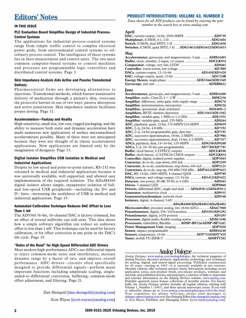
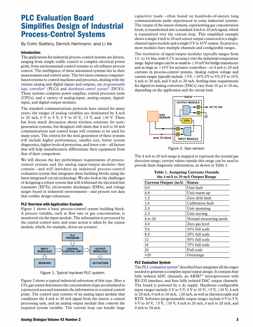
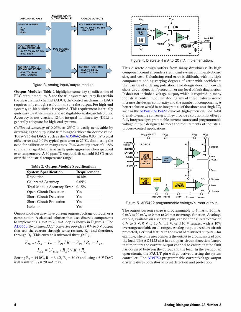
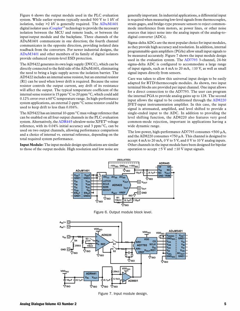
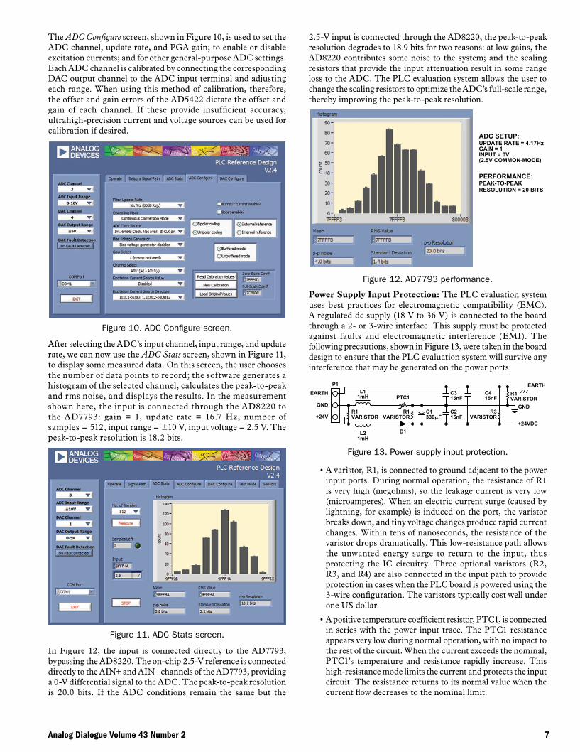
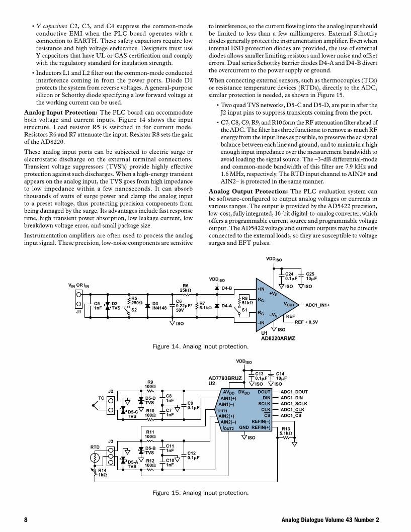
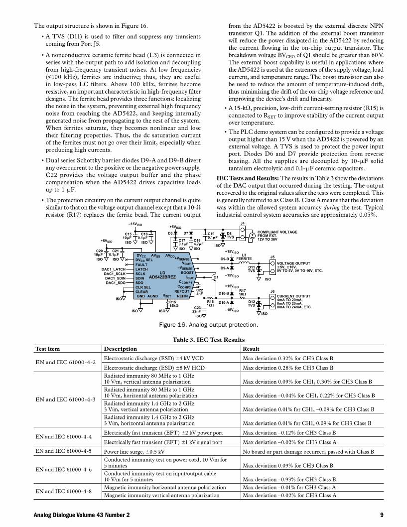
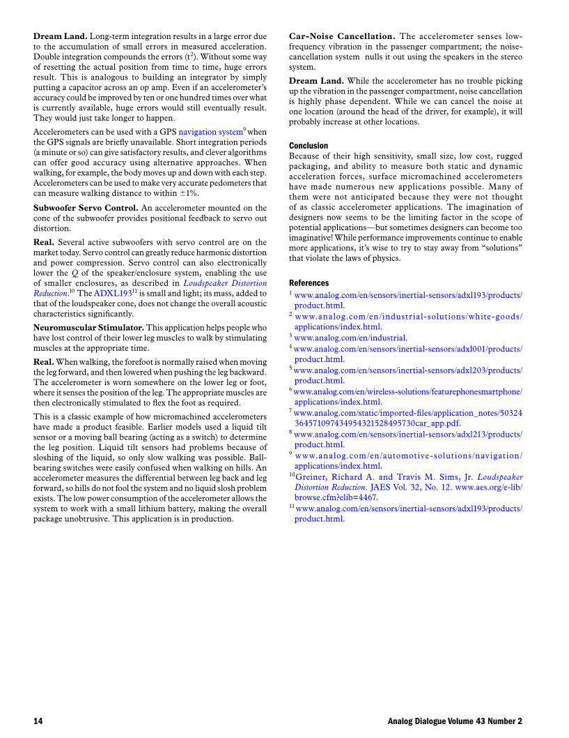
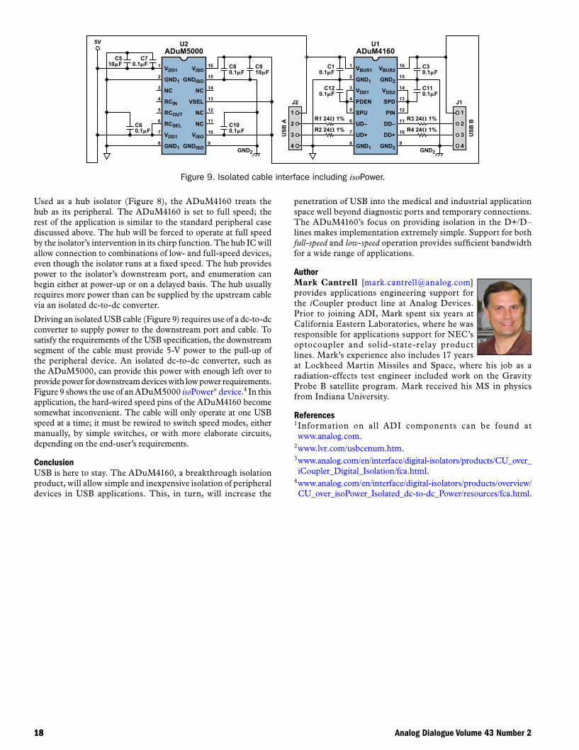
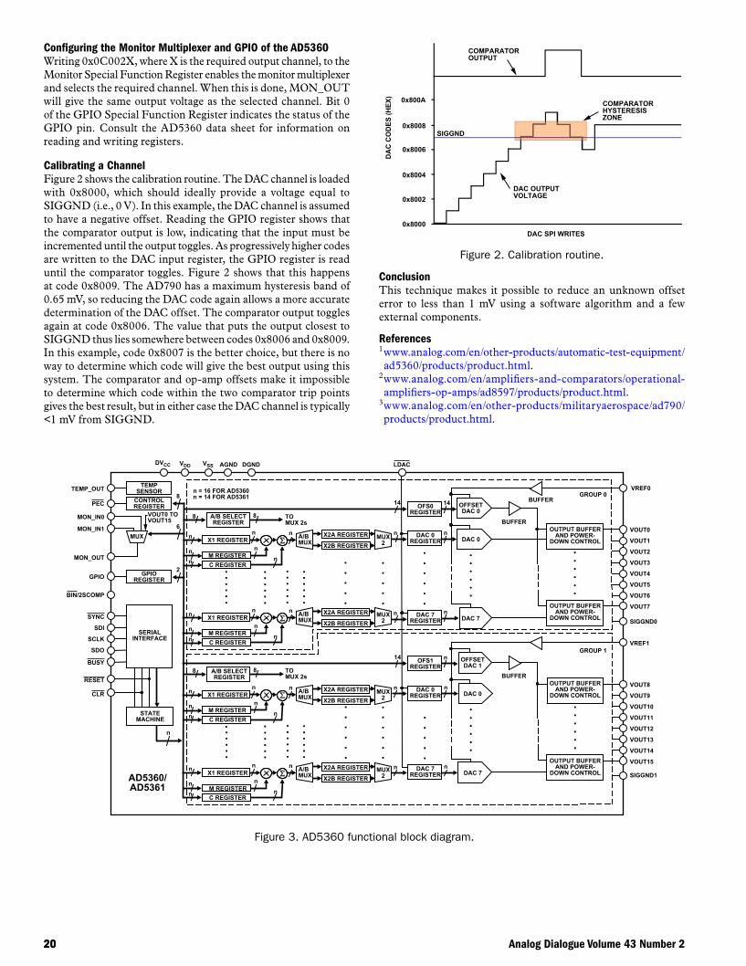
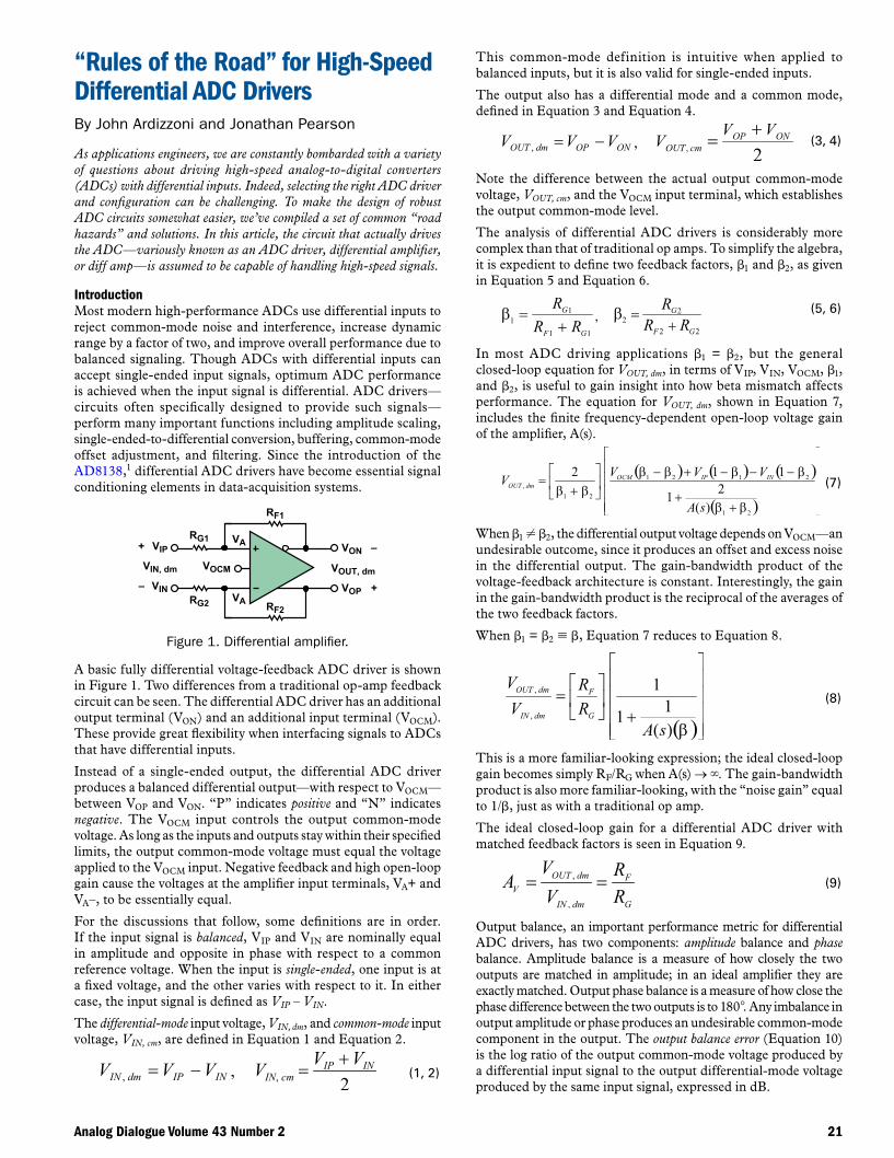
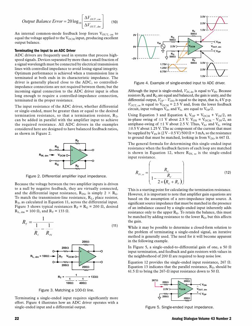
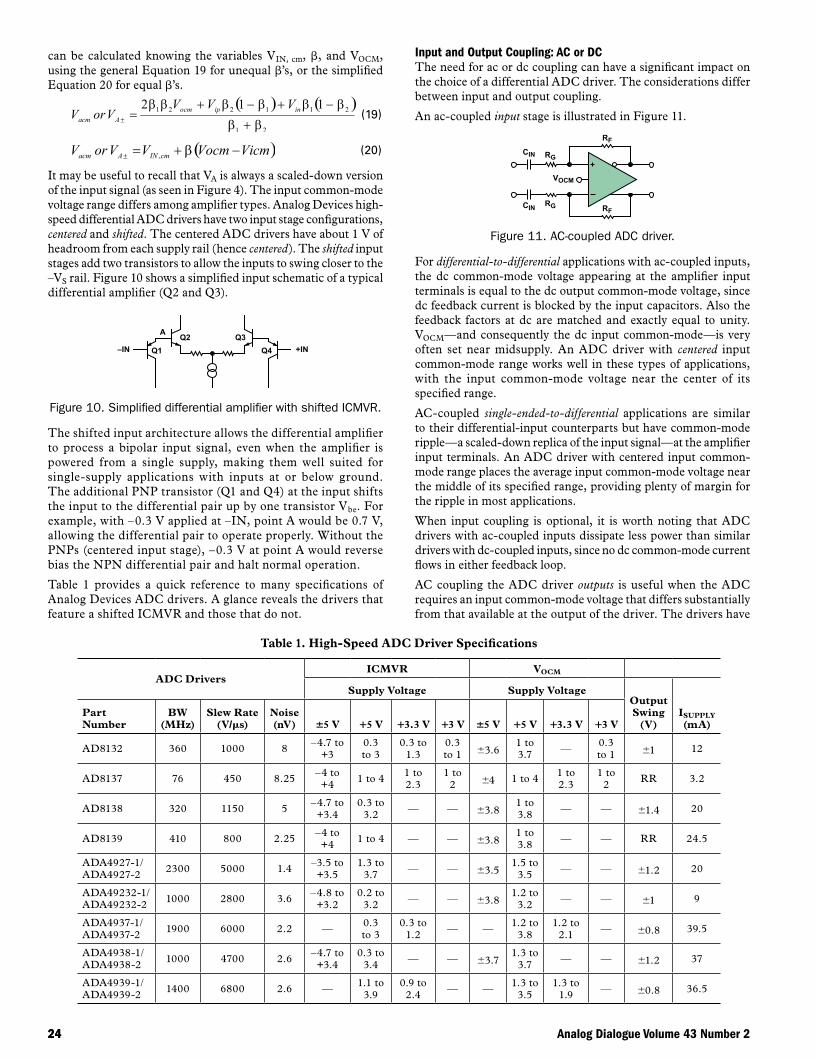