infineon its4090q-ep-d-data sheet
TRANSCRIPT

Data Sheet 1 Rev. 1.0www.infineon.com/industrial-profet 2018-06-14
Industrial PROFET™ITS4090Q-EP-D 90 mΩ Quad Channel Smart High-Side Power Swi tch
1 Overview
Features• Quad channel Smart High-Side Power Switch with integrated protection
and diagnosis• Maximum RDS(ON) 90 mΩ per channel at Tj = 25°C• Nominal output current capability up to 750 mA• Low and accurate current limitation: 1.5 A (± 20 %)• Extended supply voltage range up to 45 V• All control inputs 24 V capable and support direct interface to optocouplers• All control inputs 3.3 V and 5 V logic level compatible• 4 kV electrostatic discharge protection (ESD)• Optimized electromagnetic compatibility• Very small, thermally enhanced TSDSO-14 package• Device robustness validated by extended qualification according to JEDEC standard “JESD47J”• Green product (RoHS compliant)
Potential applications• Digital output modules (PLC applications, factory automation)• Industrial peripheral switches and power distribution• Switching resistive, inductive and capacitive loads in harsh industrial environments• Replacement for electromechanical relays, fuses and discrete circuits• Most suitable for loads that require a precise current limit
Product validationQualified for industrial applications according to the relevant tests of JEDEC JESD47J.

Data Sheet 2 Rev. 1.0 2018-06-14
ITS4090Q-EP-D90 mΩ Quad Channel Smart High-Side Power Switch
Overview
DescriptionThe ITS4090Q-EP-D is a 90 mΩ Quad Channel Smart High-Side Power Switch providing integrated protectionfunctions and a diagnosis feedback. With four channels capable of currents of more than 500 mA each, verylow typical RDS(ON) values of 140 mΩ at Tj = 125°C and the small PG-TSDSO-14 exposed pad package itcombines high flexibility with minimum space requirements. The exposed pad of the thermally enhanced PG-TSDSO-14 package allows a very efficient heat transfer from the device to inner layers of the PCB by means ofthermal vias. The power transistors are built by N-channel vertical power MOSFETs (DMOS) with charge pump.The ITS4090Q-EP-D is specifically designed to switch resistive, inductive or capacitive loads in harsh industrialenvironments. The ITS4090Q-EP-D is equipped with essential protection features that make it extremelyrobust. Diagnostic information can be read out via the STATUS output (ST). The four channel device can becontrolled with four separate input pins. Due to their high voltage capability the input pins can be directlyinterfaced to optocouplers without additional external components.
Diagnostic Functions• Short circuit to ground (overload) indication• Overtemperature switch off indication• Stable diagnostic signal during short circuit and overtemperature shutdown• Intelligent channel fault detection system
Protection Functions• Stable behavior during undervoltage• Overtemperature protection with restart after cooling down phase• Overload- and short circuit protection• Reverse polarity / inverse current protection with external components• Overvoltage protection with external components• Loss of ground protection
The qualification of this product is based on JEDEC JESD47J and may reference existing qualification resultsof similar products. Such referring is justified by the structural similarity of the products. The product is notqualified and manufactured according to the requirements of Infineon Technologies with regard toautomotive and/or transportation applications. Infineon Technologies administrates a comprehensivequality management system according to the latest version of the ISO9001 and IATF 16949.The most updated certificates of the ISO9001 and IATF 16949 are available atwww.infineon.com/cms/en/product/technology/quality/
Type Package MarkingITS4090Q-EP-D PG-TSDSO-14 ITS4090Q

Data Sheet 3 Rev. 1.0 2018-06-14
ITS4090Q-EP-D90 mΩ Quad Channel Smart High-Side Power Switch
1 Overview . . . . . . . . . . . . . . . . . . . . . . . . . . . . . . . . . . . . . . . . . . . . . . . . . . . . . . . . . . . . . . . . . . . . . . . . 1
Features . . . . . . . . . . . . . . . . . . . . . . . . . . . . . . . . . . . . . . . . . . . . . . . . . . . . . . . . . . . . . . . . . . . . . . . . 1
Potential applications . . . . . . . . . . . . . . . . . . . . . . . . . . . . . . . . . . . . . . . . . . . . . . . . . . . . . . . . . . . . . 1
Product validation . . . . . . . . . . . . . . . . . . . . . . . . . . . . . . . . . . . . . . . . . . . . . . . . . . . . . . . . . . . . . . . . 1
Description . . . . . . . . . . . . . . . . . . . . . . . . . . . . . . . . . . . . . . . . . . . . . . . . . . . . . . . . . . . . . . . . . . . . . . 2
Table of Contents . . . . . . . . . . . . . . . . . . . . . . . . . . . . . . . . . . . . . . . . . . . . . . . . . . . . . . . . . . . . . . . . . 3
2 Block Diagram . . . . . . . . . . . . . . . . . . . . . . . . . . . . . . . . . . . . . . . . . . . . . . . . . . . . . . . . . . . . . . . . . . . 5
3 Pin Configuration . . . . . . . . . . . . . . . . . . . . . . . . . . . . . . . . . . . . . . . . . . . . . . . . . . . . . . . . . . . . . . . . . 63.1 Pin Assignment PG-TSDSO-14 . . . . . . . . . . . . . . . . . . . . . . . . . . . . . . . . . . . . . . . . . . . . . . . . . . . . . . . . . . . . . . 63.2 Pin Definitions and Functions PG-TSDSO-14 . . . . . . . . . . . . . . . . . . . . . . . . . . . . . . . . . . . . . . . . . . . . . . . . . 63.3 Voltage and Current Definitions . . . . . . . . . . . . . . . . . . . . . . . . . . . . . . . . . . . . . . . . . . . . . . . . . . . . . . . . . . . . 7
4 General Product Characteristics . . . . . . . . . . . . . . . . . . . . . . . . . . . . . . . . . . . . . . . . . . . . . . . . . . . . 84.1 Absolute Maximum Ratings . . . . . . . . . . . . . . . . . . . . . . . . . . . . . . . . . . . . . . . . . . . . . . . . . . . . . . . . . . . . . . . . 84.2 Functional Range . . . . . . . . . . . . . . . . . . . . . . . . . . . . . . . . . . . . . . . . . . . . . . . . . . . . . . . . . . . . . . . . . . . . . . . . 104.3 Typical Performance Characteristics Operating Current . . . . . . . . . . . . . . . . . . . . . . . . . . . . . . . . . . . . . 114.4 Thermal Resistance . . . . . . . . . . . . . . . . . . . . . . . . . . . . . . . . . . . . . . . . . . . . . . . . . . . . . . . . . . . . . . . . . . . . . . 12
5 Power Stage . . . . . . . . . . . . . . . . . . . . . . . . . . . . . . . . . . . . . . . . . . . . . . . . . . . . . . . . . . . . . . . . . . . . 145.1 Output ON-state Resistance . . . . . . . . . . . . . . . . . . . . . . . . . . . . . . . . . . . . . . . . . . . . . . . . . . . . . . . . . . . . . . 145.2 Turn ON/OFF Characteristics with Resistive Load . . . . . . . . . . . . . . . . . . . . . . . . . . . . . . . . . . . . . . . . . . . 145.3 Inductive Load . . . . . . . . . . . . . . . . . . . . . . . . . . . . . . . . . . . . . . . . . . . . . . . . . . . . . . . . . . . . . . . . . . . . . . . . . . 155.3.1 Output Clamping . . . . . . . . . . . . . . . . . . . . . . . . . . . . . . . . . . . . . . . . . . . . . . . . . . . . . . . . . . . . . . . . . . . . . . 155.3.2 Maximum Load Inductance . . . . . . . . . . . . . . . . . . . . . . . . . . . . . . . . . . . . . . . . . . . . . . . . . . . . . . . . . . . . . 165.4 Inverse Current Capability . . . . . . . . . . . . . . . . . . . . . . . . . . . . . . . . . . . . . . . . . . . . . . . . . . . . . . . . . . . . . . . . 165.5 Electrical Characteristics: Power Stage . . . . . . . . . . . . . . . . . . . . . . . . . . . . . . . . . . . . . . . . . . . . . . . . . . . . 185.6 Typical Performance Characteristics Power Stage . . . . . . . . . . . . . . . . . . . . . . . . . . . . . . . . . . . . . . . . . . 20
6 Protection Functions . . . . . . . . . . . . . . . . . . . . . . . . . . . . . . . . . . . . . . . . . . . . . . . . . . . . . . . . . . . . . 236.1 Loss of Ground Protection . . . . . . . . . . . . . . . . . . . . . . . . . . . . . . . . . . . . . . . . . . . . . . . . . . . . . . . . . . . . . . . . 236.2 Undervoltage Protection . . . . . . . . . . . . . . . . . . . . . . . . . . . . . . . . . . . . . . . . . . . . . . . . . . . . . . . . . . . . . . . . . 246.2.1 Overvoltage Protection . . . . . . . . . . . . . . . . . . . . . . . . . . . . . . . . . . . . . . . . . . . . . . . . . . . . . . . . . . . . . . . . . 246.3 Reverse Polarity Protection . . . . . . . . . . . . . . . . . . . . . . . . . . . . . . . . . . . . . . . . . . . . . . . . . . . . . . . . . . . . . . . 266.4 Overload Protection . . . . . . . . . . . . . . . . . . . . . . . . . . . . . . . . . . . . . . . . . . . . . . . . . . . . . . . . . . . . . . . . . . . . . 276.4.1 Current Limitation . . . . . . . . . . . . . . . . . . . . . . . . . . . . . . . . . . . . . . . . . . . . . . . . . . . . . . . . . . . . . . . . . . . . . 276.4.2 Temperature Limitation in the Power DMOS . . . . . . . . . . . . . . . . . . . . . . . . . . . . . . . . . . . . . . . . . . . . . . 286.5 Electrical Characteristics: Protection Functions . . . . . . . . . . . . . . . . . . . . . . . . . . . . . . . . . . . . . . . . . . . . . 286.6 Typical Performance Characteristics Protection Functions . . . . . . . . . . . . . . . . . . . . . . . . . . . . . . . . . . . 29
7 Diagnostic Functions . . . . . . . . . . . . . . . . . . . . . . . . . . . . . . . . . . . . . . . . . . . . . . . . . . . . . . . . . . . . . 307.1 Electrical Characteristics: Diagnostic Functions . . . . . . . . . . . . . . . . . . . . . . . . . . . . . . . . . . . . . . . . . . . . . 307.2 Channel Fault Detection . . . . . . . . . . . . . . . . . . . . . . . . . . . . . . . . . . . . . . . . . . . . . . . . . . . . . . . . . . . . . . . . . . 317.3 Typical Performance Characteristics Diagnostic Functions . . . . . . . . . . . . . . . . . . . . . . . . . . . . . . . . . . . 33
8 Input Pins . . . . . . . . . . . . . . . . . . . . . . . . . . . . . . . . . . . . . . . . . . . . . . . . . . . . . . . . . . . . . . . . . . . . . . 348.1 Input Circuitry . . . . . . . . . . . . . . . . . . . . . . . . . . . . . . . . . . . . . . . . . . . . . . . . . . . . . . . . . . . . . . . . . . . . . . . . . . . 348.2 Input Pin Voltage . . . . . . . . . . . . . . . . . . . . . . . . . . . . . . . . . . . . . . . . . . . . . . . . . . . . . . . . . . . . . . . . . . . . . . . . 34
Table of Contents
Data Sheet 4 Rev. 1.0 2018-06-14
ITS4090Q-EP-D90 mΩ Quad Channel Smart High-Side Power Switch
8.3 Electrical Characteristics: Input Pins . . . . . . . . . . . . . . . . . . . . . . . . . . . . . . . . . . . . . . . . . . . . . . . . . . . . . . . 358.4 Typical Performance Characteristics Input Pins . . . . . . . . . . . . . . . . . . . . . . . . . . . . . . . . . . . . . . . . . . . . . 36
9 Application Information . . . . . . . . . . . . . . . . . . . . . . . . . . . . . . . . . . . . . . . . . . . . . . . . . . . . . . . . . . 379.1 Application Diagram . . . . . . . . . . . . . . . . . . . . . . . . . . . . . . . . . . . . . . . . . . . . . . . . . . . . . . . . . . . . . . . . . . . . . 379.2 Thermal Considerations . . . . . . . . . . . . . . . . . . . . . . . . . . . . . . . . . . . . . . . . . . . . . . . . . . . . . . . . . . . . . . . . . . 38
10 Package Outlines . . . . . . . . . . . . . . . . . . . . . . . . . . . . . . . . . . . . . . . . . . . . . . . . . . . . . . . . . . . . . . . . 40
11 Revision History . . . . . . . . . . . . . . . . . . . . . . . . . . . . . . . . . . . . . . . . . . . . . . . . . . . . . . . . . . . . . . . . . 41
Data Sheet 5 Rev. 1.0 2018-06-14
ITS4090Q-EP-D90 mΩ Quad Channel Smart High-Side Power Switch
Block Diagram
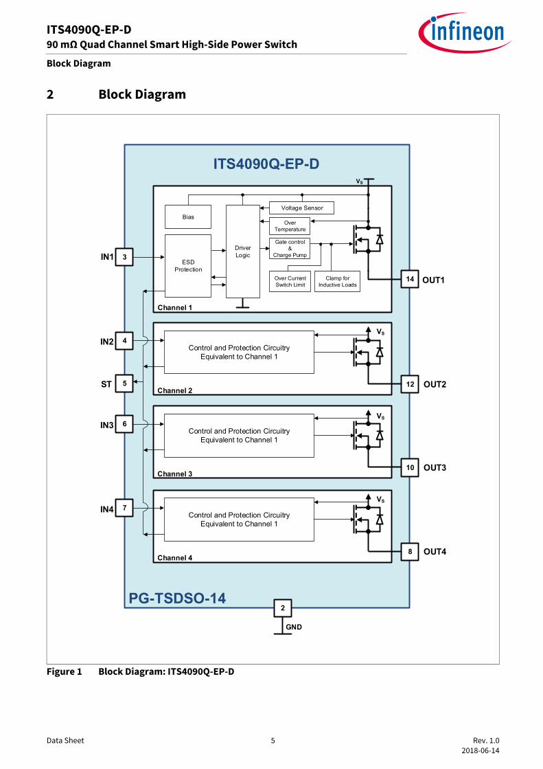
2 Block Diagram
Figure 1 Block Diagram: ITS4090Q-EP-D
IN1
ST
IN2
IN3
IN4
PG-TSDSO-14
ITS4090Q-EP-D
3
14
2
OUT1
5
Bias
ESDProtection
DriverLogic
OverTemperature
Voltage Sensor
Clamp forInductive Loads
Gate control&
Charge Pump
Over Current Switch Limit
VS
12 OUT2
4Control and Protection Circuitry
Equivalent to Channel 1
Channel 1
Channel 2
10 OUT3
6Control and Protection Circuitry
Equivalent to Channel 1
Channel 3
8 OUT4
7Control and Protection Circuitry
Equivalent to Channel 1
Channel 4
VS
VS
VS
GND
Data Sheet 6 Rev. 1.0 2018-06-14
ITS4090Q-EP-D90 mΩ Quad Channel Smart High-Side Power Switch
Pin Configuration
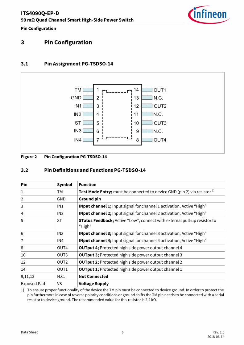
3 Pin Configuration
3.1 Pin Assignment PG-TSDSO-14
Figure 2 Pin Configuration PG-TSDSO-14
3.2 Pin Definitions and Functions PG-TSDSO-14
Pin Symbol Function1 TM Test Mode Entry; must be connected to device GND (pin 2) via resistor 1)
1) To ensure proper functionality of the device the TM pin must be connected to device ground. In order to protect the pin furthermore in case of reverse polarity conditions or ground shifts the TM pin needs to be connected with a serial resistor to device ground. The recommended value for this resistor is 2.2 kΩ.
2 GND Ground pin3 IN1 INput channel 1; Input signal for channel 1 activation, Active “High”
4 IN2 INput channel 2; Input signal for channel 2 activation, Active “High”
5 ST STatus Feedback; Active “Low”, connect with external pull-up resistor to “High”
6 IN3 INput channel 3; Input signal for channel 3 activation, Active “High”
7 IN4 INput channel 4; Input signal for channel 4 activation, Active “High”
8 OUT4 OUTput 4; Protected high side power output channel 4
10 OUT3 OUTput 3; Protected high side power output channel 3
12 OUT2 OUTput 2; Protected high side power output channel 2
14 OUT1 OUTput 1; Protected high side power output channel 1
9,11,13 N.C. Not ConnectedExposed Pad VS Voltage Supply
OUT1
OUT4
N.C.
OUT3
N.C.
OUT2
N.C.
TM
IN4
ST
IN1
IN2
GND
1
2
3
4
5
6
7
14
9
10
11
12
13
8
IN3

Data Sheet 7 Rev. 1.0 2018-06-14
ITS4090Q-EP-D90 mΩ Quad Channel Smart High-Side Power Switch
Pin Configuration
3.3 Voltage and Current DefinitionsFigure 3 shows all terms used in this data sheet, with associated convention for positive values.
Figure 3 Voltage and Current Definitions
IN1
IN2
IN3
IN4
ST
VS
GND
OUT1
OUT2
OUT 3
OUT 4
ITS4090Q-EP-DVS
VIN
1
VIN
2
VIN
3
VIN
4
VS
T
IIN1
IIN2
IIN3
IIN4
IST
IS
IOUT1
IOUT2
IOUT3
IOUT4
VD
S1
VD
S2
VD
S3
VD
S4
VO
UT1
VO
UT2
VO
UT3
VO
UT4
IGND

Data Sheet 8 Rev. 1.0 2018-06-14
ITS4090Q-EP-D90 mΩ Quad Channel Smart High-Side Power Switch
General Product Characteristics
4 General Product Characteristics
4.1 Absolute Maximum Ratings
Table 1 Absolute Maximum Ratings 1)
Tj = -40°C to 150°C, positive current flowing into pin; (unless otherwise specified)
Parameter Symbol Values Unit Note or Test Condition NumberMin. Typ. Max.
Supply VoltagesSupply voltage VS -0.3 – 45 V – P_4.1.1Reverse polarity voltage -VS(REV) 0 – 28 V 2) t < 2 min
TA = 25°C RL ≥ 25 Ω ZGND = 150 Ω Power Resistor
P_4.1.3
Supply voltage for short circuit protection
VS(SC) 0 – 36 V – P_4.1.4
Input PinsVoltage at INPUT pins VIN -0.3 – 45 V VS > VIN P_4.1.5Current through INPUT pins IIN -2 – 2 mA – P_4.1.6STATUS PinVoltage at ST pin VST -0.3 – 45 V VS > VST P_4.1.7Current through ST pin IST -2 – 2 mA – P_4.1.8Power StagePower dissipation (DC) PTOT – – 1.8 W 3) TA = 85°C
Tj < 150°CP_4.1.10
Maximum energy dissipation Single pulse (one channel)
EAS – – 410 mJ IL = 0.5 A Tj = 150°C VS = 28 V
P_4.1.11
Voltage at power transistor VDS – – 65 V – P_4.1.12CurrentsCurrent through ground pin I GND -20 – 20 mA – P_4.1.13Temporary reverse current through ground pin to VS
I GND -200 – – mA t < 2 min P_4.1.21
TemperaturesJunction temperature Tj -40 – 150 °C – P_4.1.14Storage temperature TSTG -55 – 150 °C – P_4.1.15ESD SusceptibilityESD susceptibility (all pins) VESD_HBM -2 – 2 kV HBM4) P_4.1.16ESD susceptibility OUT Pin vs. GND and VS connected
VESD_HBM -4 – 4 kV HBM4) P_4.1.17

Data Sheet 9 Rev. 1.0 2018-06-14
ITS4090Q-EP-D90 mΩ Quad Channel Smart High-Side Power Switch
General Product Characteristics
Notes1. Stresses above the ones listed here may cause permanent damage to the device. Exposure to absolute
maximum rating conditions for extended periods may affect device reliability.2. Integrated protection functions are designed to prevent IC destruction under fault conditions described in
the data sheet. Fault conditions are considered as “outside” normal operating range. Protection functions are not designed for continuous repetitive operation.
ESD susceptibility VESD_CDM -500 – 500 V CDM5) P_4.1.18ESD susceptibility pin(corner pins)
VESD_CDM -750 – 750 V CDM5) P_4.1.19
1) Not subject to production test; specified by design.2) Reverse polarity protection can only be achieved in combination with external components: to limit the current
through the GND-path a 150 Ω power resistor needs to be placed between GND-pin and ground. An alternative solution is to use a reverse current diode in the GND-path to realize reverse polarity protection. In this case placing a resistor in the range of ≥ 27 Ω in series to the diode is recommended to improve at the same time the overvoltage capability in case of overvoltage pulses on VS.
3) This parameter serves as reference for the thermal budget: it illustrates the power dissipation that can be handled by the device in an application under the given boundary conditions before exceeding the maximum rating of Tj when assuming a RthJA value for a thermally well dimensioned PCB connection like given in the JEDEC case P_4.3.3 in Chapter 4.4. As RthJA depends strongly on the applied PCB and layout of any individual application the actual achievable values of PTOT can either be lower or higher depending on the given application.
4) ESD susceptibility, HBM according to ANSI/ESDA/JEDEC JS-001(1.5 kΩ, 100 pF).5) ESD susceptibility, Charged Device Model “CDM” JEDEC JESD22-C101.
Table 1 Absolute Maximum Ratings 1) (cont’d)Tj = -40°C to 150°C, positive current flowing into pin; (unless otherwise specified)
Parameter Symbol Values Unit Note or Test Condition NumberMin. Typ. Max.
Data Sheet 10 Rev. 1.0 2018-06-14
ITS4090Q-EP-D90 mΩ Quad Channel Smart High-Side Power Switch
General Product Characteristics
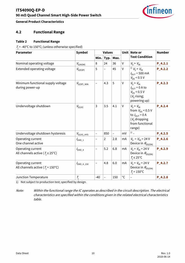
4.2 Functional Range
Note: Within the functional range the IC operates as described in the circuit description. The electrical characteristics are specified within the conditions given in the related electrical characteristics table.
Table 2 Functional RangeTj = -40°C to 150°C; (unless otherwise specified)
Parameter Symbol Values Unit Note or Test Condition
NumberMin. Typ. Max.
Nominal operating voltage VS(NOM) 8 24 36 V VS > VIN P_4.2.1Extended operating voltage VS(EOP) 5 – 45 V 1) VS > VIN
IOUT = 500 mA VDS < 0.5 V
P_4.2.2
Minimum functional supply voltage during power-up
VS(OP)_MIN – 4.3 5 V VS > VIN IOUT = 0 A to VDS < 0.5 V (VS rising; powering up)
P_4.2.3
Undervoltage shutdown VS(UV) 3 3.5 4.1 V VS > VIN from VDS < 0.5 V to IOUT = 0 A (VS dropping from functional range)
P_4.2.4
Undervoltage shutdown hysteresis VS(UV)_HYS – 850 – mV 1) –
1) Not subject to production test; specified by design.
P_4.2.5Operating current One channel active
IGND_1 – 2 2.8 mA VS = VIN = 24 V Device in RDS(ON)
P_4.2.6
Operating current All channels active (Tj ≤ 25°C)
IGND_4 – 5.2 6.8 mA VS = VIN = 24 V Device in RDS(ON)Tj ≤ 25°C
P_4.2.9
Operating current All channels active (Tj = 150°C)
IGND_4_150 – 4.8 6.0 mA VS = VIN = 24 V Device in RDS(ON)Tj = 150°C
P_4.2.7
Junction Temperature Tj -40 – 150 °C – P_4.2.8

Data Sheet 11 Rev. 1.0 2018-06-14
ITS4090Q-EP-D90 mΩ Quad Channel Smart High-Side Power Switch
General Product Characteristics
4.3 Typical Performance Characteristics Operating Current
Typical Performance Characteristics
Operating Current IGND versusJunction Temperature Tj
Operating Current IGND versusSupply VoltageVS
−50 0 50 100 1500
1
2
3
4
5
6
7
Tj [°C]
I GN
D [m
A]
VS = 24 V 1 channel active 2 channels active 3 channels active 4 channels active
0 10 20 30 400
1
2
3
4
5
6
7
VS [V]
I GN
D [m
A]
Tj = 25 °C
1 channel active 2 channels active 3 channels active 4 channels active
Data Sheet 12 Rev. 1.0 2018-06-14
ITS4090Q-EP-D90 mΩ Quad Channel Smart High-Side Power Switch
General Product Characteristics
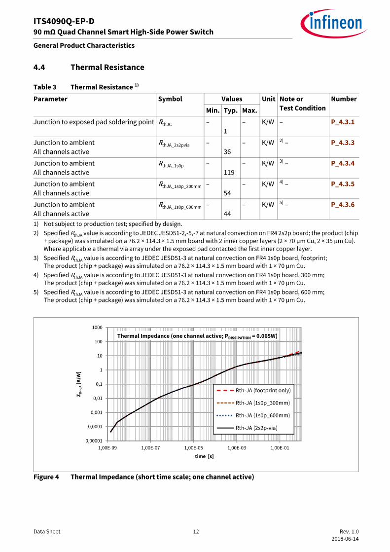
4.4 Thermal Resistance
Figure 4 Thermal Impedance (short time scale; one channel active)
Table 3 Thermal Resistance 1)
1) Not subject to production test; specified by design.
Parameter Symbol Values Unit Note or Test Condition
NumberMin. Typ. Max.
Junction to exposed pad soldering point RthJC –1
– K/W – P_4.3.1
Junction to ambient All channels active
RthJA_2s2pvia –36
– K/W 2) –
2) Specified RthJA value is according to JEDEC JESD51-2,-5,-7 at natural convection on FR4 2s2p board; the product (chip + package) was simulated on a 76.2 × 114.3 × 1.5 mm board with 2 inner copper layers (2 × 70 µm Cu, 2 × 35 µm Cu). Where applicable a thermal via array under the exposed pad contacted the first inner copper layer.
P_4.3.3
Junction to ambient All channels active
RthJA_1s0p –119
– K/W 3) –
3) Specified RthJA value is according to JEDEC JESD51-3 at natural convection on FR4 1s0p board, footprint; The product (chip + package) was simulated on a 76.2 × 114.3 × 1.5 mm board with 1 × 70 µm Cu.
P_4.3.4
Junction to ambient All channels active
RthJA_1s0p_300mm –54
– K/W 4) –
4) Specified RthJA value is according to JEDEC JESD51-3 at natural convection on FR4 1s0p board, 300 mm; The product (chip + package) was simulated on a 76.2 × 114.3 × 1.5 mm board with 1 × 70 µm Cu.
P_4.3.5
Junction to ambient All channels active
RthJA_1s0p_600mm –44
– K/W 5) –
5) Specified RthJA value is according to JEDEC JESD51-3 at natural convection on FR4 1s0p board, 600 mm; The product (chip + package) was simulated on a 76.2 × 114.3 × 1.5 mm board with 1 × 70 µm Cu.
P_4.3.6
0,00001
0,0001
0,001
0,01
0,1
1
10
100
1000
1,00E-09 1,00E-07 1,00E-05 1,00E-03 1,00E-01
Z tH-J
A[K
/W]
time [s]
Thermal Impedance (one channel active; PDISSIPATION = 0.065W)
Rth-JA (footprint only)
Rth-JA (1s0p_300mm)
Rth-JA (1s0p_600mm)
Rth-JA (2s2p-via)

Data Sheet 13 Rev. 1.0 2018-06-14
ITS4090Q-EP-D90 mΩ Quad Channel Smart High-Side Power Switch
General Product Characteristics
Figure 5 Thermal Impedance (long time scale; one channel active)
0
20
40
60
80
100
120
140
1,00E-05 1,00E-03 1,00E-01 1,00E+01 1,00E+03
Z tH-J
A[K
/W]
time [s]
Thermal Impedance (one channel active; PDISSIPATION = 0.065W)
Rth-JA (footprint only)
Rth-JA (1s0p_300mm)
Rth-JA (1s0p_600mm)
Rth-JA (2s2p-via)

Data Sheet 14 Rev. 1.0 2018-06-14
ITS4090Q-EP-D90 mΩ Quad Channel Smart High-Side Power Switch
Power Stage
5 Power StageThe power stages are built using an N-channel vertical power MOSFET (DMOS) with charge pump.
5.1 Output ON-state ResistanceThe ON-state resistance RDS(ON) of the power stage depends on supply voltage as well as on junctiontemperature Tj. Figure 6 shows the influence of temperature on the typical ON-state resistance. The behaviorof the power stage in reverse polarity condition is described in Chapter 6.3.
Figure 6 Typical ON-state Resistance
5.2 Turn ON/OFF Characteristics with Resistive LoadA “High” signal at the input pin (see Chapter 8) causes the power DMOS to switch ON with a dedicated slope,which is optimized in terms of EMC emission.Figure 7 shows the typical timing when switching a resistive load.
Figure 7 Switching a Resistive Load Timing
−50 0 50 100 1500
20
40
60
80
100
120
140
160
180
Tj [°C]
RD
SO
N [m
Ω ]
IN
t
VOUT
tON
tON_delay tOFF
90% VS
10% VS
VIN_H
VIN_L
t
Switching times.vsd
tOFF_delay
30% VS
70% VS
dV/dt ON dV/dt OFF
Data Sheet 15 Rev. 1.0 2018-06-14
ITS4090Q-EP-D90 mΩ Quad Channel Smart High-Side Power Switch
Power Stage
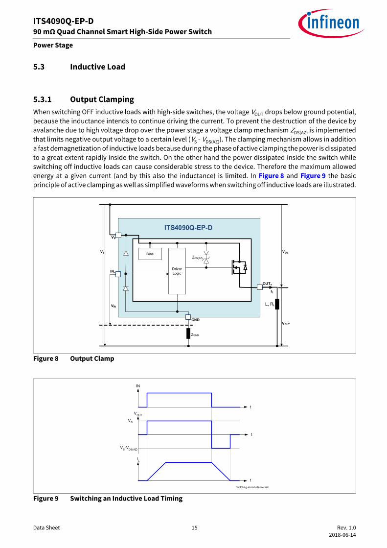
5.3 Inductive Load
5.3.1 Output ClampingWhen switching OFF inductive loads with high-side switches, the voltage VOUT drops below ground potential,because the inductance intends to continue driving the current. To prevent the destruction of the device byavalanche due to high voltage drop over the power stage a voltage clamp mechanism ZDS(AZ) is implementedthat limits negative output voltage to a certain level (VS - VDS(AZ)). The clamping mechanism allows in additiona fast demagnetization of inductive loads because during the phase of active clamping the power is dissipatedto a great extent rapidly inside the switch. On the other hand the power dissipated inside the switch whileswitching off inductive loads can cause considerable stress to the device. Therefore the maximum allowedenergy at a given current (and by this also the inductance) is limited. In Figure 8 and Figure 9 the basicprinciple of active clamping as well as simplified waveforms when switching off inductive loads are illustrated.
Figure 8 Output Clamp
Figure 9 Switching an Inductive Load Timing
ITS4090Q-EP-D
OUTx
INx
VS
DriverLogic
GND
BiasZDS(AZ)
VS
VÎN
IL
L, RL
ZGND
VDS
VOUT
IN
VOUT
IL
VS
VS-VDS(AZ)
t
t
t
Switching an inductance.vsd

Data Sheet 16 Rev. 1.0 2018-06-14
ITS4090Q-EP-D90 mΩ Quad Channel Smart High-Side Power Switch
Power Stage
5.3.2 Maximum Load InductanceDuring demagnetization of inductive loads, the following energy must be dissipated by the ITS4090Q-EP-D.This energy can be calculated by help of the following equation:
(5.1)
Following equation gets simplified under the assumption of RL = 0 Ω:
(5.2)
The energy, which may be converted into heat, is limited by the thermal design of the component. SeeFigure 10 for the maximum allowed energy dissipation as a function of the load current for a singular pulseevent on one channel.
Figure 10 Maximum Energy Dissipation Single Pulse for a Single Channel (Tj = 150°C, VS = 28 V)
5.4 Inverse Current CapabilityIn case of inverse current, meaning a voltage VINV at the OUTput higher than the supply voltage VS, a currentIINV will flow from output to VS pin via the body diode of the power transistor (please refer to Figure 11).Channels that are active (ON-state) by the time when the inverse current condition appears will remain activeand their output stage will follow the state of the corresponding IN pin, which means that the channel can beswitched off during inverse current condition. Channels that are inactive (OFF-state) by the time when theinverse current condition appears will remain inactive regardless of the state of the corresponding IN pin. Ifduring an inverse current condition the IN-pin of a channel is set from “Low” to “High” in order to activate thechannel, the output stage of the channel is kept OFF until the inverse current disappears. For all cases thecurrent IINV should not be higher than IL(INV). Please note that during inverse current condition the protectionfunctions of concerned channels are not available.
E VDS AZ( )LRL------×
VS VDS AZ( )–
RL-------------------------------- 1 RL IL×
VS VDS AZ( )–--------------------------------–⎝ ⎠
⎛ ⎞ln IL+××=
E 12--- L I2 1 VS
VS VDS AZ( )–--------------------------------–⎝ ⎠
⎛ ⎞×××=
0.5 0.6 0.7 0.8 0.9 1 1.1 1.2 1.3 1.4 1.50
50
100
150
200
250
300
350
400
450
ILoad [A]
EA
S [m
J]

Data Sheet 17 Rev. 1.0 2018-06-14
ITS4090Q-EP-D90 mΩ Quad Channel Smart High-Side Power Switch
Power Stage
Figure 11 Inverse Current Circuitry
Figure 12 Inverse Current event: channel in OFF-state (channel remains off for duration of inverse current event)
VS
ITS4090Q-EP-D
OUTx
INx
Device Logic
Gate Driver
GND
Bias
ZGND
Inv.Comp
IL(INV)
VINV
IL(INV)
VIN
t
t
t
ChannelState
„ON“
„OFF“
„OFF“ „ON“
Inverse Current Event

Data Sheet 18 Rev. 1.0 2018-06-14
ITS4090Q-EP-D90 mΩ Quad Channel Smart High-Side Power Switch
Power Stage
Figure 13 Inverse Current event: channel in ON-state (output not influenced but can be switched off)
5.5 Electrical Characteristics: Power Stage
Table 4 Electrical Characteristics: Power StageVS = 8 V to 36 V, Tj = -40°C to 150°C (unless otherwise specified). Typical values are given at VS = 24 V, Tj = 25°C
Parameter Symbol Values Unit Note or Test Condition
NumberMin. Typ. Max.
ON-state resistance per channel (Tj = 25°C)
RDS(ON) – – 90 mΩ ILx = 0.5 A VIN = 4.5 V Tj = 25°C
P_5.5.18
ON-state resistance per channel (Tj = 125°C)
RDS(ON)_125 – 140 – mΩ 2) ILx = 0.5 AVIN = 4.5 VTj = 125°C
P_5.5.19
ON-state resistance per channel (Tj = 150°C)
RDS(ON)_150 – – 180 mΩ ILx= 0.5 A VIN = 4.5 V Tj = 150°C
P_5.5.1
Nominal load current per channel
IL(NOM)1 – – 750 mA 1) 2) Tj < 150°C P_5.5.2
Drain to source clamping voltage VDS(AZ) = [VS - VOUT]
VDS(AZ) 65 70 75 V IDS = 5 mA P_5.5.5
Output leakage current per channel
IL(OFF) – 0.1 0.5 µA 2) VIN floating VOUT = 0 V Tj ≤ 85°C
P_5.5.6
Output leakage current per channel
IL(OFF)_150 – 1 5 µA VIN floating VOUT = 0 V Tj = 150°C
P_5.5.4
Inverse current capability IL(INV) – 2.2 – A 2) 3) VS < VOUTX t < 2 min
P_5.5.7
„ON“
„OFF“
IL(INV)
VIN
ChannelState
t
t
t
„OFF“ „ON“ „OFF“
Inverse Current Event

Data Sheet 19 Rev. 1.0 2018-06-14
ITS4090Q-EP-D90 mΩ Quad Channel Smart High-Side Power Switch
Power Stage
Slew rate (switch on) 30% to 70% of VS
ΔV/ΔtON – 1.75 – V/µs RL = 47 Ω VS = 24 V
P_5.5.8
Slew rate (switch off) 70% to 30% of VS
-ΔV/ΔtOFF – 1.75 – V/µs RL = 47 Ω VS = 24 V
P_5.5.9
Turn-ON time to VOUT = 90% VS tON – 25 75 µs RL = 47 Ω VS = 24 V
P_5.5.11
Turn-OFF time to VOUT = 10% VS
tOFF – 25 75 µs RL = 47 Ω VS = 24 V
P_5.5.12
Turn-ON / OFF matching tOFF - tON
ΔtSW -40 0 40 µs RL = 47 Ω VS = 24 V
P_5.5.13
Turn-ON time to VOUT = 10% VS
tON_delay – 13 45 µs RL = 47 Ω VS = 24 V
P_5.5.14
Turn-OFF time to VOUT = 90% VS
tOFF_delay – 13 45 µs RL = 47 Ω VS = 24 V
P_5.5.15
1) This parameter describes the nominal load capability per channel from an electrical point of view respecting a maximum Tj ≤ 150°C. Please note that depending on the individual thermal design of a real application (and a potentially insufficient thermal budget resulting hereof) additional restrictions for IL(NOM) may occur for pure thermal reasons in order not to exceed the maximum allowed junction temperature Tj = 150°C. The latter needs to be considered especially for cases where all four channels are operating simultaneously under high load conditions and at high ambient temperature TAMB. For further details about potential derating of the nominal load current due to thermal restrictions please refer to “Thermal Considerations” on Page 38.
2) Not subject to production test; specified by design.3) Please note that during inverse current condition the protection features are not operational.
Table 4 Electrical Characteristics: Power Stage (cont’d)VS = 8 V to 36 V, Tj = -40°C to 150°C (unless otherwise specified). Typical values are given at VS = 24 V, Tj = 25°C
Parameter Symbol Values Unit Note or Test Condition
NumberMin. Typ. Max.

Data Sheet 20 Rev. 1.0 2018-06-14
ITS4090Q-EP-D90 mΩ Quad Channel Smart High-Side Power Switch
Power Stage
5.6 Typical Performance Characteristics Power Stage
Typical Performance Characteristics
ON-State Resistance RDSON versusJunction Temperature Tj
Leakage Current per channel IL(OFF) versusJunction Temperature Tj
Output Clamp Voltage VDS(AZ) versusJunction Temperature Tj
−50 0 50 100 1500
20
40
60
80
100
120
140
160
180
Tj [°C]
RD
SO
N [m
Ω ]
VS = 24 V; I Load = 0.5A
−50 0 50 100 1500
0.2
0.4
0.6
0.8
1
1.2
1.4
1.6
1.8
2
Tj [°C]
I L(O
FF
) [uA
]
VS = 24 V
−50 0 50 100 15065
66
67
68
69
70
71
72
73
74
75
Tj [°C]
VD
S(A
Z) [V
]
CH 1 CH 2 CH 3 CH 4

Data Sheet 21 Rev. 1.0 2018-06-14
ITS4090Q-EP-D90 mΩ Quad Channel Smart High-Side Power Switch
Power Stage
Turn-ON time tON to VOUT = 90% versusJunction Temperature Tj
Turn-OFF time tOFF to VOUT = 90% versusJunction Temperature Tj
Turn-ON delay time tON_delay to VOUT = 10% versus Junction Temperature Tj
Turn-OFF time delay tOFF_delay to VOUT = 10% versus Junction Temperature Tj
−50 0 50 100 1500
10
20
30
40
50
60
70
Tj [°C]
t ON [u
s]
VS = 24V I Load = 10mA
I Load = 0.5A
I Load = 0.8A
−50 0 50 100 1500
10
20
30
40
50
60
70
Tj [°C]
t OF
F [u
s]
VS = 24V I Load = 10mA
I Load = 0.5A
I Load = 0.8A
−50 0 50 100 1500
5
10
15
20
25
30
35
40
45
50
Tj [°C]
t ON
_del
ay [u
s]
VS = 24V I Load = 10mA
I Load = 0.5A
I Load = 0.8A
−50 0 50 100 1500
5
10
15
20
25
30
35
40
45
50
Tj [°C]
t OF
F_d
elay
[us]
VS = 24V I Load = 10mA
I Load = 0.5A
I Load = 0.8A

Data Sheet 22 Rev. 1.0 2018-06-14
ITS4090Q-EP-D90 mΩ Quad Channel Smart High-Side Power Switch
Power Stage
Turn-ON time tON to VOUT = 90% versusLoad Current I Load
Turn-OFF time tOFF to VOUT = 90% versus Load Current I Load
Turn-ON delay time tON_delay to VOUT = 10% versus Load Current I Load
Turn-OFF delay time tOFF_delay to VOUT = 10% versus Load Current I Load
0 0.2 0.4 0.6 0.80
10
20
30
40
50
60
70
ILoad [A]
t ON [u
s]
VS = 24 V
Tj = −40 °C
Tj = 25 °C
Tj = 150 °C
0 0.2 0.4 0.6 0.80
10
20
30
40
50
60
70
ILoad [A]
t OF
F [u
s]
VS = 24 V
Tj = −40 °C
Tj = 25 °C
Tj = 150 °C
0 0.2 0.4 0.6 0.80
5
10
15
20
25
30
35
40
45
50
ILoad [A]
t ON
_del
ay [u
s]
VS = 24 V
Tj = −40 °C
Tj = 25 °C
Tj = 150 °C
0 0.2 0.4 0.6 0.80
5
10
15
20
25
30
35
40
45
50
ILoad [A]
t OF
F_d
elay
[us]
VS = 24 V
Tj = −40 °C
Tj = 25 °C
Tj = 150 °C

Data Sheet 23 Rev. 1.0 2018-06-14
ITS4090Q-EP-D90 mΩ Quad Channel Smart High-Side Power Switch
Protection Functions
6 Protection FunctionsThe device provides integrated protection functions. Exposure to absolute maximum rating conditions forextended periods may affect device reliability. Protection functions are designed to prevent the destruction ofthe ITS4090Q-EP-D due to fault conditions described in the data sheet. Please note that fault conditions arenot considered as normal operation conditions and the protection functions are neither designed forcontinuous operation nor for repetitive operation.
6.1 Loss of Ground ProtectionIn case of loss of module ground when the load remains connected to ground, the device protects itself byautomatically turning OFF (when it was previously ON) or remains OFF, regardless of the voltage applied at theinput pins.In an application where the inputs are directly controlled by logic levels < VS (e.g. by a microcontroller withoutgalvanic isolation), it is recommended to use input resistors 1) between the external control circuit(microcontroller) and the ITS4090Q-EP-D to protect also the external control circuit in case of loss of deviceground.In case of loss of module or device ground, a current (IOUT(GND)) can flow out of the DMOS. Figure 14 sketchesthe situation.ZGND is recommended to be a resistor in series to a diode.
Figure 14 Loss of Ground Protection with External Components
1) Recommended value is 10 kΩ
ITS4090Q-EP-D
OUTx
INx
VS
Logic
GND
ZDS(AZ)
IOUT(GND)
ZGND
ZD(AZ)ST
RIN
RST
+-
Data Sheet 24 Rev. 1.0 2018-06-14
ITS4090Q-EP-D90 mΩ Quad Channel Smart High-Side Power Switch
Protection Functions
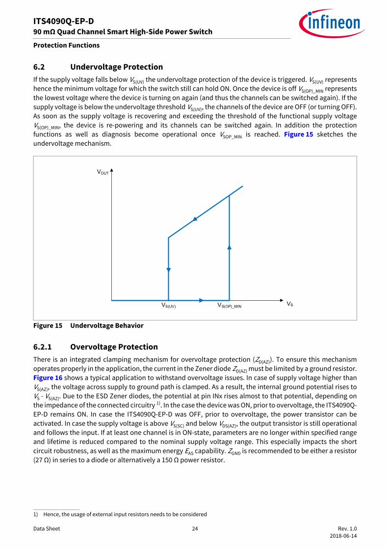
6.2 Undervoltage ProtectionIf the supply voltage falls below VS(UV) the undervoltage protection of the device is triggered. VS(UV) representshence the minimum voltage for which the switch still can hold ON. Once the device is off VS(OP)_MIN representsthe lowest voltage where the device is turning on again (and thus the channels can be switched again). If thesupply voltage is below the undervoltage threshold VS(UV), the channels of the device are OFF (or turning OFF).As soon as the supply voltage is recovering and exceeding the threshold of the functional supply voltageVS(OP)_MIN, the device is re-powering and its channels can be switched again. In addition the protectionfunctions as well as diagnosis become operational once VSOP_MIN is reached. Figure 15 sketches theundervoltage mechanism.
Figure 15 Undervoltage Behavior
6.2.1 Overvoltage ProtectionThere is an integrated clamping mechanism for overvoltage protection (ZD(AZ)). To ensure this mechanismoperates properly in the application, the current in the Zener diode ZD(AZ) must be limited by a ground resistor.Figure 16 shows a typical application to withstand overvoltage issues. In case of supply voltage higher thanVS(AZ), the voltage across supply to ground path is clamped. As a result, the internal ground potential rises toVS - VS(AZ). Due to the ESD Zener diodes, the potential at pin INx rises almost to that potential, depending onthe impedance of the connected circuitry 1). In the case the device was ON, prior to overvoltage, the ITS4090Q-EP-D remains ON. In case the ITS4090Q-EP-D was OFF, prior to overvoltage, the power transistor can beactivated. In case the supply voltage is above VS(SC) and below VDS(AZ), the output transistor is still operationaland follows the input. If at least one channel is in ON-state, parameters are no longer within specified rangeand lifetime is reduced compared to the nominal supply voltage range. This especially impacts the shortcircuit robustness, as well as the maximum energy EAS capability. ZGND is recommended to be either a resistor(27 Ω) in series to a diode or alternatively a 150 Ω power resistor.
1) Hence, the usage of external input resistors needs to be considered
VOUT
VSVS(UV) VS(OP)_MIN

Data Sheet 25 Rev. 1.0 2018-06-14
ITS4090Q-EP-D90 mΩ Quad Channel Smart High-Side Power Switch
Protection Functions
Figure 16 Overvoltage Protection with External Components
ITS4090Q-EP-D
OUTx
INx
VS
Logic
GND
ZDS(AZ)
IOUT
ZGND
ZD(AZ)ST
RIN
RST
+-
ISOV

Data Sheet 26 Rev. 1.0 2018-06-14
ITS4090Q-EP-D90 mΩ Quad Channel Smart High-Side Power Switch
Protection Functions
6.3 Reverse Polarity ProtectionIn case of reverse polarity, the intrinsic body diodes of the affected power DMOS channels will dissipate power.The current flowing through the intrinsic body diode is limited externally by the load itself. But in addition thecurrent into the ground path and the logic pins must be limited by an external resistor to the maximumallowed current described in Chapter 4.1. Figure 17 shows a typical application. ZGND resistor is used to limitthe current through the Zener protection of the device. ZGND is recommended to be either a resistor (~ 27 Ω) inseries to a diode or alternatively a power resistor (~ 150 Ω).During reverse polarity no protection functions are available.
Figure 17 Reverse Polarity Protection with External Components
ITS4090Q-EP-D
OUTx
INx
VS
Logic
GND
ZDS(AZ)
ZGND
ZD(AZ)ST
RIN
RST
VDS(REV)
+-
MicrocontrollerProtection
diodes
-VS(REV)
Data Sheet 27 Rev. 1.0 2018-06-14
ITS4090Q-EP-D90 mΩ Quad Channel Smart High-Side Power Switch
Protection Functions
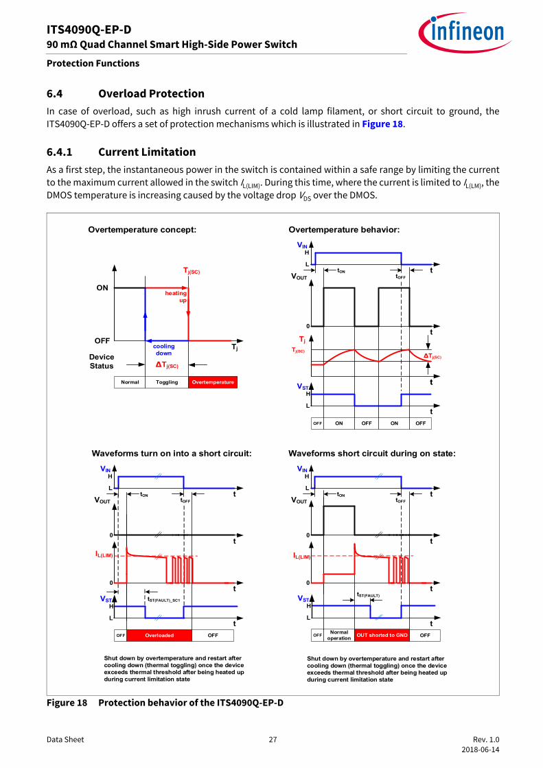
6.4 Overload ProtectionIn case of overload, such as high inrush current of a cold lamp filament, or short circuit to ground, theITS4090Q-EP-D offers a set of protection mechanisms which is illustrated in Figure 18.
6.4.1 Current LimitationAs a first step, the instantaneous power in the switch is contained within a safe range by limiting the currentto the maximum current allowed in the switch IL(LIM). During this time, where the current is limited to IL(LM), theDMOS temperature is increasing caused by the voltage drop VDS over the DMOS.
Figure 18 Protection behavior of the ITS4090Q-EP-D
Overtemperature concept: Overtemperature behavior:
OvertemperatureTogglingNormal
Waveforms turn on into a short circuit: Waveforms short circuit during on state:
t t
OFFOFF Overloaded OUT shorted to GNDOFF Normaloperation
ON
Tj(SC)
∆Tj(SC)
VOUT
t
t
0
IL(LIM)
0
Shut down by overtemperature and restart after cooling down (thermal toggling) once the device exceeds thermal threshold after being heated up during current limitation state
Shut down by overtemperature and restart after cooling down (thermal toggling) once the device exceeds thermal threshold after being heated up during current limitation state
VOUT
t
VIN
Lt
0
IL(LIM)
0
t
OFFOFF ON ON
VOUT
t
t
0
Tj
t
Tj(SC)∆Tj(SC)
OFF
TjOFF
cooling down
heating up
DeviceStatus
L
HVST
t
HVIN
L
H
L
HVST
t
tST(FAULT)_SC1
VIN
L
H
L
HVST
t
tST(FAULT)
tONtOFF
tONtOFF
tONtOFF
OFF
Data Sheet 28 Rev. 1.0 2018-06-14
ITS4090Q-EP-D90 mΩ Quad Channel Smart High-Side Power Switch
Protection Functions
6.4.2 Temperature Limitation in the Power DMOSEach channel incorporates one temperature sensor. Activation of this temperature sensor will cause anoverheated channel to switch OFF to prevent destruction. Any protective overtemperature shutdown eventtriggered within a channel is switching OFF the output of the corresponding channel until the temperaturereaches an acceptable value again.A restart functionality is implemented that is switching the channel ON again after the DMOS temperature hassufficiently cooled down.
6.5 Electrical Characteristics: Protection Functions
Table 5 Electrical Characteristics: Protection Functions 1)
VS = 8 V to 36 V, Tj = -40°C to 150°C (unless otherwise specified). Typical values are given at VS = 24 V, Tj = 25°C
1) Exposure to absolute maximum rating conditions for extended periods may affect device reliability. Integrated protection functions are designed to prevent IC from destruction under fault conditions described in the data sheet. Fault conditions are considered as “outside” normal operating range. Protection functions are designed neither for continuous nor repetitive operation.
Parameter Symbol Values Unit Note or Test Condition
NumberMin. Typ. Max.
Loss of GroundOutput leakage current while GND disconnected
IOUT(GND) – 0.1 – mA 2) 3) VS = 24 V
2) All pins are disconnected except VS and OUT.3) Not subject to production test; specified by design.
P_6.5.1
Reverse PolarityDrain source diode voltage during reverse polarity
VDS(REV) – 650 700 mV IL = -2 A Tj = 150°C
P_6.5.2
OvervoltageOvervoltage protection VS(AZ) 65 70 75 V 4) ISOV = 5 mA
4) For practical cases it is recommended to place a resistor in the range of ≥ 27 Ω into the GND path to limit the GND current associated with overvoltage events.
P_6.5.3
Overload ConditionLoad current limitation IL(LIM) 1.2 1.5 1.8 A – P_6.5.4
Thermal shutdown temperature
Tj(SC) 150 175 200 °C 3) – P_6.5.6
Thermal shutdown hysteresis
ΔTj(SC) – 30 – K 3) – P_6.5.7

Data Sheet 29 Rev. 1.0 2018-06-14
ITS4090Q-EP-D90 mΩ Quad Channel Smart High-Side Power Switch
Protection Functions
6.6 Typical Performance Characteristics Protection Functions
Typical Performance Characteristics
Current Limit IL(LIM) versusJunction Temperature Tj
Clamping Voltage VS(AZ) versusVoltage Tj
−50 0 50 100 1500
0.2
0.4
0.6
0.8
1
1.2
1.4
1.6
1.8
2
Tj [°C]
I L(LI
M) [A
]
VDS = 12V
−50 0 50 100 15065
66
67
68
69
70
71
72
73
74
75
Tj [°C]
VS
(AZ
) [V]
Data Sheet 30 Rev. 1.0 2018-06-14
ITS4090Q-EP-D90 mΩ Quad Channel Smart High-Side Power Switch
Diagnostic Functions
7 Diagnostic FunctionsFor diagnosis purpose, the ITS4090Q-EP-D provides a digital signal at pin ST. This signal is called STATUS. TheSTATUS pin is realized as open drain output and must be connected to an external pull-up resistor. Duringnormal operation the STATUS signal is logic “High” (H). During short circuit to ground or overtemperaturecondition the STATUS signal is logic “Low” (L). Table 6 shows the corresponding truth table.
7.1 Electrical Characteristics: Diagnostic Functions
Table 6 Diagnostic Truth Table 1) 2)
1) Please refer to Table 7 for more details.2) Not subject to production test; specified by design.
Device Operation INX all INi except INX OUTX all OUTi except OUTX ST CommentNormal Operation L L OFF OFF H 3) External pull
up at ST pin
3) “X” denotes status of OUTi according to the status of the corresponding input signals INi.
H H ON ON H
H don’t care ON X H
L don’t care OFF X H
Short Circuit to GND H don’t care ON X L 3) 4)
4) Device not in specified RDS(ON).
Overtemperature H don’t care OFF 5)
5) Channel remains off during cooling-down phase of power stage; then channel tries to re-start.
X L 3)
Table 7 Electrical Characteristics: Diagnostic FunctionsVS = 8 V to 36 V, Tj = -40°C to 150°C (unless otherwise specified). Typical values are given at VS = 24 V, Tj = 25°C
Parameter Symbol Values Unit Note or Test Condition
NumberMin. Typ. Max.
Diagnostic Timing in Overload ConditionSTATUS settling time for overload detection
tST(FAULT) – 30 – µs 1) VS = 24 V;load jump of RL: 47Ω -> 12 Ω;Please refer to Figure 18 for more details
P_7.1.1
STATUS settling time for channel start-up into existing overload 2)
tST(FAULT)_SC1 – 20 90 µs VDS ≥ 8 V;Please refer to Figure 18 for more details
P_7.1.9
“Low” level STATUS voltage VST(L) – – 0.5 V IST = 1.6 mA 3) P_7.1.3
“High” level STATUS voltage VST(H) 2 – – 4) V VS > VST3) P_7.1.4
Current through STATUS pin (Operating Range)
IST – – 1.6 mA VST < 0.5 V P_7.1.5

Data Sheet 31 Rev. 1.0 2018-06-14
ITS4090Q-EP-D90 mΩ Quad Channel Smart High-Side Power Switch
Diagnostic Functions
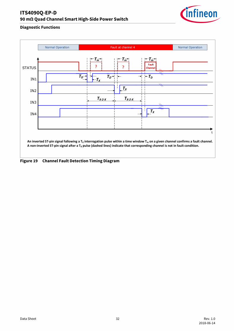
7.2 Channel Fault DetectionThe ITS4090Q-EP-D is equipped with an intelligent channel fault detection system, which allows with the aidof a microcontroller to identify and communicate the channel on which the fault occurs.During normal operation the STATUS pin is kept “High” by the external pull-up resistor as shown in Table 6. If - in case of a fault - the application requires the information on which of the channels the fault occurs whena “Low” STATUS is flagged, then the microcontroller can be programmed according to the sequence depictedas an example in Figure 19. The figure shows a case where three channels are active (these are channels 1, 2and 4). Channel 3 in this example is not switched ON. During normal operation of channels 1, 2 and 4 theSTATUS signal is “High”. If a fault occurs, e.g. at channel 4, the STATUS signal goes “Low” to flag an error to themicrocontroller. The microcontroller, in order to identify on which channel the fault occurs, must send a“Low” pulse sequentially to the input of each active channel, that is channels 1, 2 and 4 in this case. Thesepulses are shown in Figure 19 and their width is denominated Tx. The pulse width Tx should be between 3 µsup to 6 µs in order to make sure that the output does not react to this short inversion input level. The STATUSsignal will go to “High” for a short period of time Tmonly after the channel on which the fault occurs gets a“Low” pulse from the microcontroller, which in this case is after channel 4 receives a “Low” pulse for a time Tx.In this way, by reading back whether an inversion of the STATUS flag within Tm occurs, the microcontroller isable to detect on which channel the fault occurs. Once the microcontroller receives this information it canstart to switch OFF the channel on which the fault occurs (channel 4 in this case) via the corresponding inputpin. For the delay time TD between Tx going “Low” and Tm going “High” a value of 8 µs needs to be taken intoaccount.
Channel fault detection interrogation time (Sequential Pulse Width)
Tx 3 – 6 µs VST < 0.5 V 5) P_7.1.2
STATUS signal “High” valid window after Tx on fault affected channel
Tm 40 80 150 µs 5) – P_7.1.6
Minimum delay between subsequent Tx interrogation windows.
TX-2-X 200 – – µs 1) – P_7.1.8
Maximum delay time between Tx (“High” to “Low”) on fault affected channel and STATUS “High” signal Tm
TD – 8 – µs 1) – P_7.1.7
1) Not subject to production test; specified by design.2) This parameter describes the status settling time when a channel is switched on into an already existing overload
condition. This parameter is referenced to the edge of the input pin IN that switches the channel into overload.3) Levels referenced to device ground.4) Depends on pull-up circuit that is used within application; maximum ratings of STATUS pin need to be respected.5) Please refer to “Channel Fault Detection” on Page 31 for more details.
Table 7 Electrical Characteristics: Diagnostic Functions (cont’d)VS = 8 V to 36 V, Tj = -40°C to 150°C (unless otherwise specified). Typical values are given at VS = 24 V, Tj = 25°C
Parameter Symbol Values Unit Note or Test Condition
NumberMin. Typ. Max.
Data Sheet 32 Rev. 1.0 2018-06-14
ITS4090Q-EP-D90 mΩ Quad Channel Smart High-Side Power Switch
Diagnostic Functions
Figure 19 Channel Fault Detection Timing Diagram
IN1
IN2
IN3
IN4
STATUS
Fault at channel 4
TX
TX
TX
t
Normal Operation Normal Operation
TDTD TD
? ?
TX-2-X TX-2-X
Tm Tm Tm Fault
Channel
An inverted ST-pin signal following a TX interrogation pulse within a time window Tm on a given channel confirms a fault channel. A non-inverted ST-pin signal after a TX pulse (dashed lines) indicate that corresponding channel is not in fault condition.

Data Sheet 33 Rev. 1.0 2018-06-14
ITS4090Q-EP-D90 mΩ Quad Channel Smart High-Side Power Switch
Diagnostic Functions
7.3 Typical Performance Characteristics Diagnostic Functions
Typical Performance Characteristics
Status Settling Time tST(FAULT) versusJunction Temperature Tj (overload during ON)
Status Settling Time tST(Fault)_SC1 versusJunction Temperature Tj (switch on into overload)
Maximum Delay Time TD (TX ‘H->L’ to ST ‘L->H’) vs.Junction Temperature Tj
ST “High” Valid window (after TX) TM versusJunction Temperature Tj
−50 0 50 100 1500
10
20
30
40
50
60
70
80
Tj [°C]
t ST
(Fau
lt) [u
s]
VS = 24V
typ. t ST(Fault) for R L: 47 Ω −> 12 Ω
typ. t ST(Fault) for R L: 47 Ω −> 0 Ω
−50 0 50 100 1500
10
20
30
40
50
60
70
80
Tj [°C]
t ST
(Fau
lt)_S
C1 [u
s]
VS = 24V VDS = 8V
tST(Fault)_SC1
−50 0 50 100 1500
1
2
3
4
5
6
7
8
9
10
Tj [°C]
T D [u
s]
VS = 24V
TD
−50 0 50 100 1500
10
20
30
40
50
60
70
80
90
100
Tj [°C]
T M [u
s]
VS = 24V
TM

Data Sheet 34 Rev. 1.0 2018-06-14
ITS4090Q-EP-D90 mΩ Quad Channel Smart High-Side Power Switch
Input Pins
8 Input Pins
8.1 Input CircuitryThe input circuitry is compatible with 3.3 V and 5 V microcontrollers as well as input levels up to VS
1). Theconcept of the input pin is to react to voltage thresholds which are referenced to device ground. Animplemented Schmitt trigger avoids any undefined state if the voltage on the input pin is slowly increasing ordecreasing. The output is either OFF or ON but cannot be in a linear or undefined state. Figure 20 shows theelectrical equivalent input circuitry. In case a channel is permanently not needed, the corresponding input pinshall not be left floating but tied with a serial resistor to device ground (not module ground). Therecommended value for the serial resistor is 2.2 kΩ.
Figure 20 Input Pin Circuitry
8.2 Input Pin VoltageThe input pin IN uses a comparator with hysteresis. Switching “ON / OFF” of the channels takes place in adefined region, set by the thresholds VIN(L),max and VIN(H),min. The exact values where the “ON” and “OFF” take
1) VIN must not exceed VS. The relation VIN ≤ VS must always be fulfilled.
ITS4090Q-EP-D
OUTx
INx
Device Logic
Gate Driver
GND
Bias
ZGND
Inv.Comp
VS
VIH
Data Sheet 35 Rev. 1.0 2018-06-14
ITS4090Q-EP-D90 mΩ Quad Channel Smart High-Side Power Switch
Input Pins
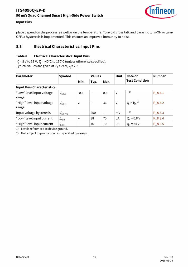
place depend on the process, as well as on the temperature. To avoid cross talk and parasitic turn-ON or turn-OFF, a hysteresis is implemented. This ensures an improved immunity to noise.
8.3 Electrical Characteristics: Input Pins
Table 8 Electrical Characteristics: Input PinsVS = 8 V to 36 V, Tj = -40°C to 150°C (unless otherwise specified). Typical values are given at VS = 24 V, Tj = 25°C
Parameter Symbol Values Unit Note or Test Condition
NumberMin. Typ. Max.
Input Pins Characteristics“Low” level input voltage range
VIN(L) -0.3 – 0.8 V – 1)
1) Levels referenced to device ground.
P_8.3.1
“High” level input voltage range
VIN(H) 2 – 36 V VS > VIN1) P_8.3.2
Input voltage hysteresis VIN(HYS) – 250 – mV – 2)
2) Not subject to production test; specified by design.
P_8.3.3
“Low” level input current IIN(L) – 38 70 µA VIN = 0.8 V P_8.3.4
“High” level input current IIN(H) – 46 70 µA VIN = 24 V P_8.3.5

Data Sheet 36 Rev. 1.0 2018-06-14
ITS4090Q-EP-D90 mΩ Quad Channel Smart High-Side Power Switch
Input Pins
8.4 Typical Performance Characteristics Input Pins
Typical Performance Characteristics
Input Voltage thresholds VIN(L) VIN(H) versusJunction Temperature Tj
Input Voltage hysteresis VIN(HYS) versusJunction Temperature Tj
Input Pin Current IIN(H) versusSupply Voltage V S
Input Pin Current IIN(H) versusJunction Temperature Tj
0 50 100 1500
0.2
0.4
0.6
0.8
1
1.2
1.4
1.6
1.8
2
Tj [°C]
VIN
[V]
VS = 24V
VIN(H)
VIN(L)
0 50 100 1500
0.1
0.2
0.3
0.4
0.5
0.6
0.7
0.8
Tj [°C]
VIN
[V]
VS = 24V
VIN(HYS)
0 5 10 15 20 250
10
20
30
40
50
60
70
VIN [V]
I IN [u
A]
VS = 28.8V
Tj −40°C
Tj 25°C
Tj 150°C
0 50 100 1500
10
20
30
40
50
60
70
Tj [°C]
I IN [u
A]
VIN = 24V

Data Sheet 37 Rev. 1.0 2018-06-14
ITS4090Q-EP-D90 mΩ Quad Channel Smart High-Side Power Switch
Application Information
9 Application Information
9.1 Application Diagram
Note: This is a very simplified example of an application circuit. The function must be verified in the real application.
Figure 21 Application Diagram with ITS4090Q-EP-D
In Figure 21 above a simplified application diagram is shown where the inputs are galvanically isolated fromVS with optocouplers. Thanks to the fact that the input pins are 24 V capable they can be directly connected tothe optocouplers. Reverse polarity protection can be achieved with external components. In this context itshould be noted that input pins of channels which are permanently unused have to be tied with 2.2 kΩresistance to device ground. In addition the TM-pin must be always be tied with a serial resistor to deviceground in order to protect the pin in case of reverse polarity. The recommended value for this serial resistor isalso 2.2 kΩ. For applications where no galvanic isolation is present between the external control circuitry (e.gmicrocontroller) and the input pins of the ITS4090Q-EP-D serial input resistors need to be placed in order to
ITS4090Q-EP-D
IN1
VS
GND
ST
Microcontrollere.g. XMC4xxx
IN2
IN3
IN4
OUT1
OUT2
OUT3
OUT4
I/O
I/O
I/O
I/O
I/O
GND
LOA
D 1
LOA
D 2
VDD
Linear Voltage Regulator
e.g. IFX1763
VOUT VIN
COUT
LOA
D 3
LOA
D 4
VDD
External components for Surge Immunity
VS
ZGND
External components for reverse polarity protection and overvoltage pulses. Recommended setup for ZGND is a diode for reverse polarity in series with a resistor of ~27Ω to limit GND current during overvoltage spikes.
TM
2.2 kΩ
30 kΩ

Data Sheet 38 Rev. 1.0 2018-06-14
ITS4090Q-EP-D90 mΩ Quad Channel Smart High-Side Power Switch
Application Information
protect the external control circuitry and the input structures of the ITS4090Q-EP-D under fault conditions(like e.g. reverse polarity, loss of ground or overvoltage). For further details please also refer to thecorresponding sections in Chapter 6. The recommended value for such serial input resistors is 10 kΩ howeverapplication specific optimized values may also depend on the individual application conditions as well as theapplied external control circuitry / microcontroller.
9.2 Thermal ConsiderationsIf the cooling possibilities within the application are not sufficient to sink the heat of the dissipated power thejunction temperature Tj of the device may exceed its maximum specified rating of 150°C and eventually triggera thermal shutdown of the overheated channels to protect the device from destruction. Such thermalshutdown events may occur e.g. if one or more channels are operated in overload conditions that are causingthe current limitation functionality to become active. If the current limitation of a channel becomes active thepower dissipation will rise rapidly and in many cases lead to thermal shutdown events of the correspondingchannels within short periods of time. But also under nominal load conditions the power dissipation can become too high inside an application if itis applied at high environmental temperature TAMB and if at the same time the cooling capability of the PCB isnot sufficient (thanks to the very good RDSON performance of the ITS4090Q-EP-D this restriction is limited tocases with poor thermal connection to the PCB being applied at very high ambient temperatures TAMB as willbe shown below). In general the cooling capability of an IC on a PCB within an application can be described forstatic cases by its thermal resistance from junction-to-ambient RthJA. The thermal resistance RthJA can beimproved by adding cooling area on top- or bottom layer of the PCB or by adding inner layers that areconnected to the VS layer with thermal vias. Thermal vias show the best efficiency for heat distribution ifdirectly placed underneath the exposed pad of the ITS4090Q-EP-D. The achievable values for RthJA will differfrom application to application. As reference simulation values of RthJA for a set of standardized JEDEC casesare provided in Chapter 4.4 “Thermal Resistance” on Page 12. Actual values in real applications naturallycan be lower or higher.For cases where the achievable thermal resistance RthJA and the hereof resulting thermal budget within anapplication is not sufficient for a given ambient temperature TAMB there is no other choice than to lower theload current to smaller numbers than the allowed maximum nominal current of 750 mA. Figure 22 illustrateshow the derating of the nominal current due to excessive power dissipation can look like as a function ofachievable RthJA and given TAMB. The graphs show how the thermal budget with its limiting condition Tj = 150°Ccan be shared between the influencing parameters TAMB, RthJA, ILoad depending on the number of activechannels nCH. Due to the excellent ratio of RDSON versus nominal load current this impact shown in thementioned figures below are relevant only for worst case scenarios like RthJA of “footprint only” where noadditional cooling is present at all but solely footprint and PCB traces to the pins of the device. Even undersuch harsh conditions the only noteworthy limitations occur for TAMB > 75°C if all four channels are operatedat full load. An arbitrary RthJA value of 100 K/W is depicted in addition and may serve as an RthJA - referencevalue for which derating may become relevant when being exposed to high ambient temperatures ofTAMB = 85°C and above.The calculation of the thermal budget displayed in the graphs follows simple rules as given in the equationsbelow. It should be noted that the calculation is restricted to static cases where the resulting TAMB and Tj havereached a stable equilibrium.
(9.1)
(9.2)
Tj = TAMB + RthJA × PDISS
PDISS = ILoad2 × RDS(ON) × nCH + VS × IGND

Data Sheet 39 Rev. 1.0 2018-06-14
ITS4090Q-EP-D90 mΩ Quad Channel Smart High-Side Power Switch
Application Information
Figure 22 Possible thermal derating of nominal current due to insufficient cooling capability of PCB
20 30 40 50 60 70 80 90 1000
100
200
300
400
500
600
700
800
TAMB [°C]
I nom
,max
[mA
]
3 channels active (VS = 28V)
RthJA = 100 K/W
RthJA = 119 K/W
20 30 40 50 60 70 80 90 1000
100
200
300
400
500
600
700
800
TAMB [°C]
I nom
,max
[mA
]
4 channels active (VS = 28V)
RthJA = 100 K/W
RthJA = 119 K/W

Data Sheet 40 Rev. 1.0 2018-06-14
ITS4090Q-EP-D90 mΩ Quad Channel Smart High-Side Power Switch
Package Outlines
10 Package Outlines
Figure 23 PG-TSDSO-14 (Plastic Dual Small Outline Package) (RoHS-Compliant)
Green Product (RoHS compliant)To meet the world-wide customer requirements for environmentally friendly products and to be compliantwith government regulations the device is available as a green product. Green products are RoHS-Compliant(i.e Pb-free finish on leads and suitable for Pb-free soldering according to IPC/JEDEC J-STD-020).
For further information on alternative packages, please visit our website:http://www.infineon.com/packages. Dimensions in mm

Data Sheet 41 Rev. 1.0 2018-06-14
ITS4090Q-EP-D90 mΩ Quad Channel Smart High-Side Power Switch
Revision History
11 Revision History
Revision Date Changes1.0 2018-06-14 Data Sheet (Initial Release)

IMPORTANT NOTICEThe information given in this document shall in noevent be regarded as a guarantee of conditions orcharacteristics ("Beschaffenheitsgarantie"). With respect to any examples, hints or any typicalvalues stated herein and/or any information regardingthe application of the product, Infineon Technologieshereby disclaims any and all warranties and liabilitiesof any kind, including without limitation warranties ofnon-infringement of intellectual property rights of anythird party. In addition, any information given in this document issubject to customer's compliance with its obligationsstated in this document and any applicable legalrequirements, norms and standards concerningcustomer's products and any use of the product ofInfineon Technologies in customer's applications. The data contained in this document is exclusivelyintended for technically trained staff. It is theresponsibility of customer's technical departments toevaluate the suitability of the product for the intendedapplication and the completeness of the productinformation given in this document with respect tosuch application.
For further information on technology, delivery termsand conditions and prices, please contact the nearestInfineon Technologies Office (www.infineon.com).
Please note that this product is not qualifiedaccording to the AEC Q100 or AEC Q101 documents ofthe Automotive Electronics Council.
WARNINGSDue to technical requirements products may containdangerous substances. For information on the typesin question please contact your nearest InfineonTechnologies office.
Except as otherwise explicitly approved by InfineonTechnologies in a written document signed byauthorized representatives of Infineon Technologies,Infineon Technologies’ products may not be used inany applications where a failure of the product or anyconsequences of the use thereof can reasonably beexpected to result in personal injury.
TrademarksAll referenced product or service names and trademarks are the property of their respective owners.
Edition 2018-06-14Published by Infineon Technologies AG81726 Munich, Germany
© 2018 Infineon Technologies AG.All Rights Reserved.
Do you have a question about any aspect of this document?Email: [email protected]