infra-red investigation on silicon solar cells · si wafer has to go through cleaning process,...
TRANSCRIPT
Malaysian Journal of Analytical Sciences, Vol 21 No 5 (2017): 1134 - 1142
DOI: https://doi.org/10.17576/mjas-2017-2105-16
1134
MALAYSIAN JOURNAL OF ANALYTICAL SCIENCES
Published by The Malaysian Analytical Sciences Society
INFRA-RED INVESTIGATION ON SILICON SOLAR CELLS
(Kajian Inframerah ke atas Sel-sel Suria Silikon)
Nurfarizza Surhada Mohd Nasir, Suhaila Sepeai*, Cheow Siu Leong, Kamaruzzaman Sopian, Saleem H.Zaidi
Solar Energy Research Institute (SERI)
Universiti Kebangsaan Malaysia, 43600 UKM Bangi, Selangor, Malaysia
*Corresponding author: [email protected]
Received: 12 April 2017; Accepted: 1 September 2017
Abstract
Increasing reliance on carbon-based fossil fuel is likely to cause irreversible damage to global environment. Crystalline silicon
(Si) based on pollution free photovoltaic (PV) electricity generation technology is expected to play a dominant role in this
electricity generation transition from carbon to silicon. Since Si wafer represents almost 50% of the PV conversion cost, thinner
wafers are highly effective at reducing the production cost. Therefore, there is an urgent need to develop alternative device
configurations and processing methods for thinner Si wafer. Si wafer has to go through cleaning process, thinning process,
textured process and partially transparent technique. In this work optical transmission through Si is investigated as a function of
wafer thickness. For this improved performance, surface morphology, optical properties and the optical transmission near band
gap is measured with custom-designed rear infra-red (IR) transmission measurement system. Si wafer with the textured surface
have more light absorption than the as-cut and planar Si wafer.
Keywords: optical transmission, thin silicon wafers, infrared light, light absorption
Abstrak
Peningkatan kebergantungan terhadap penggunaan bahan bakar berasaskan sumber karbon mengakibatkan pencemaran alam
sekitar. Fotovolta (PV) sifar pencemaran berasaskan silikon kristal merupakan teknologi tenaga elektrik generasi terkini
dijangkakan menjadi sumber yang mendominasi perubahan sumber bahan api berasaskan karbon kepada silikon. Tambahan pula,
kepingan silikon meliputi 50% kos keseluruhan pembuatan PV, pengurangan kos yang efektif didapati melalui penipisan
kepingan.. Oleh itu, kaedah alternatif kepada pembaharuan bagi konfigurasi sistem penipisan silikon harus di cadangan.
Kepingan silikon harus melalui proses pembersihan, proses penipisan, proses tekstur dan teknik separa telus. Dalam kajian
hubungan di antara ketebalan kepingan silicon dan maklumat optik diteliti. Bagi meningkatkan prestasi, morfologi permukaan,
sifat optik, dan penghantaran optik menghampiri jurang jalur diukur dengan menggunakan sistem pengukuran penghantaran
gelombang IR.
Kata kunci: penghantaran optik, kepingan silikon nipis, cahaya inframerah, penyerapan cahaya
Introduction
Silicon wafer-based photovoltaic module production has been growing over 30% since the last decade [1].
Generally, the cost of Si accounts for almost 50% of a photovoltaic panel [2]. Historically, a pathway to reduce cost
has been realized by economic use of Si in the form of thinner substrates; current Si wafer is in 150 – 200 𝜇m
thickness [3]. Si PV technology is almost exclusive based on mono-facial solar cells in which light is incident from
the front surface with the back surface completely metallized. The bifacial solar cell is an emerging solar cell
configuration in which electrical grid patterns are identical on both front and back surfaces. This device
ISSN
1394 - 2506
Nurfarizza Surhada et al: INFRA-RED INVESTIGATION ON SILICON SOLAR CELLS
1135
configuration has the potential to generate more power by capturing scattered light from the rear surface than the
mono-facial solae cell. The challenging problems in bifacial solar cell is to ensure that the photo-generated electron-
hole (ē-h) pairs absorbed near the back surface are collected by the front surface emitter prior to recombination.
This experiment can be done by using appropriate surface texturing methods, light trapping can be enhanced and
absorption in the rear-infrared (NIR) [4-6]. The optical properties of a broad range of different bifacial
configurations with varying surface morphologies and rear side reflectors have been extensively investigated in the
literature. Although wafer thickness reduction translates into smaller recombination losses and large open circuit
voltages; absorption is reduced as well [7].
These considerations have led to extensive research on performance limiting factors in amorphous [8], multi-
crystalline [9], and single crystalline solar cells [10, 11]. Due to its indirect band gap, crystalline silicon has weak
optical absorption particularly in the range (~900 – 1100) nm. Therefore, in solar cell studies aimed at increasing the
efficiency, the primary goal is to enhance light absorption while minimizing recombination losses. Surface texturing
aimed at enhanced absorption in silicon has been extensively investigated by geometrical optic [12]. Geometrical
textures reduce reflection light into the semiconductor. Despite their effectiveness and industrial applications,
geometrical texturing schemes suffer from several disadvantages that limits their effectiveness. Some of those are
listed below [13]:
i) Wet-chemical alkaline anisotropic etching used to form random pyramids in (100) oriented crystal is not effective
in texturing of flow cost multi-crystalline (mc-Si) wafers, ii) Anti-reflection films have a resonant structure which
limits their effectiveness to a narrow range of angles and wavelength, iii) Sufficient IR absorption in thin film ( <
10 𝜇m) silicon solar cells is not possible with geometrical optics based texturing.
Light trapping schemes based on geometrical optics considerations have been developed for enhancing oblique
coupling beyond narrow angle range of (~16°) defined as 𝑠𝑖𝑛−1(1/n), where n is the refractive index of silicon [14].
In general, the required feature dimensions for geometrical optical path length enhancement are optical wavelength,
therefore their applicability to thinner wafers is impractical. Periodically textured surfaces based on diffractive [15]
and waveguide optics [16] have been shown to significantly enhance optical absorption. For a weakly absorptive
medium, statistical analysis by Yablonovitch [17] and optical analysis of scattering from a lambertian surface
predicted absorption enhancement in textured surfaces by (~4𝑛2) over a planar surface, where n is the refractive
index of the material. Absorption in such structure is opposed to conventional horizontal, thin-film waveguide
structures as proposed by Sheng [18].
In literature application of diffractive and physical optics structures aimed enhancement of optical absorption in thin
Si films and solar cells have been reported with good results [19 – 28]. Lambertian schemes and related geometrical
optics-based ray tracing approached were applied to both amorphous silicon [29] and crystalline silicon solar cells
[30] with successfully results. A lambertian surface capable of filling all the available k-space with light beams of
equal intensity is difficult to achieve in practice. A close approximation is a randomly textured surface supporting
sub-wavelength features. Therefore, the random surface can be described by Fourier summation-over a large
number of periods. Although the resulting diffractive scattering ensures almost complete filling of the k-space. Light
incident on such surfaces normally is diffractively scattered over a broad angular range determined by using
equation 1 below
𝜃m,i=sin−1(𝑚i𝜆/n𝑑i) (1)
where n, 𝑑i represents the 𝑚th diffraction order corresponding to the spatial period 𝑑i and n is Si refractive index.
Optical path length in geometrical optics is simply the sum of number of passes through a thin film of thickness, t.
For a single grating the total optical path length enhancement is given by summing over the lengths of all
transmitted diffraction order (equation 2):
𝑑optgrating
= ∑ 𝑖 𝛾i𝑑i (2)
Malaysian Journal of Analytical Sciences, Vol 21 No 5 (2017): 1134 - 1142
DOI: https://doi.org/10.17576/mjas-2017-2105-16
1136
where 𝛾i is fraction of incident energy coupled into diffractive, 𝑑i. For a normally propagating zero order, 𝑑0 is
identical to t; for the diffraction orders the optical path is t/cos 𝜃𝑖𝑗 where 𝜃i the angle of propagation of the 𝑖th
diffraction order. For a random sub-wavelength diffractive surface the total optical path length is summed over all
grating (i); each of which generates diffraction orders (j) as defined as (equation 3):
𝑑optrandom= ∑ 𝛾i,j𝑑i,ji,j (3)
Comparison of the three cases (planar, single period and random surface) illustrate that an appropriately designed
random surface is highly effective in filling the k-space and therefore in reaching the 4𝑛2 enhancement limit.
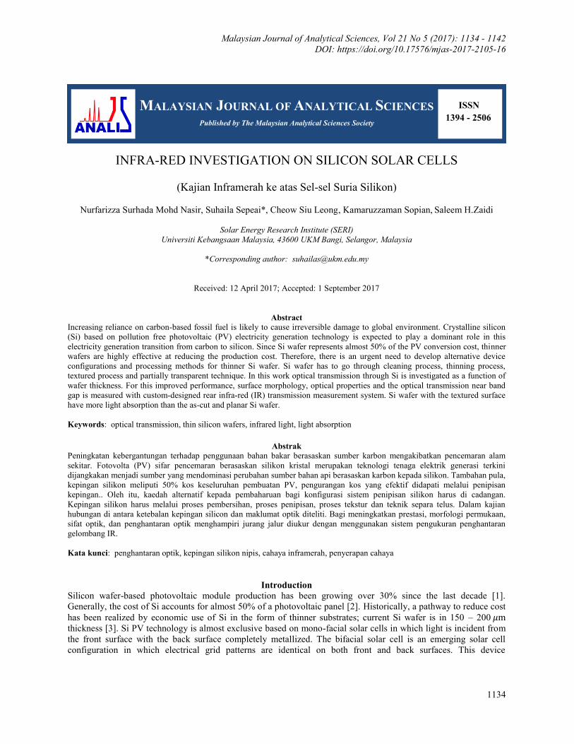
For a good solar cell it is crically important that all of the incident energy to be scattered into obliquely propagating
transmitted orders in order to enhance optical path length hence increase absorption rate. This can be achieved for
feature dimensions either substaintially larger (Figure. 1(a)) or comparable or substaintially smaller than optical
wavelength (Figure. 1 (b)). The first configuration refers to geometrical optics, the second to diffractive optics, and
the third to physical optics. In the physical optics approach deeply etched subwavelength structures are created in
three dimensions, on the surface and through the substrate. Rigorous coupled wave analysis [14] has been used to
calculate optical absorption in these 3D grating structures. Physical optics also described in terms of subwavelength
surfaces (sws) essentially acting as multi-layer anti-reflection films [31]. Structures play no role in optical path
length enhancement. In this paper, near IR transmission in (~800 – 1700) nm spectral range for planar and
randomly textured Si wafers have been investigated for Si wafers with thickness of (~200 𝜇m).
Figure 1. Schematic description of light, interaction with surface features (a) optical wavelength and (b) either or
optical wavelength for convenience reflected (diffracted beams are not shown).
Materials and Methods
Single crystalline silicon (c-Si) wafer with thickness about (~200 𝜇m) is used. P-type Si wafers with resistivity
ranging between (0.5-3.0) Ω.cm with doping density between 1010
to 1016
were used. The silicon (Si) wafer was
initially cleaned by dipping into solution of hydrofluoric acid (HF) and nitric acid (HNO3) in a ratio of 1:100 for 10
minutes. After rinsing with deionized water, it was then dipped into HF and water in a ratio of 1:50 for 1 minute.
The wafer was immersed in 10% potassium hydroxide (KOH) at a temperature of 70 – 80 ℃ for 5 minutes.
Subsequently, the wafer was repeatedly cleaned in HF:H2O for 1 minute. Then the wafers were rinsed with
deionized water for about 2 minutes and dried with nitrogen gas. Etching process led to the decrease in thickness of
Si wafers. Figure 2(a) shows an etching process by using KOH solution. Si wafer with damage removal needs to go
through the texturing process with ratio of 1:5:125. The texturing process is a combination of 4 g of KOH pallets,
20 ml of isopropanol and 90 ml of deionized ( DI ) water. The Si wafer will be laminated by using the laminator.
Then, the laminated wafer will be transferred into a beaker which contained 10% KOH solution.
The estimated time would be 1 hour and 45 minutes at the temperature of 70 – 80 ℃. Next, the IR transmission data
will be measured. Figure 2(b) shows the etching process by using HF:HNO3 with a ratio of 1:10. Then, Si wafer-
textured were dipped in a solution of HF:HNO3 with ratio of 1:10 for 1 hour and 45 minutes. Then, the wafers were
(a) (b)
Nurfarizza Surhada et al: INFRA-RED INVESTIGATION ON SILICON SOLAR CELLS
1137
rinsed and dried with nitrogen gas. The IR transmission data is recorded from (600 – 1200) nm wavelength with
sub-wavelength 25 nm. Figure 2(c) shows a process flow for paste Black Etching Surface (BES) paste process on
silicon wafer with 200 𝜇m thickness. Next, the oxidation process was applied to the Si wafers. The time estimated
to produce the oxide layer approach 350 Ǻ is 1 hour and 30 minutes at the temperature 1100 ℃. The Si wafers size
were then cut into 4 cm x 4 cm.The BES paste contains level of carbon black and n-methyl-2-pyrrolidone by EMD
Chemicals Company is placed onto the mask and at the same time the Si wafer is placed under the mask. After that,
the etched Si wafer is heated in the furnace at the temperature of 350 ℃ for 90 seconds. Next, Si wafer is soaked in
1% KOH for 1 minute at 40 ℃. After the BES paste is peeled out from the Si wafer, the Si wafer is placed into 10%
KOH solution for 1 hour and 15 minutes at 70 ℃. Then, the Si wafer is rinsed using deionized (DI) water and dried
with nitrogen gas.
Figure 2. (a) Process flow for KOH etching process on silicon wafer with 200−μm thickness (b) Process flow for
HF:HNO3 etching process on silicon wafer with 200−𝜇m thickness (c) Process flow for BES paste
process on silicon wafer with 200−𝜇m thickness.
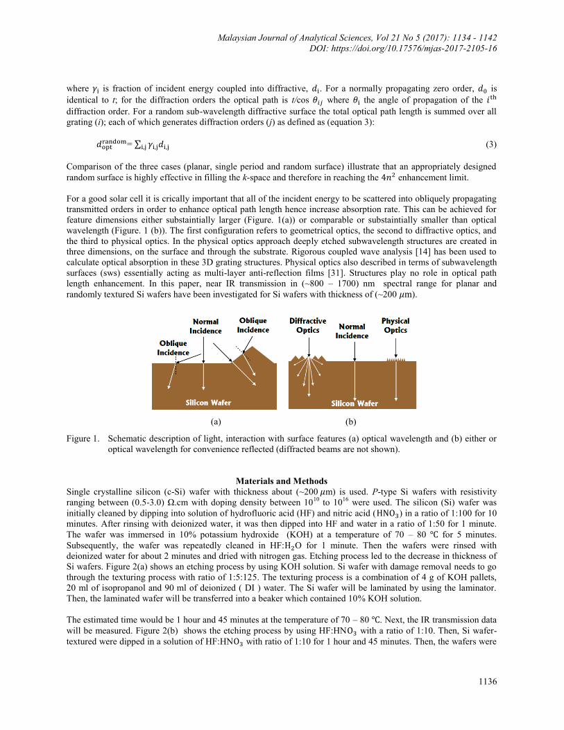
A simple experimental setup based on optical configuration described in Figure 3 has been developed for
characterization of near IR transmission as a function of wavelength. This system is designed to measure optical
transmission system in near and far infrared (IR) range specifically for the wavelength. A computer controlled IR
monochromator is used to vary wavelength in the desired range. Spectrally variable light from te monochromator is
incident normally on the sample under measurement (SUM). The transmitted light from the sum is collected
focusing lens onto an InGaAs photodetector. The output from photodetector is connected to a lock-in amplifier,
which is connected to a computer. Intensity variation as a function of wavelength is measured with a LABVIEW
based computer programme.
Figure 3. Schematic diagram for IR transmission measurement system
(a) (c) (b)

Malaysian Journal of Analytical Sciences, Vol 21 No 5 (2017): 1134 - 1142
DOI: https://doi.org/10.17576/mjas-2017-2105-16
1138
Results and Discussion
In order to reduce the reflectivity of the surface and to trap the light in solar cell, texturing process by using KOH
solution have developed good achievement in capturing the light.In this work, thining process include KOH etching
pocess whereas the Si wafers were immersed in 10 % KOH solution with different time eching such as 30, 60, 90
and 180 minutes. In figure. 4 shows the surface morphology from scanning electron microscope (SEM) analysis for
KOH-etched surface. Table 1 conclude that the SEM data at 30 minutes the Si wafer reduced to 58. 4 µm and the
etching rate is 1.94 µm/ min. Table 2 summarize from surface profiler at 30 minutes the Si wafer reduced to 31.24
µm and the etching rate is 1.04 𝜇m/min. These etch results show that etch rate is significantly slowed as etch time
increase, this may be attributted to loss of water in the solution to the evaporation resulting in a higher KOH
concentration which in turn, slow the etch rate.
Figure 4. Topographical images for KOH-etched Si surfaces for etching times of 30 minutes (a), 60 minutes (b),
90 minutes (c) and 180 minutes (d)
Table 1. Result of the thickness for KOH etching vs time from SEM data
Samples
(minutes)
Thickness
(𝝁𝐦)
Etching Rate
(𝝁𝐦/min)
30 58.4 1.94
60 41.3 0.63
90 97.3 1.08
180 135.2 0.75
Table 2. Result of the thickness for KOH etching vs time from surface profiler
Samples
(minutes)
Thickness
(𝝁𝐦)
Etching Rate
(𝝁𝐦/min)
30 31.238 1.04
60 58.056 0.96
90 91.862 1.02
180 213.18 1.18
Figure 5 shows Si wafer surface after through the KOH etching process. Etching of Si in orientation-dependent
alkaline solutions is very well characterized. The etch anisotropy of the alkaline solutions basically results from the
fewer surface Si-OH bonds per unit cell on <111> compared to <100> and <110> surfaces. Due to this, it leads to
higher energy to break bonds of the <111> surface Si atoms. This anisotropy effect is employed to generate V-
grooves in <100> Si wafers using openings in an appropriate mask such as an oxide layer. The wafer release two
(a) (b) (c) (d)
Nurfarizza Surhada et al: INFRA-RED INVESTIGATION ON SILICON SOLAR CELLS
1139
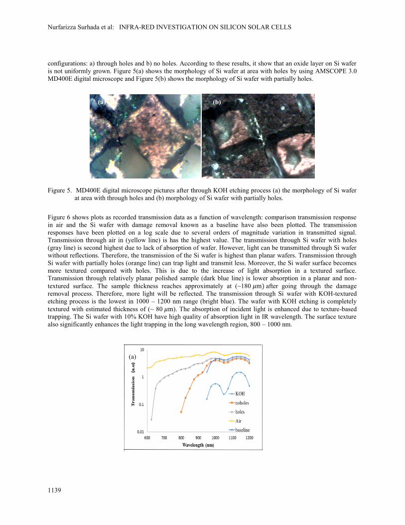
configurations: a) through holes and b) no holes. According to these results, it show that an oxide layer on Si wafer
is not uniformly grown. Figure 5(a) shows the morphology of Si wafer at area with holes by using AMSCOPE 3.0
MD400E digital microscope and Figure 5(b) shows the morphology of Si wafer with partially holes.
Figure 5. MD400E digital microscope pictures after through KOH etching process (a) the morphology of Si wafer
at area with through holes and (b) morphology of Si wafer with partially holes.
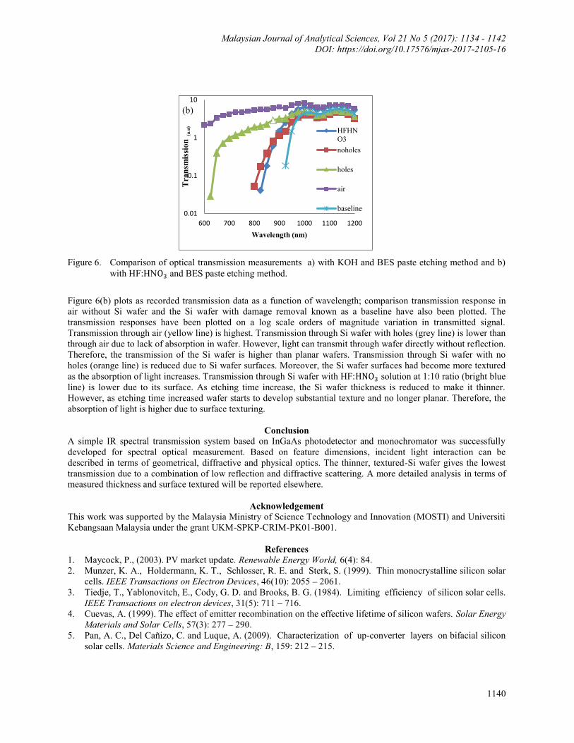
Figure 6 shows plots as recorded transmission data as a function of wavelength: comparison transmission response
in air and the Si wafer with damage removal known as a baseline have also been plotted. The transmission
responses have been plotted on a log scale due to several orders of magnitude variation in transmitted signal.
Transmission through air in (yellow line) is has the highest value. The transmission through Si wafer with holes
(gray line) is second highest due to lack of absorption of wafer. However, light can be transmitted through Si wafer
without reflections. Therefore, the transmission of the Si wafer is highest than planar wafers. Transmission through
Si wafer with partially holes (orange line) can trap light and transmit less. Moreover, the Si wafer surface becomes
more textured compared with holes. This is due to the increase of light absorption in a textured surface.
Transmission through relatively planar polished sample (dark blue line) is lower absorption in a planar and non-
textured surface. The sample thickness reaches approximately at (~180 𝜇m) after going through the damage
removal process. Therefore, more light will be reflected. The transmission through Si wafer with KOH-textured
etching process is the lowest in 1000 – 1200 nm range (bright blue). The wafer with KOH etching is completely
textured with estimated thickness of (~ 80 𝜇m). The absorption of incident light is enhanced due to texture-based
trapping. The Si wafer with 10% KOH have high quality of absorption light in IR wavelength. The surface texture
also significantly enhances the light trapping in the long wavelength region, 800 – 1000 nm.
(a) (b)
(a)
Malaysian Journal of Analytical Sciences, Vol 21 No 5 (2017): 1134 - 1142
DOI: https://doi.org/10.17576/mjas-2017-2105-16
1140
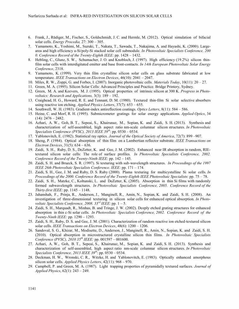
Figure 6. Comparison of optical transmission measurements a) with KOH and BES paste etching method and b)
with HF:HNO3 and BES paste etching method.
Figure 6(b) plots as recorded transmission data as a function of wavelength; comparison transmission response in
air without Si wafer and the Si wafer with damage removal known as a baseline have also been plotted. The
transmission responses have been plotted on a log scale orders of magnitude variation in transmitted signal.
Transmission through air (yellow line) is highest. Transmission through Si wafer with holes (grey line) is lower than
through air due to lack of absorption in wafer. However, light can transmit through wafer directly without reflection.
Therefore, the transmission of the Si wafer is higher than planar wafers. Transmission through Si wafer with no
holes (orange line) is reduced due to Si wafer surfaces. Moreover, the Si wafer surfaces had become more textured
as the absorption of light increases. Transmission through Si wafer with HF:HNO3 solution at 1:10 ratio (bright blue
line) is lower due to its surface. As etching time increase, the Si wafer thickness is reduced to make it thinner.
However, as etching time increased wafer starts to develop substantial texture and no longer planar. Therefore, the
absorption of light is higher due to surface texturing.
Conclusion
A simple IR spectral transmission system based on InGaAs photodetector and monochromator was successfully
developed for spectral optical measurement. Based on feature dimensions, incident light interaction can be
described in terms of geometrical, diffractive and physical optics. The thinner, textured-Si wafer gives the lowest
transmission due to a combination of low reflection and diffractive scattering. A more detailed analysis in terms of
measured thickness and surface textured will be reported elsewhere.
Acknowledgement
This work was supported by the Malaysia Ministry of Science Technology and Innovation (MOSTI) and Universiti
Kebangsaan Malaysia under the grant UKM-SPKP-CRIM-PK01-B001.
References
1. Maycock, P., (2003). PV market update. Renewable Energy World, 6(4): 84.
2. Munzer, K. A., Holdermann, K. T., Schlosser, R. E. and Sterk, S. (1999). Thin monocrystalline silicon solar
cells. IEEE Transactions on Electron Devices, 46(10): 2055 – 2061.
3. Tiedje, T., Yablonovitch, E., Cody, G. D. and Brooks, B. G. (1984). Limiting efficiency of silicon solar cells.
IEEE Transactions on electron devices, 31(5): 711 – 716.
4. Cuevas, A. (1999). The effect of emitter recombination on the effective lifetime of silicon wafers. Solar Energy
Materials and Solar Cells, 57(3): 277 – 290.
5. Pan, A. C., Del Cañizo, C. and Luque, A. (2009). Characterization of up-converter layers on bifacial silicon
solar cells. Materials Science and Engineering: B, 159: 212 – 215.
0.01
0.1
1
10
600 700 800 900 1000 1100 1200
Tra
nsm
issi
on
(a
.u)
Wavelength (nm)
HFHN
O3
noholes
holes
air
baseline
(b)
Nurfarizza Surhada et al: INFRA-RED INVESTIGATION ON SILICON SOLAR CELLS
1141
6. Frank, J., Rüdiger, M., Fischer, S., Goldschmidt, J. C. and Hermle, M. (2012). Optical simulation of bifacial
solar cells. Energy Procedia, 27: 300 – 305.
7. Yamamoto, K., Yoshimi, M., Suzuki, T., Nakata, T., Sawada, T., Nakajima, A. and Hayashi, K. (2000). Large-
area and high efficiency a-Si/poly-Si stacked solar cell submodule. In Photovoltaic Specialists Conference, 200
0. Conference Record of the Twenty-Eighth IEEE: pp. 1428 – 1432.
8. Hebling, C., Glunz, S. W., Schumacher, J. O. and Knobloch, J. (1997). High efficiency (19.2%) silicon thin-
film solar cells with interdigitated emitter and base front-contacts. In 14th European Photovoltaic Solar Energy
Conference, 2318.
9. Yamamoto, K. (1999). Very thin film crystalline silicon solar cells on glass substrate fabricated at low
temperature. IEEE Transactions on Electron Devices, 46(10): 2041 – 2047.
10. Miles, R. W., Zoppi, G. and Forbes, I. (2007). Inorganic photovoltaic cells. Materials Today, 10(11): 20 – 27.
11. Green, M. A. (1995). Silicon Solar Cells: Advanced Principles and Practice. Bridge Printery, Sydney.
12. Green, M. A. and Keevers, M. J. (1995). Optical properties of intrinsic silicon at 300 K. Progress in Photo-
voltaics: Research and Applications, 3(3): 189 – 192.
13. Craighead, H. G., Howard, R. E. and Tennant, D. M. (1980). Textured thin‐film Si solar selective absorbers
using reactive ion etching. Applied Physics Letters, 37(7): 653 – 655.
14. Southwell, W. H. (1983). Gradient-index antireflection coatings. Optics Letters, 8(11): 584 – 586.
15. Heine, C. and Morf, R. H. (1995). Submicrometer gratings for solar energy applications. Applied Optics, 34
(14): 2476 – 2482.
16. Azhari, A. W., Goh, B. T., Sepeai, S., Khairunaz, M., Sopian, K. and Zaidi, S. H. (2013). Synthesis and
characterization of self-assembled, high aspect ratio nm-scale columnar silicon structures. In Photovoltaic
Specialists Conference (PVSC), 2013 IEEE 39th
: pp. 0530 – 0534.
17. Yablonovitch, E. (1982). Statistical ray optics. Journal of the Optical Society of America, 72(7): 899 –907.
18. Sheng, P. (1984). Optical absorption of thin film on a Lambertian reflector substrate. IEEE Transactions on
Electron Devices, 31(5): 634 – 636.
19. Zaidi, S. H., Ruby, D. S., DeZetter, K. and Gee, J. M. (2002). Enhanced near IR absorption in random, RIE-
textured silicon solar cells: The role of surface profiles. In Photovoltaic Specialists Conference, 2002.
Conference Record of the Twenty-Ninth IEEE: pp. 142 – 145.
20. Zaidi, S. H. and Brueck, S. R. (1997). Si texturing with sub-wavelength structures. In Proceedings of the 1997
IEEE 26th Photovoltaic Specialists Conference. IEEE: pp. 171 – 174.
21. Zaidi, S. H., Gee, J. M. and Ruby, D. S. Ruby (2000). Plama texturing for multicystalline Si solar cells. In
Proceedings of the 2000. Conference Record of the Twenty-Eighth IEEE Photovoltaic Specialists: pp. 75 – 78.
22. Zaidi, S. H., Matzke, C., Koltunski, L. and DeZetter, K. (2005). Absorption in thin Si films with randomly
formed subwavelength structures. In Photovoltaic Specialists Conference, 2005. Conference Record of the
Thirty-first IEEE: pp. 1145 – 1148.
23. Jahanshah, F., Prinja, R., Anderson, J., Manginell, R., Amin, N., Sopian, K. and Zaidi, S. H. (2008). An
investigation of three-dimensional texturing in silicon solar cells for enhanced optical absorption. In Photo-
voltaic Specialists Conference, 2008. 33rd
IEEE: pp. 1 – 5.
24. Zaidi, S. H., Marquadt, R., Minhas, B. and Tringe, J. W. (2002). Deeply etched grating structures for enhanced
absorption in thin c-Si solar cells. In Photovoltaic Specialists Conference, 2002. Conference Record of the
Twenty-Ninth IEEE: pp. 1290 – 1293.
25. Zaidi, S. H., Ruby, D. S. and Gee, J. M. (2001). Characterization of random reactive ion etched-textured silicon
solar cells. IEEE Transactions on Electron Devices, 48(6): 1200 – 1206.
26. Sandoval, S. G., Khizar, M., Modisette, D., Anderson, J., Manginell, R., Amin, N., Sopian, K. and Zaidi, S. H.
(2010). Optical absorption in microstructured crystalline silicon thin films. In Photovoltaic Specialists
Conference (PVSC), 2010 35th IEEE: pp. 001597 – 001600.
27. Azhari, A. W., Goh, B. T., Sepeai, S., Khairunaz, M., Sopian, K. and Zaidi, S. H. (2013). Synthesis and
characterization of self-assembled, high aspect ratio nm-scale columnar silicon structures. In Photovoltaic
Specialists Conference, 2013 IEEE 39th
: pp. 0530 – 0534.
28. Deckman, H. W., Wronski, C. R., Witzke, H. and Yablonovitch, E. (1983). Optically enhanced amorphous
silicon solar cells. Applied Physics Letters, 42(11): 968 – 970.
29. Campbell, P. and Green, M. A. (1987). Light trapping properties of pyramidally textured surfaces. Journal of
Applied Physics, 62(1): 243 – 249.
Malaysian Journal of Analytical Sciences, Vol 21 No 5 (2017): 1134 - 1142
DOI: https://doi.org/10.17576/mjas-2017-2105-16
1142
30. Goetzbeger, A. (1981): Optical confinement in thin Si solar celss by diffuse back reflectors. Proceeding of the
15th
IEEE Photovoltaic Specialist Conference: pp. 867 – 870.
31. Zubel, I. and Kramkowska, M. (2001). The effect of isopropyl alcohol on etching rate and roughness of (1 0 0)
Si surface etched in KOH and TMAH solutions. Sensors and Actuators A: Physical, 93(2): 138 – 147.