infrared spectroscopy of zinc oxide and … spectroscopy of zinc oxide and magnesium nanostructures...
TRANSCRIPT

INFRARED SPECTROSCOPY OF ZINC OXIDE AND MAGNESIUM
NANOSTRUCTURES
By
WIN MAW HLAING OO
A dissertation submitted in partial fulfillment ofthe requirements for the degree of
DOCTOR OF PHILOSOPHY
WASHINGTON STATE UNIVERSITYMaterials Science Program
DECEMBER 2007

To the Faculty of Washington State University:
The members of the Committee appointed to examine the dissertation of
WIN MAW HLAING OO find it satisfactory and recommend that it be accepted.
Chair
ii
ACKNOWLEDGEMENTS
Many people have helped me accomplish this dissertation, and I owe my gratitude
to all of them.
First and foremost I would like to thank my advisor, Prof. Matthew McCluskey,
without whose guidance and advice this dissertation would not be what it is today. His
patience and support rescued me from despair on countless occasions. I am also thank-
ful to Prof. Susan Dexheimer and Prof. Grant Norton for serving on my dissertation
committee and for their invaluable suggestions and help.
I wish to express my gratitude to former members of McCluskey group; Dr. Slade
Jokela and Dr. Kirill Zhuravlev for offering their expertise. I am also grateful to
Gabriel Hanna, Marianne Tarun, Jennie Schei and Bobbie Riley who are current mem-
bers for their help.
I would like to thank the members of Departments of Physics and Astronomy, and
Materials Science Program. Thanks to all of my friends, especially Natnael Embaye,
Francis Morrissey, Christopher Dudley, Jalal Nawash, and Loren Cramer for their
encouragement.
I am also grateful to Prof. Leah Bergman (University of Idaho) and Prof. Yip-
ing Zhao (University of Georgia), as well as their research group members for their
collaborations.
The Summer Research Institute at Pacific Northwest National Laboratory (PNNL)
provided me an opportunity to conduct a research project during the summer of 2007.
I wish to extend my warm thanks to Dr. Laxmikant Saraf and other staff members of
iii

Environmental Molecular Sciences Laboratory at PNNL.
Despite all the support and help I have received, I am solely responsible for any
mistakes herein.
I also wish to express my appreciation to my brother and sister for their thoughtful
care and concerns for me.
Last, but certainly not least, my deepest thanks go to my parents for supporting
and encouraging me to achieve and be successful. I am forever grateful to them for
showing me the value of education.
This work was supported in part by the National Science Foundation under Grant
Nos. DMR-0203832, DMR-0704163, and Department of Energy Hydrogen Initiative
Award Nos. DE-FG02-05ER46251, DE-FG02-07ER46356. The American Chemical
Society Petroleum Research Fund also provided partial support.
iv
INFRARED SPECTROSCOPY OF ZINC OXIDE AND MAGNESIUM
NANOSTRUCTURES
Abstract
by Win Maw Hlaing Oo, Ph.D.Washington State University
December, 2007
Chair: Matthew D. McCluskey
Impurities in ZnO nanoparticles and Mg nanorods were investigated. ZnO nanopar-
ticles were prepared by a reaction of zinc acetate and sodium hydrogen carbonate. The
presence and source of CO2 impurities in ZnO nanoparticles were studied by infrared
(IR) spectroscopy. Isotopic substitution was used to verify the vibrational frequency
assignment. Isochronal annealing experiments were performed to study the formation
and stability of molecular impurities. The results indicate that the molecules are much
more stable than CO2 adsorbed on bulk ZnO surfaces.
IR reflectance spectra of as-grown and hydrogen-annealed ZnO nanoparticles were
measured at near-normal incidence. The as-grown particles were semi-insulating and
showed reflectance spectra characteristic of insulating ionic crystals. Samples annealed
in hydrogen showed a significant increase in electrical conductivity and free-carrier ab-
sorption. A difference was observed in the reststrahlen line shape of the conductive
sample compared to that of the as-grown sample. The effective medium approxima-
tion was applied to model the reflectance and absorption spectra. The agreement
v
between the experimental results and the model suggests that the nanoparticles have
inhomogeneous carrier concentrations. Exposure to oxygen for several hours led to a
significant decrease in carrier concentration, possibly due to the adsorption of negative
oxygen molecules on the nanoparticle surfaces.
Cu doped ZnO nanoparticles were prepared by using a zinc acetate/copper acetate
precursor. The electronic transitions of Cu2+ ions were observed in the IR absorption
spectrum at low temperatures. The high resistivity property of ZnO:Cu nanoparticles
was observed.
Magnesium hydroxide thin layers were formed by a chemical reaction between
magnesium nanorods and water. IR spectroscopy showed hydroxide (OH) vibrational
modes. The assignment was verified by reactions with heavy water which produced the
expected OD vibrational frequency. A Fano interference was detected for hydroxide
layers formed on metallic magnesium. For hydroxide layers on insulating magnesium
hydride, however, the line shape was symmetric and no Fano resonance was observed.
The results show that the hydroxide layer is thin such that the vibrational motion
couples to the free electron continuum of the magnesium metal.
vi

TABLE OF CONTENTS
ACKNOWLEDGEMENTS . . . . . . . . . . . . . . . . . . . . . . . . . . . . . iii
ABSTRACT . . . . . . . . . . . . . . . . . . . . . . . . . . . . . . . . . . . . . v
LIST OF FIGURES . . . . . . . . . . . . . . . . . . . . . . . . . . . . . . . . . xi
LIST OF TABLES . . . . . . . . . . . . . . . . . . . . . . . . . . . . . . . . . . xiv
1 INTRODUCTION . . . . . . . . . . . . . . . . . . . . . . . . . . . . . . . . 1
1.1 Semiconductors at the nanometer scale . . . . . . . . . . . . . . . . . . 1
1.2 Free-carrier concentration . . . . . . . . . . . . . . . . . . . . . . . . . 2
1.2.1 Intrinsic . . . . . . . . . . . . . . . . . . . . . . . . . . . . . . . 2
1.2.2 Doping . . . . . . . . . . . . . . . . . . . . . . . . . . . . . . . . 2
1.2.3 Free-carrier concentration in semiconductor nanoparticles . . . . 3
1.3 Zinc Oxide (ZnO) . . . . . . . . . . . . . . . . . . . . . . . . . . . . . 3
1.4 Electrical and optical properties of ZnO . . . . . . . . . . . . . . . . . . 5
1.4.1 Electrical properties . . . . . . . . . . . . . . . . . . . . . . . . 5
1.4.2 Optical properties . . . . . . . . . . . . . . . . . . . . . . . . . . 6
1.5 Phonons in ZnO . . . . . . . . . . . . . . . . . . . . . . . . . . . . . . . 7
1.6 Synthesis of ZnO nanostructures . . . . . . . . . . . . . . . . . . . . . . 7
1.7 Magnesium: A hydrogen storage material . . . . . . . . . . . . . . . . . 8
1.7.1 Magnesium hydride . . . . . . . . . . . . . . . . . . . . . . . . . 9
1.7.2 Hydrogen production . . . . . . . . . . . . . . . . . . . . . . . . 9
vii

1.8 Outline of the dissertation . . . . . . . . . . . . . . . . . . . . . . . . . 10
References . . . . . . . . . . . . . . . . . . . . . . . . . . . . . . . . . . 11
2 EXPERIMENTAL TECHNIQUES . . . . . . . . . . . . . . . . . . . . . . . 15
2.1 Fourier transform infrared (FTIR) spectroscopy . . . . . . . . . . . . . 15
2.2 Fourier transform technique . . . . . . . . . . . . . . . . . . . . . . . . 17
2.3 Apodization . . . . . . . . . . . . . . . . . . . . . . . . . . . . . . . . . 19
2.4 Phase correction . . . . . . . . . . . . . . . . . . . . . . . . . . . . . . 21
2.5 Resolution of an FTIR spectrometer . . . . . . . . . . . . . . . . . . . 22
2.6 Advantages of an FTIR . . . . . . . . . . . . . . . . . . . . . . . . . . . 22
2.7 Spectrometer components and operating frequency range . . . . . . . . 23
2.8 BOMEM DA8 FTIR spectrometer . . . . . . . . . . . . . . . . . . . . . 24
2.9 Absorption and transmission . . . . . . . . . . . . . . . . . . . . . . . . 25
2.9.1 Beer-Lambert law . . . . . . . . . . . . . . . . . . . . . . . . . . 25
2.9.2 Integrated absorbance . . . . . . . . . . . . . . . . . . . . . . . 27
2.10 Infrared reflectance spectroscopy . . . . . . . . . . . . . . . . . . . . . . 27
2.11 Sample preparation for powder samples . . . . . . . . . . . . . . . . . . 28
2.12 Electrical measurements . . . . . . . . . . . . . . . . . . . . . . . . . . 29
2.12.1 Conductivity . . . . . . . . . . . . . . . . . . . . . . . . . . . . 29
2.12.2 Van der Pauw method . . . . . . . . . . . . . . . . . . . . . . . 29
2.13 Other experimental techniques . . . . . . . . . . . . . . . . . . . . . . . 31
2.13.1 Raman spectroscopy . . . . . . . . . . . . . . . . . . . . . . . . 32
2.13.2 Transmission electron microscopy (TEM) . . . . . . . . . . . . . 34
2.13.3 X-ray diffraction (XRD) . . . . . . . . . . . . . . . . . . . . . . 35
References . . . . . . . . . . . . . . . . . . . . . . . . . . . . . . . . . . 36
3 THEORY . . . . . . . . . . . . . . . . . . . . . . . . . . . . . . . . . . . . . 37
3.1 Reflectivity and Fresnel’s equation . . . . . . . . . . . . . . . . . . . . . 37
3.2 Dielectric function . . . . . . . . . . . . . . . . . . . . . . . . . . . . . 39
3.2.1 Lattice vibration contribution . . . . . . . . . . . . . . . . . . . 40
viii
3.2.2 Free carrier contribution . . . . . . . . . . . . . . . . . . . . . . 42
3.2.3 Lorentz-Drude model . . . . . . . . . . . . . . . . . . . . . . . . 45
3.3 Surface roughness scattering . . . . . . . . . . . . . . . . . . . . . . . . 46
3.4 Absorption and extinction coefficient . . . . . . . . . . . . . . . . . . . 48
3.5 Effective medium approximation (EMA) . . . . . . . . . . . . . . . . . 49
References . . . . . . . . . . . . . . . . . . . . . . . . . . . . . . . . . . 52
4 CARBON DIOXIDE IMPURITIES IN ZINC OXIDE NANOPARTICLES . 53
4.1 Synthesis of ZnO nanoparticles . . . . . . . . . . . . . . . . . . . . . . 53
4.2 Vibrations of CO2 molecules . . . . . . . . . . . . . . . . . . . . . . . . 54
4.2.1 Isotopic substitution . . . . . . . . . . . . . . . . . . . . . . . . 57
4.3 Stability of CO2 molecules . . . . . . . . . . . . . . . . . . . . . . . . . 59
4.4 Isotopic exchange reaction . . . . . . . . . . . . . . . . . . . . . . . . . 62
4.5 Bonding of CO2 molecules to ZnO . . . . . . . . . . . . . . . . . . . . . 63
4.6 Conclusions . . . . . . . . . . . . . . . . . . . . . . . . . . . . . . . . . 64
References . . . . . . . . . . . . . . . . . . . . . . . . . . . . . . . . . . 65
5 INFRARED AND RAMAN SPECTROSCOPY OF HYDROGEN ANNEALED
ZnO NANOPARTICLES . . . . . . . . . . . . . . . . . . . . . . . . . . . . 66
5.1 Introduction . . . . . . . . . . . . . . . . . . . . . . . . . . . . . . . . . 66
5.2 Literature review . . . . . . . . . . . . . . . . . . . . . . . . . . . . . . 66
5.3 Experimental . . . . . . . . . . . . . . . . . . . . . . . . . . . . . . . . 67
5.4 Results and discussion . . . . . . . . . . . . . . . . . . . . . . . . . . . 70
5.4.1 IR reflectance . . . . . . . . . . . . . . . . . . . . . . . . . . . . 70
5.4.2 Modeling . . . . . . . . . . . . . . . . . . . . . . . . . . . . . . 70
5.4.3 IR absorption of hydrogen annealed ZnO nanoparticles . . . . . 76
5.4.4 Conductivity under different ambients. . . . . . . . . . . . . . . 79
5.5 Conclusions . . . . . . . . . . . . . . . . . . . . . . . . . . . . . . . . . 82
References . . . . . . . . . . . . . . . . . . . . . . . . . . . . . . . . . . 84
ix

6 INFRARED SPECTROSCOPY OF COPPER DOPED ZnO NANOPARTI-
CLES. . . . . . . . . . . . . . . . . . . . . . . . . . . . . . . . . . . . . . . . 86
6.1 Copper impurities in ZnO . . . . . . . . . . . . . . . . . . . . . . . . . 86
6.2 Experimental . . . . . . . . . . . . . . . . . . . . . . . . . . . . . . . . 88
6.3 Results . . . . . . . . . . . . . . . . . . . . . . . . . . . . . . . . . . . . 88
6.4 Conclusions . . . . . . . . . . . . . . . . . . . . . . . . . . . . . . . . . 89
References . . . . . . . . . . . . . . . . . . . . . . . . . . . . . . . . . . 91
7 INFRARED SPECTROSCOPY OF OXYGEN-HYDROGEN BONDS ON MAG-
NESIUM NANOSTRUCTURES: THE FANO EFFECT . . . . . . . . . . . 92
7.1 Fano resonance . . . . . . . . . . . . . . . . . . . . . . . . . . . . . . . 92
7.2 Fabrication of magnesium nanorods . . . . . . . . . . . . . . . . . . . . 95
7.3 Experimental . . . . . . . . . . . . . . . . . . . . . . . . . . . . . . . . 95
7.4 Results and discussions . . . . . . . . . . . . . . . . . . . . . . . . . . . 96
7.5 Conclusions . . . . . . . . . . . . . . . . . . . . . . . . . . . . . . . . . 102
References . . . . . . . . . . . . . . . . . . . . . . . . . . . . . . . . . . 103
APPENDICES . . . . . . . . . . . . . . . . . . . . . . . . . . . . . . . . . . . . 104
LIST OF PUBLICATIONS . . . . . . . . . . . . . . . . . . . . . . . . . . . . . 120
x
LIST OF FIGURES
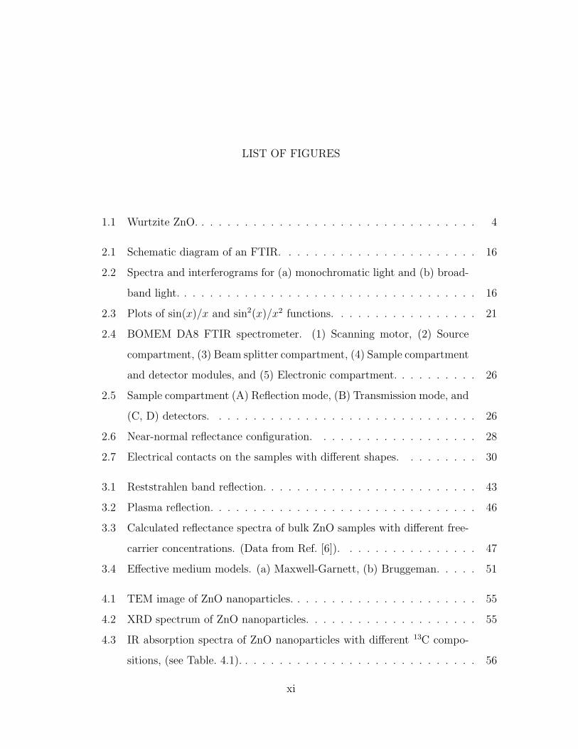
1.1 Wurtzite ZnO. . . . . . . . . . . . . . . . . . . . . . . . . . . . . . . . . 4
2.1 Schematic diagram of an FTIR. . . . . . . . . . . . . . . . . . . . . . . 16
2.2 Spectra and interferograms for (a) monochromatic light and (b) broad-
band light. . . . . . . . . . . . . . . . . . . . . . . . . . . . . . . . . . . 16
2.3 Plots of sin(x)/x and sin2(x)/x2 functions. . . . . . . . . . . . . . . . . 21
2.4 BOMEM DA8 FTIR spectrometer. (1) Scanning motor, (2) Source
compartment, (3) Beam splitter compartment, (4) Sample compartment
and detector modules, and (5) Electronic compartment. . . . . . . . . . 26
2.5 Sample compartment (A) Reflection mode, (B) Transmission mode, and
(C, D) detectors. . . . . . . . . . . . . . . . . . . . . . . . . . . . . . . 26
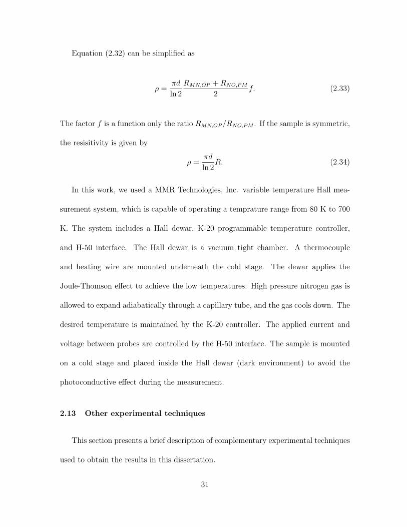
2.6 Near-normal reflectance configuration. . . . . . . . . . . . . . . . . . . 28
2.7 Electrical contacts on the samples with different shapes. . . . . . . . . 30
3.1 Reststrahlen band reflection. . . . . . . . . . . . . . . . . . . . . . . . . 43
3.2 Plasma reflection. . . . . . . . . . . . . . . . . . . . . . . . . . . . . . . 46
3.3 Calculated reflectance spectra of bulk ZnO samples with different free-
carrier concentrations. (Data from Ref. [6]). . . . . . . . . . . . . . . . 47
3.4 Effective medium models. (a) Maxwell-Garnett, (b) Bruggeman. . . . . 51
4.1 TEM image of ZnO nanoparticles. . . . . . . . . . . . . . . . . . . . . . 55
4.2 XRD spectrum of ZnO nanoparticles. . . . . . . . . . . . . . . . . . . . 55
4.3 IR absorption spectra of ZnO nanoparticles with different 13C compo-
sitions, (see Table. 4.1). . . . . . . . . . . . . . . . . . . . . . . . . . . . 56
xi
4.4 IR absorption spectra of zinc acetate precursors with different 13C com-
positions (see Table. 4.1). . . . . . . . . . . . . . . . . . . . . . . . . . 58
4.5 IR absorption spectra of ZnO nanoparticles after each annealing step. . 60
4.6 CO2 and carbonate peak intensities in ZnO nanoparticles after isochronal
annealing. Peaks are normalized to their maxima. . . . . . . . . . . . . 61
4.7 IR absorption spectra of ZnO nanoparticles, (a) prepared in air, (b)
prepared in argon gas. The precursors contain only 13C isotopes [sample
(d)]. . . . . . . . . . . . . . . . . . . . . . . . . . . . . . . . . . . . . . 62
5.1 SIMS results for as-grown, H2 annealed and D2 annealed ZnO nanopar-
ticles. . . . . . . . . . . . . . . . . . . . . . . . . . . . . . . . . . . . . 69
5.2 Infrared reflectance spectra of ZnO nanoparticles. The dotted lines
denote the calculated spectra. . . . . . . . . . . . . . . . . . . . . . . . 72
5.3 Infrared reflectance spectra of hydrogen annealed ZnO nanoparticles
after exposure to air. The dotted lines denote the calculated spectra. . 74
5.4 IR reflectance spectra of hydrogen-annealed sample, under different am-
bients. . . . . . . . . . . . . . . . . . . . . . . . . . . . . . . . . . . . . 75
5.5 Raman spectra of ZnO nanoparticles. . . . . . . . . . . . . . . . . . . . 77
5.6 Free-carrier absorption of ZnO nanoparticles, as-grown and after an-
nealing in hydrogen at 350 C (from Ref. [8]). . . . . . . . . . . . . . . 78
5.7 Infrared absorption spectra of hydrogen annealed ZnO nanoparticles in
KBr matrix (a) 1% wt. and (b) 2% wt. The dotted lines represent the
model. . . . . . . . . . . . . . . . . . . . . . . . . . . . . . . . . . . . . 80
5.8 Conductivity under different ambients. . . . . . . . . . . . . . . . . . . 81
5.9 Conductivity under vacuum and air ambient. . . . . . . . . . . . . . . . 81
5.10 Conductivity under vacuum and nitrogen ambient. . . . . . . . . . . . 82
6.1 Energy states of Cu in ZnO. From Ref. [1] . . . . . . . . . . . . . . . . 87
6.2 IR absorption spectrum of ZnO:Cu nanoparticles at 9 K. . . . . . . . . 90
xii

6.3 IR absorption spectrum of ZnO:Cu nanoparticles at 9 K (3500-3800
cm−1 region) . . . . . . . . . . . . . . . . . . . . . . . . . . . . . . . . . 90
7.1 Fano resonance. . . . . . . . . . . . . . . . . . . . . . . . . . . . . . . . 92
7.2 Fano line shape with different q values. . . . . . . . . . . . . . . . . . . 94
7.3 SEM image of Mg nanorods on a Si substrate. . . . . . . . . . . . . . . 96
7.4 OH and OD absorption peaks on (a) Mg nanorods, (b) Mg powder, and
(c) MgH2 powder. . . . . . . . . . . . . . . . . . . . . . . . . . . . . . . 98
7.5 Gaussian line shape fit of OD absorption peak in the MgH2 sample. . . 99
7.6 Fano line shape fits of OD absorption peaks in (a) Mg nanorods and
(b) Mg powder. . . . . . . . . . . . . . . . . . . . . . . . . . . . . . . . 100
7.7 XRD pattern of Mg powder after reaction with water. . . . . . . . . . . 101
A.1 Linear tri-atomic molecule. . . . . . . . . . . . . . . . . . . . . . . . . . 104
B.1 Schematic diagram of MOCVD system. . . . . . . . . . . . . . . . . . . 107
B.2 XRD diffraction patterns of ZnO films. (a) Undoped ZnO, (b) 1.5 At.
% Mn, (c) 4.5 At. % Mn. Inset: Magnified ZnO (002) scan detecting
slight shift in 2θ positions. . . . . . . . . . . . . . . . . . . . . . . . . . 110
B.3 PIXE spectrum of ZnO:Mn (4.5 At. % Mn) sample. RBS spectrum is
shown in inset. The solid lines represent the modeled spectra. . . . . . 112
B.4 XPS spectra for ZnO and ZnO:Mn films. Zn and O regions. . . . . . . 113
B.5 XPS spectra for ZnO and ZnO:Mn films. Mn regions. . . . . . . . . . . 113
B.6 The ratio of zinc to oxygen compositions as a function of Mn content
calculated from both XPS and PIXE. (a) from PIXE technique, (b) As
recorded XPS surface scan, (c) After Ar+ ion sputtering in XPS and
(d) XPS corrected atomic concentration. . . . . . . . . . . . . . . . . . 115
B.7 Temperature dependent electrical conductivity for undoped as well as
ZnO:Mn films. . . . . . . . . . . . . . . . . . . . . . . . . . . . . . . . . 117
xiii
LIST OF TABLES
1.1 Physical properties of wurtzite ZnO [14] . . . . . . . . . . . . . . . . . 5
2.1 Operating spectral ranges of BOMEM DA8 FTIR components [10]. . . 24
4.1 Isotopic compositions of precursor materials used to synthesize ZnO
nanoparticle samples. . . . . . . . . . . . . . . . . . . . . . . . . . . . . 57
5.1 Parameters used in the calculations. Constants are: ωTO = 410 cm−1,
ωLO = 575 cm−1, and ε∞ = 3.75. . . . . . . . . . . . . . . . . . . . . . . 73
B.1 Growth parameters for un-doped and ZnO:Mn films. . . . . . . . . . . 108
xiv
CHAPTER 1
INTRODUCTION
Control of the electrical and optical properties of nanoparticles is a key require-
ment for practical applications in optoelectronic devices. The control of the number
of free carriers has been achieved by doping the nanoparticles. Doped semiconductors
contain impurities, foreign atoms which are incorporated into the host crystal inten-
tionally or unintentionally. In this work, we investigated impurities in ZnO and Mg
nanostructures.
1.1 Semiconductors at the nanometer scale
As particles approach the nanoscale, they possess two important properties, (1)
the quantum confinement effect [1] and (2) a large ratio of surface area to volume
relative to bulk materials. The large surface area provides numerous atomic sites
for the adsorption of molecules, making the nanoparticles attractive materials for
gas and chemical sensing. Since nanoparticles are small compared to IR and visible
wavelengths, they exhibit characteristic absorption and scattering properties [2]. This
feature has been utilized for materials such as stained glass for many centuries.
1
1.2 Free-carrier concentration
The free-carrier concentration is an important parameter that controls the electrical
properties of a semiconductor. Electronic energy levels in a semiconductor crystal are
separated by a bandgap energy Eg, which is the minimum energy separation between
the conduction band and valence band.
1.2.1 Intrinsic
In a bulk semiconductor, the number of atoms is assumed to be infinite. The
intrinsic free-carrier concentration ni at a given temperature T is given by an Arrhenius
equation [3]:
ni =√
NvNc exp
(
− Eg
2kT
)
, (1.1)
where Eg is the bandgap energy and k is Boltzmann’s constant. The pre-factorsNv and
Nc are the effective density of states of the valence and conduction bands respectively,
and are typically expressed in units of cm−3. In an intrinsic semiconductor, there is
an equal number of electrons and holes.
1.2.2 Doping
Introducing impurity atoms into a semiconductor host leads to an increase in the
free-carrier concentration. In n-type semiconductors, free electrons in the conduction
band are majority charge carriers, whereas holes in the valence band are majority
carriers in p-type semiconductors. Shallow donors and acceptors have a much smaller
2

ionization energy compared to the bandgap energy of the host semiconductor; hence,
they can readily contribute to electrical conductivity.
1.2.3 Free-carrier concentration in semiconductor nanoparticles
In nanoparticles, the number of atoms within a particle is limited (∼ 103 − 105).
Thus, in some cases, the particles contain no free carriers. The properties of a particle
can be changed dramatically when a single dopant is added to or removed from the
particle. Precise control over dopant concentration within each particle is extremely
difficult. Bryan and Gamelin [4] proposed that the dopant distribution among the
nanoparticles can be described by a binomial expression,
P (n|N) =(N)!
n!(N − n)!(xN)n[1 − (xN)]N−n, (1.2)
where n is the number of dopants per nanoparticle. The value N is total number of
sites available for substitution and x is dopant mole fraction.
1.3 Zinc Oxide (ZnO)
Zinc oxide (ZnO) [5,6] is a wide bandgap (3.4 eV at room temperature) semiconduc-
tor that is desirable for many applications. It is attractive for forming various forms of
nanostructures, such as nanorods, nanowires, and nanobelts [7]. Alloying with MgO or
CdO respectively increases or decreases the bandgap energy of ZnO [8]. Transparent
transistors fabricated from ZnO have been reported [9]. With its high exciton bind-
3

ing energy, ZnO is a good candidate for room temperature UV lasers [10]. Its large
piezoelectric constant is promising for ultrasonic tranducers [11]. ZnO is transparent
and electrically conductive, making it an ideal material for solar cell windows [12].
One of the major commercial applications of ZnO is the production of varistors [13].
ZnO varistors have high non-ohmic voltage-current characteristics, which originate
from grain boundaries between ZnO grains. The mineral form of ZnO can be found
in nature and is known as Zincite.
Zinc oxide has the hexagonal wurtzite structure (Fig. 1.1). The crystal can be
described as alternating planes composed of tetrahedrally coordinated O2− and Zn2+
ions, stacked along the c-axis. The physical properties of ZnO semiconductors are
presented in Table 1.1.
FIG. 1.1. Wurtzite ZnO.
4
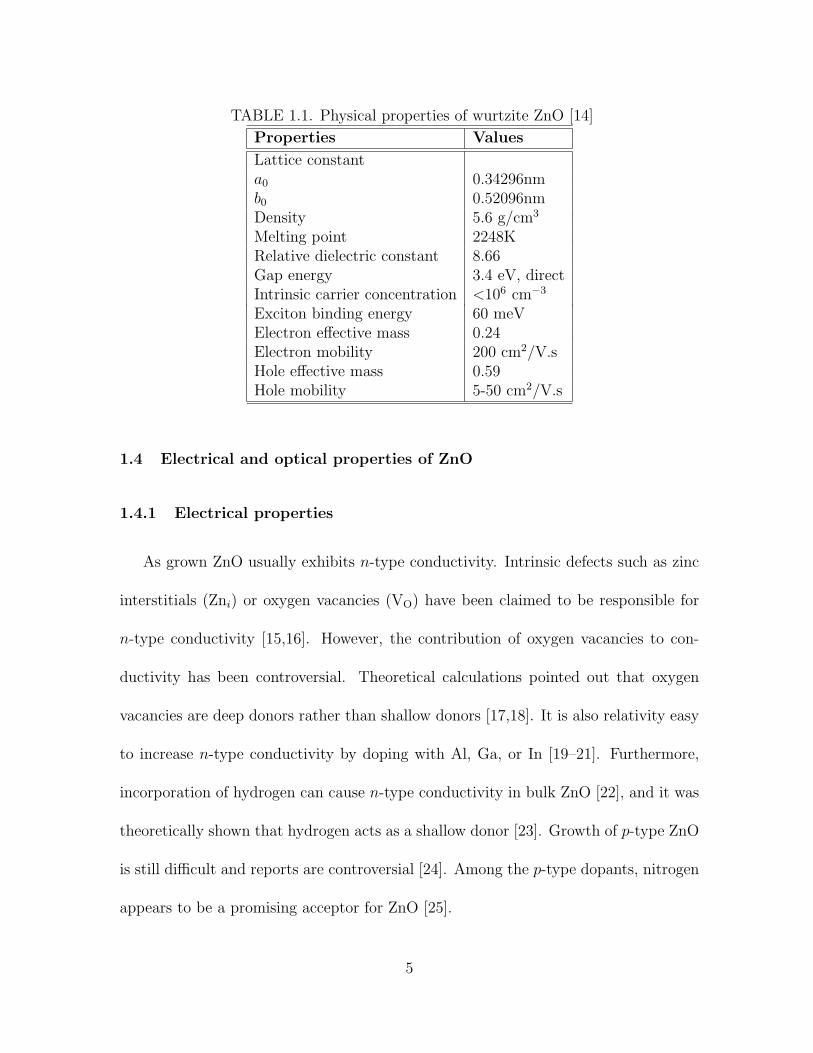
TABLE 1.1. Physical properties of wurtzite ZnO [14]
Properties Values
Lattice constanta0 0.34296nmb0 0.52096nmDensity 5.6 g/cm3
Melting point 2248KRelative dielectric constant 8.66Gap energy 3.4 eV, directIntrinsic carrier concentration <106 cm−3
Exciton binding energy 60 meVElectron effective mass 0.24Electron mobility 200 cm2/V.sHole effective mass 0.59Hole mobility 5-50 cm2/V.s
1.4 Electrical and optical properties of ZnO
1.4.1 Electrical properties
As grown ZnO usually exhibits n-type conductivity. Intrinsic defects such as zinc
interstitials (Zni) or oxygen vacancies (VO) have been claimed to be responsible for
n-type conductivity [15,16]. However, the contribution of oxygen vacancies to con-
ductivity has been controversial. Theoretical calculations pointed out that oxygen
vacancies are deep donors rather than shallow donors [17,18]. It is also relativity easy
to increase n-type conductivity by doping with Al, Ga, or In [19–21]. Furthermore,
incorporation of hydrogen can cause n-type conductivity in bulk ZnO [22], and it was
theoretically shown that hydrogen acts as a shallow donor [23]. Growth of p-type ZnO
is still difficult and reports are controversial [24]. Among the p-type dopants, nitrogen
appears to be a promising acceptor for ZnO [25].
5
The surface properties play an important role in the electrical behavior of ZnO. As
presented by Schmidt et al. [26–28], the electrical conductivity of high resistivity bulk
ZnO is strongly influenced by the sample ambient. The semi-insulating sample can
be transformed into a conductive state under vacuum. They explained this behavior
in terms of a surface conductive channel that exists in vacuum, but is destroyed upon
exposure to air. They proposed that the surface conducting layer is eliminated in air
due to changes in the surface bonds.
1.4.2 Optical properties
The high efficiency of luminescence in the UV to visible regions of the spectrum
makes ZnO an attractive material for optoelectronic applications. The near-bandgap
emission is due to recombinations of free electrons in the conduction band and holes in
the valence band. A broadband emission within the visible region, due to transitions
involving defect states, is a common photoluminescence feature of bulk ZnO [29].
Impurity atoms also contribute to visible emission; e.g., green luminescence from Cu
acceptors in ZnO [30,31].
In the nanoscale, the quantum confinement effect in ZnO nanoparticles was demon-
strated by Shim and Guyot-Sionnest [32,33]. The nanoparticles were made n-type by
electron transfer doping. The nanoparticles exhibited strong mid-IR absorption due
to intraband transitions of electrons in the conduction band (free-carrier absorption).
Since nanoparticles have a large surface area, Dijken et al. [34] investigated the role
of adsorbed oxygen on the emission properties of ZnO nanoparticles. The adsorbed
6

oxygen traps the photogenerated electron and influences the visible emission process.
1.5 Phonons in ZnO
Wurtzite ZnO possesses four atoms per unit cell. Thus, there are 12 phonon
branches (3 acoustic branches and 9 optical branches). The optical phonons at the
Γ-point belong to following irreducible representation,
Γopt = 1A1 + 2B1 + 1E1 + 2E2. (1.3)
The A1 and E1 modes are both Raman and IR active, whereas the E2 mode is only
Raman active. The B1 modes are inactive to both Raman and IR. In the A1 and E1
modes, the atoms oscillate parallel and perpendicular to the c-axis, respectively. The
frequencies of optical phonons range from 98 cm−1 to 591 cm−1 at the Γ-point [35].
1.6 Synthesis of ZnO nanostructures
Zinc oxide nanoparticles have been synthesized by variety of methods. The use of
precursor materials such as zinc acetate, zinc nitrate, or zinc carbonate provides an
efficient way to synthesize the ZnO nanoparticles. The most common method is the
addition of NaOH or LiOH to a zinc acetate solution [36–38]. The overall reaction can
be written as:
Zn(CH3COO)2 + 2 NaOH → ZnO + CH3COONa + H2O. (1.4)
7
In this method, the growth of the particles is governed by temperature, the water
content, and solvents. Growth can be terminated by the addition of organic capping
materials such as alkanes. Solution methods can also be used to grow nanostructured
ZnO such as nanowires. Well-oriented arrays of nanowires were grown on a substrate
under a zinc nitrate aqueous solution [39].
Another method developed by Wang et al. [40] used a pyrolytic reaction to produce
ZnO nanoparticles. In their method, zinc acetate and sodium hydrogen carbonate were
reacted at a certain temperature. They showed that the sizes of the particles can be
controlled by the reaction temperature. The reaction by-product, sodium acetate, acts
as a capping material to prevent further growth of the ZnO nanoparticles. The sodium
acetate was washed away with water after the reaction.
However, a major potential problem is the presence of impurities remaining from
precursor materials and reaction products. Orlijskii et al. [41] reported that Li and Na
impurities act as shallow donors in the ZnO nanoparticles. Hydroxyl (OH) molecules
on the surface play an important role in the luminescence properties of ZnO quantum
dots [42].
1.7 Magnesium: A hydrogen storage material
Hydrogen has potential as an alternative to carbon-based fuels. Using hydrogen
requires a reliable medium for storage and transportation. Among the candidate hy-
drogen storage materials, magnesium compounds have numerous desirable properties.
Magnesium is abundant in nature and it is well known that magnesium hydride (MgH2)
8

can store hydrogen with a concentration as high as 7.6 % wt [43].
1.7.1 Magnesium hydride
Magnesium hydride can be formed by the reaction of magnesium with hydrogen
gas:
Mg + H2 ⇔ MgH2. (1.5)
However, the desorption and absorption processes require moderately high tempera-
tures and long reaction times. The use of magnesium nanostructures may improve
these properties.
1.7.2 Hydrogen production
An alternative application of magnesium and magnesium hydride is to produce
hydrogen from reaction with water [44]. Both Mg and MgH2 react with water and
produce magnesium hydroxide [Mg(OH)2] plus hydrogen:
Mg + H2O → Mg(OH)2 + H2, (1.6)
MgH2 + 2 H2O → Mg(OH)2 + 2 H2. (1.7)
In hydrogen production and storage applications, a major challenging problem is that
the formation of passive layers of Mg(OH)2 and MgO interrupts the further reaction
of magnesium metal, preventing the penetration of hydrogen.
IR absorption and Raman spectroscopy of Mg(OH)2 have been performed previ-
9

ously. Sharp IR absorption peaks were found at 3700 cm−1 and 2721 cm−1 for the
OH and OD stretch modes, respectively [45]. Oliveira and Hase [46] observed slightly
different results, with frequencies at 3698 cm−1 and 2725 cm−1. Other works [47,48]
also reported on OH vibrational modes in Mg(OH)2.
1.8 Outline of the dissertation
Although this work focuses on two different materials, semiconducting ZnO and
metallic Mg, in fact they are related. Introducing Mg atoms into a ZnO host is used to
increase the bandgap of ZnO. Zinc oxide nanostructures are also potential candidates
for hydrogen storage materials [49,50]. The combination of the two materials may
enhance their properties.
Chapter 2 presents a description of the experimental techniques. In Chapter 3,
the theoretical background relevant to this work is discussed. Chapter 4 reports the
presence of CO2 molecules in ZnO nanoparticles, observed by IR spectroscopy. Infrared
reflectance studies on hydrogenated ZnO nanoparticles are discussed in Chapter 5.
The IR optical transition spectra of Cu ions in ZnO nanoparticles are presented in
Chapter 6. In Chapter 7, IR spectroscopy of Mg(OH)2 layers on Mg and MgH2,
formed by reaction with water, is presented.
10

References
[1] Nanoparticles: From Theory to Application, edited by G. Schmid, (Wiley-VCH,
2006).
[2] C. F. Bohren, and D. R. Huffman, Absorption and Scattering of Light by Small
Particles, (Wiley, New York, 1983).
[3] J. S. Blakemore, Semiconductor Statistics, (Dover, New York, 1987).
[4] J. D. Bryan and D. R. Gamelin, Prog. Inorg. Chem. 54, 74 (2005).
[5] W. Hirschwald, P. Bonasewicz, L. Ernst, M. Grade, D. Hofmann, S. Krebs, R.
Littbarski, G. Neumann, M. Grunze, D. Kolb, and H. J. Schulz, Curr. Topics
Mater. Sci. 7, 143 (1981).
[6] U. Ozgur, Ya. I. Alivov, C. Liu, A. Teke, M. A. Reshchikov, S. Dogan, V. Avrutin,
S. J. Cho, and H. Morkoc, J. Appl. Phys. 98, 041301 (2005).
[7] Z. L. Wang, J. Phys. D: Appl. Phys. 16, R829 (2004).
[8] U. Ozgur, and H. Morkoc, in Zinc Oxide Bulk, Thin Films and Nanostructures:
Processing, Properties and Applications, edited by C. Jagadish, and S, Pearton
(Elsevier, Amsterdam, 2006).
[9] J. F. Wager, Science 300, 1245 (2003).
[10] M. H. Huang, S. Mao, H. Feick,H. Yan, Y. Wu, H. Kind, E. Weber, R. Russo,
and P. Yang, Science 292, 1897 (2001).
[11] N. F. Foster, and G. A. Rozgonyi, Appl. Phys. Lett. 8, 221 (1966).
[12] W. Fuhs, in Zinc Oxide-A Material for Micro- and Optoelectronic Applications,
edited by N. H. Nickel and E. Terukov (Springer, Berlin, 2005).
11

[13] K. Eda, IEEE Electrical Insulation Magazine 5, 28 (1989).
[14] S. J. Pearton, D.P. Norton, K. Ip, Y.W. Heo, T. Steiner, Progress in Materials
Science 50, 293 (2005).
[15] E. Harrison, Phys. Rev. 93, 52 (1954).
[16] D. G. Thomas, J. Phys. Chem. Solids 3, 229 (1957).
[17] C. G. Van de Walle, Physica B 308-310, 899 (2000).
[18] A. Janotti, and C. G. Van de Walle, Phys. Rev. B 76 165202 (2007).
[19] S. Y. Myong, S. J. Baik, C. H. Lee, W. Y. Cho, and K. S. Lim, Jpn. J. Appl.
Phys., Part 2 36, L1078 (1997).
[20] B. M. Ataev, A. M. Bagamadova, A. M. Djabrailov, V. V. Mamedov, and R. A.
Rabadanov, Thin Solid Films 260, 19 (1995).
[21] M. Caglar, Y. Caglar, and S. Ilican, Phys. Status Solidi C 4, 1337 (2007).
[22] D. G. Thomas, and J. J. Lander, J. Chem. Phys. 25, 1136 (1956).
[23] C. G. Van de Walle, Phys. Rev. Lett. 85, 1012 (2000).
[24] D. C. Look, and B. Claflin, Phys. Stat. Sol. (b) 241, 624 (2004).
[25] A. Tsukazaki et al., Nat. Mater. 4, 42 (2005).
[26] O. Schmidt, P. Kiesel, C. G. Van de Walle, N. M. Johnson, J. Nause, and G. H.
Dohler, Jpn. J. Appl. Phys. 44, 7271 (2005).
[27] O. Schmidt, A. Geis, P. Kiesel, C. G. Van de Walle, N. M. Johnson, A. Bakin, A.
Waag, and G. H. Dohler, Superlattice and Microstructure 39, 8 (2006).
[28] O. Schmidt, P. Kiesel, D. Ehrentraut, T. Fukuda, and N. M. Johnson, Appl. Phys.
A 88, 71 (2007).
[29] B. K. Meyer, H. Alves, D. M. Hofmann, W. Kriegseis, D. Forster, F. Bertram, J.
Christen, A. Hoffmann, M. StraSSburg, M. Dworzak, U. Haboeck, A. V. Rodina,
Phys. Stat. Sol. (b) 241, 231 (2004).
12

[30] P. Dahan, V. Fleurovy, P. Thurianz, R. Heitzz, A. Hoffmannz, and I. Broserz, J.
Phys. Condens. Matter 10, 2007 (1998).
[31] N. Y. Garces, L. Wang, L. Bai, N. C. Giles, L. E. Halliburton, and G. Cantwell,
Appl. Phys. Lett. 81, 622 (2002).
[32] M. Shim, and P. Guyot-Sionnest, Nature, 407, 981 (2000).
[33] M. Shim, and P. Guyot-Sionnest, J. Am. Chem. Soc, 123, 11651 (2000).
[34] A. van Dijken, E. A. Meulenkamp, D. Vanmaekelbergh, and A. Meijerink, J.
Phys. Chem. B 104, 4355 (2000).
[35] P. Y. Emelie, J. D. Phillips, B. Buller, and U. D. Venkateswaran, J. Electron.
Mater. 35, 525 (2006).
[36] L. Spanhel, and M. A. Ansderson, J. Am. Chem. Soc. 113, 2826 (1991).
[37] E. A. Melenkamp, J. Phys. Chem. B 102, 5566 (1998).
[38] Z. Hu, G. Oskam, and P. C. Searson, J. Colloid Interface Sci. 263, 454 (2003).
[39] L. E. Greene, M. Law, J. Goldberger, F. Kim, J. C. Johnson, Y. Zhang, R. J.
Saykally, and P. Yang, Angew. Chem. Int. Ed. 42, 3031 (2003).
[40] Z. Wang, H. Zhang, L. Zhang, J. Yuan, S. Yan and C. Wang, Nanotechnology
14, 11 (2003).
[41] S. B. Orlinskii, J. Schmidt, P. G. Baranov, D. M. Hofmann, C. M. Donega, and
A. Meijerink, Phys. Rev. Lett. 92, 047603 (2004).
[42] H. Zhou, H. Alves, D. M. Hofmann, B. K. Meyer, G. Kaczmarczyk, A. Hoffmann,
and C. Thomsen, Phys. Status Solidi B 229, 825 (2002).
[43] Hydrogen Energy System: Production and Utilization of Hydrogen and Future,
edited by Y. Yurum, (Springer, 1995).
[44] M. H. Grosjean, M. Zidounce, and L. Rouce, Journal of Alloys and Compounds,
404-406, 712 (2005).
[45] R. A. Buchanan, H. H. Caspers, and J. Murphy, Appl. Opt. 2, 1147 (1963).
[46] E. F. de Oliveira, and Y. Hase, Vibrational Spectroscopy 25, 53 (2001).
13

[47] R. T. Mara, and G. B. B. M. Sutherland, J. Opt. Soc. Am. 43, 1100 (1953).
[48] H. A. Benesi, J. Chem. Phys. 30, 852 (1959).
[49] Q. Wan, C. L. Lin, X. B. Yu, and T. H. Wang, Appl. Phys. Lett. 84, 124 (2004).
[50] H. Pan, J. Luo, H. Sun, Y. Feng, C. Poh, and J. Lin, Nanotechnology, 17, 2963
(2006).
14

CHAPTER 2
EXPERIMENTAL TECHNIQUES
2.1 Fourier transform infrared (FTIR) spectroscopy
The principal experimental method in this work is Fourier transform infrared [1–4]
spectroscopy, which allows us to detect infrared (IR) absorption and reflection prop-
erties over a broad spectral region.
An FTIR is based on a Michelson interferometer, which consists of a beam splitter,
a fixed mirror and a moving mirror (scanning mirror). As shown in Fig. 2.1, light from
the source is separated into two parts and then recombines at the beam splitter after
reflection by the two mirrors. Due to the path difference between the two beams, an
interference pattern is generated. The output beam from interferometer is recorded
as a function of path difference, and is called the interferogram (Fig. 2.2). The IR
spectrum can be obtained by calculating the Fourier transform of the interferogram.
15

FIG. 2.1. Schematic diagram of an FTIR.
Inte
nsity
Frequency
Sig
nal
Path Difference
Inte
nsity
Frequency
(b)
Sig
nal
Path Difference
(a)
FIG. 2.2. Spectra and interferograms for (a) monochromatic light and (b) broadbandlight.
16
2.2 Fourier transform technique
In this section, I will follow the treatment given in Ref. [1]. Mathematically, a
Fourier pair y(x) and E(k) can be represented by:
y(x) =
∫ ∞
−∞
E(k) exp(2πikx)dk, (2.1)
E(k) =
∫ ∞
−∞
y(x) exp(−2πikx)dx. (2.2)
Consider two electromagnetic waves, y1(x) and y2(x), seperated by a path difference
δ:
y1(x) =
∫ ∞
−∞
E(k) exp(2πikx)dk, (2.3)
y2(x) =
∫ ∞
−∞
E(k) exp[2πik(x− δ)]dk. (2.4)
The superposition of two waves results in
y(x) = y1(x) + y2(x) =
∫ ∞
−∞
E(k)[1 + exp(−2πikδ)] exp(2πikx)dk. (2.5)
Let us define the resultant field E(δ, k) as
y(x) =
∫ ∞
−∞
E(δ, k) exp(2πikx)dk. (2.6)
17
By comparing Eq. 2.5 and Eq. 2.6,
E(δ, k) = E(k)[1 + exp(−2πikδ)]. (2.7)
The intensity B(δ, k) is given by
B(δ, k) =1
2cε0E
∗(δ, k)E(δ, k), (2.8)
where ε0 is the permittivity of free space and c is the velocity of light. Plugging in for
E(δ, k) yields
B(δ, k) = cε0E2(k)
[
1 + cos(2πδk)]
. (2.9)
For a broadband source,
I(δ) = cε0
[ ∫ ∞
0
E2(k)dk +
∫ ∞
0
E2(k) cos(2πδk)dk
]
. (2.10)
If the path difference between the two beams is zero (δ = 0), Eq. 2.10 becomes
1
2I(0) = cε0
∫ ∞
0
E2(k)dk. (2.11)
Substituting Eq. 2.11 into Eq. 2.10 yields
[
I(δ) − 1
2I(0)
]
=
∫ ∞
0
cε0E2(k) cos(2πδk)dk. (2.12)
18
Using a Fourier transform, we get
cε0E2(k) =
∫ ∞
0
[I(δ) − I(0)] cos(2πkδ)dδ. (2.13)
The final result is obtained as
B(k) = (constant)
∫ ∞
0
[
I(δ) − 1
2I(0)
]
cos(2πkδ)
dδ. (2.14)
In general form, we can rewrite the above expression as
B(k) =
∫ ∞
−∞
[
I(δ) − 1
2I(0)
]
exp(−2πikδ)dδ. (2.15)
The fast Fourier transform (FFT) method [5] can be used to obtain the spectrum from
the interferogram.
2.3 Apodization
The integration limits in the mathematical forms of the Fourier transform in
Eqs. 2.14 and 2.15 are extended to infinity. However, this is impractical for an FTIR,
since the moving mirror travels only a finite distance. The Fourier transform of a
truncated interferogram results in a spectrum where peaks are surrounded by side
lobes.
If the interferogram is collected between δ − L and δ + L, it is equivalent to
19

multiplying the ideal interferogram by a boxcar function f(x) [6]:
f(x) =
1 | x |≤ L
0 | x |> L.
(2.16)
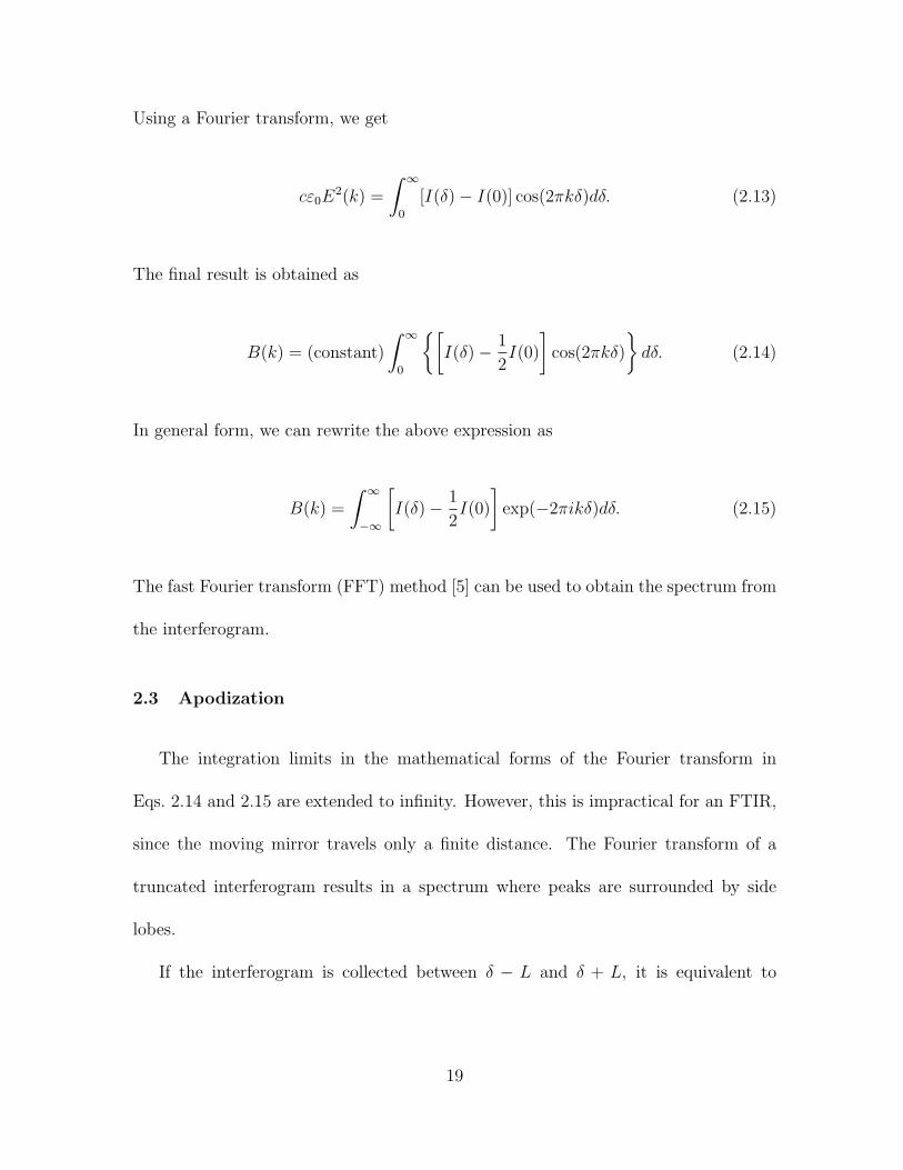
The Fourier transform of boxcar function is a sinc function [sinc(x) = sin(x)/x] (Fig. 2.3).
It can be seen that the convolution of the sinc function introduces a series of positive
and negative side lobes (Fig. 2.3). The side lobes can be suppressed by multiplying
the interferogram with a suitable apodization function such as a Triangular function
prior to performing the FFT:
f(x) =
1 − |x|L
| x |≤ L
0 | x |> L.
(2.17)
The Fourier transform of a triangular function is sinc2(x) = sin2(x)/x2. As shown in
Fig. 2.3, the side lobes are considerably reduced.
Happ-Genzel [7] and Norton-Beer [8] functions are most commonly used for apodiza-
tion.
Happ-Genzel:
f(x) = a+ b cos(xπ
2L
)
. (2.18)
Norton-Beer:
f(x) =k∑
n=0
Cn
[
1 −(x
L
)2]n
;k∑
n=0
Cn = 1. (2.19)
20
-20 -10 0 10 20
-0.2
0.0
0.2
0.4
0.6
0.8
1.0
-20 -10 0 10 20
-0.2
0.0
0.2
0.4
0.6
0.8
1.0
sin(x)/x
sin2(x)/x2
FIG. 2.3. Plots of sin(x)/x and sin2(x)/x2 functions.
2.4 Phase correction
Ideally, the interoferogram should be perfectly symmetrical around zero path dif-
fernce (ZPD). However, in practice, the collected interferogram is somewhat asym-
metrical. This effect is due to a phase shift in incident light that results from optical
components such as the beam splitter, mirrors and recording equipment. The asym-
metric interferograms require a phase correction to obtain the correct spectra. If a
phase error Θ(k) is associated in the asymmetic interferogram, the correlation between
the true spectrum B(k) and measured spectrum will be
B(k) exp[−iΘ(k)] = S(k), (2.20)
21

where S(k) denotes the Fourier transform of the asymmetric interferogram. The phase
error function Θ(k) is given by
Θ(k) = arctan
Im[S(k)]
Re[S(k)]
, (2.21)
For more details on the phase correction method, the reader is referred to Ref. [9].
2.5 Resolution of an FTIR spectrometer
The resolution of an FTIR spectrometer is given by
∆ ∼ 1
δmax
, (2.22)
where ∆ is the resolution in wavenumbers (cm−1) and δmax is maximum path difference,
which is twice the distance of mirror travel distance in centimeters.
2.6 Advantages of an FTIR
There are two primary advantages to using an FTIR spectrometer as compared to
a dispersive spectrometer, Fellgett’s advantage and Jacquinot’s advantage.
Fellgett’s advantage (Multiplex advantage): Generally, the signal-to-noise
ratio (SNR) is proportional to the number of scans or measurement time T (SNR ∝√T ). In a broadband spectrum, the number of spectral elements n between the
frequency range ν1 and ν2 can be defined as n = (ν2 − ν1)/∆ν. In a dispersive
spectrometer, a particular spectral element is recorded in a time t, so that the total
22

time required is T = nt. However, the FTIR spectrometer records information for
all wavelengths in the spectrum simultaneously. During each scan, it records n times
faster than a dispersive spectrometer with the same SNR. If the measurement time is
the same, then the SNR will be increased by factor of√n.
Jacquinot’s advantage (Throughput advantage): In a dispersive spectrom-
eter the energy throughput is limited by the entrance and exit slits of the monochro-
mator. Since the FTIR does not require slits, measurements at higher intensities are
possible. To increase the resolution of a dispersive spectrometer, the slits must be
narrowed. In an FTIR, resolution is increased by increasing mirror travel distance
(section 2.5) with no decrease in energy throughput.
2.7 Spectrometer components and operating frequency range
The operating frequency range of an FTIR depends on three components: the light
source, beam splitter, and detector. The most common type of IR light source is a
high temperature ceramic, which is a black body radiator. The beam splitter consists
of a thin film deposited on a non-absorbing substrate. Ge coated KBr, and Sn2Sb3
coated CaF2 beam splitters are frequently used for the mid-IR region. Far-IR beam
splitters are made of Mylar thin films. Infrared detectors are generally classified into
two types, quantum and thermal. In quantum type detectors such as HgCdTe and
InSb, free electrons excited by IR photons create the electrical signals. The dectector
must be cooled down, typically to liquid nitrogen temperatures, to reduce the ther-
mally excited current. The thermal type, such as the DTGS (Deuterated Tri-Glycine
23

Sulfate) detector, uses the pyroelectric effect. The temperature changes in pyroelec-
tric material, due to absorption of IR photons, causes changes in the polarization and
produces a detectable electric signal. However, the detector response and sensitivity
of thermal type detectors are lower than that of quantum type detectors. The typical
spectral ranges of the different components are summarized in Table 2.1.
TABLE 2.1. Operating spectral ranges of BOMEM DA8 FTIR components [10].
Components Materials Range (cm−1)
Light SourceGlobar 200-10000Quartz 2000-25000
Beam splitterMylar 125-850KBr 450-4000CaF2 1200-8500
DetectorDTGS 10-700
HgCdTe(MCT) 400-5000InSb 1800-14000
2.8 BOMEM DA8 FTIR spectrometer
A BOMEM DA8 FTIR spectrometer (Fig. 2.4) was used in this work. It is versatile
and is capable of attaining 0.02 cm−1 resolution. The upper section of the spectrometer
contains the light source and beam splitter compartment. Light from the source passes
through an aperture (an adjustable mechanical iris) and optical filter before reaching
the beam splitter. The sample compartment and interchangeable detector modules are
located in the middle section (Fig. 2.5). An ellipsoidal mirror is used in the detector
module to focus the light into the detector. A beam switching mirror is situated in
the middle section so that the IR light beam can be directed to the different ports.
24

The lower section contains vacuum leads, preamplifiers and control electronics. The
spectrometer is evacuated by a vacuum pump to minimize the unwanted absorption
of CO2 and H2O molecules from the air. The vacuum also prevents degradation of the
hygroscopic KBr beam splitter. The spectrometer is connected to a computer via an
ethernet cable, and the spectrometer control and data acquisition are performed by
BOMEM PCDA software.
The accurate position of the moving mirror is measured by detecting the interfer-
ence pattern of a He-Ne laser (632 nm), sent through coaxially with the IR beam path
in the interferometer. The precise distance of the scanning mirror travel is obtained by
counting the number of fringes. In addition, a white light source is used to determine
the zero path difference (ZPD) position, since white light produces maximum intensity
at ZPD. A beam splitter for the visible region is mounted at the center of the IR beam
splitter. Dynamic alignment provides accurate alignment of the fixed mirror during
each scan.
2.9 Absorption and transmission
2.9.1 Beer-Lambert law
The relationship between the intensities of the incident (I0) and transmitted (IT )
beam is determined by the Beer-Lambert law,
IT = I0 exp(−αd). (2.23)
25
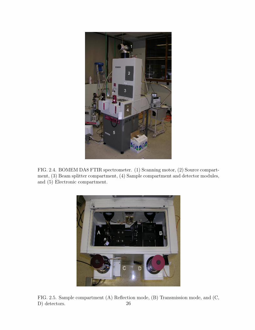
FIG. 2.4. BOMEM DA8 FTIR spectrometer. (1) Scanning motor, (2) Source compart-ment, (3) Beam splitter compartment, (4) Sample compartment and detector modules,and (5) Electronic compartment.
FIG. 2.5. Sample compartment (A) Reflection mode, (B) Transmission mode, and (C,D) detectors. 26

In logarithmic form,
− log
(
ITI0
)
= αd, (2.24)
where α is the absorption coefficient and d is the thickness of the sample.
The transmission T is defined as
T =ITI0. (2.25)
Thus,
log
(
1
T
)
= αd. (2.26)
2.9.2 Integrated absorbance
The integrated absorbance A is defined as
A =
∫
α(ν)dν. (2.27)
The integrated absorbance is useful in cases where the absorption band shape or width
changes with increasing (or decreasing) concentration of the sample.
2.10 Infrared reflectance spectroscopy
In our IR reflectance spectroscopy measurements, the spectra are taken with a
near-normal incidence configuration (Fig. 2.6). The reflectance set-up is built with
two flat mirrors and two concave mirrors. A gold mirror is used as a reference.
27
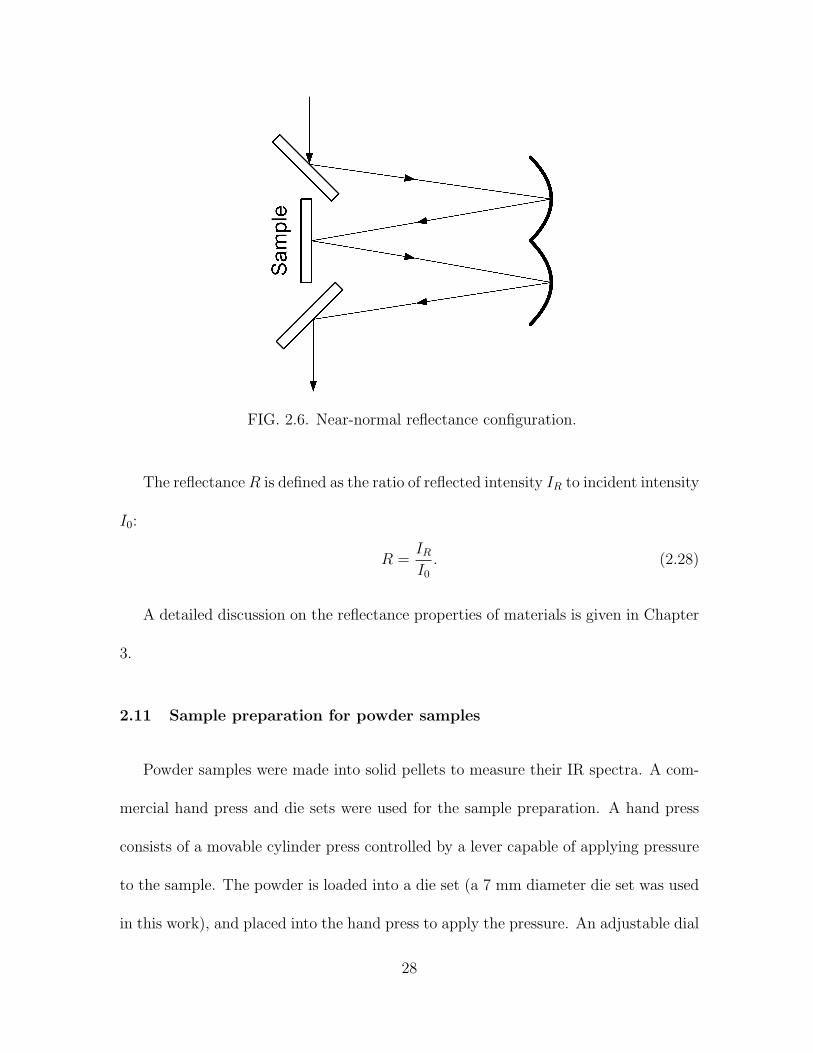
FIG. 2.6. Near-normal reflectance configuration.
The reflectanceR is defined as the ratio of reflected intensity IR to incident intensity
I0:
R =IRI0. (2.28)
A detailed discussion on the reflectance properties of materials is given in Chapter
3.
2.11 Sample preparation for powder samples
Powder samples were made into solid pellets to measure their IR spectra. A com-
mercial hand press and die sets were used for the sample preparation. A hand press
consists of a movable cylinder press controlled by a lever capable of applying pressure
to the sample. The powder is loaded into a die set (a 7 mm diameter die set was used
in this work), and placed into the hand press to apply the pressure. An adjustable dial
28

is used to set the position of the press, and the exerted force can be controlled for the
purpose of reproducibility of the pellets. Some samples are required to be diluted in a
non-absorbing medium such as KBr powder to measure the IR transmission spectrum.
2.12 Electrical measurements
2.12.1 Conductivity
The conductivity σ of a material is determined by its free-carrier concentration n
and mobility µ of the free carriers:
σ = neµ, (2.29)
where e is charge of an electron. The reciprocal of σ is electrical resisitivity ρ = 1/σ.
2.12.2 Van der Pauw method
The 4-probe method in the Van der Pauw geometry [11,12] is a widely used
method to measure the conductivity, carrier concentration and mobility of a sam-
ple. In this method, four small ohmic contacts were placed on the periphery of the
sample (Fig. 2.7). An advantage of the Van der Pauw method is its usefulness for
arbitrarily shaped samples, since the geometric spacing of the contacts is not an issue.
To measure the resistivity, a current iMN was applied into point M and out of point
N , and the potential difference between point P and O was measured. The resistance
RMN,OP is defined as
29

FIG. 2.7. Electrical contacts on the samples with different shapes.
RMN,OP =VP − VO
iMN
. (2.30)
Similarly the resistance RNO,PM is
RNO,PM =VM − VP
iNO
. (2.31)
More precise results can be achieved by taking several measurements in forward and
reverse polarities, and averaging.
Van der Pauw showed that the resisitivity ρ is determined by
exp
(
− πd
ρRMN,OP
)
+ exp
(
− πd
ρRNO,PM
)
= 1, (2.32)
where d is the thickness of the sample.
30
Equation (2.32) can be simplified as
ρ =πd
ln 2
RMN,OP +RNO,PM
2f. (2.33)
The factor f is a function only the ratio RMN,OP/RNO,PM . If the sample is symmetric,
the resisitivity is given by
ρ =πd
ln 2R. (2.34)
In this work, we used a MMR Technologies, Inc. variable temperature Hall mea-
surement system, which is capable of operating a temprature range from 80 K to 700
K. The system includes a Hall dewar, K-20 programmable temperature controller,
and H-50 interface. The Hall dewar is a vacuum tight chamber. A thermocouple
and heating wire are mounted underneath the cold stage. The dewar applies the
Joule-Thomson effect to achieve the low temperatures. High pressure nitrogen gas is
allowed to expand adiabatically through a capillary tube, and the gas cools down. The
desired temperature is maintained by the K-20 controller. The applied current and
voltage between probes are controlled by the H-50 interface. The sample is mounted
on a cold stage and placed inside the Hall dewar (dark environment) to avoid the
photoconductive effect during the measurement.
2.13 Other experimental techniques
This section presents a brief description of complementary experimental techniques
used to obtain the results in this dissertation.
31
2.13.1 Raman spectroscopy
Raman spectroscopy is based on inelastic scattering of light by materials. When a
beam of photons interacts with the material, the vast majority of photons are scattered
with unchanged energy. This scattering process is known as Rayleigh scattering. Only
a small portion of photons are scattered with a energy shift. The energy difference
between incident and scattered photons is equal to the vibrational energy of atoms
inside the crystal and is called a Raman shift. The Raman process can be explained
with a classical treatment [13].
The polarization P of a material is related to the polarizability α and incident
electric field E = E0 cos(ω0t),
P = αE0 cos(ω0t). (2.35)
The normal mode vibration of the atoms with a frequency ωv is
u = u0 cos(ωvt). (2.36)
We can expand α in a Taylor series with respect to normal mode coordinate,
α = α0 +
(
∂α
∂u
)
u+ · · · (2.37)
32
Combining Eqs. 2.35-2.37,
P = α0E0 cos(ω0t) +
(
∂α
∂u
)
u0E0 cos(ωvt) cos(ω0t) + · · · (2.38)
The first term of Eq. 2.38 represents Rayleigh scattering, and the second term describes
Raman scattering. Using a trigonometric identity we can rewrite the second term as,
(
∂α
∂u
)
u0E0 cos(ωvt) cos(ω0t) =1
2
(
∂α
∂u
)
u0E0cos[(ω0 − ωv)t] + cos[(ω0 + ωv)t].
(2.39)
The Raman scattered photons are therefore detected at two frequencies, (ω0 − ωv)
and (ω0 + ωv). The frequencies are known as the Stokes and anti-Stokes frequencies,
respectively. Since the Raman process is a weak effect, an intense light source is
required in the measurement system to achieve a reliable intensity of scattered photons.
A typical Raman system consists of 3 main components: (a) laser excitation source,
(b) monochromator, and (c) detector. The laser beam is focused onto the sample and
scattered photons are detected with the monochromator and detector.
Raman spectra were taken with a cw-Kimmon laser (He-Cd laser with a 325
nm wavelength) and JY-Horiba micro-Raman/PL system located at Department of
Physics, University of Idaho (Prof. Leah Bergman).
33

2.13.2 Transmission electron microscopy (TEM)
In a conventional light microscope, the image resolution is limited by the Rayleigh
criterion [14],
δ =0.61λ
µ sin β, (2.40)
where µ is refractive index of the viewing medium, and β is semi-angle of collection
of the magnifying lens. However, a TEM uses electrons instead of photons, and the
wavelength λ of electrons is much shorter than that of visible light. Therefore a
high resolution image can be obtained. Electrons produced by an electron gun are
accelerated by a high voltage electrode and then focused into a small beam by using
electromagnetic condenser lenses. A phosphor screen is placed behind the sample, and
transmitted electrons are projected onto the screen as an image. The images can be
taken in either bright-field mode or dark-field mode. In a bright-field image, only the
direct transmitted beam is collected, while the scattered electrons are collected in a
dark-field image.
For sample preparation, the nanoparticles were suspended in ethanol and the sol-
vent was dropped onto a copper grid. The TEM images were taken by Prof. Grant
Norton’s group at WSU. A Philips CM200 Transmission Electron Microscope was
used.
34

2.13.3 X-ray diffraction (XRD)
Each crystalline solid has a unique XRD pattern to identify its crystal structure.
When X-ray light with a wavelength λ is incident on a crystal, a diffraction peak
occurs if the Bragg condition is satisfied:
nλ = 2d sin θ, (2.41)
where d is the lattice spacing of the crystal and θ is the angle of incidence. The Cu
Kα emission (λ = 1.5418 A) from a copper target is the most common X-ray source
for the diffraction measurement. Furthermore, a powder XRD pattern is also used to
determine the average size of the nanoparticles. The particle size L can be calculated
by using the Scherrer formula:
L =0.9λ
∆ cos θ, (2.42)
where λ is the wavelength of the X-ray, and ∆ is width (in radians) of the peak at 2θ.
The XRD measurements were performed at the GeoAnalytical Laboratory, WSU,
with a Siemens D-500 X-ray powder diffractometer. The powder sample was smeared
onto a quartz slide with an organic solvent such as ethanol or acetone to measure the
diffraction pattern.
35
References
[1] R. J. Bell, Introductory Fourier Transform Spectroscopy (Academic Press, New
York, 1972).
[2] P. R. Griffiths and J. A. de Haseth, Fourier Transform Infrared Spectrometry
(Wiley, New York, 1986).
[3] J. B. Bates, Science 191, 31 (1976).
[4] W. D. Perkins, J. Chem. Educ. 63, A5 (1986).
[5] J. W. Cooley and J. W. Turkey, Math. Computat. 19, 297 (1965).
[6] J. F. Rabolt and R. Bellar, Appl. Spectroscopy 35, 132 (1981).
[7] H. Happ and L. Genzel, Infrared Phys. 1, 39 (1961).
[8] R. H. Norton and R. Beer, J. Opt. Soc. Am. 66, 259 (1976).
[9] M. L. Forman, W. H. Steel and G. A. Vanasse, J. Opt. Soc. Am. 56, 59 (1966).
[10] The DA8 Series FT-IR Spectrometer Catalog (Bomem Inc., Quebec).
[11] L. J. van der Pauw, Philips Res. Rept. 13, 1 (1958).
[12] L. J. van der Pauw, Philips Tech. Rev. 20, 220 (1958).
[13] A. Schulte, and Y. Guo, in Handbook of Applied Solid State Spectroscopy, edited
by D. R. Vij (Springer, New York, 2006).
[14] P. E. J. Flewitt, and R. K. Wild, Physical Methods for Materials Characterisation
(Institute of Physics Publishing, 1994).
36
CHAPTER 3
THEORY
The purpose of this chapter is to present the theory and relevant equations for the
work in Chapter 5.
3.1 Reflectivity and Fresnel’s equation
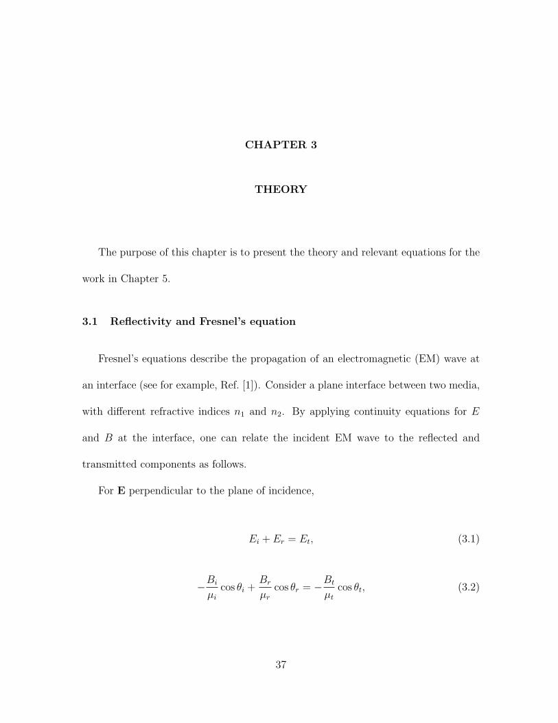
Fresnel’s equations describe the propagation of an electromagnetic (EM) wave at
an interface (see for example, Ref. [1]). Consider a plane interface between two media,
with different refractive indices n1 and n2. By applying continuity equations for E
and B at the interface, one can relate the incident EM wave to the reflected and
transmitted components as follows.
For E perpendicular to the plane of incidence,
Ei + Er = Et, (3.1)
−Bi
µi
cos θi +Br
µr
cos θr = −Bt
µt
cos θt, (3.2)
37
for E parallel to the plane of incidence,
Bi
µi
+Br
µr
=Bt
µt
, (3.3)
Ei cos θi − Er cos θr = Et cos θt. (3.4)
The subscripts i, r and t denote incidence, reflected and transmitted, respectively.
Relating the magnetic fields to the electric fields, and using the above equations,
the reflection coefficients are given by Fresnel’s equations:
r⊥ =
(
Er
Ei
)
⊥
=n1 cos θi − n2 cos θi
n1 cos θi + n2 cos θt
,
r‖ =
(
Er
Ei
)
‖
=n2 cos θi − n1 cos θt
n1 cos θt + n2 cos θi
.
(3.5)
The simplest form of Eq. 3.5 occurs at normal incidence, θi = θr = θt = 0, in
which case the reflectance R is
R = |r|2 =
∣
∣
∣
∣
n2 − n1
n2 + n1
∣
∣
∣
∣
2
. (3.6)
If we consider the interface between vacuum (n1 = 1) and a medium with n2 =√ǫ,
we can rewrite Eq. 3.6 as
R =
∣
∣
∣
∣
√ε− 1√ε+ 1
∣
∣
∣
∣
2
, (3.7)
or
R =(n− 1)2 + κ2
(n+ 1)2 + κ2, (3.8)
38

where ε, n and κ are dielectric function, real and imaginary parts of the refractive
index, respectively. The dielectric function is a complex number and frequency depen-
dent.
3.2 Dielectric function
The dielectric function ε(ω) describes the linear response of a material to an applied
electric field. Valence electrons, phonons and free carriers contribute to the dielectric
properties of a material. The valence electrons’ contribution to the dielectric function
is essentially constant (ε∞), and is known as the high frequency dielectric constant.
Response to light in the IR region is dominated by contributions from phonons and
free carriers.
In a presence of an applied electric field E, atoms in the material become polarized.
The induced polarization P is proportional to the applied electric field E [2]:
P = ǫ0χE, (3.9)
where χ is the electric susceptibility of the medium. However, from the definition of
the electric displacement D,
D = ǫ0E + P = ǫ0(1 + χ)E = ǫ0εE. (3.10)
39
We can therefore define the dielectric constant ε as
ε = 1 + χ. (3.11)
3.2.1 Lattice vibration contribution
In a crystal, the atoms are bound to their equilibrium positions. When the atoms
move from equilibrium, they oscillate at characteristic frequencies, due to a restoring
force. These vibrations are so called phonon [3] modes of the crystal, and have reso-
nant frequencies in the infrared region. There are two types of phonons, longitudinal
and transverse. For longitudinal phonons, the displacements of the atoms coincide
with the direction of propagation of the wave. For transverse phonons, atoms move
perpendicular to the wave propagation. If the crystal has more than one atom in
the unit cell, the vibrations of the atoms develop two modes, namely acoustic and
optical phonon modes. In a optical phonon mode, any two neighboring atoms os-
cillate around their equilibrium positions, out of phase with respect to each other.
Transverse electromagnetic waves can only couple to transverse optical (TO) modes.
However, longitudinal optical phonons (LO) also play an important role in the infrared
properties of materials.
Starting from the damped harmonic oscillator equation with resonance frequency
ωTO [4]:
µd2x
dt2+ µΓ
dx
dt+ µω2
TOx = eE0 exp(−iωt), (3.12)
where µ and Γ are the reduced mass and damping factor of the TO phonon, respec-
40
tively. The solution of Eq. 3.12 is x = x(0) exp(iωt), with
x(0) =eE0
µ(ω2TO − ω2 − iΓω)
. (3.13)
For a material with N ion pairs with of effective charge e, the polarization P is given
by
P =Ne2E0
µ(ω2TO − ω2 − iΓω)
. (3.14)
We can combine Eqs. 3.9 and 3.14 to obtain
ε(ω) = 1 + χ+Ne2
µǫ0
1
(ω2TO − ω2 − iΓω)
. (3.15)
The term χ in Eq. 3.15 represents a non-resonant background. In the limits of low
and high frequency, we obtain from above equation
ε(0) = ε0 = 1 + χ+Ne2
µǫ0
1
ω2TO
, (3.16)
and
ε(∞) = ε∞ = 1 + χ. (3.17)
Substituting Eqs. 3.16 and 3.17 into Eq. 3.15, we get
ε(ω) = ε∞ + (ε0 − ε∞)ω2
TO
(ω2TO − ω2 − iΓω)
. (3.18)
41

However, the ratio of ε0 to ε∞ is given by the Lyddane-Sachs-Teller (LST) relation [5]
ω2LO
ω2TO
=ε0
ε∞. (3.19)
Thus, Eq. 3.18 becomes
ε(ω) = ε∞
[
1 +ω2
LO − ω2TO
ω2TO − ω2 − iΓω
]
. (3.20)
For a small damping factor Γ = 0, we can rewrite the above expression as
ε(ω) = ε∞
[
1 +ω2
LO − ω2TO
ω2TO − ω2
]
. (3.21)
From Eq. 3.21, it can be seen that between the ωLO and ωTO frequencies, ε(ω) is
negative; thus, the refractive index is imaginary. The reflectivity is therefore 1 between
the ωLO and ωTO. The strong reflection of infrared radiation between the optical
phonon frequencies is known as reststrahlen (residual rays) band reflection. A plot of
Eq. 3.20 is shown in Fig. 3.1. In non-polar crystals such as Si or Ge, reststrahlen
band reflection is absent, since ωLO = ωTO.
3.2.2 Free carrier contribution
The doping of a semiconductor leads to an increase in free-carrier concentration.
The response of a free carrier to an applied electric field can be described by a classical
Drude model. Free electrons are different from bound electrons since the restoration
42

0.0
0.2
0.4
0.6
0.8
1.0
Ref
lect
ivity
Wavenumbers
LOTO
FIG. 3.1. Reststrahlen band reflection.
43
force on the free electron is zero. The motion of a free electron in external electric
field E0 exp(−iωt) can be modeled by a single harmonic oscillator with a resonance
frequency ω0 = 0:
md2x
dt2+mγ
dx
dt= eE0 exp(−iωt), (3.22)
where m and γ are the mass and damping factor of the electron, respectively. The
solution of the above differential equation leads to
x(t) = − e
m
1
(ω2 + iγω)E0 exp(−iωt). (3.23)
Since each electron contributes a dipole moment ex(t), the polarization of a medium
with a free-electron density n is
P = nex(t) = −Ne2
m
1
(ω2 + iγω)E0 exp(−iωt). (3.24)
Using a similar derivation as in section 3.2.1, the dielectric function ε(ω) can be derived
as
ε(ω) = 1 −ω2
p
(ω2 + iγω), (3.25)
where ωp is the so-called plasma frequency,
ωp =
√
ne2
ε0m. (3.26)
44
For a small damping factor γ = 0, we can simplify the above expression as
ε(ω) = 1 −ω2
p
ω2. (3.27)
For frequencies below the plasma frequency, the dielectric constant is negative and
the refractive index is purely imaginary. In this region, reflectivity is nearly one, and
no electromagnetic wave can propagate into the medium, as evident in most metallic
mirrors. This reflection is called plasma reflection. Above the plasma frequency, where
the refractive index is real, the electromagnetic waves propagate into the medium and
the dielectric function approaches unity at high frequency. Plasma reflection can be
seen in both metals and doped semiconductors. A plot of Eq. 3.25 is shown in Fig. 3.2.
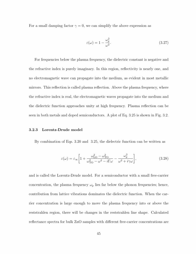
3.2.3 Lorentz-Drude model
By combination of Eqs. 3.20 and 3.25, the dielectric function can be written as
ε(ω) = ε∞
[
1 +ω2
LO − ω2TO
ω2TO − ω2 − iΓω
−ω2
p
ω2 + iγω
]
, (3.28)
and is called the Lorentz-Drude model. For a semiconductor with a small free-carrier
concentration, the plasma frequency ωp lies far below the phonon frequencies; hence,
contribution from lattice vibrations dominates the dielectric function. When the car-
rier concentration is large enough to move the plasma frequency into or above the
reststrahlen region, there will be changes in the reststrahlen line shape. Calculated
reflectance spectra for bulk ZnO samples with different free-carrier concentrations are
45

0.0
0.5
1.0
p
Ref
lect
ivity
Wavenumbers
FIG. 3.2. Plasma reflection.
presented in Fig. 3.3. It can be seen that, the high free-carrier concentration in heavily
doped sample dominates the reflectivity, with only a weak reststrahlen band reflection.
3.3 Surface roughness scattering
The theory described in section 3.1 is based on an ideally smooth surface. However,
in practice, we need to consider effect of surface roughness. Due to surface roughness,
the reflectance beam can be divided into a specular component and scattering com-
ponent (Rtot = Rspec + Rdiffuse). The relationship between the total reflectance and
46

200 400 600 800 1000 12000.0
0.2
0.4
0.6
0.8
1.0
R
efle
ctan
ce
Wavenumbers (cm-1)
n=9.3x10¹⁶
n=4.2x10¹⁸
n=5.0x10¹⁹
FIG. 3.3. Calculated reflectance spectra of bulk ZnO samples with different free-carrierconcentrations. (Data from Ref. [6]).
specular reflectance component is given by [7]
Rspec
Rtot
= exp
(
−4πδ cos θ
λ
)2
, (3.29)
where δ is the rms value of the surface roughness.
47
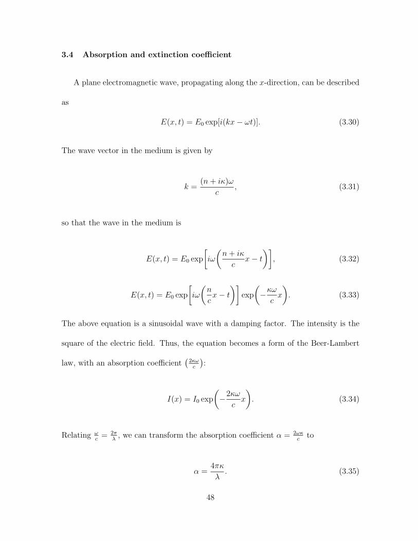
3.4 Absorption and extinction coefficient
A plane electromagnetic wave, propagating along the x-direction, can be described
as
E(x, t) = E0 exp[i(kx− ωt)]. (3.30)
The wave vector in the medium is given by
k =(n+ iκ)ω
c, (3.31)
so that the wave in the medium is
E(x, t) = E0 exp
[
iω
(
n+ iκ
cx− t
)]
, (3.32)
E(x, t) = E0 exp
[
iω
(
n
cx− t
)]
exp
(
−κωcx
)
. (3.33)
The above equation is a sinusoidal wave with a damping factor. The intensity is the
square of the electric field. Thus, the equation becomes a form of the Beer-Lambert
law, with an absorption coefficient(
2κωc
)
:
I(x) = I0 exp
(
−2κω
cx
)
. (3.34)
Relating ωc
= 2πλ
, we can transform the absorption coefficient α = 2ωκc
to
α =4πκ
λ. (3.35)
48

The absorption coefficient α is related to imaginary part of refractive index, which is
also called the extinction coefficeint.
3.5 Effective medium approximation (EMA)
When the wavelength of the incident electromagnetic wave is much greater than
the particle sizes of the inhomogeneous composite material, the material can be treated
as a homogeneous material or an effective medium [8]. EMA is a method developed
to predict the optical and dielectric properties of a composite as a function of each
constituent material, and their volume fractions.
The Clausius-Mossotti relation gives a connection between the macroscopic dielec-
tric function ε and microscopic polarizibility α:
ε− 1
ε+ 2=
1
3ε0
∑
j
njαj, (3.36)
where nj is concentration (per unit volume) of the jth component, and the polarizibility
of a spherical particle with dielectric function εj, and radius r is given by
α = 4πε0r3
(
εj − 1
εj + 2
)
. (3.37)
Combining Eqs. 3.36 and 3.37, we can write
εeff − 1
εeff + 2=∑
j
fj
εj − 1
εj + 2. (3.38)
49

The parameter fj is the volume fraction of the jth component, and∑
j fj = 1. The
above equation is called the Lorentz-Lorenz effective medium expression.
If we consider a host dielectric function εh, instead of vacuum, then Eq. 3.38 can
be rewritten in the general form:
εeff − εh
εeff + 2εh
=∑
j
fj
εj − εh
εj + 2εh
. (3.39)
Based on the above equation, different models have been developed by choosing
different host materials. For a composite material, a mixture of materials A and B,
the Maxwell-Garnett model [9] assumes that one material acts as the host. Choosing
A as the host material (ǫh = ǫA), Eq. 3.39 is simplified to
εeff − ǫAεeff + 2εA
= fB
εB − εA
εB + 2εA
. (3.40)
The Maxwell-Garnett model has been successfully applied to explain the optical re-
sponse of metal-doped stained glasses [11]. However, the model is expected to be
satisfactory only in the case of low concentration, in which case the host material and
inclusions are not interchangeable.
In some cases, if the volume fractions fj are comparable to each other, it is unclear
how to choose the host material. To solve this quandary, Bruggeman [10] proposed
that neither component should play the host role. All materials are considered to be
embedded in the effective medium itself, which is equivalent to εeff = εh:
50

∑
j
fj
εj − εeff
εj + 2εeff
= 0. (3.41)
The Maxwell-Garnett (MG) model and Bruggeman (BR) model are the most com-
monly used models. The difference between the two models is that MG describes
inclusions B completely surrounded by the host A, whereas the BR model refers to
an aggregate or random mixture where all components are inserted into the effective
medium itself (Fig. 3.4).
FIG. 3.4. Effective medium models. (a) Maxwell-Garnett, (b) Bruggeman.
51
References
[1] E. Hecht, Optics, 4th Ed. (Addison Wesley, San Francisco, 2002).
[2] J. D. Jackson, Classical Electrodynamics, 3rd Ed. (Wiley, New York, 1999).
[3] C. Kittel, Introduction to Solid State Physics, 7th Ed. (Wiley, New York, 1996).
[4] P. Y. Yu, and M. Cardona, Fundamentals of Semiconductors, (Springer-Verlag,
Berlin, 1996)
[5] R. H. Lyddane, R. Sachs, and E. Teller, Phys. Rev. 59, 673 (1941).
[6] E. F. Venger, A. V. Melnichuk, L. Y. Melnichuk and Y. A. Pasechnik, Phys. Stat.
Sol. (b) 188, 823 (1995).
[7] T. V. Vorburger, E. Marx and T. R. Lettieri, Appl. Optics 32, 3401 (1993).
[8] D. E. Aspnes, Thin Solid Films, 89, 249 (1982).
[9] J. C. M. Garnett, Phils. Trans. R. Soc. London 203, 385 (1904).
[10] D. A. G. Bruggeman, Ann. Phys. (Leipzig) 24, 636 (1935).
[11] T. Unga, L. M. Liz-Marzanb and P. Mulvaney, Colloids and Surfaces A 202, 119
(2002).
52
CHAPTER 4
CARBON DIOXIDE IMPURITIES IN ZINC OXIDE
NANOPARTICLES
In this chapter, we report the presence of CO2 molecules in ZnO nanoparticles,
observed by infrared (IR) spectroscopy. Our results revealed that the CO2 impurities
are formed by reactions involving the organic precursors.
4.1 Synthesis of ZnO nanoparticles
The synthesis method described in Ref. [1] was used in this work. Zinc acetate
dihydrate [Zn(CH3COO)2 · 2H2O] and sodium hydrogen carbonate (NaHCO3) were
mixed thoroughly at room temperature, with a molar ratio of 1:2.4. The mixture was
sealed in an evacuated quartz ampoule filled with 2/3 atm argon gas. In this way,
we could prevent contamination from ambient air during the reaction. The reaction
was performed at 200 C for 3 hours. After the reaction process, the product was
washed several times with distilled water to remove the by-product sodium acetate
(CH3COONa), and dried at room temperature overnight. The powder was pressed
Portions of this chapter were published as: W. M. Hlaing Oo, M. D. McCluskey, A. D. Lalonde,and M. G. Norton, “Infrared spectroscopy of ZnO nanoparticles containing CO
2impurities.” Appl.
Phys. Lett. 86, 073111 (2005).
53
into a thin pellet (thickness 0.25 mm) and then annealed in argon at 350 C for 2
hours to remove the remaining water.
A transmission electron microscope (TEM) image of the ZnO particles is shown in
Fig. 4.1. The particles were roughly spherical, with a size of about 20 nm. The crystal
structure was examined by powder X-ray diffraction (XRD) analysis. Three dominant
peaks in the (XRD) spectrum (Fig. 4.1) confirmed the hexagonal wurtzite structure,
in agreement with previous work [1].
4.2 Vibrations of CO2
molecules
Room temperature IR absorption spectra were obtained with a Bomem DA8 vac-
uum Fourier transform infrared (FTIR) spectrometer with a liquid nitrogen cooled
HgCdTe detector. The instrumental resolution was 4 cm−1, and the spectra were av-
eraged over 500 scans. As shown in Fig. 4.3 (spectrum a), a strong IR absorption peak
was observed at a frequency of 2342 cm−1. In addition, a weak absorption peak was
observed at 2277 cm−1. These peaks are assigned to asymmetric stretch frequencies
(ν3) of 12CO2 and 13CO2 molecules, respectively. For a linear free CO2 molecule, the
ν3 vibrational frequency is estimated by (APPENDIX A)
ν =
√
κ
(
2
MC
+1
MO
)
, (4.1)
where MC and MO are the masses of carbon and oxygen respectively, and κ is an
effective spring constant. The calculated frequency ratio of ν(12CO2) to ν(13CO2)
54

FIG. 4.1. TEM image of ZnO nanoparticles.
30 32 34 36 38 400
100
200
300
400
500
(101
)
(002
)
Inte
nsity
(arb. u
nits
)
2 Theta
(100
)
FIG. 4.2. XRD spectrum of ZnO nanoparticles.
55

is 1.029, in good agreement with the observed ratio of 1.028. The ratio of peak
intensities is in agreement with the natural isotopic abundance ([13C]/[12C]=0.01).
Broad absorption peaks in the region between 1200 cm−1 and 1700 cm−1 were also
observed. Those absorption bands are due to vibrations of carbonates (ZnCO3) [2].
2200 2250 2300 2350 2400
(b)
Wavenumbers (cm-1)
(a)
(c)
Abs
orba
nce
(arb. u
nits
)
(d)
FIG. 4.3. IR absorption spectra of ZnO nanoparticles with different 13C compositions,(see Table. 4.1).
56
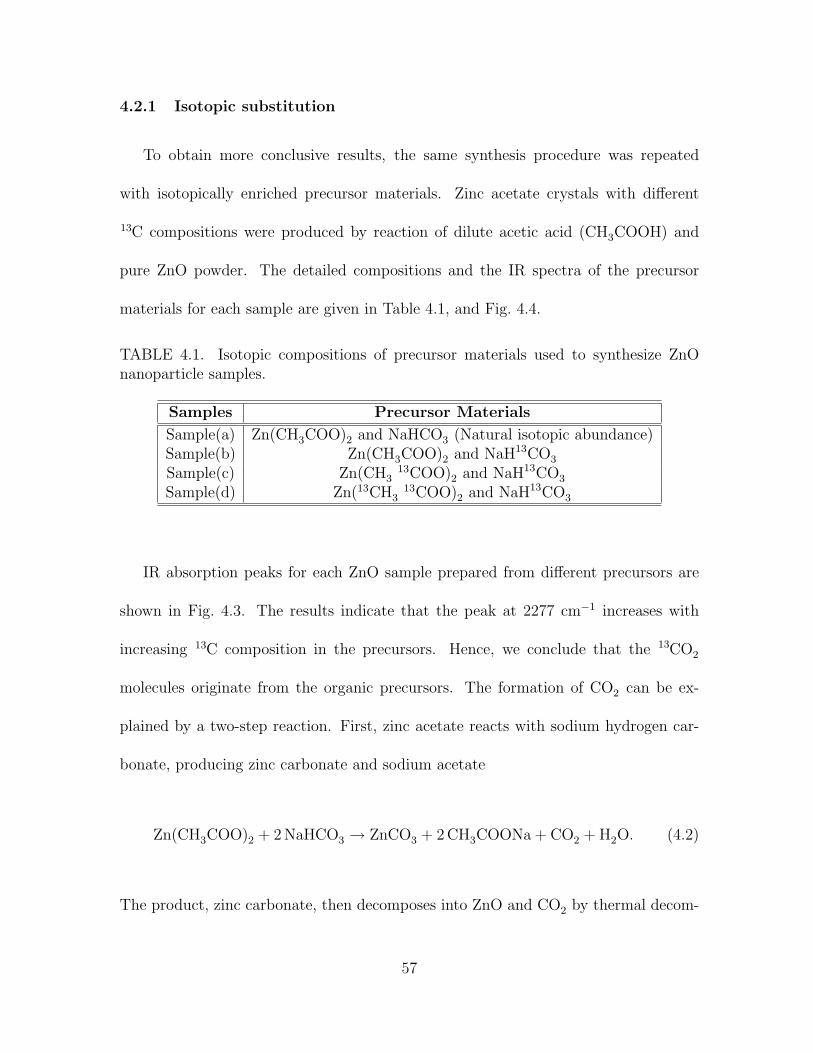
4.2.1 Isotopic substitution
To obtain more conclusive results, the same synthesis procedure was repeated
with isotopically enriched precursor materials. Zinc acetate crystals with different
13C compositions were produced by reaction of dilute acetic acid (CH3COOH) and
pure ZnO powder. The detailed compositions and the IR spectra of the precursor
materials for each sample are given in Table 4.1, and Fig. 4.4.
TABLE 4.1. Isotopic compositions of precursor materials used to synthesize ZnOnanoparticle samples.
Samples Precursor Materials
Sample(a) Zn(CH3COO)2 and NaHCO3 (Natural isotopic abundance)Sample(b) Zn(CH3COO)2 and NaH13CO3
Sample(c) Zn(CH313COO)2 and NaH13CO3
Sample(d) Zn(13CH313COO)2 and NaH13CO3
IR absorption peaks for each ZnO sample prepared from different precursors are
shown in Fig. 4.3. The results indicate that the peak at 2277 cm−1 increases with
increasing 13C composition in the precursors. Hence, we conclude that the 13CO2
molecules originate from the organic precursors. The formation of CO2 can be ex-
plained by a two-step reaction. First, zinc acetate reacts with sodium hydrogen car-
bonate, producing zinc carbonate and sodium acetate
Zn(CH3COO)2 + 2 NaHCO3 → ZnCO3 + 2 CH3COONa + CO2 + H2O. (4.2)
The product, zinc carbonate, then decomposes into ZnO and CO2 by thermal decom-
57
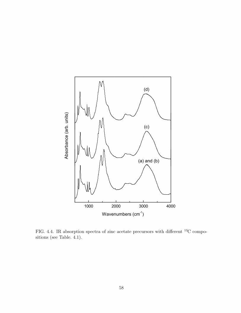
1000 2000 3000 4000
Wavenumbers (cm-1)
(a) and (b)
(c)
Abs
orba
nce
(arb. u
nits
)
(d)
FIG. 4.4. IR absorption spectra of zinc acetate precursors with different 13C compo-sitions (see Table. 4.1).
58

position
ZnCO3 → ZnO + CO2. (4.3)
These reactions account for the observed IR absorption peaks of the carbonates, which
remain in the samples (Fig. 4.5). Since zinc carbonate is insoluble in water, one cannot
simply remove unreacted zinc carbonate by washing with water. The zinc carbonate
therefore remains in the sample and acts as a source of CO2.
4.3 Stability of CO2
molecules
To further investigate the stability of CO2 in nanoparticles, isochronal annealing
experiments were performed. The annealing process was carried out in an open-air
furnace, over a temperature range of 200 C to 700 C. Samples (with natural isotopic
abundance) were annealed for a duration of 1 hour at each temperature. IR spectra
were taken after each annealing step.
As shown in Figs. 4.5 and 4.6, the intensity of the CO2 vibrational peak increases
with increasing temperature. Correspondingly, the carbonate peaks decrease upon
annealing. These observations are in agreement with our model assumption that zinc
carbonate is a source of CO2 impurities.
59
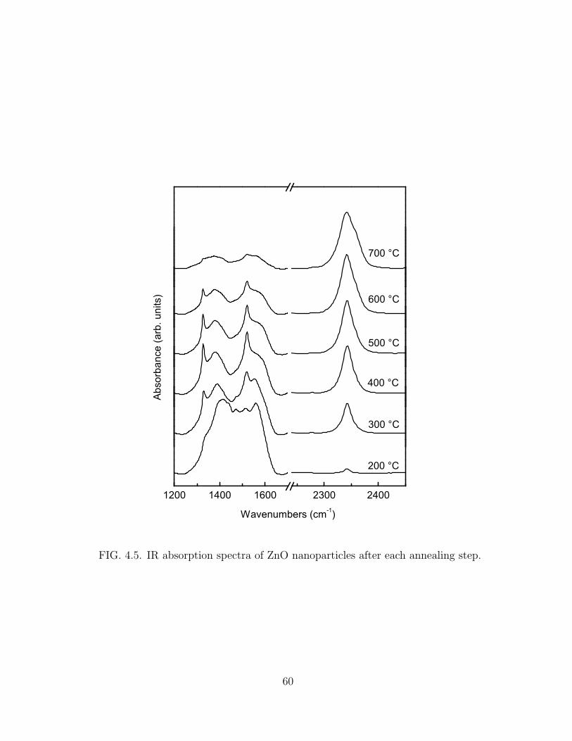
1200 1400 1600 2300 2400
200 °C
300 °C
400 °C
Wavenumbers (cm-1)
500 °C
Abs
orba
nce
(arb. u
nits
) 600 °C
700 °C
FIG. 4.5. IR absorption spectra of ZnO nanoparticles after each annealing step.
60

200 300 400 500 600 7000.0
0.2
0.4
0.6
0.8
1.0
Nor
mal
ized
Pea
k A
rea
Temperature (°C)
Carbonate Carbon Dioxide
FIG. 4.6. CO2 and carbonate peak intensities in ZnO nanoparticles after isochronalannealing. Peaks are normalized to their maxima.
61

4.4 Isotopic exchange reaction
Finally, the possibility of 12CO2 contamination from ambient air was investigated.
Fig. 4.7 shows IR spectra of samples, with the same 13C composition as sample (d),
prepared in air and argon ambients. Despite the absence of 12C atoms in the precursors,
a strong absorption peak at 2342 cm−1 appeared for the sample prepared in air.
2200 2250 2300 2350 2400
(b)
Wavenumbers (cm-1)
(a)
Abs
orba
nce
(arb. u
nits
)
FIG. 4.7. IR absorption spectra of ZnO nanoparticles, (a) prepared in air, (b) preparedin argon gas. The precursors contain only 13C isotopes [sample (d)].
This effect is presumably due to isotope exchange of 13C and 12C during the reaction
at 200 C. Post-growth annealing of sample (d) in 12CO2 gas did not result in an
increase in the 12CO2 peak, indicating that isotope exchange occurs only during the
first reaction (Eq. 4.2). During post-growth annealing, therefore, CO2 molecules are
62

produced only by thermal decomposition of the remaining carbonates in the sample
and not from the ambient.
4.5 Bonding of CO2
molecules to ZnO
To understand the nature of CO2 bonding to ZnO, we compared our results with
those of CO2 adsorption studies on ZnO surfaces [2,3]. In the adsorption process, CO2
reacts with ZnO and forms chemical species such as bidentate carbonates, polydentate
carbonates, and linear CO2. The linear molecules, which have vibrational frequencies
similar to those of free CO2, are weakly adsorbed and are not stable. They can
be immediately removed by evacuation at room temperature. This observation is
different from our results, since CO2 impurities in our samples are stable even at
elevated temperatures.
Interestingly, our results are similar to studies of trapped CO2 molecules in carbon
nanotube bundles, recently reported by Matranga et al. [4]. In their work, IR spec-
troscopy showed that thermal decomposition of oxygen-containing functionalities on
carbon nanotubes generated CO2 molecules that became permanently trapped in the
nanotube bundles. The absorption band of trapped CO2 was centered at 2330 cm−1,
which is close to that of the free molecule. They observed that those trapped molecules
persist after multiple temperature cycles and are stable for as long as 2 months in a
vacuum chamber. These results are qualitatively similar to ours. In the present work,
however, it is not known exactly where the CO2 molecules reside. It is possible, for
example, that CO2 molecules become trapped inside voids in ZnO nanoparticles.
63

4.6 Conclusions
We have observed the presence of CO2 impurities in ZnO nanoparticles by IR
spectroscopy. Isotopic substitution was used to confirm the vibrational frequency
assignment. The CO2 is formed by thermal decomposition of zinc carbonate, which
is a reaction product. The molecules are believed to be trapped within the particles,
but their exact location is not known. Further studies on the role of CO2 impurities
on the electrical and optical properties of ZnO nanoparticles will be of considerable
practical interest.
64
References
[1] Z. Wang, H. Zhang, L. Zhang, J. Yuan, S. Yan and C. Wang, Nanotechnology
14, 11 (2003).
[2] J. H. Taylor and C. H. Amberg, Can. J. Chem. 39, 535 (1961).
[3] J. Saussey, J. C. Lavalley and C. Bovet, J. Chem. Soc., Faraday Trans. I 78, 1457
(1982).
[4] C. Matranga, L. Chen, M. Smith, E. Bittner, J. K. Johnson and B. Bockrath, J.
Phys. Chem. B, 107, 12930 (2003).
65

CHAPTER 5
INFRARED AND RAMAN SPECTROSCOPY OF HYDROGEN
ANNEALED ZnO NANOPARTICLES
5.1 Introduction
Infrared reflectance spectroscopy is a useful method to determine free-carrier con-
centration in semiconductors [1,2]. In the work described in this chapter, we studied
the free-carrier concentration in ZnO nanoparticles before and after annealing in hy-
drogen, using IR reflectance and absorption spectroscopy. Electrical measurements
and Raman spectroscopy complemented the IR measurements.
5.2 Literature review
Several IR reflectance spectroscopy studies on ZnO have been performed previously.
Collins and Kleinman [3] measured reflectivity of bulk samples in the range between 1
µm and 45 µm. According to their results, for samples with free-carrier concentrations
below 1016 cm−3, the usual reflection spectrum of an ionic crystal was observed. The
Portions of this chapter were published as: W. M. Hlaing Oo, M. D. McCluskey, J. Huso, andL. Bergman, “Infrared and Raman spectroscopy ZnO nanoparticles annealed in hydrogen.” J. Appl.
Phys. 102, 043529 (2007).
66
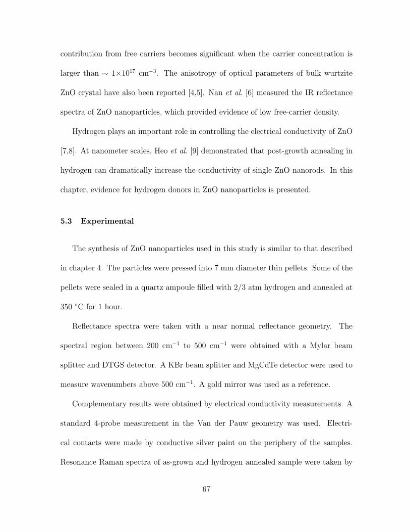
contribution from free carriers becomes significant when the carrier concentration is
larger than ∼ 1×1017 cm−3. The anisotropy of optical parameters of bulk wurtzite
ZnO crystal have also been reported [4,5]. Nan et al. [6] measured the IR reflectance
spectra of ZnO nanoparticles, which provided evidence of low free-carrier density.
Hydrogen plays an important role in controlling the electrical conductivity of ZnO
[7,8]. At nanometer scales, Heo et al. [9] demonstrated that post-growth annealing in
hydrogen can dramatically increase the conductivity of single ZnO nanorods. In this
chapter, evidence for hydrogen donors in ZnO nanoparticles is presented.
5.3 Experimental
The synthesis of ZnO nanoparticles used in this study is similar to that described
in chapter 4. The particles were pressed into 7 mm diameter thin pellets. Some of the
pellets were sealed in a quartz ampoule filled with 2/3 atm hydrogen and annealed at
350 C for 1 hour.
Reflectance spectra were taken with a near normal reflectance geometry. The
spectral region between 200 cm−1 to 500 cm−1 were obtained with a Mylar beam
splitter and DTGS detector. A KBr beam splitter and MgCdTe detector were used to
measure wavenumbers above 500 cm−1. A gold mirror was used as a reference.
Complementary results were obtained by electrical conductivity measurements. A
standard 4-probe measurement in the Van der Pauw geometry was used. Electri-
cal contacts were made by conductive silver paint on the periphery of the samples.
Resonance Raman spectra of as-grown and hydrogen annealed sample were taken by
67

cw-Kimmon laser with a wavelength 325 nm and a JY-Horiba micro-Raman/PL sys-
tem. For IR absorption spectra, hydrogen annealed nanoparticles were dispersed in
a KBr matrix (1% and 2% wt.), and IR absorption spectra were measured. A pure
KBr pellet was used as a reference to minimize the surface scattering effects. To test
the effect of ambient gas on the n-type conductivity, reflectivity measurements of a
hydrogen-annealed sample were performed with a vacuum tight chamber. The sample
was placed in the chamber and the desired gas was supplied (1 atm) after the chamber
was evacuated. After a 24 hr exposure for each gas, the sample was removed from the
chamber and reflectance spectra were recorded. The electrical conductivity measure-
ments were also done in different ambient and the results were recorded as a function
of time.
Secondary ion mass spectrometry (SIMS) was performed on an as-grown sample
and samples annealed in hydrogen and deuterium at 350 C for 1 hour. The SIMS
measurements used a 14.5 KeV Cs+ ion beam and an implanted silicon sample for deu-
terium calibration. The deuterium annealed sample showed a deuterium concentration
of 3×1020 cm−3. As shown in Fig. 5.1, the deuterium profile was constant down to the
maximum depth of the SIMS measurement (8 µm). Although SIMS cannot determine
how much hydrogen diffuses into the nanoparticles, our discussion in the next section
suggests a doping level in the 1019 cm−3 range.
68
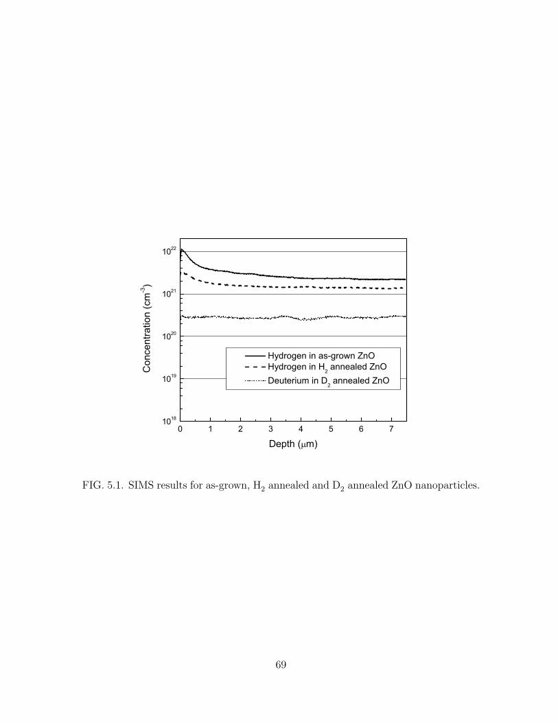
0 1 2 3 4 5 6 71018
1019
1020
1021
1022
Con
cent
ratio
n (c
m-3)
Depth ( m)
Hydrogen in as-grown ZnO Hydrogen in H
2 annealed ZnO
Deuterium in D2 annealed ZnO
FIG. 5.1. SIMS results for as-grown, H2 annealed and D2 annealed ZnO nanoparticles.
69

5.4 Results and discussion
5.4.1 IR reflectance
Reflectance spectra are shown in Fig. 5.2 for an as-grown sample and a sample
annealed in hydrogen. The reflectivity of the as-grown sample shows a sharp decrease
in reflectivity (Rmin ≈ 0) around the longitudinal optical phonon frequency ωLO. This
feature is a typical reststrahlen band reflection of semi-insulating ZnO. The hydrogen
annealed sample exhibits a change in the reststrahlen line shape, and the disappearance
of Rmin was observed. It should be noted that the nanoparticle pellets have a lower
overall reflectivity compared that of bulk ZnO, due to open voids in the sample [6].
We repeated the measurements with many different samples to ensure consistency
and reproducibility. The electrical measurements showed that the as-grown pellets are
semi-insulating (ρ ∼ 107 Ω.cm). Hydrogen annealing reduces the resistivity by several
orders of magnitude (ρ ∼ 1 Ω.cm). This result gives support to the hypothesis that
hydrogen annealing leads to an increase in free-carrier concentration. Annealing in air
or argon gas does not result in any changes in the reflectivity or conductivity.
5.4.2 Modeling
To model the reflectance spectra, we used the Lorentz-Drude model (Eq. 3.28) and
Fresnel’s equation (Eq. 3.7). The previous expressions are applicable for bulk surfaces,
but do not produce satisfactory results for nanoparticle pellets. In nanoparticles,
the existence of one free electron in a 20 nm diameter particle yields a free-carrier
70

concentration of ∼ 2 × 1017 cm−3. Since the as-grown sample is semi-insulating, we
assumed that some fraction of the particles have no free carrier (n = 0), and the
remaining particles have one electron each (∼ 2 × 1017 cm−3). For the hydrogen
annealed sample, an additional constituent of heavily doped particles (1019 cm−3)
was included. This assumption is to simplify the model; in fact, the inhomogeneity of
dopants among the nanoparticles is typically described by a binomial distribution [10].
The dielectric functions for each ZnO constituent were calculated using Eq. 3.28 with
different free-carrier concentrations, and the open voids were taken as ε = 1.
The effective dielectric function εeff for an inhomogeneous medium is given by the
Bruggeman model (Eq. 3.41), and the reflectance spectra were modeled by Eq. 3.7
with the calculated values for εeff. The surface roughness correction was applied by
Eq. 3.29. The rms value of the roughness δ was chosen as an adjustable parameter;
δ=47 nm was used in all fits.
The simulated spectra and parameters used in the fits are presented in Fig. 5.2 and
Table 5.1, respectively. Small discrepancies between the models and experiments are
due, in part, to the anisotropy of phonon frequencies and our simplified model of inho-
mogeneity. Nevertheless, the model is in good agreement with measured spectra and
it suggests that the nanoparticles have an inhomogeneous free-carrier concentration.
Due to their large surface-to-volume ratio, nanoparticles are susceptible to contam-
ination from the ambient. Fig. 5.3 shows reflectance spectra of a hydrogen-annealed
sample, measured after the sample was exposed to air. The fits to the IR spectra
indicate that the drop in reflectivity is due to a reduction in the fraction of heavily
71
200 400 600 800 10000
20
40
0
20
40
Ref
lect
ivity
(%)
Wavenumbers (cm-1)
Hydrogen-annealed
as-grown
Rmin
FIG. 5.2. Infrared reflectance spectra of ZnO nanoparticles. The dotted lines denotethe calculated spectra.
72

TABLE 5.1. Parameters used in the calculations. Constants are: ωTO = 410 cm−1,ωLO = 575 cm−1, and ε∞ = 3.75.
Sample f(%) ωp (cm−1) n(cm−3) γ (cm−1) Γ (cm−1)
As-grown30 0 0 - 5031 160 2×10¹⁷ 150 50
Hydrogen-annealed32 230 6×10¹⁷ 150 6529 1900 4×10¹⁹ 1350 60
After 1 days34 230 6×10¹⁷ 150 6527 1800 3.6×10¹⁹ 1350 60
After 21 days35 230 6×10¹⁷ 150 6026 1700 3.2×10¹⁷ 1350 60
in KBr matrix (1% wt.)0.25 230 6×10¹⁷ 150 650.275 1900 4×10¹⁹ 2550 60
in KBr matrix (2% wt.)0.5 230 6×10¹⁷ 150 650.44 1900 4×10¹⁹ 2550 60
doped particles (Table 5.1). It is possible that oxygen in ambient air could capture the
free carriers in the nanoparticles. Nanoparticles have a large surface-to-volume ratio,
and oxygen molecules can be adsorbed on the surfaces as negatively charged ions. The
adsorbed oxygen molecules transform n-type nanoparticles to a semiconducting phase.
To test this hypothesis, we investigated the stability of IR reflectivity under different
ambients. As shown in Fig. 5.4, exposure to oxygen gas results the largest drop in
the reflectivity. Small changes in the other the spectra may be due to adsorption of
oxygen from the air as the sample was transferred between the gas chamber and the
spectrometer.
Raman spectra of as-grown and hydrogenated ZnO nanoparticles are shown in
Fig. 5.5. Unlike bulk ZnO [11], LO phonon-plasmon coupling (LOPC) does not
broaden the LO phonon line shape of the doped sample. This may due to the fact
73

500 600 700 800 900 10000
5
10
15
Ref
lect
ivity
(%)
Wavenumbers (cm-1)
just after annealingafter 1 day
after 21 days
FIG. 5.3. Infrared reflectance spectra of hydrogen annealed ZnO nanoparticles afterexposure to air. The dotted lines denote the calculated spectra.
74

500 600 700 800 900 10000
5
10
15
Ref
lect
ivity
(%)
Wavenumbers (cm-1)
after annealing Vacuum Nitrogen Argon Oxygen
FIG. 5.4. IR reflectance spectra of hydrogen-annealed sample, under different ambi-ents.
75
that a significant fraction of the nanoparticles are not heavily doped. In addition, it
is conceivable that the LOPC strength is lower in nanoparticles than in bulk crystals.
Another possibility is that LOPC does not show in resonance Raman spectra (we have
not performed at non-resonance Raman measurements). A recent report [12] shows
that a broadening of the LO phonon was found in non-resonance Raman spectra of
hydrogen-annealed ZnO powder.
We also measured the IR transmittance of a hydrogen-annealed sample to de-
tect hydrogen local vibrational modes. Unfortunately, the sample was opaque to IR
radiation in the spectral range of interest (Fig. 5.6). Similar difficulties were also en-
countered in hydrogen plasma treated ZnO thin films [13]. To address that problem,
we mixed small quantities of ZnO in a KBr pellet.
5.4.3 IR absorption of hydrogen annealed ZnO nanoparticles
IR absorption spectra (Fig. 5.7) of hydrogen nanoparticles in a KBr matrix show
characteristic free-carrier absorption, as absorption increases with wavelength. To
model the absorption spectra, the modified Maxwell-Garnett (MG) model [15] was
chosen, which is appropriate for dilute quantities of ZnO in a KBr host. The effective
dielectric function is given by
εeff = εKBr
(
3 + 2∑
j fjpj
3 −∑j fjpj
)
, (5.1)
76
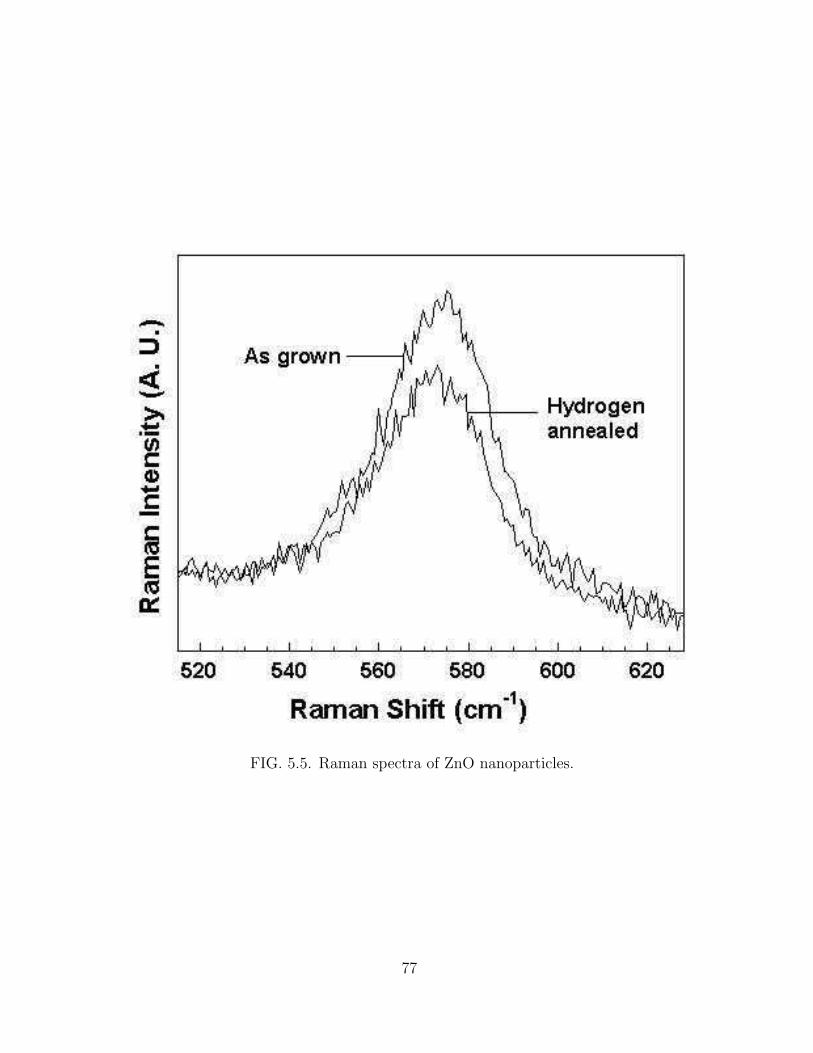
FIG. 5.5. Raman spectra of ZnO nanoparticles.
77
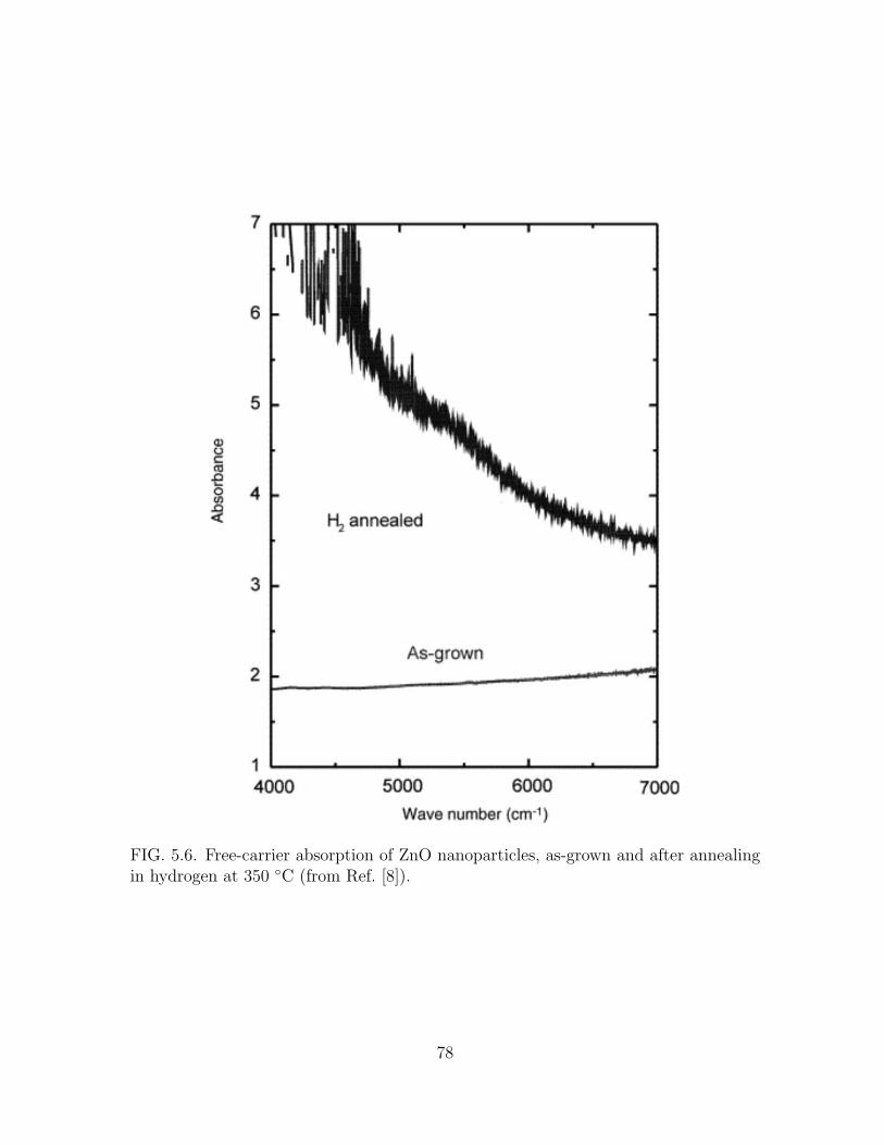
FIG. 5.6. Free-carrier absorption of ZnO nanoparticles, as-grown and after annealingin hydrogen at 350 C (from Ref. [8]).
78
where
pj = 3
(
εj − εKBr
εj + 2εKBr
)
. (5.2)
The similar procedure described previously was used to calculate the dielectric function
of ZnO nanoparticles (εj). The dielectric constant for KBr was taken as εKBr=2.34.
The absorption coefficient α was determined by Eq. 3.35. The calculated absorption
spectra show good agreement with the measured spectra (Fig. 5.7). The estimated
plasma frequencies for the reflectance and absorption spectra are also in good agree-
ment (Table 5.1).
Although hydrogen clearly affects the conductivity of ZnO nanoparticles, we were
unable to detect hydrogen related local vibrational modes (LVMs). The reason for this
null result may be that IR absorption peaks are broad such that the signal is below the
noise. Alternatively, hydrogen may modify the nanoparticle and then desorb, resulting
in an n-type defect such as an oxygen vacancy.
5.4.4 Conductivity under different ambients.
In contrast to the IR reflectivity results, the electrical conductivity of hydrogen-
annealed samples drops in all ambient conditions (Fig. 5.8). One possible reason is
that the conductivity of a pellet is dominated by grain boundaries, which is not an
issue in IR reflectivity. While the conductivity under vacuum is more stable than other
gases, it is difficult to correlate the reflectivity and conductivity results.
The effect of ambient pressure on conductivity can be seen clearly in Fig. 5.9. A
rapid change in conductivity was observed when the ambient air was allowed to interact
79
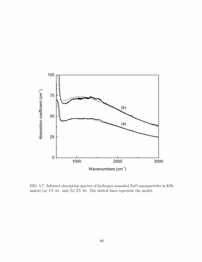
1000 2000 30000
25
50
75
100
(b)
(a)
Abs
orpt
ion
coef
ficie
nt (c
m-1)
Wavenumbers (cm-1)
FIG. 5.7. Infrared absorption spectra of hydrogen annealed ZnO nanoparticles in KBrmatrix (a) 1% wt. and (b) 2% wt. The dotted lines represent the model.
80
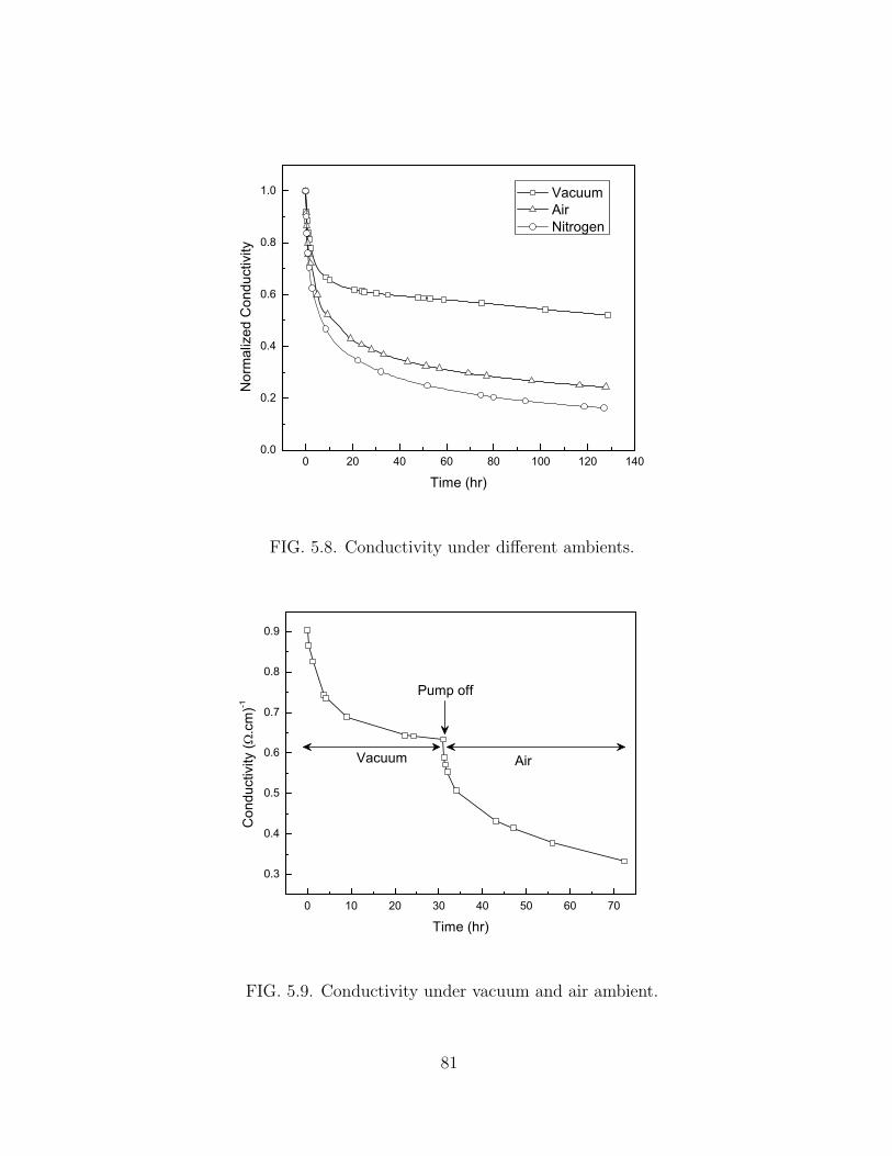
0 20 40 60 80 100 120 1400.0
0.2
0.4
0.6
0.8
1.0
Nor
mal
ized
Con
duct
ivity
Time (hr)
Vacuum Air Nitrogen
FIG. 5.8. Conductivity under different ambients.
0 10 20 30 40 50 60 70
0.3
0.4
0.5
0.6
0.7
0.8
0.9
Air
Con
duct
ivity
(.c
m)-1
Time (hr)
Pump off
Vacuum
FIG. 5.9. Conductivity under vacuum and air ambient.
81

with the sample. A similar result was also observed in nitrogen gas (Fig. 5.10).
0 2 4 6 8
0.56
0.58
0.60
0.62
N2Vacuum
N2 in
Con
duct
ivity
(.c
m)-1
Time (hr)
FIG. 5.10. Conductivity under vacuum and nitrogen ambient.
5.5 Conclusions
We demonstrated the effect of hydrogen annealing on ZnO nanoparticles. IR re-
flectance and absorption spectra indicate that hydrogen significantly increases the
free-carrier concentration. The spectra were modeled using the effective medium ap-
proximation, given an inhomogeneous free-carrier concentration. The large surface
area of nanoparticles provides adsorption sites for oxygen molecules that can cap-
ture electrons and reduce the free-electron concentration. Although the IR reflectance
spectra show significant differences between as-grown and hydrogen annealed samples,
82

Raman results do not show a statistically significant difference. These results indicate
that IR spectroscopy may provide a superior method for determining the doping level
in ZnO nanoparticles.
83

References
[1] T. S. Moss, T. D. Hawkins and G. J. Burrell, J. Phys. C: Solid State Phys. 1,
1435 (1968).
[2] W. Songprakob, R. Zallen, W. K. Liu and K. L. Bacher, Phys. Rev. B 62, 4501
(2000).
[3] R. J. Collins and D. A. Kleinman, J. Phys. Chem. Solids 11, 190 (1959).
[4] E. C. Helmetes, and H. L. Swinney, J. Appl. Phys. 38, 2387 (1967).
[5] E. F. Venger, A. V. Melnichuk, L. Y. Melnichuk and Y. A. Pasechnik, Phys. Stat.
Sol. (b) 188, 823 (1995).
[6] C. Nan, R. Birringer, W. Krauss, Haibin Gao , and H. Gleiter, Phys. Stat. Sol.
(a) 162, R3 (1997).
[7] C. G. Van de Walle, Phys. Rev. Lett. 85, 1012 (2000).
[8] M. D. McCluskey, S. J. Jokela, K. K. Zhuralev, P. J. Simpson, and K. G. Lynn,
Appl. Phys. Lett. 81, 3807 (2002).
[9] Y. W. Heo, L. C. Tien, D. P. Norton, B. S. Kang, F. Ren , B. P. Gila and S. J.
Pearton, Appl. Phys. Lett. 85, 2002 (2004).
[10] J. D. Bryan and D. R. Gamelin, Progress in Inorganic Chemistry 54, 74 (2005).
[11] B. H. Bairamov, A. Heinrich, G. Iremer, V. V. Toporov, and E. Ziegler, Phys.
Stat. Sol. (b) 119, 227 (1983).
[12] C. F. Windisch, G. J. Exarhos, C. Yao, and L. Wang, J. Appl. Phys. 101, 123711
(2007).
84

[13] C. A. Wolden, T. M. Barnes, J. B. Baxter and E. S. Aydil, J. Appl. Phys. 97,
043522 (2005).
[14] M. D. McCluskey, S. J. Jokela and W. M. Hlaing Oo, Physica B 376-377, 690
(2006).
[15] C. G. Granqvist and O. Hundrei, Phys. Rev. B 16, 3513 (1977).
85

CHAPTER 6
INFRARED SPECTROSCOPY OF COPPER DOPED ZnO
NANOPARTICLES.
Copper impurities play an important roles in the optical and electrical properties
of ZnO. In this work, I present the IR optical transition spectra of Cu ions in ZnO
nanoparticles.
6.1 Copper impurities in ZnO
Copper, a 3d transition metal, is incorporated into the ZnO lattice by substituting
Zn sites. The substitution leads the Cu impurity to assume the charge state of Cu2+
(3d94s2). The Cu2+ ion can also capture an extra electron and transform to the Cu+
(3d104s2) state. The electronic states of Cu2+ ions can be described by crystal field
splitting. When an impurity atom is placed within the crystal field of surrounding
atoms, the energy levels of the atom are perturbed by the crystal field, resulting in the
splitting of degenerate states. In a cubic tetrahedral field, the d electron orbital splits
into an upper 2T and lower 2E states (Fig. 6.1). Both 2T and 2E states are located
just below the conduction band; thus, the Cu2+ impurity acts as a deep acceptor.
86
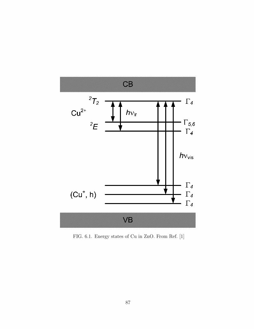
FIG. 6.1. Energy states of Cu in ZnO. From Ref. [1]
87

6.2 Experimental
A similar procedure to that described in Chapter 4 was used to synthesize Cu
doped ZnO nanoparticles. Instead of using pure zinc acetate, a Cu doped zinc acetate
precursor was used. For the precursor preparation, 9.0 g of Zn(CH3COO2) · 2H2O was
dissolved in 20 ml of water at 80 C, and 0.07 g of Cu(CH2COO)2 was added. The
solution was cooled down to room temperature and kept for 1 day to allow the crystal
to grow. Then, the crystals were collected and dried at room temperature. Using
this precursor, nanoparticles were grown. The as-grown ZnO:Cu nanoparticles show
a faint greenish color.
The ZnO:Cu powder was pressed into a thin pellet to measure the IR spectrum.
The sample was mounted inside a liquid helium cooled cryostat and the IR spectrum
was taken at 9 K. A Ge:Cu detector was used. The spectrum was averaged over 500
scans and the spectral resolution was 1 cm−1.
6.3 Results
The IR absorption spectrum is presented in Fig. 6.2. Two absorption peaks were
observed at energies of 5781 cm−1 and 5821 cm−1. These absorption peaks arise from
internal transitions of Cu2+ ions between the 2T state and two sublevels of the 2E
state. Similar absorption lines were also observed in bulk ZnO [2,3]. The width of the
absorption peaks in our nanoparticles are broader than that of bulk crystals.
In some samples, a series of unidentified peaks were also observed in the region
88

of 3500-3800 cm−1 (Fig. 6.3). Those peaks were found only in Cu-doped samples.
Samples that showed a high degree of residual water contamination, however, did
not show these peaks. We note that absorption peaks related to CuO and Cu2O
phases were not observed, indicating that the nanoparticles were free from copper
oxide phases.
We measured the electrical resistivity of ZnO:Cu nanoparticle pellets and unfor-
tunately reliable results were not obtainable. The typical resistivity of undoped ZnO
nanoparticle pellet is ∼ 107 Ω.cm (see Ch. 5), and Cu doped particles are likely to
have even lower free carrier concentrations than undoped particles. That property is
similar to bulk samples in which n-type dopants are compensated by Cu acceptors.
6.4 Conclusions
We showed that ZnO nanoparticles can be doped with Cu by using a Cu-doped
zinc acetate precursor. The electronic transitions of Cu2+ ions were observed in the
IR absorption spectrum at low temperatures, which is an evidence of Cu substitution
for Zn atoms. The high resistivity property indicates that the copper deep acceptor
could capture a free electron from conduction band. We plan to investigate this topic
further, starting in January 2008.
89

5700 5750 5800 5850 5900 5950
Abs
orba
nce
(arb. u
nits
)
Wavenumbers (cm-1)
5781 cm-1
5821 cm-1
FIG. 6.2. IR absorption spectrum of ZnO:Cu nanoparticles at 9 K.
3500 3550 3600 3650 3700 3750 3800
Abs
orba
nce
(arb. u
nits
)
Wavenumbers (cm-1)
FIG. 6.3. IR absorption spectrum of ZnO:Cu nanoparticles at 9 K (3500-3800 cm−1
region)
90

References
[1] P. Dahan, V. Fleurovy, P. Thurianz, R. Heitzz, A. Hoffmannz, and I. Broserz, J.
Phys. Condens. Matter 10, 2007 (1998).
[2] R. E. Dietz, H. Kamimura, M. D. Struge, and A. Yariv, Phys. Rev. 132, 1559
(1963).
[3] N. Y. Garces, L. Wang, L. Bai, N. C. Giles, L. E. Halliburton, and G. Cantwell,
Appl. Phys. Lett. 81, 622 (2002).
91
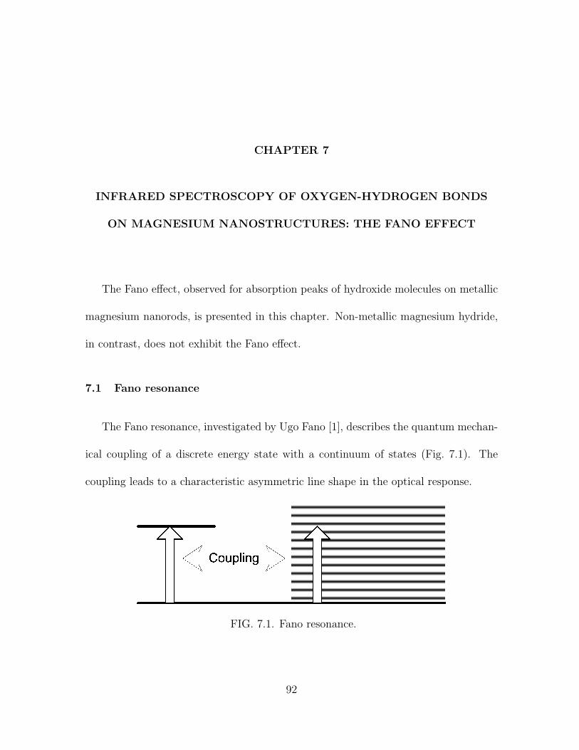
CHAPTER 7
INFRARED SPECTROSCOPY OF OXYGEN-HYDROGEN BONDS
ON MAGNESIUM NANOSTRUCTURES: THE FANO EFFECT
The Fano effect, observed for absorption peaks of hydroxide molecules on metallic
magnesium nanorods, is presented in this chapter. Non-metallic magnesium hydride,
in contrast, does not exhibit the Fano effect.
7.1 Fano resonance
The Fano resonance, investigated by Ugo Fano [1], describes the quantum mechan-
ical coupling of a discrete energy state with a continuum of states (Fig. 7.1). The
coupling leads to a characteristic asymmetric line shape in the optical response.
FIG. 7.1. Fano resonance.
92
The superposition of a discrete state |ϕ〉 and continuum state |ψE′〉 can be written
as
ΨE = aϕ|ϕ〉 +
∫
bE′|ψE′〉dE ′. (7.1)
The transition probabilities from the initial state |i〉 to the perturbed |ΨE〉 and
unperturbed |ψE > continuum states are 〈ΨE|T |i〉 and 〈ψE|T |i〉 respectively. The
Fano line shape is given by the ratio of the two transition probabilities,
〈ΨE|T |i〉〈ψE|T |i〉
=(q + ε)2
1 + ε2. (7.2)
The variable ε is defined as a reduced energy:
ε =2(E − E0)
Γ, (7.3)
where E0 is the resonance energy with a width Γ.
Detailed derivations of the Fano function can be found in Refs. [1,2]. The param-
eter q is the asymmetry parameter, which determines the asymmetric feature of the
peak line shape and hence the degree of coupling. The Fano line shape approaches a
symmetric Lorentzian shape as q → ∞. Plots of the Fano line shape with different q
values are presented in Fig. 7.2.
Although the theory was initially developed for autoionization of atoms, the Fano
effect has been observed in a wide range of areas such as IR absorption lines of ad-
sorbates on thin metal films [3], Raman line shapes [4,5], and local vibrational modes
93

-8 -6 -4 -2 0 2 4 6 8
q=0
q=0.5
q=1
q=2
(q
+)2 /(
1+)2
q=3
FIG. 7.2. Fano line shape with different q values.
94

(LVMs) in heavily doped semiconductors [6,7].
7.2 Fabrication of magnesium nanorods
The Mg nanorods 1 were fabricated by the glancing angle deposition (GLAD) tech-
nique [8]. The sample fabrication was performed in a high vacuum chamber with a
background pressure of 3 × 10⁻⁷ Torr. The Mg (99.95 %, from CERAC, Inc.) source
was evaporated by electron beam bombardment. The pressure during deposition was
less than 1 × 10⁻⁶ Torr, and the growth rate was monitored by a quartz crystal mi-
crobalance (QCM) and was fixed at 0.5 nm/s. The incident angle of vapor flux with
respect to the substrate normal was fixed at 86. The distance between the evapo-
ration source and the substrate was approximately 20 inches. Using these deposition
parameters, a layer of Mg nanorods with a nominal thickness (QCM reading) of 4 mm
was grown on Si (100) substrate. A scanning electron microscope (SEM) image of Mg
nanorods is shown in Fig. 7.3.
7.3 Experimental
The magnesium nanorods sample was reacted with a boiling H2O-D2O mixture
for 5 min, and dried in the air at 150 C for 5 min. IR spectra were taken at room
temperature. The spectral resolution was 4 cm−1 and the spectra were averaged over
500 scans. A KBr beam splitter and liquid nitrogen cooled MgCdTe detector were
used. The spectrum from a plain silicon substrate was used as a reference to calculate
1Mg nanorods and SEM image were provided by Prof. Yiping Zhao’s group (University of Geor-gia).
95

FIG. 7.3. SEM image of Mg nanorods on a Si substrate.
the absorbance spectra.
A similar procedure was performed to produce Mg(OH)2 from commercial Mg and
MgH2 powder. The materials were obtained from Sigma-Aldrich and experiments
were done without further purification. The powder samples were diluted with KBr
powder and pressed into thin pellets to measure IR absorption. The IR spectrum of a
pure KBr pellet was used as a reference. An X-ray diffraction (XRD) spectrum of Mg
powder after reaction with water was taken to determine whether bulk Mg(OH)2 was
formed.
7.4 Results and discussions
Absorption peaks at 3699 cm−1 and 2712 cm−1 were observed (Fig. 7.4) and as-
signed as vibrational frequency of OH and OD from the magnesium hydroxide com-
pounds [9]. The asymmetric line shape feature was observed in both OH and OD ab-
sorption peaks. The appearance of a Fano line shape in Mg samples is due to coupling
96
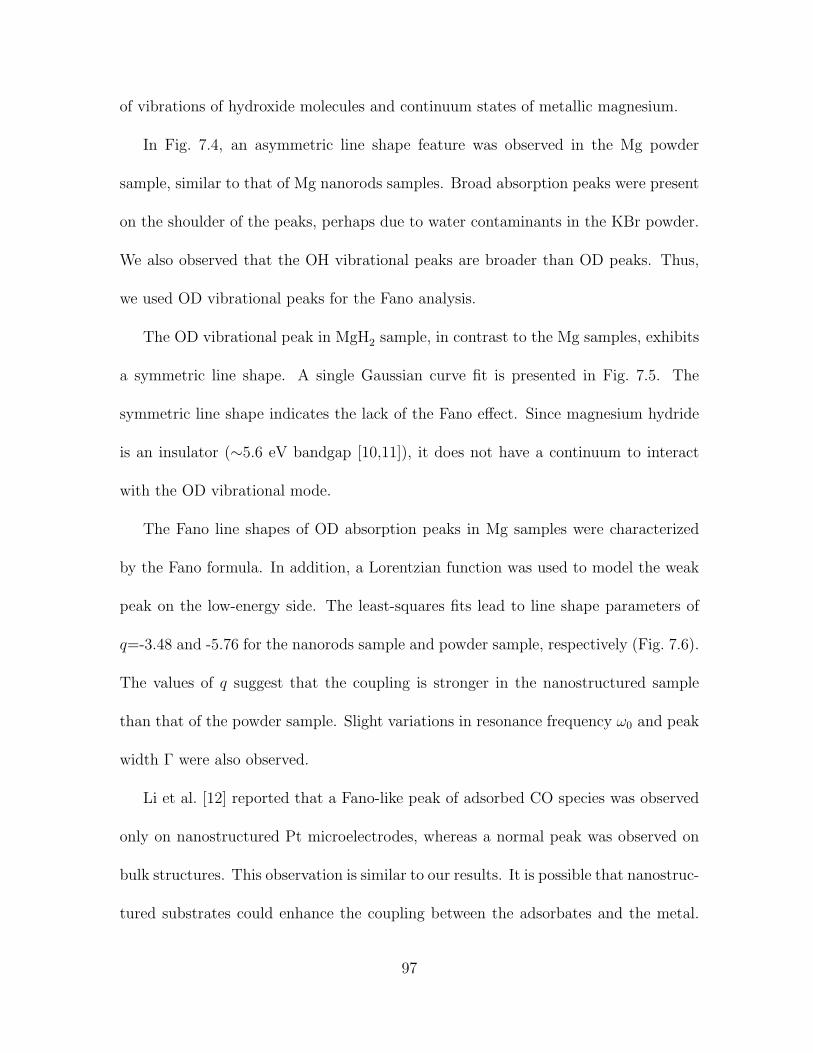
of vibrations of hydroxide molecules and continuum states of metallic magnesium.
In Fig. 7.4, an asymmetric line shape feature was observed in the Mg powder
sample, similar to that of Mg nanorods samples. Broad absorption peaks were present
on the shoulder of the peaks, perhaps due to water contaminants in the KBr powder.
We also observed that the OH vibrational peaks are broader than OD peaks. Thus,
we used OD vibrational peaks for the Fano analysis.
The OD vibrational peak in MgH2 sample, in contrast to the Mg samples, exhibits
a symmetric line shape. A single Gaussian curve fit is presented in Fig. 7.5. The
symmetric line shape indicates the lack of the Fano effect. Since magnesium hydride
is an insulator (∼5.6 eV bandgap [10,11]), it does not have a continuum to interact
with the OD vibrational mode.
The Fano line shapes of OD absorption peaks in Mg samples were characterized
by the Fano formula. In addition, a Lorentzian function was used to model the weak
peak on the low-energy side. The least-squares fits lead to line shape parameters of
q=-3.48 and -5.76 for the nanorods sample and powder sample, respectively (Fig. 7.6).
The values of q suggest that the coupling is stronger in the nanostructured sample
than that of the powder sample. Slight variations in resonance frequency ω0 and peak
width Γ were also observed.
Li et al. [12] reported that a Fano-like peak of adsorbed CO species was observed
only on nanostructured Pt microelectrodes, whereas a normal peak was observed on
bulk structures. This observation is similar to our results. It is possible that nanostruc-
tured substrates could enhance the coupling between the adsorbates and the metal.
97

2600 2700 3600 3700 3800
(c)
(b)
Wavenumbers (cm-1)
(a)
Abs
orba
nce
(arb. u
nits
)
FIG. 7.4. OH and OD absorption peaks on (a) Mg nanorods, (b) Mg powder, and (c)MgH2 powder.
98

2650 2700 2750 2800
Abs
orba
nce
(arb. u
nits
)
Wavenumbers (cm-1)
FIG. 7.5. Gaussian line shape fit of OD absorption peak in the MgH2 sample.
99
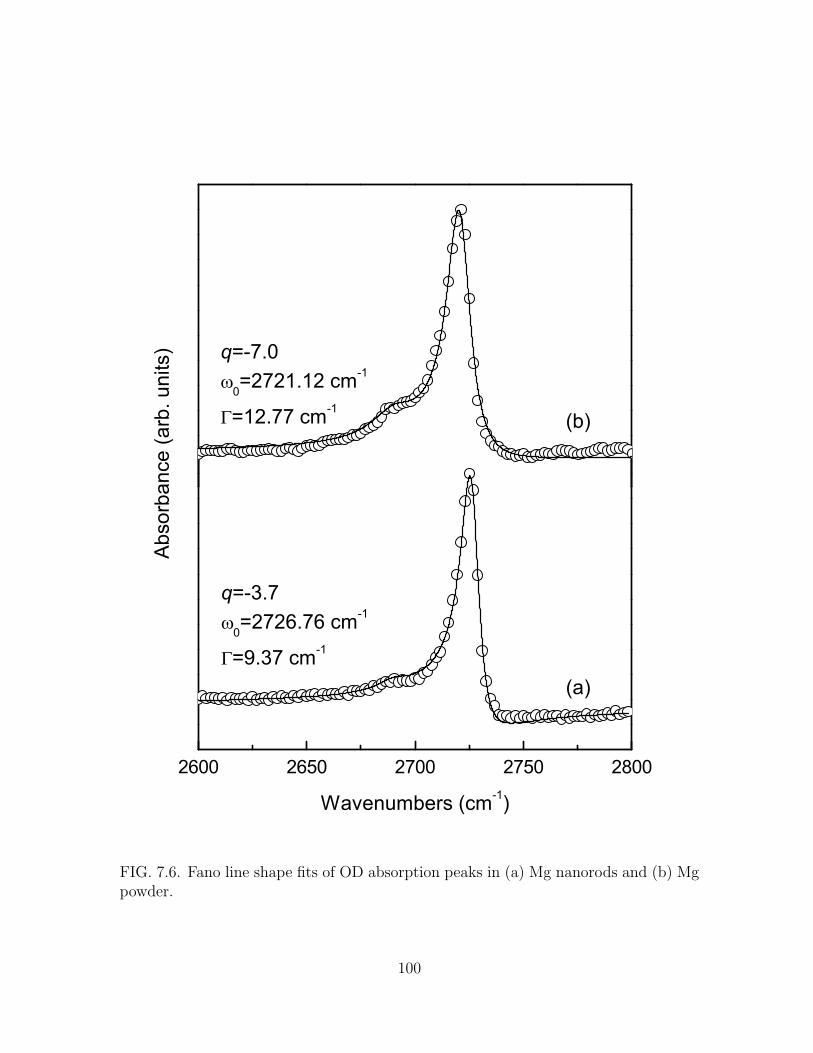
2600 2650 2700 2750 2800
q=-3.7
0=2726.76 cm-1
=9.37 cm-1
(b)
Abs
orba
nce
(arb. u
nits
)
Wavenumbers (cm-1)
(a)
q=-7.0
0=2721.12 cm-1
=12.77 cm-1
FIG. 7.6. Fano line shape fits of OD absorption peaks in (a) Mg nanorods and (b) Mgpowder.
100
The frequency shift and shape of the vibrational spectra also depend on the thickness
and surface morphology of the metal films [13]. The different morphology between
nanorods and powder samples may cause slight variations in the resonance frequency
and width of the absorption peaks.
The XRD pattern of Mg powder after reaction of water is shown in Fig. 7.7. From
the spectrum, it can be seen that all diffraction peaks indicate only the magnesium
structure. The lack of a Mg(OH)2 structure provides evidence that the hydroxide
forms only a thin layer over the magnesium surfaces, and their quantity is under
the detection limit of XRD. Hence, similar to adsorbate molecules, the vibrations of
molecules from such a thin layer couple with continuum states.
10 20 30 40 50 60 70
Mg(10
0)
Mg(20
0)
Mg(10
3)
Mg(11
0)
Mg(10
2)
Mg(10
1)
Inte
nsity
(arb. u
nits
)
2 Theta
Mg(00
2)
FIG. 7.7. XRD pattern of Mg powder after reaction with water.
101

7.5 Conclusions
In conclusion, the coupling between vibrations of hydroxide molecules and con-
tinuum electronic states from metallic magnesium results in an asymmetric Fano line
shape in absorption peaks, as observed with IR absorption spectroscopy. For the insu-
lator MgH2, the symmetric Gaussian absorption line shape was observed. The XRD
pattern suggests that a thin hydroxide layer forms on the metallic surfaces. The OH
(or OD) molecules are in close proximity to the metallic continuum and hence show
significant coupling.
102

References
[1] U. Fano, Phys. Rev. 124, 1866 (1961).
[2] J.-P. Connerad, Highly Excited Atoms(Cambridge Uniersity Press, 1998).
[3] O. Krauth, G. Fahsold, N. Magg, and A. Pucci, J. Chem. Phys. 113, 6330 (2000).
[4] J. W. Ager III, W. Walukiewicz, M. McCluskey, M. A. Plano, and M. I. Land-
strass, Appl. Phys. Lett. 66, 616 (1995).
[5] N. H. Nickel, P. Lengsfeld, and I. Sieber, Phys. Rev. B 61, 15558 (2000)
[6] R. E. Prichard, B. R. Davidson, R. C. Newman, T. J. Bullought, T. B. Joyce, R.
Jones, and S. Oberg, Semicond. Sci. Technol. 9, 140 (1994).
[7] M. Stavola, S. J. Pearton, J. Lopata, and W. C. Dautremont-Smith, Phys. Rev.
B 37, 8313 (1988).
[8] Y. P. He, J. X. Fu, Y. Zhang, Y. P. Zhao, L. J. Zhang, A. L. Xia, J. W. Cai,
Small, 3, 153 (2007).
[9] E.F. de Oliveira, Y. Hase, Vibrational Spectroscopy 25, 53 (2001).
[10] J. Isidorsson, I. A. M. E. Giebels, H. Arwin, and R. Griessen. Phys. Rev. B 68,
115112 (2003).
[11] M. J. van Setten, V. A. Popa, G. A. de Wijs, and G. Brocks, Phys. Rev. B 75,
035204 (2007).
[12] J. Li, Q. Chen, and S. Sun, Electrochimica Acta 52, 5725 (2007).
[13] O. Krauth, G. Fahsold, A. Pucci-Lehmann, J. Molecular Structure, 482-483, 237
(1999).
103

APPENDIX A
Vibrations of linear tri-atomic molecules
FIG. A.1. Linear tri-atomic molecule.
Consider a linear tri-atomic molecule as shown in the Fig. A.1. We can write the
equations of motion as:
md2x1
dt2+ κ(x2 − x1) = 0,
Md2x2
dt2+ κ(2x2 − x1 − x3) = 0,
md2x3
dt2+ κ(x3 − x2) = 0.
(A.1)
Using the trial solution
xi = x0i exp(iωt), (A.2)
d2xi
dt2= −ω2xi. (A.3)
104

By substituting Eq. A-3 into Eq. A-1, we obtained
(κ−mω2)x1 − κx2 = 0,
−κx1 + (2κ−Mω2)x2 − κx3 = 0,
−κx2 + (κ−mω2)x3 = 0.
(A.4)
The homogeneous linear equations can be solved by a determinant:
κ−mω2 −κ 0
−κ 2κ−Mω2 −κ
0 −κ κ−mω2
= 0. (A.5)
Ths solution leads to
ω2(κ−mω2)(Mmω2 − κM − 2κm) = 0. (A.6)
Thus,
ω1 = 0, (A.7)
ω2 =
√
κ
m, (A.8)
ω3 =
√
κ
(
2
M+
1
m
)
. (A.9)
105
APPENDIX B
MOCVD growth ZnO thin films.
This work is an initial part of an ongoing project (EMSL proposal No. 22290) at
Pacific Northwest National Laboratory. Since the work is still in an initial stage, the
recent results are included in this dissertation as an appendix.
A wide variety of thin film growth techniques have been utilized to grow oriented
or epitaxial ZnO thin films [1]. Metal organic chemical vapor deposition (MOCVD)
has been one of the popular techniques to grow ZnO due to its high throwing power,
scalability in operation and high purity of the precursor solutions. The MOCVD sys-
tem (Fig, B.1) uses metal organic compounds as precursors. The carrier gas is injected
into the liquid to transfer the precursors into higher temperature zone evaporator and
growth chamber. The precursors are then thermally decomposed and formed atomic
layer on the substrate. The challenges for CVD precursor volatility can be tackled by
using appropriately designed main and dopant precursors which decompose at simi-
lar temperatures. Precursor such as Bis(2,2,6,6-tetramethyl-3,5-heptanedionato)Zinc
[Zn(TMHD)2] provides a good compromise between appropriate volatility and envi-
ronmental friendliness with less carbon contamination in the films [2].
106

FIG. B.1. Schematic diagram of MOCVD system.
B1. Experimental
A cold-wall Emcore MOCVD system at Environmental Molecular Sciences Labo-
ratory, PNNL was used to grow the ZnO thin-films. The zinc [Zn(TMHD)2] and man-
ganese [Mn(TMHD)2] precursors were dissolved in tetrahydrofuran (THF) solution to
a molar concentration of 0.025 M. The depositions were made on c-plane sapphire and
silicon (100) oriented substrates. The Mn concentrations were varied by adjusting Zn
and Mn precursors flow rate during the deposition. Visually a more yellowish color
appearance was observed in the films with higher Mn contents. The nitrogen was used
as carrier gas. For better oxidation, oxygen gas was also injected into reactor. We
note that the thickness of ZnO films has a linear relationship with partial deposition
pressure in the range of 5-60 Torr. This situation is typically present when a feed
rate limited condition during the deposition exists. We also note that changing the
precursor flow rates in the range of 50-100 g/hr does not significantly alter the film
107
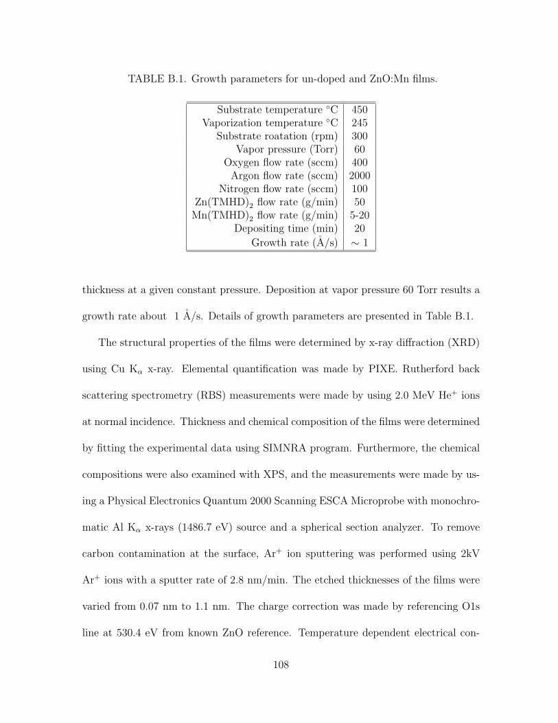
TABLE B.1. Growth parameters for un-doped and ZnO:Mn films.
Substrate temperature C 450Vaporization temperature C 245
Substrate roatation (rpm) 300Vapor pressure (Torr) 60
Oxygen flow rate (sccm) 400Argon flow rate (sccm) 2000
Nitrogen flow rate (sccm) 100Zn(TMHD)2 flow rate (g/min) 50Mn(TMHD)2 flow rate (g/min) 5-20
Depositing time (min) 20
Growth rate (A/s) ∼ 1
thickness at a given constant pressure. Deposition at vapor pressure 60 Torr results a
growth rate about 1 A/s. Details of growth parameters are presented in Table B.1.
The structural properties of the films were determined by x-ray diffraction (XRD)
using Cu Kα x-ray. Elemental quantification was made by PIXE. Rutherford back
scattering spectrometry (RBS) measurements were made by using 2.0 MeV He+ ions
at normal incidence. Thickness and chemical composition of the films were determined
by fitting the experimental data using SIMNRA program. Furthermore, the chemical
compositions were also examined with XPS, and the measurements were made by us-
ing a Physical Electronics Quantum 2000 Scanning ESCA Microprobe with monochro-
matic Al Kα x-rays (1486.7 eV) source and a spherical section analyzer. To remove
carbon contamination at the surface, Ar+ ion sputtering was performed using 2kV
Ar+ ions with a sputter rate of 2.8 nm/min. The etched thicknesses of the films were
varied from 0.07 nm to 1.1 nm. The charge correction was made by referencing O1s
line at 530.4 eV from known ZnO reference. Temperature dependent electrical con-
108

ductivity measurements were made in standard 4-probe van der Pauw geometry. The
films grown on single crystal sapphire substrates were used for electrical conductivity
measurements.
B2. Results and discussion
The XRD spectra of undoped and Mn doped films grown on Si(100) single crystals
show dominant peaks for ZnO (002) plane and (004) plane (Fig. B.2). The results
confirm that the films are well-oriented along the c-axis. Within XRD detection limit,
no secondary phase formation related to Mn-O is detected. The as-recorded c-axis
lattice parameter for undoped sample was 5.20 A. After assuming that the films are
completely relaxed due to its 100 nm thickness and expected defects in it, the c-axis
lattice parameters for Mn doping of ∼1.5 atom % and 4.5 atom % ZnO films are
observed to be slightly increased to 5.21 and 5.22 , respectively. This shift to lower
angle as a function of Mn incorporation is shown as an inset of Figure 1. Hence, the
possible substitution of Mn2+ for Zn2+ expands the lattice parameter due to the larger
ionic radius of Mn2+ ion. In addition, the lack of major structural disorder in doped
films was confirmed by the consistency of peak widths without further broadening. A
similar increase in the ZnO lattice parameter with addition of Mn was also noticed by
Chikoidze et al. [3,4]
PIXE is highly sensitive to elemental analysis and thus is an excellent technique
to quantify the overall concentration of host as well as dopant materials. A typical
PIXE spectrum for the 3% atom %. Mn doped films grown on Si (100) a single
109
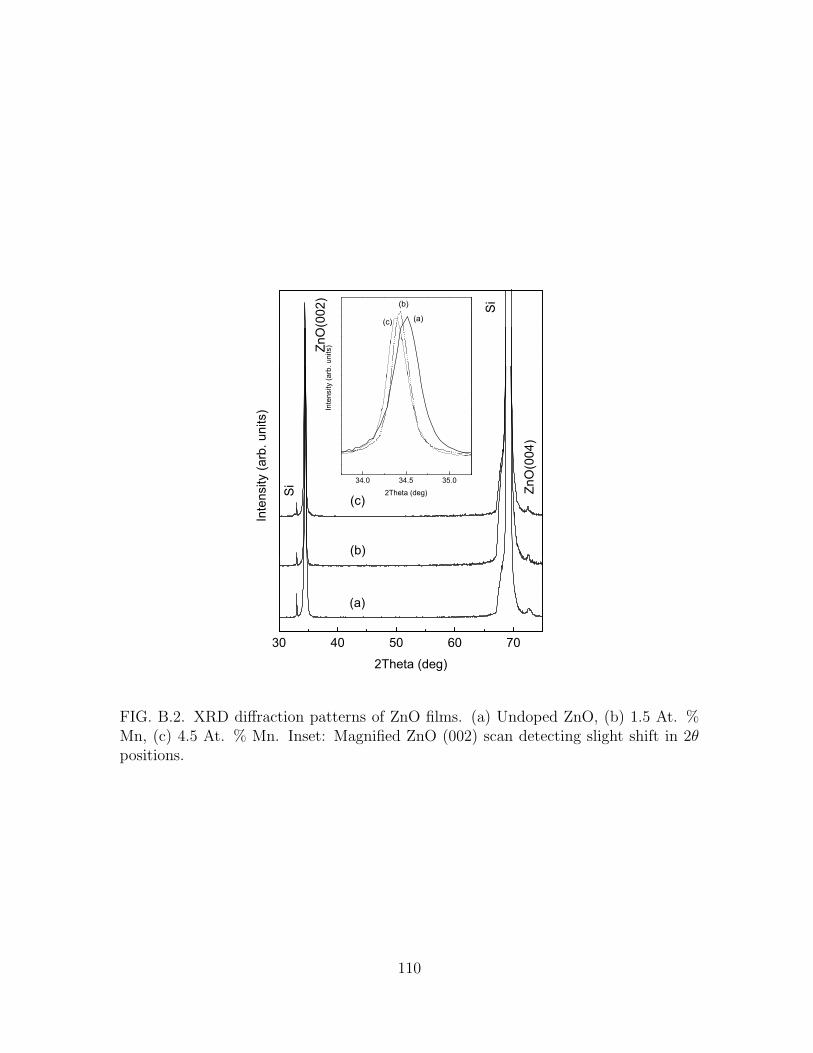
30 40 50 60 70
2Theta (deg)
(c)
(b)
(a)
Si
Si
34.0 34.5 35.0
(c)
(b)
Inte
nsity
(arb. u
nits
)
2Theta (deg)
(a)
ZnO
(004
)
In
tens
ity (a
rb. u
nits
)
ZnO
(002
)
FIG. B.2. XRD diffraction patterns of ZnO films. (a) Undoped ZnO, (b) 1.5 At. %Mn, (c) 4.5 At. % Mn. Inset: Magnified ZnO (002) scan detecting slight shift in 2θpositions.
110

crystal is shown in Fig. B.3. The Mn Kα emission along with Zn and Si peaks, can be
clearly seen in the spectrum. The inset of Fig. B.3 represents RBS spectra of the same
Mn:ZnO film grown on a Si (100) single crystal. The overall uniformity in the Mn
distribution can be realized in the spectrum. We also use these data for the calculation
of film thickness 100 nm. From the curve profile, no noticeable diffusion of the film
into the substrate is observed. High resolution XPS spectra for the regions of Zn 2p,
O 1s, Mn 2p and Mn 3p are shown in Figs. B.4 and B.5. The intensity ratios between
O to Zn were mostly un-affected by Mn incorporation. Despite the lack of Mn dopant
in undoped ZnO sample, there is a weak and broad peak exhibits at an energy around
640 eV, which is Auger (AES) line of Zn 2p state (Fig. B.5) originating from Auger
emission of Zn atoms. Hence, instead of using Mn 2p peak, we used weaker Mn 3p
peak for the analysis of Mn composition, so that we can avoid the convolution of Zn
Auger emission. The Mn 2p and Mn 3p peak positions and widths are consistent for
all Mn contents which indicate that Mn2+ state is dominant in all doped films.
The ratio of zinc to oxygen compositions as a function of Mn content calculated
from both XPS and PIXE are presented in Fig. B.6. The data are presented in four
different sets as (a) from PIXE technique, (b) As recorded XPS surface scan, (c) After
Ar+ ion sputtering in XPS and (d) XPS corrected atomic concentration, respectively.
One of the major reasons for presenting the data in such a way is to discuss the role of
surface carbon, and hydrocarbons in XPS technique, adjusting it with correction and
comparing with independent PIXE technique. As shown in Fig, 5(b), by calculating
the ratio of Zn to O peaks in as-recorded sample, we have seen significant variation in
111

0 2 4 6 8 10
200 300 400 500 600 700 800
Ba
cksc
atte
ring
Yiel
d (a
rb. u
nits
)
Channel Number
O
Si
ZnSi k
Zn kZn k
X-r
ay y
ield
(arb. u
nits
)
X-ray Energy (keV)
Mn k
FIG. B.3. PIXE spectrum of ZnO:Mn (4.5 At. % Mn) sample. RBS spectrum isshown in inset. The solid lines represent the modeled spectra.
112

520 530 1020 1040 1060
Zn 2p
ZnO ZnO:Mn (Mn 1.5 At. %) ZnO:Mn (Mn 4.5 At. %)
Inte
nsity
(arb. u
nits
)
Binding Energy (eV)
O 1s
FIG. B.4. XPS spectra for ZnO and ZnO:Mn films. Zn and O regions.
30 40 50 630 640 650
Mn 2p
Mn 3p ZnO ZnO:Mn (Mn 1.5 At. %) ZnO:Mn (Mn 4.7 At. %)
Inte
nsity
(arb. u
nits
)
Binding Energy (eV)
FIG. B.5. XPS spectra for ZnO and ZnO:Mn films. Mn regions.
113
it with Mn addition. By considering the peaks for surface hydrocarbons and correcting
it in the total, we have seen that variation in the Zn to O peak ratio was somewhat
reduced. Ar+ ion sputtering was used to remove surface layers and XPS analysis
after sputtering indicates substantial removal of the surface hydrocarbons. As seen in
Fig. 5(d), the variation in Zn to O peak ratio as a function of Mn addition narrowed
considerably as a result of cleaning of surface contaminants and hydrocarbons. For
most part, the XPS ratio analysis indicates Zn rich films. Some of the major reasons for
it can be oxygen sensitivity factor is different than Zn sensitivity factor. Also as noted
previously oxygen is known to sputter out preferentially [5]. However, even though
not detected in our analysis, we can not completely rule out minor percentage of sub-
stoichometric ZnO. As seen in Fig. B.6a, after comparing the data with completely
independent and sensitive PIXE technique, we have seen that the ratio of Zn to O
gradually decreases from near 1 as a function of Mn doping concentration in ZnO
films, which should be an expected outcome. We would like to also note that the slight
differences in Mn atomic concentrations calculated by PIXE and XPS techniques are
due to differences in the sensitivity factors, usage of 3p line instead of 2p line, and
normalization process during calculations in the case of XPS analysis.
The temperature dependent conductivity results indicate that conductivity de-
creases with increasing Mn content in ZnO (Fig. B.7). The results are in good agree-
ment with other reports of Mn doped ZnO [6,7]. By using the relationship between
conductivity of semiconductor as a function of temperature [σ ∝ exp(−∆E/kT )], the
trends for all films are more or less similar. The estimated activation energy for all
114
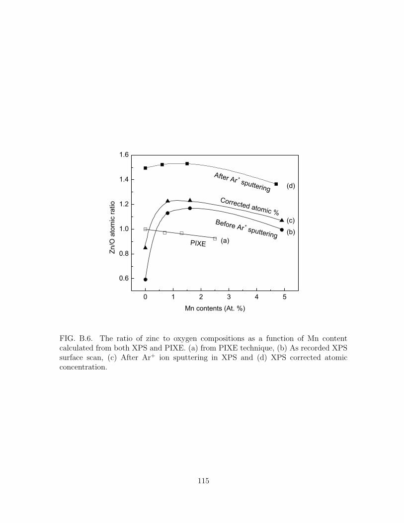
0 1 2 3 4 5
0.6
0.8
1.0
1.2
1.4
1.6
PIXE
Before Ar + sputtering
Corrected atomic %
(d)
(c)
(b)
Zn/O
ato
mic
ratio
Mn contents (At. %)
(a)
After Ar + sputtering
FIG. B.6. The ratio of zinc to oxygen compositions as a function of Mn contentcalculated from both XPS and PIXE. (a) from PIXE technique, (b) As recorded XPSsurface scan, (c) After Ar+ ion sputtering in XPS and (d) XPS corrected atomicconcentration.
115
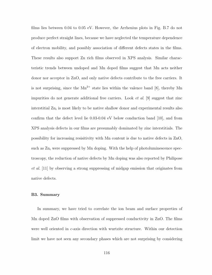
films lies between 0.04 to 0.05 eV. However, the Arrhenius plots in Fig. B.7 do not
produce perfect straight lines, because we have neglected the temperature dependence
of electron mobility, and possibly association of different defects states in the films.
These results also support Zn rich films observed in XPS analysis. Similar charac-
teristic trends between undoped and Mn doped films suggest that Mn acts neither
donor nor acceptor in ZnO, and only native defects contribute to the free carriers. It
is not surprising, since the Mn2+ state lies within the valence band [8], thereby Mn
impurities do not generate additional free carriers. Look et al. [9] suggest that zinc
interstitial Zni is most likely to be native shallow donor and experimental results also
confirm that the defect level lie 0.03-0.04 eV below conduction band [10], and from
XPS analysis defects in our films are presumably dominated by zinc interstitials. The
possibility for increasing resisitivity with Mn content is due to native defects in ZnO,
such as Zni were suppressed by Mn doping. With the help of photoluminescence spec-
troscopy, the reduction of native defects by Mn doping was also reported by Philipose
et al. [11] by observing a strong suppressing of midgap emission that originates from
native defects.
B3. Summary
In summary, we have tried to correlate the ion beam and surface properties of
Mn doped ZnO films with observation of suppressed conductivity in ZnO. The films
were well oriented in c-axis direction with wurtzite structure. Within our detection
limit we have not seen any secondary phases which are not surprising by considering
116
3 4 5 6 7 8 9 10 1110-5
10-4
10-3
10-2
ZnO ZnO:Mn (Mn 1.5 At. %) ZnO:Mn (Mn 4.7 At. %)
Con
duct
ivity
(.c
m)-1
1000/T(K)
FIG. B.7. Temperature dependent electrical conductivity for undoped as well asZnO:Mn films.
117

relatively low Mn doping concentration. The RBS measurements also confirm uniform
distribution of Mn dopants throughout the film. Electrical conductivity results prove
the conductivity suppressing nature of Mn2+ ions in ZnO host. The XPS results show
that Mn2+ state is most likely to be dominant state. Thus, impact of Mn impurities on
native ZnO defect concentrations plays the major role in defining electrical properties
of ZnO.
118
References
[1] R. Triboulet, and J. Perriere, Progress in Crystal Growth and Characterization
of Materials, 47, 65 (2003).
[2] L.V. Saraf, M. H. Engelhard, C. M. Wang, A. S. Lea, D. E. McCready, V. Shut-
thanandan, D. R. Baer and S. A. Chambers, J. Materials Res. 22, 1230 (2007).
[3] E. Chikoidze Y. Dumont F. Jomard, D. Ballutaud, P. Galtier, and O. Gorochov,
and D. Ferrand, J. Appl. Phys. 97, 10D327 (2005).
[4] E. Chikoidze, Y. Dumont, H.J. von Bardeleben, J. Gleize, F. Jomard, E. Rzepka,
G. Berrerar, D. Ferrand and O. Gorochov, Appl. Phys. A 88, 167 (2007).
[5] R. Kelly, Surf. Sci., 100, 85 (1980).
[6] J. Han, M. Shen, W. Cao, A.M.R. Senos and P.Q. Mantas, Appl. Phys Lett. 82,
67 (2003).
[7] W. Chen, J. Wang and M. Wang, Vacuum 81, 894 (2007).
[8] K. R. Kittilstved, W. K. Liu and D. R. Gamelin, Nature Materials 5, 291 (2006).
[9] D. C. Look , J. W. Hemsky and J. R. Sizelove, Phys. Rev. Lett. 82, 2552(1999).
[10] D. G. Thomas, J. Phys. Chem. Solids, 3, 229 (1957).
[11] U. Philipose, S. V. Nair, S. Trudel, C. F. de Souza S. Aouba, R. H. Hill and H.
E. Ruda, Appl. Phys. Lett. 88, 263101 (2006).
119

LIST OF PUBLICATIONS
• W. M. Hlaing Oo, M. D. McCluskey, J. Huso, and L. Bergman,“Infrared and Ra-
man spectroscopy of ZnO nanoparticles annealed in hydrogen.” J. Appl. Phys.
102, 043529 (2007).
• M. D. McCluskey, S. J. Jokela, and W. M. Hlaing Oo, “Hydrogen in bulk and
nanoscale ZnO.” Physica:B 376-377, 690 (2006).
• M. A. Scarpulla, B. L. Cardozo, R. Farshchi, W. M. Hlaing Oo, M. D. Mc-
Cluskey, K. M. Yu, and O. D. Dubon, “Ferromagnetism in Ga1−xMnxP: evidence
for inter-Mn exchange mediated by localized holes within a detached impurity
band.” Phys. Rev. Lett. 95, 207204 (2005).
• W. M. Hlaing Oo, M. D. McCluskey, A. D. Lalonde, and M. G. Norton, “Infrared
spectroscopy of ZnO nanoparticles containing CO2 impurities.” Appl. Phys.
Lett. 86, 073111 (2005).
120