inp hbt digital ics and mmics in the 140-220 ghz band flared contact : ~ ln(1/ ) use schottky: 0...
TRANSCRIPT

InP HBT Digital ICs and MMICs in the 140-220 GHz band
[email protected] 805-893-3244, 805-893-5705 fax
Mark Rodwell University of California, Santa Barbara
CollaboratorsZ. Griffith, V. Paidi, N. Parthasarathy, C. Sheldon, U. SingisettiECE Dept., University of California, Santa BarbaraProf. A. Gossard, Dr. A. Jackson, Mr. J. EnglishMaterials Dept., University of California, Santa BarbaraM. Urteaga, R. Pierson , P. Rowell, B. BrarRockwell Scientific CompanyX. M. Fang, D. Lubyshev, Y. Wu, J. M. Fastenau, W.K. Liu International Quantum Epitaxy, Inc.Lorene Samoska, Andy FungJet Propulsion Laboratories S. Lee, N. Nguyen, and C. NguyenGlobal Communication Semiconductors
Plenary, IRMMW-THz 2005; Joint 30th International Conference on Infrared & mm-waves & 13th International Conference on THz Electronics
SponsorsJ. Zolper, S. Pappert, M. RoskerDARPA (TFAST, ABCS, SMART)D. Purdy, I. Mack, M. YoderOffice of Naval Research

What could we do with 100-350 GHz integrated circuits ?Optical Fiber Transmission
40 Gb/s: InP and SiGe ICs commercially available
80 & 160 Gb/s is feasible80-160 Gb/s InP ICs now clearly feasible ~100 GHz modulators demonstrated100 + GHz photodiodes are easychallenge: fiber dispersion
Radio-wave Transmission / Radar / Imaging65-80 GHz, 120-160 GHz, 220-300 GHz100 Gb/s transmission over 1 km in heavy rain300 GHz imaging for foul-weather aviation
sciencespectroscopy, radio astronomy
Mixed-Signal ICs for Military Radar/Comms direct digital frequency synthesis, ADCs, DACshigh resolution at very high bandwidths sought
40 Gb/s InP HBT fiber chip set (Gtran Inc.)
250 GHz digital radio: 100 Gb/s over 1 km in heavy rain
300 GHz imaging mm-wave sensor networks
Gb/s Wireless Home Networks
Why develop transistors for mm-wave & sub-mm-wave applications ?→ compact ICs supporting complex high-frequency systems.

Frequency Limitsand Scaling Laws of (most)Electron Devices
bottomsR ,
topsR ,
1:4 increases ,/)( limited charge-space
1:4by increase/1
/ /
/ )/1ln(~ :contact flared use
0 :Schottky use1:4by reduce
/ /
/
1:4by reduce/ /1
/1:2by reduce/metransit ti
2max
,
,,
,,
DvVJJ
JJD
IDWLCRqIkTR
DWLCWLR
DCRWLR
DWLC
WDWCRLR
DWLCDvD
electron
junction
junction
ctops
contact
contact
contacttopscontacttops
bottomsbottoms
electron
φ
ρρ
ρρ
ρ
τ
+∝∝
∝∝
∝
=∝∝
∝
∝∝
∝∝
bandwidth doubleto constant timeparameters ngcontributi
diode as example

R/C/τ Limits the Bandwidth of (most) Electron Devices
Effective THz devices must minimize, eliminate, or circumventcontact resistance, capacitance, & transit time
Applies whenever AC signals are removed though Ohmic contacts
capacitanceresistance transit time
device bandwidth
applies to:bipolar transistors, field-effect transistors, Schottky diodesRTDs, photomixers, photodiodes

Why aren't semiconductor lasers R/C/τ limited ?
dielectric waveguide mode confines AC field away from resistive bulk and contact regions.
AC signal is not coupled through electrical contacts
+V (DC)
N+
N-
I
P-
P+
metal
metal
opticalmode
-V (DC)
AC outputfield
high εr
dielectric mode confinement is harder at lower frequencies
Quasi-TEM mode equivalent circuit at lower frequencies

Diode & Transistor Integrated Circuits to ~ 1 THz
100 nm-generation InP DHBTssignal generation with power to ~500 GHz
< 30 nm-generation InP HEMTs30 nm devices now get ~600 GHz ft→ low noise figure at 300 GHz
<50 nm-generation InP or GaAs Schottky mixer diodesmany THz RC and transit time frequencies
10-nm to 100-nm electron drift devices:
And Silicon VLSI for applications below ~150 GHz !

Fast IC Technologies
InP HBT: 500 nm emitter455 GHz fτ / 485 GHz fmax~4 V breakdown150 GHz static dividers178 GHz amplifiers
SiGe HBT: 130 nm emitter300 GHz fτ / 350 GHz fmax96 GHz static dividers77 GHz amplifiers150 GHz push-push VCO- 75 GHz fundamental
CMOS: 90 nm node:~200 GHz fτ / 250 GHz fmax60 GHz 2:1 mux91 GHz amplifiers
InP HBTs: 450 GHz bandwidth at 500 nm scaling Potential for much wider bandwidths at 100 nm scaling

We design HBTs for fast logic, not for high fτ & fmax
clock clock clock clock
inin
out
out
( )
( )
( )
⎟⎟⎠
⎞⎜⎜⎝
⎛+⋅>Δ
⎟⎟⎠
⎞⎜⎜⎝
⎛Δ
+
+
+
+⎟⎟⎠
⎞⎜⎜⎝
⎛ Δ
cexLOGIC
LOGIC
Ccb
becbi
becbC
LOGIC
IRq
kTV
VIR
CCR
CCI
V
4
leastat bemust swing logic The
resistance base the throughcharge stored
collector base Supplying
resistance base the throughcharging ecapacitanc on Depleti
swing logic the throughcharging ecapacitanc on Depleti
:by ermined Delay DetGate
bb
depletion,bb
depletion,
ττ
( )( )
( )
JVRvT
AA
VV
IVC
T)V(VvεJ
CI
CCIV
f
ex
electron
C
CE
LOGIC
C
LOGICcb
cceceelectronKirk
cbC
becbCLOGIC
cb
highat low for low very bemust 22
/2
objective. design key HBTa is / High
total.of 80%-55% is
withcorrelated not well Delay delay; totalof 25%-10y typicall)(
logic
emitter
collector
min,
2depletion full,operating ,max,
depl,
Δ
⎟⎟⎠
⎞⎜⎜⎝
⎛⎟⎟⎠
⎞⎜⎜⎝
⎛Δ=
Δ⇒
+=
+Δ
+
τ
ττ

Bipolar Transistor Scaling Laws & Scaling Roadmaps
unchangedbase contact resistivity(if contacts do not lie above collector junction)
decrease 4:1base contact resistivity(if contacts lie above collector junction)
increase 4:1current density
decrease 4:1emitter resistance per unit emitter area
decrease 4:1collector junction width
decrease 4:1emitter junction width
decrease 1.414:1base thickness
decrease 2:1collector depletion layer thickness
required changekey device parameter
Scaling Laws:design changes required to double transistor bandwidth
WE
WBC
WEB
Δx
L E
base
emitter
base
collector
WC
InP Technology Roadmap 40 / 80 / 160 Gb/s digital clock rate
Key scaling challengesemitter & base contact resistivitycurrent density→ device heatingcollector-base junction width scaling& Yield !
key figures of merit
for logic speed

Transistors & ICs at 500-600 nm Scaling Generation
1.3 μm base-collector mesa1.7 μm base-collector mesa
Zach Griffith
600 nm emitter width

0
5
10
15
20
25
30
35
109 1010 1011 1012
Gai
ns (d
B)
Frequency (Hz)
ft = 391 GHz, f
max = 505 GHz
U
H21
Ajbe
= 0.6 x 4.3 um2
Ic = 13.2 mA, V
ce = 1.54 V
Je = 5.17 mA/um2, V
cb= 0.6 V
200
300
400
500
1 2 3 4 5 6
GH
z
Je (mA/um2)
ft
fmax
Vcb
= 0.6 V
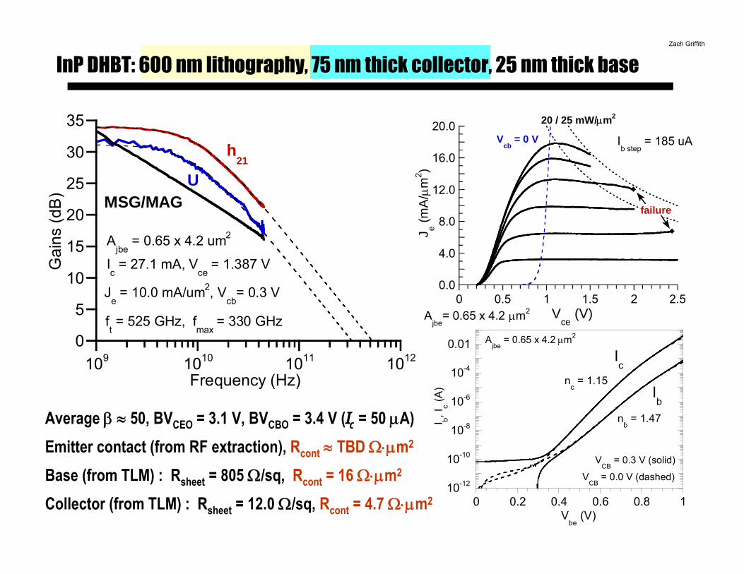
InP DHBT: 600 nm lithography, 150 nm thick collector, 30 nm thick base
Average β ≈ 36, VBR,CEO = 5.1 V (Ic = 50 μA)Emitter contact (from RF extraction), Rcont = 10.1 Ω⋅μm2
Base (from TLM) : Rsheet = 564 Ω/sq, Rcont = 9.6 Ω⋅μm2
Collector (from TLM) : Rsheet = 11.9 Ω/sq, Rcont = 5.4 Ω⋅μm2 10-12
10-10
10-8
10-6
10-4
0.01
0 0.2 0.4 0.6 0.8 1
I b, Ic (A
)
Vbe
(V)
VCB
= 0.3 V (solid)
VCB
= 0.0 V (dashed)
Ic
Ib
nc = 1.17
nb = 1.38
Ajbe
= 0.6 x 4.3 μm2
0
1
2
3
4
5
6
7
0 0.5 1 1.5 2 2.50
4
8
12
16
J e (m
A/μ
m2 )
Vce
(V)
Ajbe
= 0.6 x 4.3 μm2
Ib step
= 85 uA
Vcb
= 0 V
Ic (mA
)
Peak fτ, f
max
Ccb/Ic ~0.5 ps/V
Zach Griffith

β ≈ 40, VBR,CEO = 3.9 V. Emitter contact Rcont < 10 Ω⋅μm2
Base : Rsheet = 610 Ω/sq, Rcont = 4.6 Ω⋅μm2
Collector : Rsheet = 12.1 Ω/sq, Rcont = 8.4 Ω⋅μm2
Vcb
= -0.3 V
0
2
4
6
8
10
0 2.5 5 7.5 10 12.50
5
10
15
20
25
Ccb
/Ae (
fF/μ
m2 )
Je (mA/μm2)
Ccb (fF
)
-0.2 V
0.0 V
0.2 V
Vcb
= 0.6 V
Ajbc
= 1.3 x 6.5 μm2
Ccb
/Ic=0.2 ps/V
0.4 ps/V
0.6 ps/V
0.8 ps/V
1.0 ps/V1.5ps/V
Ajbe
= 0.6 x 4.3 μm2
Zach Griffith
0
5
10
15
20
25
30
35
109 1010 1011 1012
Gai
ns (d
B)
Frequency (Hz)
U
Ajbe
= 0.6 x 4.3 um2
Ic = 20.6 mA, V
ce = 1.53 V
Je = 8.0 mA/um2, V
cb= 0.6 V
ft = 450 GHz, f
max = 490 GHz
h21
10-12
10-10
10-8
10-6
10-4
0.01
0 0.25 0.5 0.75 1
I b, Ic (A
)
Vbe
(V)
VCB
= 0.0 V (dashed)V
CB = 0.3 V (solid)
Ic
Ib
nc = 1.12
nb = 1.41
Gummel characteristics
InP DHBT: 600 nm lithography, 120 nm thick collector, 30 nm thick base

0
5
10
15
20
25
30
35
109 1010 1011 1012
Gai
ns (d
B)
Frequency (Hz)
ft = 491 GHz, f
max = 415 GHz
U
H21
Ajbe
= 0.6 x 4.3 um2
Ic = 27.8 mA, V
ce = 1.37 V
Je = 10.3 mA/um2, V
cb= 0.4 V
MSG/MAG
Summary of device parameters—Average β ≈ 40, VBR, CEO = 3.1 V (Ic = 50 μA)Emitter contact (from RF extraction), Rcont ≈ 7.8 Ω⋅μm2
Base (from TLM) : Rsheet = 629 Ω/sq, Rcont = 6.2 Ω⋅μm2
Collector (from TLM) : Rsheet = 12.9 Ω/sq, Rcont = 4.0 Ω⋅μm2 10-12
10-10
10-8
10-6
10-4
0.01
0 0.2 0.4 0.6 0.8 1
I b, Ic (A
)
Vbe
(V)
VCB
= 0.0 V (solid)
VCB
= 0.3 V (dashed)
Ic
Ib
nc = 1.12
nb = 1.44
Ajbe
= 0.6 x 4.3 μm2
0.0
2.5
5.0
7.5
10.0
12.5
15.0
17.5
20.0
0 0.5 1 1.5 2 2.50
10
20
30
40
50
J e (m
A/μ
m2 )
Vce
(V)
Ajbe
= 0.6 x 4.3 μm2
Ib step
= 180 uA
Vcb
= 0 V
Ic (mA
)
Peak ft, f
max
Zach Griffith
InP DHBT: 600 nm lithography, 100 nm thick collector, 30 nm thick base
Average β ≈ 50, BVCEO = 3.1 V, BVCBO = 3.4 V (Ic = 50 μA)Emitter contact (from RF extraction), Rcont ≈ TBD Ω⋅μm2
Base (from TLM) : Rsheet = 805 Ω/sq, Rcont = 16 Ω⋅μm2
Collector (from TLM) : Rsheet = 12.0 Ω/sq, Rcont = 4.7 Ω⋅μm2
0
5
10
15
20
25
30
35
109 1010 1011 1012
Gai
ns (d
B)
Frequency (Hz)
ft = 525 GHz, f
max = 330 GHz
U
h21
Ajbe
= 0.65 x 4.2 um2
Ic = 27.1 mA, V
ce = 1.387 V
Je = 10.0 mA/um2, V
cb= 0.3 V
MSG/MAG
0.0
4.0
8.0
12.0
16.0
20.0
0 0.5 1 1.5 2 2.5
J e (m
A/μ
m2 )
Vce
(V)Ajbe
= 0.65 x 4.2 μm2
Ib step
= 185 uAVcb
= 0 V
20 / 25 mW/μm2
failure
10-12
10-10
10-8
10-6
10-4
0.01
0 0.2 0.4 0.6 0.8 1
I b, Ic (A
)
Vbe
(V)
VCB
= 0.3 V (solid)
VCB
= 0.0 V (dashed)
Ic
Ib
nc = 1.15
nb = 1.47
Ajbe
= 0.65 x 4.2 μm2
InP DHBT: 600 nm lithography, 75 nm thick collector, 25 nm thick baseZach Griffith

Summary of published HBT performance
)( ),/( ),/( ),/(
hence , :digital
power DCassociated gain, associated
, F:amplifiers noiselow
mW/ gain, associated
PAE, :amplifierspower
)11(
2/) (
min
1max
max
max
cb
cbb
cex
ccb
clock
ττVIRVIRIVC
f
m
ff
ff
ff
+ΔΔ
Δ
+
+
−
μ
τ
τ
τ
:metrics better
:metrics popular
0 100 200 300 400 500 600 7000
100
200
300
400
500
600
700
ft (GHz)
f max
(GH
z)
IBM SiGe
IBM SiGe
NGSTDHBT
SFUDHBT
Pohang SHBT
UCSB150 nm
500 GHz400 GHz300 GHz200 GHz
150 nm
HRLDBHT
UIUCSHBT
Updated Sept, 2005
maxffτ=
UCSB120 nm
UCSB100 nm
65 nm
75 nm
100 nm
150 nm200 nm
150 nm
RSCDHBT
120 nm
150 nm
NTTDHBT150 nm
UCSB210 nm
250 nm
100 nm
62.5nm
Fujitsu HEMTVitesse
150 nm
Stated dimensions are collector thicknessDevices are DHBTs except when labelled otherwise
UCSB75 nm
UCSB results are @ 600 nm; further progress requires scaling to 250 nm

Digital circuits: towards 200 GHz
clock rate
Z Griffith
underlying technology:400-500 GHz InP transistors
142 GHz latch from NNIN @ UCSB, 150 GHz ICs from UCSB/GSC/RSC 200 GHz is the next goal

Static Frequency Divider: Standard Digital Benchmark
ECL Master-Slave Latch with Inverting Feedback
Forms 2:1 Frequency Divider.
Maximum clock frequency is measureof technology speed.
Standard circuit configuration for consistent benchmarking - no tricks.
Small inductive peaking (L/R~1.3 ps).

+V +V +V
0V
kz
Microstrip mode Substrate modes
+V
0VCPW mode
0V 0V
CPW has parasitic modes, coupling from poor ground plane integrity
kz
Microstrip has high via inductance, has mode coupling unless substrate is thin.
We prefer (credit to NTT) thin-film microstrip wiring, inverted is best for complex ICs
-V 0V +V
0VSlot mode
ground straps suppress slot mode, but multiple ground breaks in complex ICs produce ground return inductanceground vias suppress microstrip mode, wafer thinning suppresses substrate modes
M. Urteaga, Z. Griffith, S. Krishnan
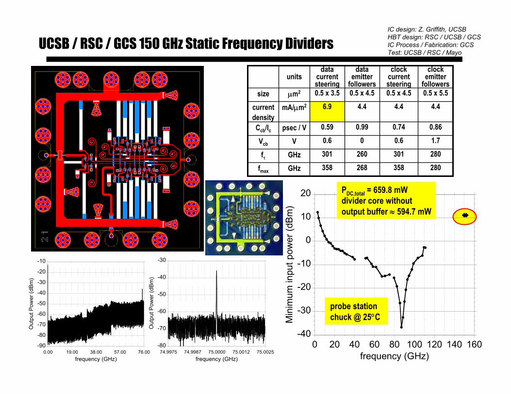
0.860.740.990.59psec / VCcb/Ic
3583010.6
4.40.5 x 4.5
clock current steering
GHzGHz
V
mA/μm2
μm2
units
280268358fmax
280260301fτ
1.700.6Vcb
4.44.46.9currentdensity
0.5 x 5.50.5 x 4.50.5 x 3.5size
clock emitter
followers
data emitter
followers
data current steering
UCSB / RSC / GCS 150 GHz Static Frequency Dividers
-40
-30
-20
-10
0
10
20
0 20 40 60 80 100 120 140 160
Min
imum
inpu
t pow
er (d
Bm
)
frequency (GHz)
IC design: Z. Griffith, UCSBHBT design: RSC / UCSB / GCSIC Process / Fabrication: GCSTest: UCSB / RSC / Mayo
-80
-70
-60
-50
-40
-30
74.9975 74.9987 75.0000 75.0012 75.0025
Out
put P
ower
(dB
m)
frequency (GHz)
-90
-80
-70
-60
-50
-40
-30
-20
-10
0.00 19.00 38.00 57.00 76.00
Out
put P
ower
(dBm
)
frequency (GHz)
probe station chuck @ 25°C
PDC,total = 659.8 mWdivider core without output buffer ≈ 594.7 mW

UCSB 142 GHz Master-Slave Latches (Static Frequency Dividers)
-90
-80
-70
-60
-50
-40
-30
-20
-10
0.0 15.0 30.0 45.0 60.0 75.0
Out
put P
ower
(dB
m)
frequency (GHz)
Static 2:1 divider:Standard digital benchmark.Master-slave latch with inverting feedback.Performance comparison between digital technologies
UCSB technology 2004:InP mesa HBT technology12-mask process600 nm emitter width142 GHz maximum clock.
Implications:160 Gb/s fiber ICs
100 + Gb/s serial links
Target is 260 GHz clock rate at 300 nm scaling generation
Z. Griffith, M. Dahlström
25o C

Reducing Digital Circuit DissipationECL with impedance-matched 50 Ohm bus:25 Ohm load→ switch 12 mA 12 mA x 7 x 4 V = 336 mW/latch
CML with impedance-matched 50 Ohm bus:25 Ohm load→ switch 12 mA 12 mA x 3 x 3 V = 108 mW/latch
Low-Power CML100 Ohm loaded → switch 3 mA 3 mA x 3 x 3 V = 27 mW/latch
Significant dissipation in the clock emitter-follower level-shifters;some published work omits this from stated dissipation
12 mA12 mA 12 mA
50 Ohm bus 50 Ohm 50 Ohm
12 mA
50 Ohm bus 50 Ohm 50 Ohm
50 Ohm bus100 Ohm
3 mA
3 mA 3 mA
padcbwiring CC ,low ,low power low @ speed High =
100 Ohm

Zach Griffith
Low Power CML Static Divider Designs

Divide-by-4 at 128.6 GHz, S3 RSC Technology
-80
-60
-40
-20
0
0 10 20 30 40 50
Out
put P
ower
(dBm
)
frequency (GHz)
Measurements performed at UCSB, GUNN Source Used For CLK InputRSC Wafer # xxxx, Divider ID: R3C2 #5A, Fabricated at RSC, Design at UCSBVclk offset = -0.45 V, VEE, div1,2 = -3.4 V, IEE, total = 192 mA – Idiv1,2 at fclk,max ≤ 65 mA per divider cktPower dissipation of input divider core w/out output buffer < 221 mW — room temp, no cooling
128.6 GHz input 5 GHz input test to prove static operation
-80
-60
-40
-20
0
0 10 20 30 40 50
Out
put P
ower
(dBm
)frequency (GHz)
Zach Griffith

Phase II divide by 2—Ultra low power CML divider47
0 μm
443 μm
Simulated divider speed…
With Collector PedestalAjbe = 1.0 μm2, fmax = 100 GHz
Pdivider core, ≈ 31 mW
Zach Griffith
Ultra Low Power CML Static Divider Design

Ultra low-power RSC / UCSB CML dividers
Output waveform @ 6.0 GHz, fclk = 12 GHz
The divider is operational from 12 GHz to 51 GHzAt fclk = 51 GHz, Pflip-flop = 29.2 mW Latch power × delay = 143 fJ, no emitter followers = 79.0 fJ
Output waveform @ 25.5 GHz, fclk = 51 GHz
-0.30
-0.25
-0.20
-0.15
-0.10
-0.05
0.00
0 125 250 375 500
Out
put S
igna
l (V)
time (ps)
Confirms the circuit is fully static
-0.30
-0.25
-0.20
-0.15
-0.10
-0.05
0.00
0 50 100 150 200
Out
put S
igna
l (V)
time (ps)
Zach Griffith

Deep Submicron Bipolar Transistors for 140-220 GHz Amplification
0
10
20
30
40
10 100 1000
Tran
sist
or G
ains
, dB
Frequency, GHz
U
UMSG/MAG
H21
unbounded U
-4
-2
0
2
4
6
8
140 150 160 170 180 190 200 210 220
S21
, dB
Frequency, GHz
1-transistor amplifier: 6.3dB @ 175 GHz
-30
-20
-10
0
10
140 150 160 170 180 190 200 210 220
gain
, dB
Frequency (GHz)
3-transistor amplifier: 8 dB @ 195 GHz
raw 0.3 μm transistor: high power gain @ 200 GHz
M. Urteaga

7.5 mW output power
Mesa DHBT Power Amplifiers for 100-200 GHz Communications
7 dB gain measured @ 175 GHz
175 GHz Power Amplifier Demonstrated in a 300 GHz fmax process500 GHz fmax DHBTs available now, 600 GHz should be feasible soon
→ feasibility of power amplifiers to 350 GHz→ Ultra high frequency communications
2 fingers x 0.8 um x 12 um, ~250 GHz fτ, 300 GHz fmax , Vbr ~ 7V, ~ 3 mA/um2 current density
V. Paidi, Z. Griffith, M. Dahlström

Common-Base Has Highest Gain, but Layout Parasitics Matter !
0
5
10
15
20
25
10 100
MSG
/MAG
F requency, G Hz
W ithou t Cce
, Lb
W ith Cce
W ith Cce
and Lb
base plug
emitter
semi-insulating InPN+ subcollector
N- collector
base
collector
N+ subcollector
Lb
CceCce
base
interconnect metal
0
5
10
15
20
25
30
10 100
MS
G/M
AG, d
B
Frequency, GHz
Common base
Common Collector
Common emitter
U ignores layout parasitics
V. Paidi, Z. Griffith, M. Dahlström

Single-Sided Collector Contacts Improve Common-Base Gain
base plug
emitter
semi-insulating InPN+ subcollector
N- collector
base
collector
N+ subcollector
Lb
base
interconnect metal
0
5
10
15
20
25
30
10 100
MSG
/MA
G
Frequency, GHz
Single sided collector
Double sided collector
amplifier designs
V. Paidi, Z. Griffith, M. Dahlström

172 GHz Common-Base Power Amplifier
8.3 dBm saturated output power 4.5-dB associated power gain at 172 GHz DC bias: Ic=47 mA, Vcb=2.1V.
-10
-5
0
5
10
140 150 160 170 180 190
S 21,S
11,S
22, d
B
Frequency, GHz
S11
S22
S21
RLVin Vout
Input Matching Network Output Loadline Match
-10
-5
0
5
10
15
0
1
2
3
4
5
-15 -10 -5 0 5
Gai
n, d
B, O
utpu
t Pow
er, d
Bm
PAE (%
)
Input Power, dBm
Gain
Output Power
PAE
V. Paidi, Z. Griffith, M. Dahlström
6 dB gain

176 GHz Two-Stage Amplifier7-dB gain at 176 GHz8.1 dBm output power, 6.3 dB power gain at 176 GHz9.1 dBm saturated output power at 176 GHz
-10
-5
0
5
10
15
140 150 160 170 180 190 200
S 21, S
11, S
22 d
B
Frequency, GHz
S21
S11
S22
0
2
4
6
8
10
0
1
2
3
4
5
-6 -4 -2 0 2 4 6 8 10
Gai
n, d
B, O
utpu
t Pow
er ,
dBm
PAE (%
)
Input Power, dBm
PAEGain
Output Power
RLVoutVin
50 Ohms 50 Ohms
InputMatchingNetwork
OutputLoadlineMatchingNetwork
InputMatchingNetwork
OutputLoadlineMatchingNetwork
λ/4 at f0
λ/4 at f0
Veb,bias
Vcb,bias
V. Paidi, Z. Griffith, M. Dahlström

Transistor ICs → compact sub-mm-wave systems
Compact, Single-Chip Monolithic Frequency Multiplier Chains
Frequencydoubler
Frequencydoubler
100 GHz400 GHz50 mW ?
200 GHz100 mW
Frequencydoubler
800 GHz10 mW ?
Sub-mm-wave Frequency Generation by phase-locked source
600 GHz
300 GHzpush-pushVCO
Gilbert-cellharmonic mixer
15 GHzreference
150 GHz
300 GHz poweramplifier
HBTactivefrequencydoubler
static ordynamicfrequencydivider75 GHz

Today: InP DHBTs @ 500 nm Scaling Generation
Device Performance:~ 400 GHz fτ and ~500 GHz fmax
Has enabled 150 GHz digital clock rate (static dividers)
Should enable 300 GHz power amplifiers (175 GHz realized with 300 GHz fmax)
InGaAs base
BC grade
collector
N+ sub collector
S.I. InP substrate
emitter
emitter contact
base contact
N- drift collector
emitter: 500 nm width, 15 Ω⋅μm2 contact resistivity
base contact: 300 nm width, 20 Ω⋅μm2 contact resistivity
collector: 150 nm thick, 5 mA/μm2 current density10 mW/μm2 power density @ 2V15 K/(mW/μm2) thermal resistance

Next: 250 nm Scaling Generation, 1.414:1 fasterGoals: 500 GHz fτ and 700 GHz fmax
230 GHz digital clock rate (static dividers)400 GHz power amplifiers
InGaAs base
BC grade
collector
N+ sub collector
S.I. InP substrate
emitter
emitter contact
base contact
N- drift collector
emitter: 250 nm width7.5 Ω⋅μm2 contact resistivity base contact:
150 nm width, 10 Ω⋅μm2 resistivity
collector: 110 nm thick, 10 mA/μm2 current density20 mW/μm2 power density @ 2V7.5 K/(mW/μm2) thermal resistance
Direct, brute-force scaling
Requires innovations in emitter & base contacts: processes & metallurgy
extrinsic base
intrinsic base
drift collector
N+ sub collector
S.I. InP substrate
pedestal
current-block layer
regrown emitter
emitter contact
base contact
Parasitic Reduction
regrown emitter with wide contact: reduces access resistance
collector pedestal: reduces capacitance under base contacts,allows wider & more resistive base contacts
Requires implants and regrowth processes
-2.00
0.00
2.00
4.00
6.00
8.00
10.00
12.00
14.00
16.00
18.00
0.00 0.50 1.00 1.50 2.00 2.50
Vce (V)
Ic (m
A)
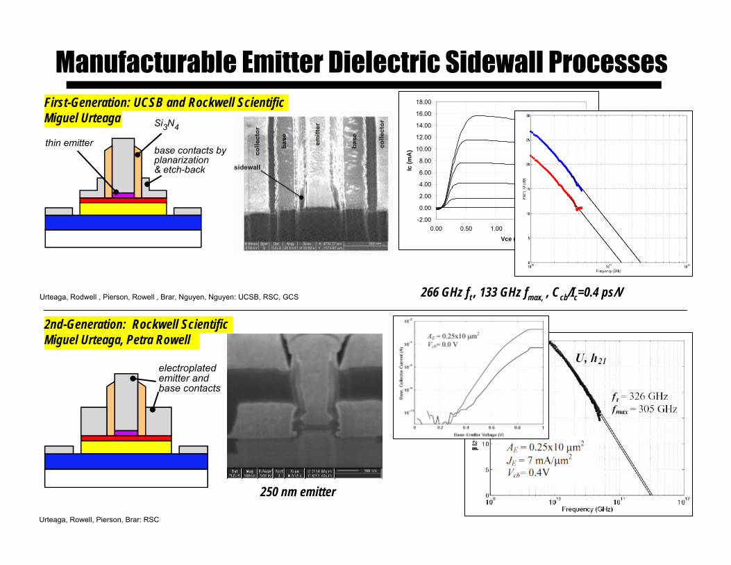
Manufacturable Emitter Dielectric Sidewall ProcessesFirst-Generation: UCSB and Rockwell Scientific Miguel Urteaga
266 GHz ft , 133 GHz fmax, , Ccb/Ic=0.4 ps/V
Si3N4
thin emitterbase contacts byplanarization& etch-back
Urteaga, Rodwell , Pierson, Rowell , Brar, Nguyen, Nguyen: UCSB, RSC, GCS
electroplatedemitter andbase contacts
2nd-Generation: Rockwell Scientific Miguel Urteaga, Petra Rowell
Urteaga, Rowell, Pierson, Brar: RSC
250 nm emitter

HBT with Epitaxial Extrinsic Emitter C. Kadow
0
1 0
2 0
3 0
4 0
0 0 .5 1 1 .5 2 2 .5 30 .0 0
0 .2 0
0 .4 0
0 .6 0
0 .8 0
1 .0 0
I c [mA
]
Vce
[V ]
Ib , s te p
= 2 m A
Jc [m
A/um2]
10-7
10-6
10-5
10-4
10-3
10-2
10-1
0 0.5 1 1.5
I b, Ic [A
]
Vbe
[V]
Voffset
= 0.0 V
IC
IB
Max( β ) = 7.0WE = 1.0 µm

Subcollector & Pedestal Implant Navin Parthasarathy
Fe
N+S.I.
N+
Epitaxial growth JunctionFabrication
N+ N+FeFe
N+S.I.
N+N+ N+Fe
Pedestal Implant
Fe
N+S.I.
N+N+ N+Fe
Fe Implant
S.I.
Fe
Subcollector Implant
N+S.I.
Fe
collector contact
pedestal implantsubcollector implantbase metal
emitter
Subcollector implant eliminates Ccbin base pad area -key for high speed in lower-power logic.Pedestal further reduces Ccb.
0
5
10
15
20
25
30
35
109 1010 1011 1012
Gai
ns (d
B)
Frequency (Hz)
ft = 352 GHz, f
max = 365 GHz
U
h21
Ajbe
= 0.65 x 4.3 μm2
Ic = 13.95 mA, V
ce = 1.834 V
Je = 5.0 mA/μm2, V
cb ~ 0.6 V
U
0.0
2.0
4.0
6.0
8.0
10.0
0 0.5 1 1.5 2 2.5 3 3.50
5
10
15
20
25
J e (m
A/μ
m2 )
Vce
(V)
Ajbe
= 0.65 x 4.3 μm2
Ib step
= 100 uA
Vcb
= 0 V
Ic (mA
)
failure
0
2
4
6
8
10
12
0 2 4 6 8 100
0.51
1.52
2.53
3.54
Ccb /A
e (fF/um
2)
Je (mA/μm2)
Ccb
(fF
)
Vcb
= 0.6 V
26% Ccb
reduction -- 28% predicted
Ajbc
~ 1.3 x 8.5 μm2
sub-collector implanted
sub-collector grown
sub-collector w/ pedestal
10-12
10-10
10-8
10-6
10-4
0.01
0 0.2 0.4 0.6 0.8 1I b, I
c (A)
Vbe
(V)
VCB
= 0.3 V (solid)
VCB
= 0.0 V (dashed)
Ic
nc = 1.18
Ajbe
= 0.65 x 4.3 μm2
Ib
50 pA
nb = 1.53

Roadmap for the 125 nm Scaling Generation
Target transistor performance: 700 GHz fτ , 1100 GHz fmax , comparable improvement of other key parameters: CcbΔV/Ic, RexIc /ΔV, RbbIc/ΔV
Target circuit performance330 GHz digital clock rate (static dividers)600 GHz power amplifiers
What would be needed to obtain this ?
InGaAs base
BC grade
collector
N+ sub collector
S.I. InP substrate
emitter
emitter contact
base contact
N- drift collector
emitter: 125 nm width, 5 Ω⋅μm2 contact resistivity
base contact: 75 nm width, ~5 Ω⋅μm2 contact resistivity
collector: 75 nm thick, 20 mA/μm2 current density40 mW/μm2 power density @ 2V4 K/(mW/μm2) thermal resistance

Indium Phosphide HBTs for 100-600 GHz ICs
InP HBT now: at 500 nm scaling generation 455 GHz ft & 485 GHz fmax150 GHz static dividers & 180 GHz amplifiers demonstrated200 GHz digital latches & 300 GHz amplifiers are feasible
InP HBT: future, at 125 nm scaling generation2:1 increase in bandwidth (?)700 GHz ft & 1.1 THz fmax , 330 GHz digital latches & 600 GHz amplifiers ?demands 4:1 better Ohmic contactsdemands 4:1 increased current density.
Applications:160+ Gb/s fiber ICs, 300 GHz MIMICs for communications, radar, & imagingGHz ADCs / DACs / DDFS / etc.& applications unforeseen & unanticipated


Submicron diodes for sub-millimeter-waves

Hierarchy of ECL Static Frequency Divider
Zo
ECL NAND/NOR Gate Level Shifters Logic Gate Core Level Shifters
C
D Q
ECL Latch: level-clocked memory element
Master-Slave Latch: transition-clocked memory element
Q
Q
D
C
Q
Q
D
C
Q
Q
DC
Q
Q
D
C
2:1 Static Frequency Divider
Q
Q
DC

Transit time Modulation Causes Ccb Modulation
( ) ),(//1)(constant0 cbccbc
T
celectronsbase
holesbase VIfTAVdxTxAxqnQQ c =+−++= ∫ ε
cb
f
c
cb
c
holesbasef
cb
holesbasecb VI
CI
QV
QC∂∂
−=∂
∂⇒
∂∂
≡∂
∂−≡
ττ
Camnitz and Moll, Betser & Ritter, D. Root holesbaseb ΔQI ,
E
drift collectorbase
-
+
+
+
+
-
-
-
--
-
-
-2
-1
0
1
2
0 100 200 300 400
eV
nm
ΓL
-2
-1
0
1
2
0 100 200 300 400
eV
nm
0 0 <∂∂⇒>∂∂ ccbcbf ICVτ :Modulation Velocity Collector
0 0 >∂∂⇒<∂∂ ccbcbf ICVτ : Effect Kirk
2
3
4
5
6
7
8
0 2.5 5 7.5 10 12.5
Ccb
/Ae (
fF/μ
m2 )
Je (mA/μm2)
-0.2 V
0.0 V
0.2 V
Vcb
= 0.6 Vcbb
cb
Vτ
C
by of modulation and- collector into pushout base-
both to due is in Increase
100
200
300
400
500
0 2 4 6 8 10 12
f τ (GH
z)
Je (mA/um2)
fτ, -0.3 V
cb
0.0 Vcb
-0.2 Vcb
0.2 Vcb
0.6 Vcb
DHBTs InP in effect weak- SHBTs InGaAs in effect strong-
reduced with in Increase cbcbc CVτ →

Transit time Modulation → Negative Resistance → Infinite Gain
electrondensity
time
collectorcurrent
collectorvoltage
Je/V0
Je/(V0+ΔV)
ΔV is negative
ΔJ=Je(ΔV/ V0)
time
(V0+ΔV)
ΔT=2τc
(V0+ΔV)
-
-
- -
-
subcollector
E
subcollector
-
-
--
--
-- -
-- - -
V0
base
M. Urteaga
( )cbfccanccb VIC ∂∂−= /ecapacitanc negative
, τ
)3/(2resistance negative
,canccbc CR τ=
econductanc negativeG positive 12
= econductanc negativeG negative 22
=