input capure em microelectronic - marin sa em6819fx …
TRANSCRIPT

EM6819Fx-A00x, EM6819Fx-A10x EM6819Fx-B00x, EM6819Fx-B10x
Copyright 2018, EM Microelectronic-Marin SA 6819-DS, Version 9.5, 3-Dec-18
1 www.emmicroelectronic.com
Sub-1V (0.6V) 8bit Flash MCU DC-DC Converter, E2PROM
Description The EM6819 is designed to be battery operated for extended lifetime applications. Its large voltage range from 3.6V down to 0.9V makes it a perfect match for today’s demanding applications. Brownout and powercheck functions ensure reliable operation at or near undervoltage conditions, offering greater reliability in complex operation modes. Each of the 24 I/Os are freely programmable and the microcontroller has a dual quartz and trimmable RC oscillator up to 15MHz. It has an 8-bit RISC architecture specially designed for very low power consumption. With 2 clocks per instruction, the EM6819 executes up to 7.5 MIPS at 15MHz and achieves astonishing 4000 MIPS/Watt.
Features Wide supply voltage range 0.9 V – 3.6 V Runs down to 0.6V with enabled DCDC and still 10mA
load current True low current: typ 140uA at 3V, 1 MIPS Up to 7.5 MIPS at 15MHz DC-DC converter using just external coil and capacitor On-chip brownout detection PowerCheck functions at start-up 32 Voltage Level Detection on Supply or Input pin 3 terminal Operational Amplifier / Comparator ADC 10-bit, 8 channel Temperature sensor Voltage reference input/output Fast wake-up Up to 24 fully configurable I/Os Flash read monitoring system lowest voltages Dual clock mode, quartz and RC oscillators:
o 2 MHz – 15MHz RC, pre-trimmed o Low freq RC Oscillator (8kHz) o 32768 Hz Xtal, 4MHz Resonator/Xtal, Ext Clock
8-bit CoolRISC architecture o 16 registers o 8*8bit hardware multiplier
Power-On-Reset and watchdog GPNVM Memory
o Sharing Instruction code and data Fully static 512 Byte RAM Internal and external interrupts Frequency generator 4 independent PWM outputs 8/16-bit timers Prescaler for RC and XTAL SPI interface Small size, Green mold / lead-free packages
Tools & Services On chip debug system in the application ISP (In-system) programming C-compiler Windows-based software programs Programmer from different vendors Dedicated team of engineers for outstanding support
Architecture
Power Supply
0.9 – 3.6V
DC-DC Up-Converter
2.1V, 2.5V, 2.9V, 3.3V
Voltage Regulator
Power On
Reset
BrownOut
&
Power Check
Voltage Level
Detector
32 – levels
VSUP, PA, PC
GPNVM (FLASH)
16.9 kByte
Data Instruction
Memory Memory
Max 12 kB Max 6 kInstr
Reset &
wake-up
Controller
RC 8KHz
Watch Dog
IRQ & Event
controller
Crystal 32kHz
Prescaler 210 stages
Prescaler 115 stages for
RTC
GASP
Debug-on-Chip
ISP
Monitor
2 wire & TM
Timer1,
Timer2
2x8 bit or 16 bit
PWM , Freq Gen
Input capure
Output compare
ADC 10 BIT
8 channels
OPERTIONAL
AMPLIFIER
3 terminals,
PA, PC
8 BITS PORT A
Pull-up, pull-down
Interrupt, Capture
Reset & Wake-up
ADC, VLD, OPA,VREF
Timer start & clock
PWM, Signals
8 BITS PORT B
SPI or soft UART
PWM, signals
GASP interface
POWER
MANAGEMENT
&
SECURITY
MEMORIES
&
CORE
Digital
&
Analog
PERIPHERALS
CLOCK
&
SYSTEM
8 BITS PORT C
Pull-up, pull-down
Interrupt,Capture
ADC, VLD, OPA
Timer start & clock
PWM, Signals
Crystal or
Resonator4MHz
X1(optional)
RC 2 MHz
RC 15 MHz32kHz /
4MHz
Sleep
Counter
wake-up
Timer3,
Timer4
2x8 bit or 16 bit
PWM , Freq Gen
Input capure
Output compare
IO’s
RAM
512 BytesFully static
CoolRISC 8-bitsCR816L
16 registers
HW multiplier
ROM-API
Application
subroutines
PA[7:0] PB[5:0]PC[7:0] PB[7:6] TM
Temp
Sensor
SPI
8 bits
master or
slave
+
DC-DC
VREG
Cvreg
VSUP
Cdcdc
VSS
VSSDC
VSS2
VSUP2
Ldcdc
Pinout for 32 lead QFN Others include SO8, TSSOP16/20/28, and QFN20/32
32 31 30 29 28 27 26 25
2
1
9 10 11 12 13 14 15 16
PB7
PA0
PC0
PA1
PC1
PA2
PC2
PA3
DCDC
VSUP2
VSUP
PB1
PB0
PC7
PA7
PA6
PB
6
PB
5
PB
4
PB
3
PB
2
VS
S
2 VS
S
VS
S_
DC
-DC
PC
3
VR
EG
PA
4
PC
4
TM
PA
5
PC
5
PC
6
4
3
6
5
8
7
23
24
21
22
19
20
17
18
32 Lead QFN
5x5mm body
EM6819
DCDC
Typical Applications Metering Safety and Security devices Heat Cost Allocation Sensor Interfaces, Smoke detector Security Body care Sports Computer peripherals, Bluetooth chipset Wireless
EM MICROELECTRONIC - MARIN SA

EM6819Fx-A00x, EM6819Fx-A10x EM6819Fx-B00x, EM6819Fx-B10x
Copyright 2018, EM Microelectronic-Marin SA 6819-DS, Version 9.5, 3-Dec-18
2 www.emmicroelectronic.com
Power supply - Low power architecture - Voltage regulator for internal logic supply - External regulator capacitor - Voltage mult: gives internal multiplied voltage to allow
0.9V start-up (Padring remains on VSUP) - DC-DC Upconverter: with ext Coil and Cap. Increases
the VSUP for the whole circuit I.e to 3V. Running down to 0.6V input voltage.
CPU - 8-bit CoolRisc 816L Core - 16 internal registers - 4 hardware subroutine stacks - 8-bit hardware multiplier
Flash/EEPROM - 16.9k Byte shared Genaral Purpose Non Volatile Flash
memory - max 6k Instructions program memory - max 12 kByte non volatile data memory
RAM - 512 x 8-bit static SRAM - 48 byte of Ram-cache for EEProm modification support
Operating modes - Active mode: CPU and peripherals are running - Standby mode: CPU halted, peripherals on - Sleep mode: no clocks, data retained - Power-Down mode, Reset state - Wake Up Event from PortA inputs
Resets - Power On Reset - Reset from logic watchdog - Brown out (as voltage supervisory function) - Reset with Port A selection - Flags to identify the reset source
Watchdog timer - generation of watchdog reset after time out - independent low frequency watchdog oscillator
Oscillator RC - internal RC oscillator, 2MHz and 15MHz pre-trimmed - internal 8 KHz RC Oscillator
External Oscillator - 32 KHz watch type Crystal or 4MHz Resonator/XTAL
Prescaler’s - Two clock prescalers (dividers) for the peripheral clock
generation: - Prescaler 1 is a 15-stage divider - Prescaler 2 is a 10-stage divider
- input clock software selectable - fix intervall IRQ’s
Interrupt - external IRQ’s from Port A, VLD, Comparator - internal IRQ’s from Timer, Prescaler, ADC, SPI - Event from SPI/ADC and DoC
VLD - Detection of 32 voltage levels, internal reference - Comparison against VSUP, input Pin or Op.Amp output
Parallel In/Output Port A, Port C - 8-bit wide direct input read - all functions bit-wise configurable
- Input , output - Debouncer, IRQ on pos. or neg. edge - Input combination reset - Pullup, pulldown or nopull selectable - Freq. Input for timer - Analog In/Out
Parallel In/Output Port B - 8 multipurpose I/O’s - 8-bit wide direct input read - CMOS or Nch. Open Drain outputs - all functions bit-wise configurable
- Input , output - Pullup, pulldown or nopull selectable - CMOS or Nch. Open Drain outputs
Serial Port Interface SPI - 3 wire serial Interface, Sclk, Sin, Sout - master and Slave mode - Serial datastream output - Event / IRQ - Maped on port outputs
Timer (4 x 8-bit, or 2 x 16-bit) - 8 (16) bit wide, Zero Stop and Auto Reload mode - External signal pulse width measurement - PWM generation, IRQ - Event Counter - Input capture - Output compare
Sleep Counter Wake-up (SCWUP) - Automatically wakes up the circuit from sleep mode - Enable/disable by register
Op. Amplifier / Comparator - All 3 terminals mapped on PortA/PortC - Output routed to VLD cell - Amplifier or Comparator output
Temp. Sensor - Fully internal temperature sensor - Multiplexed input to ADC
Brown Out - On-chip Brown-Out detection, reset state - Power check at Startup
ADC - 10-bit, 8 channels ADC - Single or Continuous mode - External/internal reference voltage available on a pad - Event / IRQ
DoC (Debug on Chip) - 2 wire serial interface debug and programming interface - Flash programming - Event / IRQ

EM6819Fx-A00x, EM6819Fx-A10x EM6819Fx-B00x, EM6819Fx-B10x
Copyright 2018, EM Microelectronic-Marin SA 6819-DS, Version 9.5, 3-Dec-18
3 www.emmicroelectronic.com
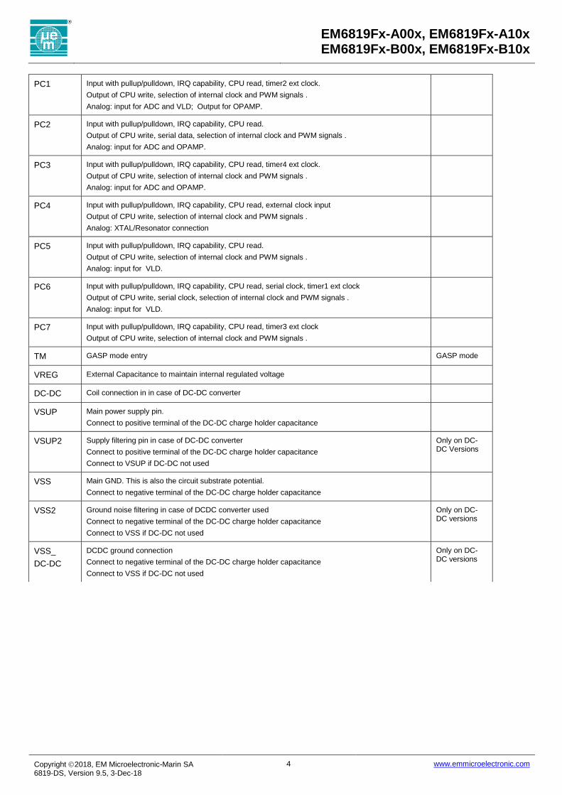
Pin Name Software selectable functions Remarks
PA0 Input with pullup/pulldown, IRQ capability, CPU read, wake-up, timer1 ext clock.
Output of CPU write and a selection of internal clock and PWM signals.
Analog input for ADC.
PA1 Input with pullup/pulldown, IRQ capability, CPU read, wake-up, timer2 ext clock.
Output of CPU write, selection of internal clock and PWM signals .
Analog: input for ADC and VLD; Output for OPAMP.
PA2 Input with pullup/pulldown, IRQ capability, CPU read, wake-up, serial data input, timer3 ext clock.
Output of CPU write, serial data out and selection of internal clock and PWM signals
Analog: input for ADC,VLD and Opamp;
PA3 Input with pullup/pulldown, IRQ capability, CPU read, wake-up, serial data input, timer4 ext clock.
Output of CPU write, serial data out and selection of internal clock and PWM signals
Analog: input for ADC,VLD and Opamp;
PA4 Input with pullup/pulldown, IRQ capability, CPU read, wake-up, serial data.
Output of CPU write and a selection of internal clock and PWM signals.
Analog: XTAL/Resonator connection.
PA5 Input with pullup/pulldown, IRQ capability, CPU read, wake-up.
Output of CPU write and a selection of internal clock and PWM signals.
PA6 Input with pullup/pulldown, IRQ capability, CPU read, wake-up, serial clock..
Output of CPU write, serial clock and a selection of internal clock and PWM signals.
Analog: input for VLD ; Output for VBGP
PA7 Input with pullup/pulldown, IRQ capability, CPU read, wake-up, serial clock..
Output of CPU write, serial data and a selection of internal clock and PWM signals.
Analog: input for VLD ; Output for internal reference voltage
PB0 Input with pullup/pulldown, CPU read, serial data.
Output of CPU write and a selection of internal clock and PWM signals.
PB1 Input with pullup/pulldown, CPU read.
Output of CPU write and a selection of internal clock and PWM signals.
PB2 Input with pullup/pulldown, CPU read, serial clock.
Output of CPU write, serial clock and a selection of internal clock and PWM signals.
PB3 Input with pullup/pulldown, CPU read.
Output of CPU write and a selection of internal clock and PWM signals.
PB4 Input with pullup/pulldown, CPU read.
Output of CPU write, serial data and a selection of internal clock and PWM signals.
PB5 Input with pullup/pulldown, CPU read.
Output of CPU write and a selection of internal clock and PWM signals.
PB6 Input with pullup/pulldown, CPU read.
Output of CPU write and a selection of internal clock and PWM signals.
GASP clock
PB7 Input with pullup/pulldown, CPU read.
Output of CPU write and a selection of internal clock and PWM signals.
GASP data
PC0
Input with pullup/pulldown, IRQ capability, CPU read, timer1 ext clock.
Output of CPU write and a selection of internal clock and PWM signals.
Analog input for ADC.
EM6819Fx-A00x, EM6819Fx-A10x EM6819Fx-B00x, EM6819Fx-B10x
Copyright 2018, EM Microelectronic-Marin SA 6819-DS, Version 9.5, 3-Dec-18
4 www.emmicroelectronic.com
PC1 Input with pullup/pulldown, IRQ capability, CPU read, timer2 ext clock.
Output of CPU write, selection of internal clock and PWM signals .
Analog: input for ADC and VLD; Output for OPAMP.
PC2 Input with pullup/pulldown, IRQ capability, CPU read.
Output of CPU write, serial data, selection of internal clock and PWM signals .
Analog: input for ADC and OPAMP.
PC3 Input with pullup/pulldown, IRQ capability, CPU read, timer4 ext clock.
Output of CPU write, selection of internal clock and PWM signals .
Analog: input for ADC and OPAMP.
PC4 Input with pullup/pulldown, IRQ capability, CPU read, external clock input
Output of CPU write, selection of internal clock and PWM signals .
Analog: XTAL/Resonator connection
PC5 Input with pullup/pulldown, IRQ capability, CPU read.
Output of CPU write, selection of internal clock and PWM signals .
Analog: input for VLD.
PC6 Input with pullup/pulldown, IRQ capability, CPU read, serial clock, timer1 ext clock
Output of CPU write, serial clock, selection of internal clock and PWM signals .
Analog: input for VLD.
PC7 Input with pullup/pulldown, IRQ capability, CPU read, timer3 ext clock
Output of CPU write, selection of internal clock and PWM signals .
TM GASP mode entry GASP mode
VREG External Capacitance to maintain internal regulated voltage
DC-DC Coil connection in in case of DC-DC converter
VSUP Main power supply pin.
Connect to positive terminal of the DC-DC charge holder capacitance
VSUP2 Supply filtering pin in case of DC-DC converter
Connect to positive terminal of the DC-DC charge holder capacitance
Connect to VSUP if DC-DC not used
Only on DC-DC Versions
VSS Main GND. This is also the circuit substrate potential.
Connect to negative terminal of the DC-DC charge holder capacitance
VSS2 Ground noise filtering in case of DCDC converter used
Connect to negative terminal of the DC-DC charge holder capacitance
Connect to VSS if DC-DC not used
Only on DC-DC versions
VSS_
DC-DC
DCDC ground connection
Connect to negative terminal of the DC-DC charge holder capacitance
Connect to VSS if DC-DC not used
Only on DC-DC versions

EM6819Fx-A00x, EM6819Fx-A10x EM6819Fx-B00x, EM6819Fx-B10x
Copyright 2018, EM Microelectronic-Marin SA 6819-DS, Version 9.5, 3-Dec-18
5 www.emmicroelectronic.com
TABLE OF CONTENTS
1. EM6819 FAMILY 11
2. SYSTEM OVERVIEW 12
2.1 OPERATING MODES 13 2.1.1 Active mode 13
2.2 LOW POWER MODES 13 2.2.1 Standby mode 13 2.2.2 Sleep mode 14 2.2.3 Sleep Wake-up 14 2.2.4 Power-down mode 15 2.2.5 Operation mode registers 16
2.3 REGISTER TYPES 17 2.4 POWER MANAGEMENT 18
2.4.1 Brownout 18 2.4.2 Powercheck 18 2.4.3 POR 18 2.4.4 Power managment Registers 19
2.5 REGISTER MAP 20 2.6 PORT TERMINAL CONNECTION REFERENCE TABLE 27 2.7 TSSOP PACKAGE PINOUT CIRCUIT WITHOUT DC-DC AND S08 28 2.8 TSSOP PACKAGE PINOUT CIRCUIT WITH DC-DC 29 2.9 QFN PACKAGES WITH AND WITHOUT DCDC 30
3. CPU CORE CR816 31
3.1 PM_MISS FUNCTION (FLASH READ MONITOR) 31
4. NVM MEMORY 32
4.1 INTRODUCTION 32 4.2 NVM ARCHITECTURE 32 4.3 RAM CACHE 33 4.4 WRITE DATA IN NVM 33
4.4.1 Row and sector selection 34 4.4.2 Fast/slow operation 34 4.4.3 Erase 34 4.4.4 Write 34
4.5 ROW 61 SECTOR 5 35 4.6 ROW 62 SECTOR 5 35
4.6.1 Temperature tolerance 35 4.7 ROW 63 SECTOR 5 36 4.8 READ DATA IN NVM 37 4.9 ROW TO CACHE 37
4.9.1 NVM configuration registers 38
5. CRC CHECK 39
5.1 CRC CHECK ON PROGRAM AREA 39 5.2 CRC CHECK ON DATA AREA 39
6. ROM API ROUTINES 40
6.1 BOOT SEQUENCE 40 6.2 SUB-ROUTINES USED FOR APPLICATION 41
7. RAM 42
8. RESET CONTROLLER 43
8.1 RESET SOURCES 43 8.2 RESET SIGNALS 43
8.2.1 POR 43 8.2.2 PorLog 43 8.2.3 ResAna 43 8.2.4 ResSys 43 8.2.5 Reset Flags 44

EM6819Fx-A00x, EM6819Fx-A10x EM6819Fx-B00x, EM6819Fx-B10x
Copyright 2018, EM Microelectronic-Marin SA 6819-DS, Version 9.5, 3-Dec-18
6 www.emmicroelectronic.com
8.3 RESET REGISTERS 44
9. OSCILLATOR AND CLOCKING STRUCTURE 45
9.1 EXTERNAL CLOCK SELECTION 46 9.2 INTERNAL HIGH AND LOW FREQUENCY CLOCK SELECTION 46
9.2.1 external clock selection Restrictions 47 9.2.2 CPU Clock selection 47 9.2.3 Prescaler1 Clock selection 48 9.2.4 Prescaler 2 Clock selection 48
9.3 CLOCK CONTROL 49 9.4 OSCILLATORS CONTROL 50 9.5 CLOCK CONTROL REGISTERS 52
10. PRESCALER1 54
10.1 PRESCALER1 CLOCK SELECTION 54 10.2 PRESCALER1 RESET 55 10.3 PRESCALER REGISTERS 55
11. PRESCALER2 56
11.1 PRESCALER2 CLOCK SELECTION 56 11.2 PRESCALER2 RESET 56 11.3 PRESCALER2 REGISTERS 56
12. INTERRUPT AND EVENT CONTROLLER 57
12.1 INTERRUPTS GENERAL 57 12.1.1 Basic features 57
12.2 INTERRUPT ACQUISITION 58 12.3 INTERRUPTS FROM IO PORTS 59 12.4 INTERRUPT ACQUISITION MASKING. 59
12.4.1 Pre and Postmasking of interrupts 59 12.5 INTERRUPT ACQUISITION CLEARING 60
12.5.1 Software Interrupt acquisition set 60 12.6 INTERRUPT REGISTERS 60 12.7 EVENT GENERAL 63
12.7.1 Basic features 63 12.8 EVENT ACQUISITION 63 12.9 EVENT MASKING 64 12.10 EVENT ACQUISITION CLEARING 65 12.11 SOFTWARE EVENT SETTING 65 12.12 EVENT REGISTERS 65
13. CPU INTERRUPT AND EVENT HANDLING 66
13.1 INTERRUPT PRIORITY 66 13.2 CPU STATUS REGISTER 67 13.3 CPU STATUS REGISTER PIPELINE EXCEPTION 67 13.4 PROCESSOR VECTOR TABLE 68 13.5 CONTEXT SAVING 68
14. PORT A 69
14.1 PORT A TERMINAL MAPPING 69 14.2 PORT A IO OPERATION 69 14.3 OUTPUT SIGNALS ON PORT A 71 14.4 PORT A DEBOUNCER 72 14.5 PORT A INTERRUPT GENERATION 72
14.5.1 PA Irq in Active and Standby mode 72 14.5.2 PA Irq in Sleep Mode 72
14.6 PORT A RESET FUNCTION 72 14.7 PORT A WAKE-UP FUNCTION 72 14.8 PORT A REGISTERS 73
15. PORT B 75
15.1 PORT B TERMINAL MAPPING 75

EM6819Fx-A00x, EM6819Fx-A10x EM6819Fx-B00x, EM6819Fx-B10x
Copyright 2018, EM Microelectronic-Marin SA 6819-DS, Version 9.5, 3-Dec-18
7 www.emmicroelectronic.com
15.2 PORT B IO OPERATION 75 15.2.1 Gasp communication on PB7, PB6 76
15.3 OUTPUT SIGNALS ON PORT B 77 15.4 PORT B REGISTERS 78
16. PORT C 79
16.1 PORT C TERMINAL MAPPING 79 16.2 PORT C IO OPERATION 79 16.3 OUTPUT SIGNALS ON PORT C 81 16.4 PORT C DEBOUNCER 82 16.5 PORT C INTERRUPT GENERATION 82
16.5.1 PC Irq in Active and Standby mode 82 16.5.2 PC Irq in Sleep Mode 82
16.6 PORT C REGISTERS 83
17. TIMERS 85
17.1 TIMER CHAINING 85 17.2 TIMER CLOCK SOURCES 86 17.3 TIMER START 87
17.3.1 Software start - Stop 87 17.3.2 Hardware Start – Stop (period counting) 87 17.3.3 Hardware Start – Stop (puls counting) 88
17.4 AUTO-RELOAD MODE 89 17.5 AUTO-STOP MODE 89 17.6 TIMER INPUT CAPTURE 90 17.7 OUTPUT COMPARE 92 17.8 OUTPUT COMPARE - PWMX SIGNAL PORT MAPPING 93 17.9 TIMER INTERRUPTS 94 17.10 TIMER REGISTERS 94
18. SPI – SERIAL INTERFACE 98
18.1 SCLK - SPI MASTER/ SLAVE MODE AND CLOCK SELECTION 99 18.2 SIN PORT MAPPING 100 18.3 SOUT PORT MAPPING 100 18.4 SPI START – STOP 100 18.5 AUTO-START 100 18.6 RTZ POSITIVE EDGE TRANSMISSION 101 18.7 RTO POSITIVE EDGE TRANSMISSION 101 18.8 RTZ NEGATIVE EDGE TRANSMISSION 101 18.9 RTO NEGATIVE EDGE TRANSMISSION 102 18.10 SPI REGISTERS 102
19. WATCHDOG 103
19.1 WATCHDOG CLEAR 103 19.2 WATCHDOG DISABLING 103 19.3 WATCHDOG REGISTERS 104
20. SLEEP COUNTER WAKE-UP 105
20.1 SC WAKE-UP ENABLING 105 20.2 SC WAKE-UP DISABLING 106 20.3 SC WAKE-UP REGISTERS 107
21. 10-BITS ADC 108
21.1 CONDITIONER 108 21.1.1 Range selection 108 21.1.2 Reference selection 109 21.1.3 Analog input selection 110
21.2 ADC OFFSET TRIM SELECTION 110 21.2.1 Running mode 111 21.2.2 ADC enabling 111 21.2.3 ADC sampling rate 112 21.2.4 Low noise mode 112

EM6819Fx-A00x, EM6819Fx-A10x EM6819Fx-B00x, EM6819Fx-B10x
Copyright 2018, EM Microelectronic-Marin SA 6819-DS, Version 9.5, 3-Dec-18
8 www.emmicroelectronic.com
21.2.5 8bit ADC selection 112 21.3 ADC ACQUISITION SEQUENCE 113 21.4 ADC REGISTERS 113
22. TEMPERATURE SENSOR 114
22.1 TEMPERATURE SENSOR ENABLING 114 22.2 TEMPERATURE SENSOR REGISTERS 114
23. DC/DC CONVERTER 115
23.1 DC/DC ENABLING 115 23.2 DC/DC VOLTAGE SELECTION 115 23.3 DC/DC LOW NOISE MODE 115 23.4 DC-DC REGISTER 116
24. BAND GAP 117
24.1 BAND GAP REGISTER 117
25. VLD 118
25.1 VLD SOURCE AND LEVEL SELECTION 118 25.2 VLD ENABLE 118 25.3 VLD RESULT 118 25.4 VLD INTERRUPT 119 25.5 VLD TRIMMING 119 25.6 VLD REGISTERS 119
26. RC OSCILLATOR 120
26.1 RC OSCILLATORS REGISTERS 120
27. XTAL OSCILLATOR 32KHZ 121
28. RESONATOR 4MHZ 122
29. 8KHZ OSCILLATOR 123
30. ANALOG OPAMP 124
30.1 SELECT OPAMP/COMPARATOR 124 30.2 SUPPLY SELECTION 124 30.3 COMPARATOR RESULT 125 30.4 OPAMP REGISTERS 125
31. BLOCKS CONSUMPTION 126
32. TYPICAL T AND V DEPENDENCIES 127
32.1 IDD CURRENTS 127 32.1.1 General conditions 127
32.2 IOL AND IOH DRIVES 134 32.3 PULL-UP AND PULL-DOWN 137 32.4 RC OSCILLATOR 15MHZ AND 2MHZ 139
33. ELECTRICAL SPECIFICATION 140
33.1 ABSOLUTE MAXIMUM RATINGS 140 33.2 HANDLING PROCEDURES 140 33.3 STANDARD OPERATING CONDITIONS 140 33.4 TYPICAL 32KHZ CRYSTAL SPECIFICATION 141 33.5 TYPICAL 4MHZ CRYSTAL SPECIFICATION 141 33.6 TYPICAL 4MHZ RESONATOR SPECIFICATION 141 33.7 DC CHARACTERISTICS - POWER SUPPLY CURRENTS 142 33.8 DC CHARACTERISTICS – VOLTAGE DETECTION LEVELS 144 33.9 DC CHARACTERISTICS – REFERENCE VOLTAGE 144 33.10 DC CHARACTERISTICS – DC-DC CONVERTER 145 33.11 DC CHARACTERISTICS – OSCILLATORS 145 33.12 DC CHARACTERISTICS – VHIGH 146 33.13 DC CHARACTERISTICS – OPAMP 146 33.14 DC CHARACTERISTICS – ADC 146 33.15 DC CHARACTERISTICS – TEMPERATURE SENSOR 147

EM6819Fx-A00x, EM6819Fx-A10x EM6819Fx-B00x, EM6819Fx-B10x
Copyright 2018, EM Microelectronic-Marin SA 6819-DS, Version 9.5, 3-Dec-18
9 www.emmicroelectronic.com
33.16 DC CHARACTERISTICS - I/O PINS (ON PACKAGE) 147 33.17 DC CHARACTERISTICS - I/O PINS (ON DIE) 148
34. WAKEUP AND BOOT SEQUENCE TIMING 149
35. PACKAGE DRAWINGS 150
35.1 DIMENSIONS OF TSSOP28 PACKAGE 150 35.2 DIMENSIONS OF TSSOP24 PACKAGE 151 35.3 DIMENSIONS OF TSSOP20 PACKAGE 152 35.4 DIMENSIONS OF TSSOP16 PACKAGE 153 35.5 DIMENSIONS OF SO8 PACKAGE 154 35.6 DIMENSIONS OF QFN32 PACKAGE 155 35.7 DIMENSIONS OF QFN20 PACKAGE 156 35.8 PAD LOCATION OF THE DIE (VERSION 005 AND 006) 157 35.9 PAD LOCATION OF THE DIE (ALL OTHER VERSIONS) 158
36. PACKAGE MARKING 159
37. ERRATA 160
38. ORDERING INFORMATION 161

EM6819Fx-A00x, EM6819Fx-A10x EM6819Fx-B00x, EM6819Fx-B10x
Copyright 2018, EM Microelectronic-Marin SA 6819-DS, Version 9.5, 3-Dec-18
10 www.emmicroelectronic.com
Acronyms used in this document MSB most significant bit LSB least significant bit CR / CPU/ CoolRisc 816 CPU core NVM Non Volatile Memory ROM Read Only Memory RAM Random Access Memory API Application Program Interface GASP General Access Serial Port SW Software HW Hardware ‘1’ / H / high Determines HIGH value, logical true ‘0’ / L / low Determines LOW value, logical false POR Power on reset PWRC Power check SCWUP Sleep Counter Wake-up VLD Voltage Level Detector (T) Tested in the production (Q) Validated during qualification (D) Guaranteed by the design
Nomenclature Bit order scheme in this document is [n:0] where bit ‘n’ is the MSB and bit ‘0’ is the LSB, unless otherwise stated. Positive logic is assumed, High (‘1’) values means asserted or active state and Low (‘0’) value means not asserted or inactive state, unless otherwise stated. Register names and register bit names are written in bold typeface. Signal names are written in italic-bold type face. API subroutines are written in italic
Naming convention The XTAL frequency is 32.768 kHz but is this document it is written 32 KHz (k=1000, K=1024).
Related Documents [1] CoolRISC 816L 8-bit Microprocessor Core, Hardware und Software Reference Manual V1.1 Mai 2002 [2] ROM API document

EM6819Fx-A00x, EM6819Fx-A10x EM6819Fx-B00x, EM6819Fx-B10x
Copyright 2018, EM Microelectronic-Marin SA 6819-DS, Version 9.5, 3-Dec-18
11 www.emmicroelectronic.com
EM
68
19
fa
mil
y e
ns
ure
s 0
.9V
ba
tte
ry o
pe
rati
on
s a
nd
mu
ch
mo
re …
Pa
rt n
um
be
r
Flash
code
(KW
ords)
max
NV
M d
ata
(KB
)
RA
M (B
) Supply
range
(V) D
CD
C c
onvert
or
GP
IOs
pins
Dig
ital c
omm
unicat
ion
Clo
ck s
peed
Inte
rnal
osc
illat
or
8bit
Timer
sP
WM
(up to
chan
nel)
10bit
AD
C (u
p to c
hannel
)
Temp. S
enso
r
Additi
onal a
nalog
Additi
onal d
igita
lse
lf w
rite
for
softw
are
update
Deb
ug On C
hip /
ISP
Pac
kage(
s)
Note
1
2K word Flash
(5.6kByte)
EM
68
19
F2
-B0
06
24
256
0.9
- 3
.6 -
04 to 1
2
SP
I
SW
-UA
RT
/ I2
C1
5M
Hz
RC
8kH
z 2
MH
z 1
5M
Hz
44
- -
Pw
rCk B
row
n-O
ut
VL
D
SC
WU
P
WD
SO
08
TS
SO
P1
6
EM
68
19
F2
-B0
00
24
512
0.9
- 3
.6 -
12 to 2
4
SP
I
SW
-UA
RT
/ I2
C1
5M
Hz
RC
8kH
z 2
MH
z 1
5M
Hz
Cry
sta
l 3
2kH
z -
4M
hz
44
8
Pw
rCk B
row
n-O
ut
OP
AM
P V
LD
SC
WU
P
WD
TS
SO
P1
6-2
0-2
8
QF
N2
0
EM
68
19
F2
-A0
00
24
512
0.9
- 3
.6
12 to 2
0
SP
I
SW
-UA
RT
/ I2
C1
5M
Hz
RC
8kH
z 2
MH
z 1
5M
Hz
Cry
sta
l 3
2kH
z -
4M
hz
44
8
Pw
rCk B
row
n-O
ut
OP
AM
P V
LD
SC
WU
P
WD
TS
SO
P2
0-2
8
QF
N2
0
EM
68
19
F2
-B3
00
24
512
1.8
- 5
.5 -
16 to 2
4
SP
I
SW
-UA
RT
/ I2
C1
5M
Hz
RC
8kH
z 2
MH
z 1
5M
Hz
Cry
sta
l 3
2kH
z -
4M
hz
44
8
Pw
rCk B
row
n-O
ut
OP
AM
P V
LD
SC
WU
P
WD
TS
SO
P2
0-2
8
QF
N2
0
EM
68
19
F4
-B0
05
48
256
0.9
- 3
.6 -
04 to 1
2
SP
I
SW
-UA
RT
/ I2
C1
5M
Hz
RC
8kH
z 2
MH
z 1
5M
Hz
44
4 -
Pw
rCk B
row
n-O
ut
OP
AM
P V
LD
SC
WU
P
WD
SO
08
TS
SO
P1
6
EM
68
19
F4
-A0
05
48
256
0.9
- 3
.6
08 to 1
2
SP
I
SW
-UA
RT
/ I2
C1
5M
Hz
RC
8kH
z 2
MH
z 1
5M
Hz
44
4 -
Pw
rCk B
row
n-O
ut
OP
AM
P V
LD
SC
WU
P
WD
TS
SO
P1
6-2
0
QF
N2
0
EM
68
19
F4
-A0
00
48
512
0.9
- 3
.6
12 to 2
4
SP
I
SW
-UA
RT
/ I2
C1
5M
Hz
RC
8kH
z 2
MH
z 1
5M
Hz
Cry
sta
l 3
2kH
z -
4M
hz
44
8
Pw
rCk B
row
n-O
ut
OP
AM
P V
LD
SC
WU
P
WD
TS
SO
P2
0-2
8
QF
N2
0-3
2
EM
68
19
F4
-B0
00
48
512
0.9
- 3
.6 -
12 to 2
4
SP
I
SW
-UA
RT
/ I2
C1
5M
Hz
RC
8kH
z 2
MH
z 1
5M
Hz
Cry
sta
l 3
2kH
z -
4M
hz
44
8
Pw
rCk B
row
n-O
ut
OP
AM
P V
LD
SC
WU
P
WD
TS
SO
P1
6-2
0-2
8
QF
N2
0
EM
68
19
F4
-B1
00
48
512
1.8
- 3
.6-
12 to 2
4
SP
I
SW
-UA
RT
/ I2
C1
5M
Hz
RC
8kH
z 2
MH
z 1
5M
Hz
Cry
sta
l 3
2kH
z -
4M
hz
44
8
Pw
rCk B
row
n-O
ut
OP
AM
P V
LD
SC
WU
P
WD
TS
SO
P1
6-2
0-2
8
QF
N2
0
EM
68
19
F4
-B3
00
48
512
1.8
- 5
.5 -
16 to 2
4
SP
I
SW
-UA
RT
/ I2
C1
5M
Hz
RC
8kH
z 2
MH
z 1
5M
Hz
Cry
sta
l 3
2kH
z -
4M
hz
44
8
Pw
rCk B
row
n-O
ut
OP
AM
P V
LD
SC
WU
P
WD
TS
SO
P2
0-2
8
QF
N2
0
EM
68
19
F6
-B0
04
612
512
0.9
- 3
.6 -
04 to 2
4
SP
I
SW
-UA
RT
/ I2
C1
5M
Hz
RC
8kH
z 2
MH
z 1
5M
Hz
44
8
Pw
rCk B
row
n-O
ut
OP
AM
P V
LD
SC
WU
P
WD
SO
08
TS
SO
P1
6-2
0-2
8
EM
68
19
F6
-A0
00
612
512
0.9
- 3
.6
12 to 2
4
SP
I
SW
-UA
RT
/ I2
C1
5M
Hz
RC
8kH
z 2
MH
z 1
5M
Hz
Cry
sta
l 3
2kH
z -
4M
hz
44
8
Pw
rCk B
row
n-O
ut
OP
AM
P V
LD
SC
WU
P
WD
TS
SO
P2
0-2
8
QF
N2
0-3
2
EM
68
19
F6
-B1
00
612
512
1.8
- 3
.6 -
12 to 2
4
SP
I
SW
-UA
RT
/ I2
C1
5M
Hz
RC
8kH
z 2
MH
z 1
5M
Hz
Cry
sta
l 3
2kH
z -
4M
hz
44
8
Pw
rCk B
row
n-O
ut
OP
AM
P V
LD
SC
WU
P
WD
TS
SO
P1
6-2
0-2
8
QF
N2
0
EM
68
19
F6
-A1
00
612
512
1.8
- 3
.6
12 to 2
4
SP
I
SW
-UA
RT
/ I2
C1
5M
Hz
RC
8kH
z 2
MH
z 1
5M
Hz
Cry
sta
l 3
2kH
z -
4M
hz
44
8
Pw
rCk B
row
n-O
ut
OP
AM
P V
LD
SC
WU
P
WD
TS
SO
P2
0-2
8
QF
N2
0-3
2
EM
68
19
F6
-B3
00
68
512
1.8
- 5
.5 -
16 to 2
4
SP
I
SW
-UA
RT
/ I2
C1
5M
Hz
RC
8kH
z 2
MH
z 1
5M
Hz
Cry
sta
l 3
2kH
z -
4M
hz
44
8
Pw
rCk B
row
n-O
ut
OP
AM
P V
LD
SC
WU
P
WD
TS
SO
P1
6-2
0-2
8
QF
N2
0
28.1
2.0
9 jag
NV
MN
on
Vo
latile
Me
mo
ryP
WM
Pu
lse
Wid
th M
od
ula
tio
nN
ote
1:
Ask f
or
pa
cka
ge
& v
olu
me
ava
ilabili
ty
RA
MR
an
do
m A
cce
ss M
em
ory
AD
CA
nalo
g t
o D
igita
l C
onve
rte
r
GP
IOG
ene
ral P
urp
ose
In
pu
t O
utp
ut
OP
AM
PO
pera
tio
na
l A
mp
lifie
r
SP
IS
erial P
eriph
era
l In
terf
ace
Pw
rCk
Po
we
r C
he
ck o
n s
tart
-up
RC
F
ully
em
bed
de
d R
C O
scill
ato
r V
LD
Vo
lta
ge
Le
ve
l D
ete
cto
r
Cry
sta
lO
scill
ato
r o
n c
hip
ISP
In S
yste
m P
rogra
mm
ing
WD
Dig
ita
l W
atc
h-d
og
SC
WU
PS
leep
Cou
nte
r W
ake
-Up
2K word Flash
(5.6kByte)
4K word Flash
(11.5kByte)
6K word Flash
(16.9kByte)1. EM6819 FAMILY

EM6819Fx-A00x, EM6819Fx-A10x EM6819Fx-B00x, EM6819Fx-B10x
Copyright 2018, EM Microelectronic-Marin SA 6819-DS, Version 9.5, 3-Dec-18
12 www.emmicroelectronic.com
2. SYSTEM OVERVIEW The circuit’s function blocks can be splitted in 5 different categories:
Power management and security functions Memories and CPU Core Clock selection, clock switching and system peripherals Digital and Analog internal peripherals Communication interfaces via the IO pads
Figure 1, EM6819 overview
Power Supply
0.9 – 3.6V
DC-DC Up-Converter
2.1V, 2.5V, 2.9V, 3.3V
Voltage Regulator
Power On
Reset
BrownOut
&
Power Check
Voltage Level
Detector
32 – levels
VSUP, PA, PC
GPNVM (FLASH)
16.9 kByte
Data Instruction
Memory Memory
Max 12 kB Max 6 kInstr
Reset &
wake-up
Controller
RC 8KHz
Watch Dog
IRQ & Event
controller
Crystal 32kHz
Prescaler 210 stages
Prescaler 115 stages for
RTC
GASP
Debug-on-Chip
ISP
Monitor
2 wire & TM
Timer1,
Timer2
2x8 bit or 16 bit
PWM , Freq Gen
Input capure
Output compare
ADC 10 BIT
8 channels
OPERTIONAL
AMPLIFIER
3 terminals,
PA, PC
8 BITS PORT A
Pull-up, pull-down
Interrupt, Capture
Reset & Wake-up
ADC, VLD, OPA,VREF
Timer start & clock
PWM, Signals
8 BITS PORT B
SPI or soft UART
PWM, signals
GASP interface
POWER
MANAGEMENT
&
SECURITY
MEMORIES
&
CORE
Digital
&
Analog
PERIPHERALS
CLOCK
&
SYSTEM
8 BITS PORT C
Pull-up, pull-down
Interrupt,Capture
ADC, VLD, OPA
Timer start & clock
PWM, Signals
Crystal or
Resonator4MHz
X1(optional)
RC 2 MHz
RC 15 MHz32kHz /
4MHz
Sleep
Counter
wake-up
Timer3,
Timer4
2x8 bit or 16 bit
PWM , Freq Gen
Input capure
Output compare
IO’s
RAM
512 BytesFully static
CoolRISC 8-bitsCR816L
16 registers
HW multiplier
ROM-API
Application
subroutines
PA[7:0] PB[5:0]PC[7:0] PB[7:6] TM
Temp
Sensor
SPI
8 bits
master or
slave
+
DC-DC
VREG
Cvreg
VSUP
Cdcdc
VSS
VSSDC
VSS2
VSUP2
Ldcdc
Power management and security functions The power managment block assures a proper system start at power up with Power on reset and power check function. The internal Brownout supervises the CPU and core internal power supply and asserts a reset at undervoltage. The watchdog function monitors the CPU execution, wheras the VLD can be used to monitor internal or external voltages. Its results are available to the user to take actions accordingly. The DC-DC upconverter can be switched on by demand. Memories and CPU Core This part contains all user program memory (FLASH), the non volatile data memory (mapped into the FLASH memory), the RAM and the vendor supplied application subroutines (ROM-API) for non volatile memory modifications. An essential part of this block is also the CR816 microprocessor core.
EM6819Fx-A00x, EM6819Fx-A10x EM6819Fx-B00x, EM6819Fx-B10x
Copyright 2018, EM Microelectronic-Marin SA 6819-DS, Version 9.5, 3-Dec-18
13 www.emmicroelectronic.com
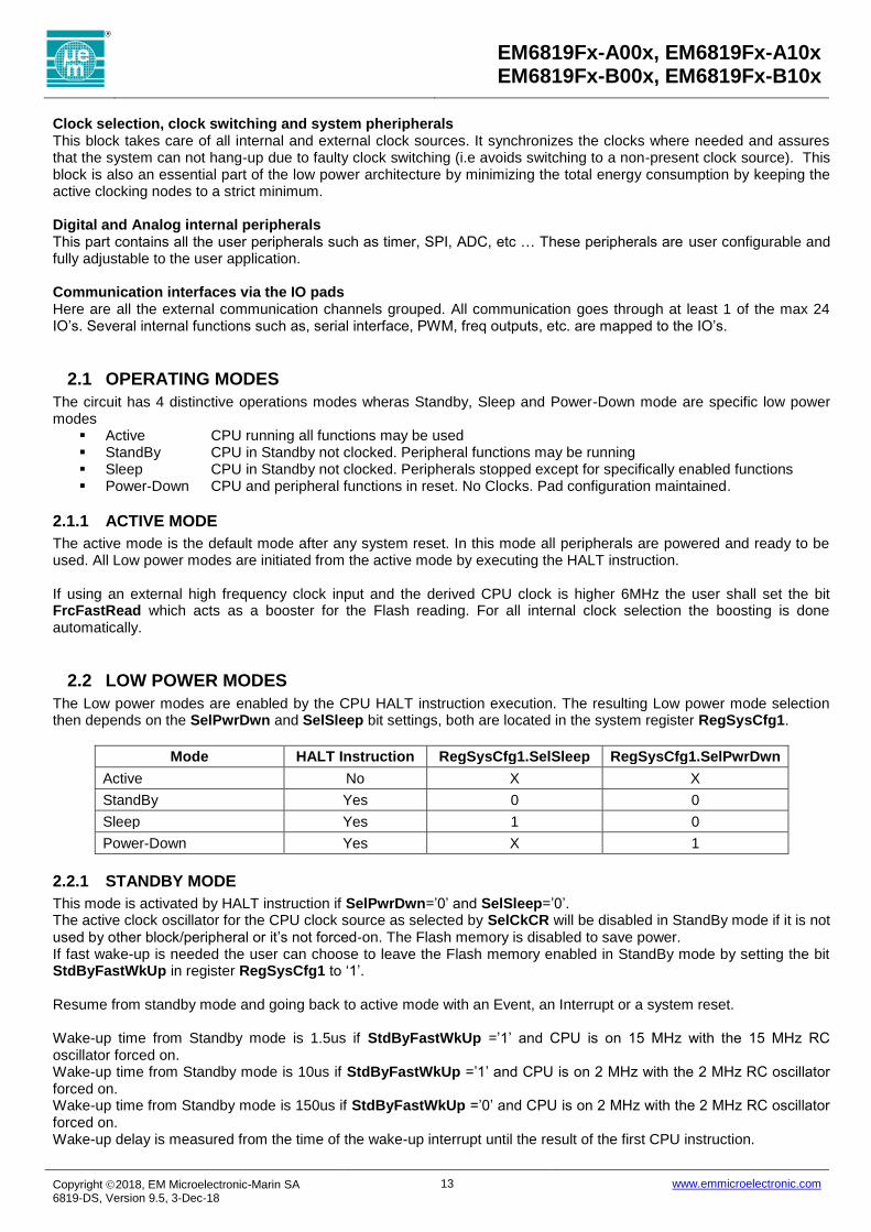
Clock selection, clock switching and system pheripherals This block takes care of all internal and external clock sources. It synchronizes the clocks where needed and assures that the system can not hang-up due to faulty clock switching (i.e avoids switching to a non-present clock source). This block is also an essential part of the low power architecture by minimizing the total energy consumption by keeping the active clocking nodes to a strict minimum. Digital and Analog internal peripherals This part contains all the user peripherals such as timer, SPI, ADC, etc … These peripherals are user configurable and fully adjustable to the user application. Communication interfaces via the IO pads Here are all the external communication channels grouped. All communication goes through at least 1 of the max 24 IO’s. Several internal functions such as, serial interface, PWM, freq outputs, etc. are mapped to the IO’s.
2.1 OPERATING MODES
The circuit has 4 distinctive operations modes wheras Standby, Sleep and Power-Down mode are specific low power modes
Active CPU running all functions may be used StandBy CPU in Standby not clocked. Peripheral functions may be running Sleep CPU in Standby not clocked. Peripherals stopped except for specifically enabled functions Power-Down CPU and peripheral functions in reset. No Clocks. Pad configuration maintained.
2.1.1 ACTIVE MODE
The active mode is the default mode after any system reset. In this mode all peripherals are powered and ready to be used. All Low power modes are initiated from the active mode by executing the HALT instruction. If using an external high frequency clock input and the derived CPU clock is higher 6MHz the user shall set the bit FrcFastRead which acts as a booster for the Flash reading. For all internal clock selection the boosting is done automatically.
2.2 LOW POWER MODES
The Low power modes are enabled by the CPU HALT instruction execution. The resulting Low power mode selection then depends on the SelPwrDwn and SelSleep bit settings, both are located in the system register RegSysCfg1.
Mode HALT Instruction RegSysCfg1.SelSleep RegSysCfg1.SelPwrDwn
Active No X X
StandBy Yes 0 0
Sleep Yes 1 0
Power-Down Yes X 1
2.2.1 STANDBY MODE
This mode is activated by HALT instruction if SelPwrDwn=’0’ and SelSleep=’0’. The active clock oscillator for the CPU clock source as selected by SelCkCR will be disabled in StandBy mode if it is not used by other block/peripheral or it’s not forced-on. The Flash memory is disabled to save power. If fast wake-up is needed the user can choose to leave the Flash memory enabled in StandBy mode by setting the bit StdByFastWkUp in register RegSysCfg1 to ‘1’. Resume from standby mode and going back to active mode with an Event, an Interrupt or a system reset. Wake-up time from Standby mode is 1.5us if StdByFastWkUp =’1’ and CPU is on 15 MHz with the 15 MHz RC oscillator forced on. Wake-up time from Standby mode is 10us if StdByFastWkUp =’1’ and CPU is on 2 MHz with the 2 MHz RC oscillator forced on. Wake-up time from Standby mode is 150us if StdByFastWkUp =’0’ and CPU is on 2 MHz with the 2 MHz RC oscillator forced on. Wake-up delay is measured from the time of the wake-up interrupt until the result of the first CPU instruction.

EM6819Fx-A00x, EM6819Fx-A10x EM6819Fx-B00x, EM6819Fx-B10x
Copyright 2018, EM Microelectronic-Marin SA 6819-DS, Version 9.5, 3-Dec-18
14 www.emmicroelectronic.com
The bit StdByFastWkUp =’1’ will increase the standby power consumption by ~1.5uA at any CPU freq settings except if the CPU is set to RC_15MHz, RC_15MHz/2 or the bit FrcFastRead is set. In these cases the extra power consumption will be ~35uA. To avoid this extra 35uA of current the user must predivide the CPU clock just before going to standby mode to values below 6MHz by
a) use RC_15MHz/4 or lower frequencies based on 2MHz, 32kHz, RC8k, b) or in case of external high freq clock input, set the CK_CPU predivider such that the resulting CPU frequeny is
below 6MHz After wake-up the original high frequency CPU clock can immediately be reinstalled with little wake-up time penalty.
Using StdByFastWkUp =’1’ together with FrcFastRead=’1’ will draw additional 35uA independent of the selected CPU clock source. It should therefore be avoided by clearing FrcFastRead before going into standby mode.
2.2.2 SLEEP MODE
This mode is activated by HALT instruction if SelPwrDwn=’0’ and SelSleep=’1’. In Sleep mode the Temperature sensor and the ADC are disabled. All oscillators are forced off except the RC 8kHz oscillator if used for sleep counter wake-up function. All register data are maintained during sleep. The Flash memory is switched off for power save. Resume from Sleep mode back to active mode with selected Interrupts and Events or by a system reset or by the sleep counter wakeup function SCWUP.
2.2.3 SLEEP WAKE-UP
Normal Wake-up from Sleep mode will take typically 250us until the 1st instruction after wake-up is executed. By setting the bit StdByFastWkUp prior to entering sleep mode the wake-up from sleep mode is greatly reduced.
In case of 2MHz RC Oscillator as CPU clock the wake-up time in fast mode is typically 18us
In case of 15MHz RC Oscillator as CPU clock the wake-up time in fast mode is typically 11us This wakeup time is measured from the wake-up event until the 3rd instruction after the wakeup event is changing a port output pin status. The bit StdByFastWkUp =’1’ will increase the sleep power consumption by ~1.5uA at any CPU freq settings except if the CPU is set to RC_15MHz, RC_15MHz/2 or the bit FrcFastRead is set. In these cases the extra power consumption will be ~35uA. To avoid this extra 35uA of current the user must predivide the CPU clock just before going to sleep mode to values below 6MHz by
c) use RC_15MHz/4 or lower frequencies based on 2MHz, 32kHz, RC8k, d) or in case of external high freq clock input, set the CK_CPU predivider such that the resulting CPU frequeny is
below 6MHz After sleep wake-up the original high frequency CPU clock can immediately be reinstalled with almost no wake-up time penalty.
Using StdByFastWkUp =’1’ together with FrcFastRead=’1’ will draw additional 35uA independent of the selected CPU clock source. It should therefore be avoided by clearing FrcFastRead before going into sleep mode. Note: DC/DC has to be switched off by the user before entering Sleep mode. Note: Interrupt sources for wake-up from the Sleep mode are defined in 12.2 Interrupt acquisition Note: Event sources for wake-up from the Sleep mode are defined in 12.8 Event acquisition

EM6819Fx-A00x, EM6819Fx-A10x EM6819Fx-B00x, EM6819Fx-B10x
Copyright 2018, EM Microelectronic-Marin SA 6819-DS, Version 9.5, 3-Dec-18
15 www.emmicroelectronic.com
2.2.4 POWER-DOWN MODE
This mode is activated by HALT instruction if SelPwrDwn=’1’. All Clocks and oscillators including the RC 8 KHz are stopped. No circuit activity anymore. All register and RAM data are lost in Power-Down mode. The device is woken-up by a level change on PortA bits or by TM=’1’; RegEnWkUpPA[n] will enable the related bit of PortA for this purpose when it is at high level. The wake-up from Power-Down acts as a reset, the CPU will start from scratch. The wake-up time from power down back to active mode is approximativly 6ms, and up to 10ms in low power mode. Note: Going into PowerDown mode without pad configuration latch shall be down in the following order:
1. Set the wake-up condition 2. Write the SelPwrDown bit 3. Execute HALT instruction
2.2.4.1 PAD CONFIGURATION LOCK IN POWER-DOWN
If the bit LckPwrCfg in register RegResFlag is set, the configurations of all Ports bits (direction, pull-up, pull-down, qblock) are locked in the pad latches. As soon as the LckPwrCfg is set back to ‘0’ the actual register configuration will be taken over. Note: To keep pad configuration in Power-Down mode, SW shall set LckPwrCfg to ‘1’ just before going into Power-Down mode and sets it to ‘0’ after wake-up from Power-Down mode. Note: Going into PowerDown mode without pad configuration latch shall be down in the following order:
1. Set the wake-up condition 2. Write the SelPwrDown bit 3. Write the LckPwrCfg bit 4. Execute HALT instruction
Note: No data are kept in the registers and in the RAM in the Power-Down mode

EM6819Fx-A00x, EM6819Fx-A10x EM6819Fx-B00x, EM6819Fx-B10x
Copyright 2018, EM Microelectronic-Marin SA 6819-DS, Version 9.5, 3-Dec-18
16 www.emmicroelectronic.com
2.2.5 OPERATION MODE REGISTERS
0x0000 RegSysCfg1 System Configuration - 1
Bits Name Type ResVal ResSrc Description
7 SelSleep RW 0 ResSys Select Sleep mode on Halt
6 SelPwrDwn RW 0 ResSys Select Power-Down mode on Halt
4 EnBrownOut RW 1 ResAna Enable Brown Out
3:2 XtalCldStart RW '00' ResSys Select Xtal Osc. ColdStart length
1 StdByFastWkUp RW 0 ResSys Stand-by mode fast Wakeup
0 VSUPLow RO 0 VSUP is Low - Tripler activated
0x0006 RegResFlg Reset Flags
Bits Name Type ResVal ResSrc Description
7 ResFlgPA ResFlg 0 PorLog Flag Reset from Port-A
6 ResFlgWD ResFlg 0 PorLog Flag Reset from WatchDog
5 ResFlgBO ResFlg 0 PorLog Flag Reset from Brown-Out
4 ResFlgGasp ResFlg 0 PorLog Flag Reset from GASP
3 ResFlgBE ResFlg 0 PorLog Flag Reset from CoolRisc Bus-Error
0 LckPwrCfg RW 0 Por Lock configurations to be kept in Power-Down mode

EM6819Fx-A00x, EM6819Fx-A10x EM6819Fx-B00x, EM6819Fx-B10x
Copyright 2018, EM Microelectronic-Marin SA 6819-DS, Version 9.5, 3-Dec-18
17 www.emmicroelectronic.com
2.3 REGISTER TYPES
The peripheral registers are of different types. The specific type of the register is marked in its table definition. Used types are: RW, RO, OS, INT, INT-SET, STS, NI, RESFLG Read-Write Register (RW) - the software is able to write high and low values - the software is able to read out the last written value - the initial and reset value is according to its specified reset value Read Only register (RO) - the software is able to read out the current status of the hardware status - the initial and reset value is according to the value of the initial hardware status or hardware status after reset One Shot register (OS) - the software wriring of the specified value is producing the given action - the software always reads a low value Interrupt status register (INT) - Software writing ‘0’ will clear a pending interrupt, clear has priority over a new arriving interrupt. - Software writing ‘1’ will set the interrupt status bit (software interrupt). This has highest priority. - If the software reads the interrupt status at ‘1’ it will clear it after the reading. - If the software reads ‘0’, no action is performed. - An incoming hardware interrupt event will set the status bit, this action has priority over clear by software read. - The reset value is ‘0’ Status register (STS) - the software can write only the allowed values into the register. These values are specified case-by-case. - the hardware may also be able to change the register value according to its function - the access priority software over hardware is specified case-by-case. - the readout value corresponds to the last change (software or hardware change) - the initial and reset value are specified case-by-case Not Implemented register (NI) - no action on write - the software is reading the specified constant value (normaly ‘0’) Reset flag register (RESFLG) - an incoming hardware event sets or clears the register according on its specification - the readout value is according to the last hardware event and specified case-by-case. - The initial and reset value is according to the value specified case-by-case defined by its last hardware event - The software is able to clear the flag by writing ‘1’ to it, writing ‘0’ has no effect - Hardware event has priority over software access.
EM6819Fx-A00x, EM6819Fx-A10x EM6819Fx-B00x, EM6819Fx-B10x
Copyright 2018, EM Microelectronic-Marin SA 6819-DS, Version 9.5, 3-Dec-18
18 www.emmicroelectronic.com
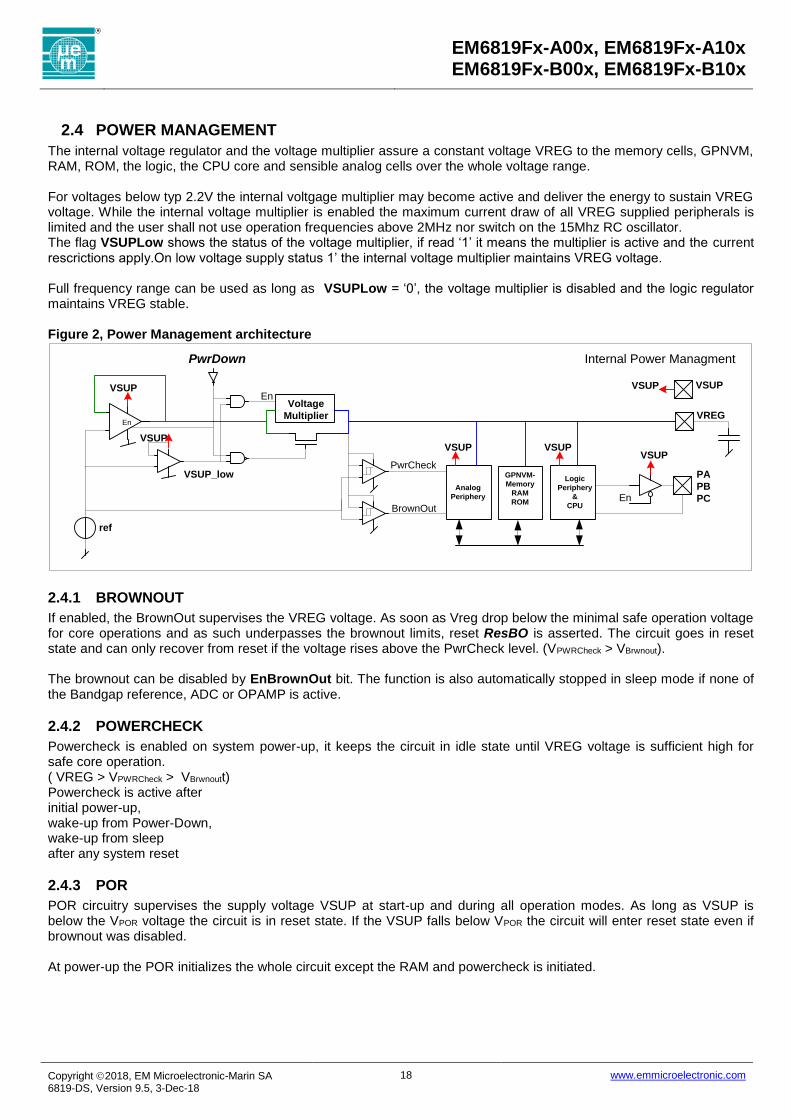
2.4 POWER MANAGEMENT
The internal voltage regulator and the voltage multiplier assure a constant voltage VREG to the memory cells, GPNVM, RAM, ROM, the logic, the CPU core and sensible analog cells over the whole voltage range. For voltages below typ 2.2V the internal voltgage multiplier may become active and deliver the energy to sustain VREG voltage. While the internal voltage multiplier is enabled the maximum current draw of all VREG supplied peripherals is limited and the user shall not use operation frequencies above 2MHz nor switch on the 15Mhz RC oscillator. The flag VSUPLow shows the status of the voltage multiplier, if read ‘1’ it means the multiplier is active and the current rescrictions apply.On low voltage supply status 1’ the internal voltage multiplier maintains VREG voltage. Full frequency range can be used as long as VSUPLow = ‘0’, the voltage multiplier is disabled and the logic regulator maintains VREG stable. Figure 2, Power Management architecture
PwrDown
VSUP_low
VSUP
VSUP
EnVoltage
Multiplier
GPNVM-
Memory
RAM
ROM
Logic
Periphery
&
CPU
Analog
Periphery
VSUPVSUP
PwrCheck
BrownOut
VSUP
En
PA
PB
PC
VREG
Internal Power Managment
ref
VSUPVSUP
En
2.4.1 BROWNOUT
If enabled, the BrownOut supervises the VREG voltage. As soon as Vreg drop below the minimal safe operation voltage for core operations and as such underpasses the brownout limits, reset ResBO is asserted. The circuit goes in reset state and can only recover from reset if the voltage rises above the PwrCheck level. (VPWRCheck > VBrwnout). The brownout can be disabled by EnBrownOut bit. The function is also automatically stopped in sleep mode if none of the Bandgap reference, ADC or OPAMP is active.
2.4.2 POWERCHECK
Powercheck is enabled on system power-up, it keeps the circuit in idle state until VREG voltage is sufficient high for safe core operation. ( VREG > VPWRCheck > VBrwnoutt) Powercheck is active after initial power-up, wake-up from Power-Down, wake-up from sleep after any system reset
2.4.3 POR
POR circuitry supervises the supply voltage VSUP at start-up and during all operation modes. As long as VSUP is below the VPOR voltage the circuit is in reset state. If the VSUP falls below VPOR the circuit will enter reset state even if brownout was disabled. At power-up the POR initializes the whole circuit except the RAM and powercheck is initiated.

EM6819Fx-A00x, EM6819Fx-A10x EM6819Fx-B00x, EM6819Fx-B10x
Copyright 2018, EM Microelectronic-Marin SA 6819-DS, Version 9.5, 3-Dec-18
19 www.emmicroelectronic.com
2.4.4 POWER MANAGMENT REGISTERS
0x0000 RegSysCfg1 System Configuration - 1
Bits Name Type ResVal ResSrc Description
7 SelSleep RW 0 ResSys Select Sleep mode on Halt
6 SelPwrDwn RW 0 ResSys Select Power-Down mode on Halt
4 EnBrownOut RW 1 ResAna Enable Brown Out
3:2 XtalCldStart RW '00' ResSys Select Xtal Osc. ColdStart length
1 StdByFastWkUp RW 0 ResSys fast Wakeup for Stand-by and Sleep mode
0 VSUPLow RO 0 VSUP is Low - Tripler activated

EM6819Fx-A00x, EM6819Fx-A10x EM6819Fx-B00x, EM6819Fx-B10x
Copyright 2018, EM Microelectronic-Marin SA 6819-DS, Version 9.5, 3-Dec-18
20 www.emmicroelectronic.com
2.5 REGISTER MAP
RegName Address Init. Bit7 Bit6 Bit5 Bit4 Bit3 Bit2 Bit1 Bit0
RegSysCfg1 0x0000 0x10 SelSleep SelPwrDwn - EnBrownOut XtalCldStart(1) XtalCldStart(0) StdByFastWkUp VSUPLow
RegEnResPA 0x0001 0x00 EnResPA(7) EnResPA(6) EnResPA(5) EnResPA(4) EnResPA(3) EnResPA(2) EnResPA(1) EnResPA(0)
RegEnWkUpPA 0x0002 0x00 EnWkUpPA(7) EnWkUpPA(6) EnWkUpPA(5) EnWkUpPA(4) EnWkUpPA(3) EnWkUpPA(2) EnWkUpPA(1) EnWkUpPA(0)
RegClockCfg1 0x0003 0x18 SelCkExt(1) SelCkExt(0) SelCkHi(1) SelCkHi(0) SelCkLo(1) SelCkLo(0) - FrcFastRead
RegClockCfg2 0x0004 0x03 FrcEnRC15M FrcEnRC2M FrcEnRC8k FrcEnExt SelCkCR(3) SelCkCR(2) SelCkCR(1) SelCkCR(0)
RegClockCfg3 0x0005 0x70 SelCkPr1(2) SelCkPr1(1) SelCkPr1(0) SelCkPr2(2) SelCkPr2(1) SelCkPr2(0) - -
RegResFlg 0x0006 0x00 ResFlgPA ResFlgWD ResFlgBO ResFlgGasp ResFlgBE - - LckPwrCfg
RegPrescCfg 0x0007 0x00 Presc1Clr Presc1Len Presc1SelIntCk5/3 Presc2Clr - - - -
RegPresc1Val 0x0008 0xFF Presc1Val(7) Presc1Val(6) Presc1Val(5) Presc1Val(4) Presc1Val(3) Presc1Val(2) Presc1Val(1) Presc1Val(0)
RegPresc2Val 0x0009 0xFF Presc2Val(7) Presc2Val(6) Presc2Val(5) Presc2Val(4) Presc2Val(3) Presc2Val(2) Presc2Val(1) Presc2Val(0)
RegPADIn 0x000A 0x00 PADIn(7) PADIn(6) PADIn(5) PADIn(4) PADIn(3) PADIn(2) PADIn(1) PADIn(0)
RegPADOut 0x000B 0x00 PADOut(7) PADOut(6) PADOut(5) PADOut(4) PADOut(3) PADOut(2) PADOut(1) PADOut(0)
RegPAInpE 0x000C 0x00 PAInpE(7) PAInpE(6) PAInpE(5) PAInpE(4) PAInpE(3) PAInpE(2) PAInpE(1) PAInpE(0)
RegPAOE 0x000D 0x00 PAOE(7) PAOE(6) PAOE(5) PAOE(4) PAOE(3) PAOE(2) PAOE(1) PAOE(0)
RegPAPU 0x000E 0x00 PAPU(7) PAPU(6) PAPU(5) PAPU(4) PAPU(3) PAPU(2) PAPU(1) PAPU(0)
RegPAPD 0x000F 0x00 PAPD(7) PAPD(6) PAPD(5) PAPD(4) PAPD(3) PAPD(2) PAPD(1) PAPD(0)
RegPAOD 0x0010 0x00 PAOD(7) PAOD(6) PAOD(5) PAOD(4) PAOD(3) PAOD(2) PAOD(1) PAOD(0)
RegPAOutCfg0 0x0011 0x00 PA3OutSel(1) PA3OutSel(0) PA2OutSel(1) PA2OutSel(0) PA1OutSel(1) PA1OutSel(0) PA0OutSel(1) PA0OutSel(0)
RegPAOutCfg1 0x0012 0x00 PA7OutSel(1) PA7OutSel(0) PA6OutSel(1) PA6OutSel(0) PA5OutSel(1) PA5OutSel(0) PA4OutSel(1) PA4OutSel(0)
RegPADebCfg1 0x0013 0x00 PA3DebSel(1) PA3DebSel(0) PA2DebSel(1) PA2DebSel(0) PA1DebSel(1) PA1DebSel(0) PA0DebSel(1) PA0DebSel(0)
RegPADebCfg2 0x0014 0x00 PA7DebSel(1) PA7DebSel(0) PA6DebSel(1) PA6DebSel(0) PA5DebSel(1) PA5DebSel(0) PA4DebSel(1) PA4DebSel(0)

EM6819Fx-A00x, EM6819Fx-A10x EM6819Fx-B00x, EM6819Fx-B10x
Copyright 2018, EM Microelectronic-Marin SA 6819-DS, Version 9.5, 3-Dec-18
21 www.emmicroelectronic.com
RegName Address Init. Bit7 Bit6 Bit5 Bit4 Bit3 Bit2 Bit1 Bit0
RegPAIntEdg 0x0015 0xFF PAIntEdg(7) PAIntEdg(6) PAIntEdg(5) PAIntEdg(4) PAIntEdg(3) PAIntEdg(2) PAIntEdg(1) PAIntEdg(0)
RegPBDIn 0x0016 0x00 PBDIn(7) PBDIn(6) PBDIn(5) PBDIn(4) PBDIn(3) PBDIn(2) PBDIn(1) PBDIn(0)
RegPBDOut 0x0017 0x00 PBDOut(7) PBDOut(6) PBDOut(5) PBDOut(4) PBDOut(3) PBDOut(2) PBDOut(1) PBDOut(0)
RegPBInpE 0x0018 0x00 PBInpE(7) PBInpE(6) PBInpE(5) PBInpE(4) PBInpE(3) PBInpE(2) PBInpE(1) PBInpE(0)
RegPBOE 0x0019 0x00 PBOE(7) PBOE(6) PBOE(5) PBOE(4) PBOE(3) PBOE(2) PBOE(1) PBOE(0)
RegPBPU 0x001A 0x00 PBPU(7) PBPU(6) PBPU(5) PBPU(4) PBPU(3) PBPU(2) PBPU(1) PBPU(0)
RegPBPD 0x001B 0x00 PBPD(7) PBPD(6) PBPD(5) PBPD(4) PBPD(3) PBPD(2) PBPD(1) PBPD(0)
RegPBOD 0x001C 0x00 PBOD(7) PBOD(6) PBOD(5) PBOD(4) PBOD(3) PBOD(2) PBOD(1) PBOD(0)
RegPBOutCfg0 0x001D 0x00 PB3OutSel(1) PB3OutSel(0) PB2OutSel(1) PB2OutSel(0) PB1OutSel(1) PB1OutSel(0) PB0OutSel(1) PB0OutSel(0)
RegPBOutCfg1 0x001E 0x00 PB7OutSel(1) PB7OutSel(0) PB6OutSel(1) PB6OutSel(0) PB5OutSel(1) PB5OutSel(0) PB4OutSel(1) PB4OutSel(0)
RegPCDIn 0x001F 0x00 PCDIn(7) PCDIn(6) PCDIn(5) PCDIn(4) PCDIn(3) PCDIn(2) PCDIn(1) PCDIn(0)
RegPCDOut 0x0020 0x00 PCDOut(7) PCDOut(6) PCDOut(5) PCDOut(4) PCDOut(3) PCDOut(2) PCDOut(1) PCDOut(0)
RegPCInpE 0x0021 0x00 PCInpE(7) PCInpE(6) PCInpE(5) PCInpE(4) PCInpE(3) PCInpE(2) PCInpE(1) PCInpE(0)
RegPCOE 0x0022 0x00 PCOE(7) PCOE(6) PCOE(5) PCOE(4) PCOE(3) PCOE(2) PCOE(1) PCOE(0)
RegPCPU 0x0023 0x00 PCPU(7) PCPU(6) PCPU(5) PCPU(4) PCPU(3) PCPU(2) PCPU(1) PCPU(0)
RegPCPD 0x0024 0x00 PCPD(7) PCPD(6) PCPD(5) PCPD(4) PCPD(3) PCPD(2) PCPD(1) PCPD(0)
RegPCOD 0x0025 0x00 PCOD(7) PCOD(6) PCOD(5) PCOD(4) PCOD(3) PCOD(2) PCOD(1) PCOD(0)
RegPCOutCfg0 0x0026 0x00 PC3OutSel(1) PC3OutSel(0) PC2OutSel(1) PC2OutSel(0) PC1OutSel(1) PC1OutSel(0) PC0OutSel(1) PC0OutSel(0)
RegPCOutCfg1 0x0027 0x00 PC7OutSel(1) PC7OutSel(0) PC6OutSel(1) PC6OutSel(0) PC5OutSel(1) PC5OutSel(0) PC4OutSel(1) PC4OutSel(0)
RegPCDebCfg1 0x0028 0x00 PC3DebSel(1) PC3DebSel(0) PC2DebSel(1) PC2DebSel(0) PC1DebSel(1) PC1DebSel(0) PC0DebSel(1) PC0DebSel(0)
RegPCDebCfg2 0x0029 0x00 PC7DebSel(1) PC7DebSel(0) PC6DebSel(1) PC6DebSel(0) PC5DebSel(1) PC5DebSel(0) PC4DebSel(1) PC4DebSel(0)
RegPCIntEdg 0x002A 0xFF PCIntEdg(7) PCIntEdg(6) PCIntEdg(5) PCIntEdg(4) PCIntEdg(3) PCIntEdg(2) PCIntEdg(1) PCIntEdg(0)
RegGaspDIn 0x002B 0x00 GaspDIn(7) GaspDIn(6) GaspDIn(5) GaspDIn(4) GaspDIn(3) GaspDIn(2) GaspDIn(1) GaspDIn(0)
RegGaspDOut 0x002C 0x00 GaspDOut(7) GaspDOut(6) GaspDOut(5) GaspDOut(4) GaspDOut(3) GaspDOut(2) GaspDOut(1) GaspDOut(0)

EM6819Fx-A00x, EM6819Fx-A10x EM6819Fx-B00x, EM6819Fx-B10x
Copyright 2018, EM Microelectronic-Marin SA 6819-DS, Version 9.5, 3-Dec-18
22 www.emmicroelectronic.com
RegName Address Init. Bit7 Bit6 Bit5 Bit4 Bit3 Bit2 Bit1 Bit0
RegGaspMode 0x002D 0x00 GaspTM GaspMode GaspSU GaspISP GaspDoC GaspTest - -
RegDoCPM1L 0x002E 0x00 DoCPM1L(7) DoCPM1L(6) DoCPM1L(5) DoCPM1L(4) DoCPM1L(3) DoCPM1L(2) DoCPM1L(1) DoCPM1L(0)
RegDoCPM1M 0x002F 0x00 - - - DoCPM1M(4) DoCPM1M(3) DoCPM1M(2) DoCPM1M(1) DoCPM1M(0)
RegDoCPM2L 0x0030 0x00 DoCPM2L(7) DoCPM2L(6) DoCPM2L(5) DoCPM2L(4) DoCPM2L(3) DoCPM2L(2) DoCPM2L(1) DoCPM2L(0)
RegDoCPM2M 0x0031 0x00 - - - DoCPM2M(4) DoCPM2M(3) DoCPM2M(2) DoCPM2M(1) DoCPM2M(0)
RegDoCPM3L 0x0032 0x00 DoCPM3L(7) DoCPM3L(6) DoCPM3L(5) DoCPM3L(4) DoCPM3L(3) DoCPM3L(2) DoCPM3L(1) DoCPM3L(0)
RegDoCPM3M 0x0033 0x00 - - - DoCPM3M(4) DoCPM3M(3) DoCPM3M(2) DoCPM3M(1) DoCPM3M(0)
RegDoCDM1L 0x0034 0x00 DoCDM1L(7) DoCDM1L(6) DoCDM1L(5) DoCDM1L(4) DoCDM1L(3) DoCDM1L(2) DoCDM1L(1) DoCDM1L(0)
RegDoCDM1M 0x0035 0x00 DoCDM1M(7) DoCDM1M(6) DoCDM1M(5) DoCDM1M(4) DoCDM1M(3) DoCDM1M(2) DoCDM1M(1) DoCDM1M(0)
RegDoCEn 0x0036 0x00 DoCEnPM1 DoCEnPM2 DoCEnPM3 DoCEnDM1(1) DoCEnDM1(0) - - -
RegDoCStat 0x0037 0x00 DoCPM1Stat DoCPM2Stat DoCPM3Stat DoCDM1Stat - - - -
RegCRC16DIn 0x0038 0x00 CRC16DIn(7) CRC16DIn(6) CRC16DIn(5) CRC16DIn(4) CRC16DIn(3) CRC16DIn(2) CRC16DIn(1) CRC16DIn(0)
RegCRC16L 0x0039 0x00 CRC16L(7) CRC16L(6) CRC16L(5) CRC16L(4) CRC16L(3) CRC16L(2) CRC16L(1) CRC16L(0)
RegCRC16M 0x003A 0x00 CRC16M(7) CRC16M(6) CRC16M(5) CRC16M(4) CRC16M(3) CRC16M(2) CRC16M(1) CRC16M(0)
RegTimersCfg 0x003B 0x00 Tim12Chain Tim34Chain Tim1AR Tim2AR Tim3AR Tim4AR Tim1SWCpt Tim3SWCpt
RegTimersStart 0x003C 0x00 Tim1SWStart Tim1Pulse Tim2SWStart Tim2Pulse Tim3SWStart Tim3Pulse Tim4SWStart Tim4Pulse
RegTim1Cfg 0x003D 0x00 Tim1EnPWM Tim1IntSel Tim1SelStart(2) Tim1SelStart(1) Tim1SelStart(0) Tim1SelClk(2) Tim1SelClk(1) Tim1SelClk(0)
RegTim1CptCmpCfg 0x003E 0x00 Tim1CptEdg(1) Tim1CptEdg(0) Tim1CptEvtSrc(1) Tim1CptEvtSrc(0) Tim1CmpFullAct(1) Tim1CmpFullAct(0) Tim1CmpValAct(1) Tim1CmpValAct(0)
RegTim1Status 0x003F 0x00 Tim1Status(7) Tim1Status(6) Tim1Status(5) Tim1Status(4) Tim1Status(3) Tim1Status(2) Tim1Status(1) Tim1Status(0)
RegTim1Full 0x0040 0xFF Tim1Full(7) Tim1Full(6) Tim1Full(5) Tim1Full(4) Tim1Full(3) Tim1Full(2) Tim1Full(1) Tim1Full(0)
RegTim1CmpVal 0x0041 0x00 Tim1CmpVal(7) Tim1CmpVal(6) Tim1CmpVal(5) Tim1CmpVal(4) Tim1CmpVal(3) Tim1CmpVal(2) Tim1CmpVal(1) Tim1CmpVal(0)
RegTim1CptVal 0x0042 0x00 Tim1CptVal(7) Tim1CptVal(6) Tim1CptVal(5) Tim1CptVal(4) Tim1CptVal(3) Tim1CptVal(2) Tim1CptVal(1) Tim1CptVal(0)
RegTim2Cfg 0x0043 0x00 Tim2EnPWM Tim2IntSel Tim2SelStart(2) Tim2SelStart(1) Tim2SelStart(0) Tim2SelClk(2) Tim2SelClk(1) Tim2SelClk(0)
RegTim2CptCmpCfg 0x0044 0x00 Tim2CptEdg(1) Tim2CptEdg(0) Tim2CptEvtSrc(1) Tim2CptEvtSrc(0) Tim2CmpFullAct(1) Tim2CmpFullAct(0) Tim2CmpValAct(1) Tim2CmpValAct(0)

EM6819Fx-A00x, EM6819Fx-A10x EM6819Fx-B00x, EM6819Fx-B10x
Copyright 2018, EM Microelectronic-Marin SA 6819-DS, Version 9.5, 3-Dec-18
23 www.emmicroelectronic.com
RegName Address Init. Bit7 Bit6 Bit5 Bit4 Bit3 Bit2 Bit1 Bit0
RegTim2Status 0x0045 0x00 Tim2Status(7) Tim2Status(6) Tim2Status(5) Tim2Status(4) Tim2Status(3) Tim2Status(2) Tim2Status(1) Tim2Status(0)
RegTim2Full 0x0046 0xFF Tim2Full(7) Tim2Full(6) Tim2Full(5) Tim2Full(4) Tim2Full(3) Tim2Full(2) Tim2Full(1) Tim2Full(0)
RegTim2CmpVal 0x0047 0x00 Tim2CmpVal(7) Tim2CmpVal(6) Tim2CmpVal(5) Tim2CmpVal(4) Tim2CmpVal(3) Tim2CmpVal(2) Tim2CmpVal(1) Tim2CmpVal(0)
RegTim2CptVal 0x0048 0x00 Tim2CptVal(7) Tim2CptVal(6) Tim2CptVal(5) Tim2CptVal(4) Tim2CptVal(3) Tim2CptVal(2) Tim2CptVal(1) Tim2CptVal(0)
RegTim3Cfg 0x0049 0x00 Tim3EnPWM Tim3IntSel Tim3SelStart(2) Tim3SelStart(1) Tim3SelStart(0) Tim3SelClk(2) Tim3SelClk(1) Tim3SelClk(0)
RegTim3CptCmpCfg 0x004A 0x00 Tim3CptEdg(1) Tim3CptEdg(0) Tim3CptEvtSrc(1) Tim3CptEvtSrc(0) Tim3CmpFullAct(1) Tim3CmpFullAct(0) Tim3CmpValAct(1) Tim3CmpValAct(0)
RegTim3Status 0x004B 0x00 Tim3Status(7) Tim3Status(6) Tim3Status(5) Tim3Status(4) Tim3Status(3) Tim3Status(2) Tim3Status(1) Tim3Status(0)
RegTim3Full 0x004C 0xFF Tim3Full(7) Tim3Full(6) Tim3Full(5) Tim3Full(4) Tim3Full(3) Tim3Full(2) Tim3Full(1) Tim3Full(0)
RegTim3CmpVal 0x004D 0x00 Tim3CmpVal(7) Tim3CmpVal(6) Tim3CmpVal(5) Tim3CmpVal(4) Tim3CmpVal(3) Tim3CmpVal(2) Tim3CmpVal(1) Tim3CmpVal(0)
RegTim3CptVal 0x004E 0x00 Tim3CptVal(7) Tim3CptVal(6) Tim3CptVal(5) Tim3CptVal(4) Tim3CptVal(3) Tim3CptVal(2) Tim3CptVal(1) Tim3CptVal(0)
RegTim4Cfg 0x004F 0x00 Tim4EnPWM Tim4IntSel Tim4SelStart(2) Tim4SelStart(1) Tim4SelStart(0) Tim4SelClk(2) Tim4SelClk(1) Tim4SelClk(0)
RegTim4CptCmpCfg 0x0050 0x00 Tim4CptEdg(1) Tim4CptEdg(0) Tim4CptEvtSrc(1) Tim4CptEvtSrc(0) Tim4CmpFullAct(1) Tim4CmpFullAct(0) Tim4CmpValAct(1) Tim4CmpValAct(0)
RegTim4Status 0x0051 0x00 Tim4Status(7) Tim4Status(6) Tim4Status(5) Tim4Status(4) Tim4Status(3) Tim4Status(2) Tim4Status(1) Tim4Status(0)
RegTim4Full 0x0052 0xFF Tim4Full(7) Tim4Full(6) Tim4Full(5) Tim4Full(4) Tim4Full(3) Tim4Full(2) Tim4Full(1) Tim4Full(0)
RegTim4CmpVal 0x0053 0x00 Tim4CmpVal(7) Tim4CmpVal(6) Tim4CmpVal(5) Tim4CmpVal(4) Tim4CmpVal(3) Tim4CmpVal(2) Tim4CmpVal(1) Tim4CmpVal(0)
RegTim4CptVal 0x0054 0x00 Tim4CptVal(7) Tim4CptVal(6) Tim4CptVal(5) Tim4CptVal(4) Tim4CptVal(3) Tim4CptVal(2) Tim4CptVal(1) Tim4CptVal(0)
RegADCCfg1 0x0055 0x00 EnADC RunContMeas RunSinglMeas EnTempSens ADCSmplRate(2) ADCSmplRate(1) ADCSmplRate(0) ADC8bit
RegADCCfg2 0x0056 0x00 ADCSelRef(1) ADCSelRef(0) ADCSelRange(1) ADCSelRange(0) ADCLowNoise - - -
RegADCOut0 0x0057 0x00 ADCOut0(7) ADCOut0(6) ADCOut0(5) ADCOut0(4) ADCOut0(3) ADCOut0(2) ADCOut0(1) ADCOut0(0)
RegADCOut1 0x0058 0x00 ADCBusy ADCSelSrc(2) ADCSelSrc(1) ADCSelSrc(0) StsTempSens ADCOutLSB ADCOut1(1) ADCOut1(0)
RegADCOffsetL 0x0059 0x00 ADCOffsetL(7) ADCOffsetL(6) ADCOffsetL(5) ADCOffsetL(4) ADCOffsetL(3) ADCOffsetL(2) ADCOffsetL(1) ADCOffsetL(0)
RegADCOffsetM 0x005A 0x04 - - - - - ADCOffsetM(2) ADCOffsetM(1) ADCOffsetM(0)
RegOpAmpCfg1 0x005B 0x00 EnOpAmp EnComp OpAmpSup CompRes SelCompInt(1) SelCompInt(0) - -
RegOpAmpCfg2 0x005C 0x00 OpAmpSelInpPos(1) OpAmpSelInpPos(0) OpAmpSelInpNeg(1) OpAmpSelInpNeg(0) OpAmpSelOut - - -

EM6819Fx-A00x, EM6819Fx-A10x EM6819Fx-B00x, EM6819Fx-B10x
Copyright 2018, EM Microelectronic-Marin SA 6819-DS, Version 9.5, 3-Dec-18
24 www.emmicroelectronic.com
RegName Address Init. Bit7 Bit6 Bit5 Bit4 Bit3 Bit2 Bit1 Bit0
RegDC-DCCfg 0x005D 0x00 EnDC-DC DC-DCLevel(1) DC-DCLevel(0) DC-DCIdle DC-DCStartSts - - -
RegVLDCfg1 0x005E 0x00 EnVLD VLDRes VLDSelSrc(2) VLDSelSrc(1) VLDSelSrc(0) - - -
RegVLDCfg2 0x005F 0x00 - - - VLDSelLvl(4) VLDSelLvl(3) VLDSelLvl(2) VLDSelLvl(1) VLDSelLvl(0)
RegBgrCfg 0x0060 0x00 BgrEnOut NVMEnWrite - - - - - -
RegInt0Sts 0x0061 0x00 Int0StsPort(0) Int0StsTim1 Int0StsPr1Ck0 Int0StsADC Int0StsDoCDM Int0StsDoCPM Int0StsGasp Int0StsPMMiss
RegInt1Sts 0x0062 0x00 Int1StsPort(2) Int1StsPort(1) Int1StsTim2 Int1StsTim3 Int1StsOpAmp Int1StsPr1Ck5/3 Int1StsSPIStop Int1StsSPIStart
RegInt2Sts 0x0063 0x00 Int2StsVLD Int2StsSlpCnt Int2StsPort(7) Int2StsPort(6) Int2StsPort(5) Int2StsPort(4) Int2StsPort(3) Int2StsTim4
RegInt0Msk 0x0064 0x00 Int0MskPort(0) Int0MskTim1 Int0MskPr1Ck0 Int0MskADC Int0MskDoCDM Int0MskDoCPM Int0MskGasp Int0MskPMMiss
RegInt1Msk 0x0065 0x00 Int1MskPort(2) Int1MskPort(1) Int1MskTim2 Int1MskTim3 Int1MskOpAmp Int1MskPr1Ck5/3 Int1MskSPIStop Int1MskSPIStart
RegInt2Msk 0x0066 0x00 Int2MskVLD Int2MskSlpCnt Int2MskPort(7) Int2MskPort(6) Int2MskPort(5) Int2MskPort(4) Int2MskPort(3) Int2MskTim4
RegInt0PostMsk 0x0067 0x00 Int0PostMskPort(0) Int0PostMskTim1 Int0PostMskPr1Ck0 Int0PostMskADC Int0PostMskDoCDM Int0PostMskDoCPM Int0PostMskGasp Int0PostMskPMMiss
RegInt1PostMsk 0x0068 0x00 Int1PostMskPort(2) Int1PostMskPort(1) Int1PostMskTim2 Int1PostMskTim3 Int1PostMskOpAmp Int1PostMskPr1Ck5/3 Int1PostMskSPIStop Int1PostMskSPIStart
RegInt2PostMsk 0x0069 0x00 Int2PostMskVLD Int2PostMskSlpCnt Int2PostMskPort(7) Int2PostMskPort(6) Int2PostMskPort(5) Int2PostMskPort(4) Int2PostMskPort(3) Int2PostMskTim4
RegIntPortSrc 0x006A 0x00 IntPortSrc(7) IntPortSrc(6) IntPortSrc(5) IntPortSrc(4) IntPortSrc(3) IntPortSrc(2) IntPortSrc(1) IntPortSrc(0)
RegEvtSts 0x006B 0x00 - - - - Evt1StsSlpCnt Evt1StsSPI Evt1StsADC Evt0StsGasp
RegEvtCfg 0x006C 0x00 Evt1PostMskSC Evt1MskSC Evt1PostMskSPI Evt1MskSPI Evt1PostMskADC Evt1MskADC Evt0PostMskGasp Evt0MskGasp
RegWDCfg 0x006D 0x00 WDDis - - - - - - WDClear
RegWDKey 0x006E 0x00 WDKey(7) WDKey(6) WDKey(5) WDKey(4) WDKey(3) WDKey(2) WDKey(1) WDKey(0)
RegWDLdValL 0x006F 0x00 WDLdValL(7) WDLdValL(6) WDLdValL(5) WDLdValL(4) WDLdValL(3) WDLdValL(2) WDLdValL(1) WDLdValL(0)
RegWDLdValM 0x0070 0x80 WDLdValM(7) WDLdValM(6) WDLdValM(5) WDLdValM(4) WDLdValM(3) WDLdValM(2) WDLdValM(1) WDLdValM(0)
RegWDStatL 0x0071 0x00 WDStatL(7) WDStatL(6) WDStatL(5) WDStatL(4) WDStatL(3) WDStatL(2) WDStatL(1) WDStatL(0)
RegWDStatM 0x0072 0x80 WDStatM(7) WDStatM(6) WDStatM(5) WDStatM(4) WDStatM(3) WDStatM(2) WDStatM(1) WDStatM(0)
RegSCCfg 0x0073 0x00 SCDis SCStart - - - - - -
RegSCLdVal0 0x0074 0x00 SCLdVal0(7) SCLdVal0(6) SCLdVal0(5) SCLdVal0(4) SCLdVal0(3) SCLdVal0(2) SCLdVal0(1) SCLdVal0(0)

EM6819Fx-A00x, EM6819Fx-A10x EM6819Fx-B00x, EM6819Fx-B10x
Copyright 2018, EM Microelectronic-Marin SA 6819-DS, Version 9.5, 3-Dec-18
25 www.emmicroelectronic.com
RegName Address Init. Bit7 Bit6 Bit5 Bit4 Bit3 Bit2 Bit1 Bit0
RegSCLdVal1 0x0075 0x80 SCLdVal1(7) SCLdVal1(6) SCLdVal1(5) SCLdVal1(4) SCLdVal1(3) SCLdVal1(2) SCLdVal1(1) SCLdVal1(0)
RegSCLdVal2 0x0076 0x00 SCLdVal2(7) SCLdVal2(6) SCLdVal2(5) SCLdVal2(4) SCLdVal2(3) SCLdVal2(2) SCLdVal2(1) SCLdVal2(0)
RegSCStat0 0x0077 0x00 SCStat0(7) SCStat0(6) SCStat0(5) SCStat0(4) SCStat0(3) SCStat0(2) SCStat0(1) SCStat0(0)
RegSCStat1 0x0078 0x80 SCStat1(7) SCStat1(6) SCStat1(5) SCStat1(4) SCStat1(3) SCStat1(2) SCStat1(1) SCStat1(0)
RegSCStat2 0x0079 0x00 SCStat2(7) SCStat2(6) SCStat2(5) SCStat2(4) SCStat2(3) SCStat2(2) SCStat2(1) SCStat2(0)
RegSPICfg1 0x007A 0x03 SPIEn SPIMode(2) SPIMode(1) SPIMode(0) SPINegEdg SPIRTO SPIMSB1st SPIAutoStart
RegSPICfg2 0x007B 0x00 SPISelSClk(1) SPISelSClk(0) SPISelSIn(1) SPISelSIn(0) - - - -
RegSPIStart 0x007C 0x00 SPIStart - - - - - - -
RegSPIDIn 0x007D 0x00 SPIDIn(7) SPIDIn(6) SPIDIn(5) SPIDIn(4) SPIDIn(3) SPIDIn(2) SPIDIn(1) SPIDIn(0)
RegSPIDOut 0x007E 0x00 SPIDOut(7) SPIDOut(6) SPIDOut(5) SPIDOut(4) SPIDOut(3) SPIDOut(2) SPIDOut(1) SPIDOut(0)
RegCacheB00 0x0280 0x00 CacheB00(7) CacheB00(6) CacheB00(5) CacheB00(4) CacheB00(3) CacheB00(2) CacheB00(1) CacheB00(0)
RegCacheB01 0x0281 0x00 CacheB01(7) CacheB01(6) CacheB01(5) CacheB01(4) CacheB01(3) CacheB01(2) CacheB01(1) CacheB01(0)
RegCacheB02 0x0282 0x00 CacheB02(7) CacheB02(6) CacheB02(5) CacheB02(4) CacheB02(3) CacheB02(2) CacheB02(1) CacheB02(0)
RegCacheB03 0x0283 0x00 CacheB03(7) CacheB03(6) CacheB03(5) CacheB03(4) CacheB03(3) CacheB03(2) CacheB03(1) CacheB03(0)
RegCacheB04 0x0284 0x00 CacheB04(7) CacheB04(6) CacheB04(5) CacheB04(4) CacheB04(3) CacheB04(2) CacheB04(1) CacheB04(0)
RegCacheB05 0x0285 0x00 CacheB05(7) CacheB05(6) CacheB05(5) CacheB05(4) CacheB05(3) CacheB05(2) CacheB05(1) CacheB05(0)
RegCacheB06 0x0286 0x00 CacheB06(7) CacheB06(6) CacheB06(5) CacheB06(4) CacheB06(3) CacheB06(2) CacheB06(1) CacheB06(0)
RegCacheB07 0x0287 0x00 CacheB07(7) CacheB07(6) CacheB07(5) CacheB07(4) CacheB07(3) CacheB07(2) CacheB07(1) CacheB07(0)
RegCacheB08 0x0288 0x00 CacheB08(7) CacheB08(6) CacheB08(5) CacheB08(4) CacheB08(3) CacheB08(2) CacheB08(1) CacheB08(0)
RegCacheB09 0x0289 0x00 CacheB09(7) CacheB09(6) CacheB09(5) CacheB09(4) CacheB09(3) CacheB09(2) CacheB09(1) CacheB09(0)
RegCacheB10 0x028A 0x00 CacheB10(7) CacheB10(6) CacheB10(5) CacheB10(4) CacheB10(3) CacheB10(2) CacheB10(1) CacheB10(0)
RegCacheB11 0x028B 0x00 CacheB11(7) CacheB11(6) CacheB11(5) CacheB11(4) CacheB11(3) CacheB11(2) CacheB11(1) CacheB11(0)
RegCacheB12 0x028C 0x00 CacheB12(7) CacheB12(6) CacheB12(5) CacheB12(4) CacheB12(3) CacheB12(2) CacheB12(1) CacheB12(0)
RegCacheB13 0x028D 0x00 CacheB13(7) CacheB13(6) CacheB13(5) CacheB13(4) CacheB13(3) CacheB13(2) CacheB13(1) CacheB13(0)

EM6819Fx-A00x, EM6819Fx-A10x EM6819Fx-B00x, EM6819Fx-B10x
Copyright 2018, EM Microelectronic-Marin SA 6819-DS, Version 9.5, 3-Dec-18
26 www.emmicroelectronic.com
RegName Address Init. Bit7 Bit6 Bit5 Bit4 Bit3 Bit2 Bit1 Bit0
RegCacheB14 0x028E 0x00 CacheB14(7) CacheB14(6) CacheB14(5) CacheB14(4) CacheB14(3) CacheB14(2) CacheB14(1) CacheB14(0)
RegCacheB15 0x028F 0x00 CacheB15(7) CacheB15(6) CacheB15(5) CacheB15(4) CacheB15(3) CacheB15(2) CacheB15(1) CacheB15(0)
RegCacheB16 0x0290 0x00 CacheB16(7) CacheB16(6) CacheB16(5) CacheB16(4) CacheB16(3) CacheB16(2) CacheB16(1) CacheB16(0)
RegCacheB17 0x0291 0x00 CacheB17(7) CacheB17(6) CacheB17(5) CacheB17(4) CacheB17(3) CacheB17(2) CacheB17(1) CacheB17(0)
RegCacheB18 0x0292 0x00 CacheB18(7) CacheB18(6) CacheB18(5) CacheB18(4) CacheB18(3) CacheB18(2) CacheB18(1) CacheB18(0)
RegCacheB19 0x0293 0x00 CacheB19(7) CacheB19(6) CacheB19(5) CacheB19(4) CacheB19(3) CacheB19(2) CacheB19(1) CacheB19(0)
RegCacheB20 0x0294 0x00 CacheB20(7) CacheB20(6) CacheB20(5) CacheB20(4) CacheB20(3) CacheB20(2) CacheB20(1) CacheB20(0)
RegCacheB21 0x0295 0x00 CacheB21(7) CacheB21(6) CacheB21(5) CacheB21(4) CacheB21(3) CacheB21(2) CacheB21(1) CacheB21(0)
RegCacheB22 0x0296 0x00 CacheB22(7) CacheB22(6) CacheB22(5) CacheB22(4) CacheB22(3) CacheB22(2) CacheB22(1) CacheB22(0)
RegCacheB23 0x0297 0x00 CacheB23(7) CacheB23(6) CacheB23(5) CacheB23(4) CacheB23(3) CacheB23(2) CacheB23(1) CacheB23(0)
RegCacheB24 0x0298 0x00 CacheB24(7) CacheB24(6) CacheB24(5) CacheB24(4) CacheB24(3) CacheB24(2) CacheB24(1) CacheB24(0)
RegCacheB25 0x0299 0x00 CacheB25(7) CacheB25(6) CacheB25(5) CacheB25(4) CacheB25(3) CacheB25(2) CacheB25(1) CacheB25(0)
RegCacheB26 0x029A 0x00 CacheB26(7) CacheB26(6) CacheB26(5) CacheB26(4) CacheB26(3) CacheB26(2) CacheB26(1) CacheB26(0)
RegCacheB27 0x029B 0x00 CacheB27(7) CacheB27(6) CacheB27(5) CacheB27(4) CacheB27(3) CacheB27(2) CacheB27(1) CacheB27(0)
RegCacheB28 0x029C 0x00 CacheB28(7) CacheB28(6) CacheB28(5) CacheB28(4) CacheB28(3) CacheB28(2) CacheB28(1) CacheB28(0)
RegCacheB29 0x029D 0x00 CacheB29(7) CacheB29(6) CacheB29(5) CacheB29(4) CacheB29(3) CacheB29(2) CacheB29(1) CacheB29(0)
RegCacheB30 0x029E 0x00 CacheB30(7) CacheB30(6) CacheB30(5) CacheB30(4) CacheB30(3) CacheB30(2) CacheB30(1) CacheB30(0)
RegCacheB31 0x029F 0x00 CacheB31(7) CacheB31(6) CacheB31(5) CacheB31(4) CacheB31(3) CacheB31(2) CacheB31(1) CacheB31(0)
RegCacheCfg1 0x02A0 0x00 - - CacheRow(5) CacheRow(4) CacheRow(3) CacheRow(2) CacheRow(1) CacheRow(0)
RegCacheCfg2 0x02A1 0x80 NVMFastProg - - - - CacheSector(2) CacheSector(1) CacheSector(0)
RegTrimOsc15M 0x02A2 0x80 TrimOsc15M(7) TrimOsc15M(6) TrimOsc15M(5) TrimOsc15M(4) TrimOsc15M(3) TrimOsc15M(2) TrimOsc15M(1) TrimOsc15M(0)
RegTrimOsc2M 0x02A3 0x80 TrimOsc2M(7) TrimOsc2M(6) TrimOsc2M(5) TrimOsc2M(4) TrimOsc2M(3) TrimOsc2M(2) TrimOsc2M(1) TrimOsc2M(0)
RegTrimVLD 0x02A4 0x08 - - - - TrimVLD(3) TrimVLD(2) TrimVLD(1) TrimVLD(0)
RegStsCStart 0x02A5 0x39 - - StsCSReson StsCSXtal StsCSPad StsCSRC8k StsCSRC2M StsCSRC15M
RegName Address Init. Bit7 Bit6 Bit5 Bit4 Bit3 Bit2 Bit1 Bit0
RegStsEnOsc 0x02A6 0x06 - - - StsEnReson StsEnXtal StsEnRC8k StsEnRC2M StsEnRC15M
RegCkSw1 0x02A7 0x12 CkSwSelX CkSwStsX CkSwSelHi(2) CkSwSelHi(1) CkSwSelHi(0) CkSwStsHi(2) CkSwStsHi(1) CkSwStsHi(0)
RegCkSw2 0x02A8 0x24 - - CkSwSelLo(2) CkSwSelLo(1) CkSwSelLo(0) CkSwStsLo(2) CkSwStsLo(1) CkSwStsLo(0)

EM6819Fx-A00x, EM6819Fx-A10x EM6819Fx-B00x, EM6819Fx-B10x
Copyright 2018, EM Microelectronic-Marin SA 6819-DS, Version 9.5, 3-Dec-18
27 www.emmicroelectronic.com
2.6 PORT TERMINAL CONNECTION REFERENCE TABLE
chip Name Base IRQ ADC
Reset &
WkUp VREF VLD OPAMP SPI GASP CLOCK
Timer
clock
Timer
start
PWM
FrqOut
high
drive
Nbr
1 VSS2 SUP VSS protection pad to reduce noisedouble bond
2 VSS SUP main VSS
3 PB2 IO SCLK sig HD
4 PB3 IO sig HD
5 PB4 IO SOUT sig HD
6 PB5 IO sig HD
7 PB6 IO GASP-SCK sig HD
8 PB7 IO GASP-SIO sig HD
9 PA0 IO PAIRQ0 ADC0 Rst_Wkup0 t1ck0_in start1_in sig
10 PC0 IO PCIRQ0 ADC1 sig
11 PA1 IO PAIRQ1 ADC2 Rst_Wkup1 VLD OPA_Out t2ck0_in start2_in sig
12 PC1 IO PCIRQ1 ADC3 VLD OPA_Out t2ck1_in start3_in sig
13 PA2 IO PAIRQ2 ADC4 Rst_Wkup2 Vref_ADC VLD OPA_INMSIN
SOUTt3ck0_in start4_in sig
14 PC2 IO PAIRQ2 ADC5 OPA_INM SOUT sig
15 PA3 IO PAIRQ3 ADC6 Rst_Wkup3 OPA_INP t4ck0_in start5_in sig HD
16 PC3 IO PCIRQ3 ADC7 OPA_INP t4ck1_in start6_in sig HD
17 VREG SUP use external Capacitor
18 PA4 IO PAIRQ4 Rst_Wkup4 SIN XIN sig
19 PC4 IO PCIRQ4XOUT
ExtCksig
20 TM IN GASP-Sel21 PA5 IO PAIRQ5 Rst_Wkup5 sig HD
22 PC5 IO PCIRQ5 VLD sig HD
23 PC6 IO PCIRQ6 VLD SCLK t1ck1_in start7_in sig HD
24 PA6 IO PAIRQ6 Rst_Wkup6 Vref_out VLD SCLK sig HD
25 PA7 IO PAIRQ7 Rst_Wkup7 VLD SOUT sig HD
26 PC7 IO PCIRQ7 t3ck1_in sig
27 PB0 IO SIN sig HD
28 PB1 IO sig HD
29 VSUP SUP
30 VSUP2 SUP VSUP protection pad to reduce noise
31 DCDC SUP DCDC Coil connection in case of DCDC Version, open (not bonded, if no DCDC)
32 VSSDCDC SUP VSS for DCDC, not bonded for non DCDC versions

EM6819Fx-A00x, EM6819Fx-A10x EM6819Fx-B00x, EM6819Fx-B10x
Copyright 2018, EM Microelectronic-Marin SA 6819-DS, Version 9.5, 3-Dec-18
28 www.emmicroelectronic.com
2.7 TSSOP PACKAGE PINOUT CIRCUIT WITHOUT DC-DC AND S08
PB5
PB6
PB7
PA0
PC0
PA1
PC1
PA2
PC2
PA3
PC3
Vreg
PA4
PC4 TM
PA5
PC5
PA6
PC6
PA7
PC7
PB0
PB1
VSUP
VSS
PB2
PB3
PB41
2
3
4
5
6
7
8
9
10
11
12
13
14 15
16
17
18
19
20
21
22
23
24
25
26
27
28IO
IO/GASP-CK
IO/GASP-DIO
IO/Tim/Rst0/
ADC0
IO/
ADC1
IO/Tim/Rst1/
VLD/ADC2/OPA-Out
IO/Tim/
VLD/ADC3/OPA-Out
IO/SIN/SOUT/Tim/Rst2/
ADC4/VLD/OPA-INM
IO/SOUT/
ADC5/OPA-INM
IO/Tim/Rst3/
ADC6/OPA-INP
IO/Tim/
ADC7/OPA-INP
GASP-Sel
IO/SIN/Rst4/
Xin
IO/ExtCK/
Xout
IO/Rst5/
IO/
VLD
IO/SCLK/Rst6/
Vref/VLD
IO/SCLK/Tim/
VLD
IO/SOUT/Rst7/
VLD
IO/Tim
IO/SIN
IO
IO/SCLK
IO
IO/SOUT
28-LeadTSSOP
4.40mm body
EM6819FX-BXXX
EM
68
19
PB5
PB6
PB7
PA0
PA1
PC1
PA2
PC2
PA3
Vreg
PA4
PC4 TM
PA5
PC5
PA6
PC6
PA7
PC7
VSUP
VSS
PB2
PB3
PB41
2
3
4
5
6
7
8
9
10
11
12 13
14
15
16
17
18
19
20
21
22
23
24IO
IO/GASP-CK
IO/GASP-DIO
IO/Tim/Rst0/
ADC0
IO/Tim/Rst1/
VLD/ADC2/OPA-Out
IO/Tim/
VLD/ADC3/OPA-Out
IO/SIN/SOUT/Tim/Rst2/
ADC4/VLD/OPA-INM
IO/SOUT/
ADC5/OPA-INM
IO/Tim/Rst3/
ADC6/OPA-INP
GASP-Sel
IO/SIN/Rst4/
Xin
IO/ExtCK/
Xout
IO/Rst5/
IO/
VLD
IO/SCLK/Rst6/
Vref/VLD
IO/SCLK/Tim/
VLD
IO/SOUT/Rst7/
VLD
IO/Tim
IO/SCLK
IO
IO/SOUT
24-Lead TSSOP
4.40mm body
EM6819FX-BXXX
EM
68
19
PB5
PB6
PB7
PA1
PA2
PC2
PA3
Vreg
PA4 PC4
TM
PC5
PA6
PC6
PA7
VSUP
VSS
PB2
PB3
2
3
4
5
6
7
8
9
10 11
12
13
14
15
16
17
18
19
20
IO
IO/GASP-CK
IO/GASP-DIO
IO/Tim/Rst1/
VLD/ADC2/OPA-Out
IO/SIN/SOUT/Tim/Rst2/
ADC4/VLD/OPA-INM
IO/SOUT/
ADC5/OPA-INM
IO/Tim/Rst3/
ADC6/OPA-INP
GASP-Sel
IO/SIN/Rst4/
Xin
IO/ExtCK/
Xout
IO/
VLD
IO/SCLK/Rst6/
Vref/VLD
IO/SCLK/Tim/
VLD
IO/SOUT/Rst7/
VLD
IO/SCLK
IO
20-Lead TSSOP
4.40mm body
EM6819FX-BXXX
PB41IO/SOUT
EM
68
19
PB6
PB7
PA1
PA2
PA3
Vreg
PA4 PC4
TM
PA6
PC6
PA7
VSUP
VSS
PB2
2
3
4
5
6
7
8 9
10
11
12
13
14
15
16
IO/GASP-CK
IO/GASP-DIO
IO/Tim/Rst1/
VLD/ADC2/OPA-Out
IO/SIN/SOUT/Tim/Rst2/
ADC4/VLD/OPA-INM
IO/Tim/Rst3/
ADC6/OPA-INP
GASP-Sel
IO/SIN/Rst4/
Xin
IO/ExtCK/
Xout
IO/SCLK/Rst6/
Vref/VLD
IO/SCLK/Tim/
VLD
IO/SOUT/Rst7/
VLD
IO/SCLK
16-Lead TSSOP
4.40mm body
EM6819FX-BXX0
EM6819FX-BXX4
PB41IO/SOUT
EM
68
19
PB6
PB7
PA2
Vreg TM
PA6
VSUP
VSS1
2
3
4 5
6
7
8IO/GASP-CK
IO/GASP-DIO
IO/SIN/SOUT/Tim/Rst2/
ADC4/VLD/OPA-INM
GASP-Sel
IO/SCLK/Rst6/
Vref/VLD
8-Lead SOIC-150
EM6819FX-BXXX
EM
68
19
PB6
PB7
PA1
PA2
PA3
Vreg PA4
PC4
TM
PA6
PC6
VSUP
VSS
PB2
2
3
4
5
6
7
8 9
10
11
12
13
14
15
16
IO/GASP-CK
IO/GASP-DIO
IO/Tim/Rst1/
VLD/ADC2/OPA-Out
IO/SIN/SOUT/Tim/Rst2/
ADC4/VLD/OPA-INM
IO/Tim/Rst3/
ADC6/OPA-INP
GASP-Sel
IO/SIN/Rst4/
IO
IO/SCLK/Rst6/
Vref/VLD
IO/SCLK/Tim/
VLD
IO/SCLK
16-Lead TSSOP
4.40mm body
EM6819FX-BXX5
EM6819FX-BXX6
PB41IO/SOUTE
M6
81
9PC2IO/SOUT/
ADC5/OPA-INM
Note: depending on the family type Bxxx not all terminal mappings may be available

EM6819Fx-A00x, EM6819Fx-A10x EM6819Fx-B00x, EM6819Fx-B10x
Copyright 2018, EM Microelectronic-Marin SA 6819-DS, Version 9.5, 3-Dec-18
29 www.emmicroelectronic.com
2.8 TSSOP PACKAGE PINOUT CIRCUIT WITH DC-DC
PB5
PB6
PB7
PA0
PC0
PA1
PC1
PA2
PC2
PA3
PC3
Vreg
PA4 PC4
TM
PA5
PC5
PA6
PC6
PA7
VSUP
VSUP2
DCDC
VSSDCDC
VSS2
VSS
PB21
2
3
4
5
6
7
8
9
10
11
12
13
14 15
16
17
18
19
20
21
22
23
24
25
26
27
28
IO
IO/GASP-CK
IO/GASP-DIO
IO/Tim/Rst0/
ADC0
IO/
ADC1
IO/Tim/Rst1/
VLD/ADC2/OPA-Out
IO/Tim/
VLD/ADC3/OPA-Out
IO/SIN/SOUT/Tim/Rst2/
ADC4/VLD/OPA-INM
IO/SOUT/
ADC5/OPA-INM
IO/Tim/Rst3/
ADC6/OPA-INP
IO/Tim/
ADC7/OPA-INP
GASP-Sel
IO/SIN/Rst4/
Xin
IO/Rst5/
IO/
VLD
IO/SCLK/Rst6/
Vref/VLD
IO/SCLK/Tim/
VLD
VSS protect
IO/SCLK
28-Lead TSSOP
4.40mm body
EM6819FX-AXXX
IO/SOUT
IO/ExtCK/
Xout
PB4IO/SOUT
VSUP protect
EM
68
19
DC
DC
PB6
PB7
PA1
PA2
PC2
PA3
Vreg
PA4 PC4
TM
PA6
PC6
VSUP
VSUP2
DCDC
VSSDCDC
VSS2
VSSPB21
2
3
4
5
6
7
8
9
10 11
12
13
14
15
16
17
18
19
20
IO/GASP-CK
IO/GASP-DIO
IO/Tim/Rst1/
VLD/ADC2/OPA-Out
IO/SIN/SOUT/Tim/Rst2/
ADC4/VLD/OPA-INM
IO/SOUT/
ADC5/OPA-INM
IO/Tim/Rst3/
ADC6/OPA-INP
GASP-Sel
IO/SIN/Rst4/
Xin
IO/SCLK/Rst6/
Vref/VLD
IO/SCLK/Tim/
VLD
VSS protect
IO/SCLK
20-Lead TSSOP
4.40mm body
EM6819FX-AXX0
IO/SOUT
IO/ExtCK/
Xout
PB4IO/SOUT
VSUP protect
EM
68
19
DC
DC
PB6
PB7
PA1
PA2
PC2
Vreg TM
PA6
PC6
VSUP
VSUP2
DCDC
VSSDCDC
VSS2VSS
2
3
4
5
6
8 9
10
11
12
13
14
15
161
IO/GASP-CK
IO/GASP-DIO
IO/Tim/Rst1/
VLD/ADC2/OPA-Out
IO/SIN/SOUT/Tim/Rst2/
ADC4/VLD/OPA-INM
IO/SOUT/
ADC5/OPA-INM
GASP-Sel
IO/SCLK/Rst6/
Vref/VLD
IO/SCLK/Tim/
VLD
VSS protect
16-Lead TSSOP
4.40mm body
EM6819FX-AXXX
IO/SOUT
VSUP protect
PA37IO/Tim/Rst3/
ADC6/OPA-INP
EM
68
19
DC
DC
IO/SOUT/Rst7/
VLD
Note: depending on the family type Axxx not all terminal mappings may be available

EM6819Fx-A00x, EM6819Fx-A10x EM6819Fx-B00x, EM6819Fx-B10x
Copyright 2018, EM Microelectronic-Marin SA 6819-DS, Version 9.5, 3-Dec-18
30 www.emmicroelectronic.com
2.9 QFN PACKAGES WITH AND WITHOUT DCDC
with DCDC
without DCDC
20 19 18 17 16
2
1
7 8 9 10
PB6
PB7
PA1
PA2
PC2
VSUP
PB0
PA6
PB
5
PB
4
PB
3
PB
2
PA
4
PC
4
TM
3
4
5
15
14
13
12
20 Lead QFN
4x4mm body
EM6819FX-BXXX
PC6
11
6
Vre
g
EM6819
PA
3
VS
S
PC5
32 31 30 29 28 27 26 25
2
1
9 10 11 12 13 14 15 16
PB7
PA0
PC0
PA1
PC1
PA2
PC2
PA3
DCDC
VSUP2
VSUP
PB1
PB0
PC7
PA7
PA6
PB
6
PB
5
PB
4
PB
3
PB
2
VS
S
VS
S2
VS
S_
DC
-DC
PC
3
VR
EG
PA
4
PC
4
TM
PA
5
PC
5
PC
6
4
3
6
5
8
7
23
24
21
22
19
20
17
18
32 Lead QFN
5x5mm body
EM6819FX-AXXX
EM6819
DCDC
20 19 18 17 16
2
1
7 8 9 10
PB7
PA1
PA2
PC2
PA3
VSS_
DC-DC
DC-DC
VSUP2
PB
6
PB
4
PB
2
VS
S
PC
4
TM
PC
6
3
4
5
15
14
13
12 VSUP
11
6
PA
4
EM6819
DCDC
VR
EG
VS
S2
PA6
20 Lead QFN
4x4mm body
EM6819FX-AXXX

EM6819Fx-A00x, EM6819Fx-A10x EM6819Fx-B00x, EM6819Fx-B10x
Copyright 2018, EM Microelectronic-Marin SA 6819-DS, Version 9.5, 3-Dec-18
31 www.emmicroelectronic.com
3. CPU CORE CR816 The full detail of the used CoolRISC 816L core is described in [1]. A brief overview of its highlights is given below.
8-bits RISC register-memory processor based on a Harvard architecture
3 stage pipeline (no delay slots or branch delays)
176 Kbytes max Program Memory size (64 KInstruction, 22 bit wide)
64 Kbytes max Data Memory size (organized in 256 x 256 Kbytes pages)
8 max hardware subroutines and unlimited software subroutines
8 bit x 8 bit hardware multiplier 5 addressing modes
o direct addressing o indexed addressing with
immediate offset o indexed addressing with
register offset o indexed addressing with post-
incrementation of the offset o indexed addressing with pre-
decrementaion of the offset 16 CPU internal registers (Accu,
general purpose, Index, offset, status) The Instruction Set is composed of
Branch Instructions Transfer Instructions Arithmetic and Logical Instructions Special Instructions
Unlike most RISC processors, the CR816L provides instructions which can perform arithmetic and logical operations with operands stored either in the data memory or in internal registers. Similarly to classic 8-bit processors, the CR816L architecture provides an accumulator located at the ALU output that stores the last ALU result. All arithmetic operations support both signed and unsigned operations.
3.1 PM_MISS FUNCTION (FLASH READ MONITOR)
In extreme conditons (very low temperature and ck_hi > 15MHz) the NVM time access could be longer than a CPU cycle. In this case a pm_miss is generated, meaning that the CPU will automatically wait an additional cycle before to fetch the current instruction read in the NVM. Doing so, it guaranttees that the system never fails even if the CPU is running faster than the NVM. Interrupt of priority 0 Int0StsPmMiss is generated on each pm_miss.

EM6819Fx-A00x, EM6819Fx-A10x EM6819Fx-B00x, EM6819Fx-B10x
Copyright 2018, EM Microelectronic-Marin SA 6819-DS, Version 9.5, 3-Dec-18
32 www.emmicroelectronic.com
4. NVM MEMORY
4.1 INTRODUCTION
The circuits Non Volatile Memory (NVM) is used to store the application software but it may also be used to store data (constants or variables). The same physical memory area is shared between the instruction code and the data’s. The boundary in this general purpose NMV memory (GPNVM) between the instruction code and the data’s is not fixed in detail by hardware but given by the linker after compilation. The data read access in NVM (see chapter “Read data in NVM”) is executed as a simple register access. The data write access in NVM (see chapter “Write data in NVM”) is not executed with a simple MOVE. It is necessary to store the data’s in an intermediate memory called RAM cache and to execute an API sub-routine in the ROM. NVM data read access needs 2 CPU cycles, 1st the read instruction followed with an NVM data access. During the date access phase the CPU is in a wait state. The CR816 instruction is a 22 bits wide bus. When the CPU reads the NVM through the data’s bus, 22 bits are read but only 2 bytes (16-bits) are accessed (the other 6 bits are used for verification). Note: If the additional 6 bits are not equal to 0x3F, the read access to the previous read pair of bytes is denied. The system interprets this access as a forbidden access to the program memory area (code protection feature) Instruction read by CPU is straight foreward; all instruction read take 1 CPU cycle.
4.2 NVM ARCHITECTURE
The NVM is divided in 6 sectors, each sector is divided in 64 rows and each row contains either 16 instructions or 32 data bytes. A single row shall not share instructions and data bytes. From the CPU data bus interface point of view, the NVM is mapped from address 0x4000 to 0x6FFF as shown in the following diagram. Figure 3, NVM architecture
SECTOR 0
SECTOR 1
SECTOR 2
SECTOR 3
SECTOR 4
SECTOR 5
row 63
row 62
row i
row 1
row 0
0x4000
0x47FF0x4800
0x4FFF0x5000
0x57FF0x5800
0x5FFF0x6000
0x67FF0x6800
0x6FFF
Instruction 15Instruction 0 Instruction 1 Instruction j Instruction 14
6 non used bits RegCacheB[2j+1] RegCacheB[2j]

EM6819Fx-A00x, EM6819Fx-A10x EM6819Fx-B00x, EM6819Fx-B10x
Copyright 2018, EM Microelectronic-Marin SA 6819-DS, Version 9.5, 3-Dec-18
33 www.emmicroelectronic.com
Note: In the datasheet all the NVM informations are referring to all the devices except EM6819FX-XX5 / -XX6. In the case of EM6819FX-XX5 / -XX6 the sector 3 and its mapping address need considered instead of the sector 5. All devices except EM6819FX-XX5 / -XX6: The row 63 and 62 of sector 5 is reserved for trimming word and EM6819 production tracking code. Write access in this row is denied. The row 61 of sector 5 is used for NVM memory dump and external read/write access protection. Devices EM6819FX-XX5 / -XX6: The row 63 and 62 of sector 3 is reserved for trimming word and EM6819 production tracking code. Write access in this row is denied. The row 61 of sector 3 is used for NVM memory dump and external read/write access protection.
4.3 RAM CACHE
The RAM cache is an image of 1 row of the NVM. The write access to the NVM is done row by row. After selecting the row and the sector to access, the RAM cache contents are copied in the selected row by the CPU executing a CALL of the API sub-routine in the ROM. The RAM cache is mapped as follows:
DM address (HEX) RAM cache byte
0x0280 RegCacheB00
0x0281 RegCacheB01
0x0282 RegCacheB02
0x0283 RegCacheB03
0x0284 RegCacheB04
0x0285 RegCacheB05
0x0286 RegCacheB06
0x0287 RegCacheB07
0x0288 RegCacheB08
0x0289 RegCacheB09
0x028A RegCacheB10
0x028B RegCacheB11
0x028C RegCacheB12
0x028D RegCacheB13
0x028E RegCacheB14
0x028F RegCacheB15
0x0290 RegCacheB16
0x0291 RegCacheB17
0x0292 RegCacheB18
0x0293 RegCacheB19
0x0294 RegCacheB20
0x0295 RegCacheB21
0x0296 RegCacheB22
0x0297 RegCacheB23
0x0298 RegCacheB24
0x0299 RegCacheB25
0x029A RegCacheB26
0x029B RegCacheB27
0x029C RegCacheB28
0x029D RegCacheB29
0x029E RegCacheB30
0x029F RegCacheB31
4.4 WRITE DATA IN NVM
Only erased memory space can be written. Write applies always to one full row. Erase and write operation are handled by API-subroutines.

EM6819Fx-A00x, EM6819Fx-A10x EM6819Fx-B00x, EM6819Fx-B10x
Copyright 2018, EM Microelectronic-Marin SA 6819-DS, Version 9.5, 3-Dec-18
34 www.emmicroelectronic.com
4.4.1 ROW AND SECTOR SELECTION
Write access is done row by row (32 bytes at a time). The row selection needs to be done before calling the API subroutine. RegCacheCfg1[5:0] in address 0x02A0 is the row pointer from, it may take values from 0x00 and 0x3F (row 63). RegCacheCfg2[2:0] in address 0x02A1 is the sector pointer, it may take values from 0x00 and 0x05.
4.4.2 FAST/SLOW OPERATION
In low voltage conditions (VSUPLow in register RegSysCfg1 = ‘1’) all erase and write accesses to the NVM should be done using the corresponding erase_x_slow_x and write_x_slow_x API subroutine. The ‘slow’ API routines will take more time to execute but will draw instantly less current.
4.4.3 ERASE
Erase is a mandatory step before write. The NVM erase state is high, write state low. Only Row erase or sector erase are allowed, below table summaries the available API routines
sub-routines Description Duration
erase_sector_apl Erase the selected sector [4:0]. Erase sector 5 is denied.
2 ms
erase_sector_slow_apl Erase the selected sector [4:0] in slow mode. Erase sector 5 is denied.
3 ms
erase_row_apl Erase the selected row [63:0] in the selected sector [5:0]. Erase row 63 & 62 in sector 5 is denied.
2 ms
erase_row_slow_apl Erase the selected row [63:0] in the selected sector [5:0] in slow mode. Erase row 63 & 62 in sector 5 is denied.
3 ms
Accessing above routines will use the sector and row pointers as defined in RegCacheCfg2,1
4.4.4 WRITE
Before writing a specific row, the RAM cache needs to get the new data, the sector and row pointers need to be set according to the desired NVM location, and once everything setup, the CPU may call one of the below listed API subroutines to write the NVM row. Write access is row by row only. Write_row_x API routines include also the erase row. It is therefore not necessary to erase the row before. Write_only_x routines do not include the erase. These routines may only be used if the addressed row was erased earlier.
sub-routines Description Duration
write_row_apl Erase and write the selected row [63:0] in the selected sector [5:0]. Access row 63 & 62 in sector 5 is denied.
3 ms
write_row_slow_apl Erase and write the selected row [63:0] in the selected sector [5:0] in slow mode. Access row 63 & 62 in sector 5 is denied.
4.5 ms
write_only_apl Only write the selected row [63:0] in the selected sector [5:0]. Write row 63 & 62 in sector 5 is denied.
1 ms
write_only_slow_apl Only write the selected row [63:0] in the selected sector [5:0] in slow mode. Write row 63 & 62 in sector 5 is denied.
1.5 ms
Note: It is not allowed to re-write more a given row without prior erase

EM6819Fx-A00x, EM6819Fx-A10x EM6819Fx-B00x, EM6819Fx-B10x
Copyright 2018, EM Microelectronic-Marin SA 6819-DS, Version 9.5, 3-Dec-18
35 www.emmicroelectronic.com
4.5 ROW 61 SECTOR 5
It is possible to protect the NVM against undesired external access through the GASP interface. There are two kind of protection: Lock: No code or data modification from GASP are allowed; Sector and row erase, write_row and write_only are impossible. Specific GASP reads remain possible in specific user authorized areas. TLock: Same as Lock but in addition: It’s impossible to analyse the NVM data over the GASP interface even with the factory test modes. TLock and Lock are bytes store in row 61 of sector 5. TLock is at address 0x6FBF (RegCacheB31) and 0x6FBE (RegCacheB30). They are active (NVM protected) when they are equal to 0x4E. As mentioned above, it is possible to open external access (GASP access) in read mode in a part of the NVM. The start and stop address of this window is stored in the row 61 of sector 5. The stop and start address are mapped as follows:
Limit DM address RAM cache
Start address MSB 0x6FBD RegCacheB29
Start address LSB 0x6FBC RegCacheB28
Stop address MSB 0x6FBB RegCacheB27
Stop address LSB 0x6FBA RegCacheB26
The rest of the row 61 of sector 5 is reserved and shall not be accessed by the user.
4.6 ROW 62 SECTOR 5
The row 62 of sector 5 contains different trimming values that are not copied automatically after reset but available to the user. The structure of this row is as follows:
DM Address Mapped in RAM cache Function
0x6FDF:D2 RegCacheB31:16 Reserved
0x6FD1 RegCacheB17 Contains MSB[10:8] of ADC offset trim with range 3/8
0x6FD0 RegCacheB16 Contains LSB[7:0] of ADC offset trim with range 3/8
0x6FCF RegCacheB15 Contains MSB[10:8] of ADC offset trim with range 4/8
0x6FCE RegCacheB14 Contains LSB[7:0] of ADC offset trim with range 4/8
0x6FCD RegCacheB13 Contains MSB[10:8] of ADC offset trim with range 6/8
0x6FCC RegCacheB12 Contains LSB[7:0] of ADC offset trim with range 6/8
0x6FCB RegCacheB11 Contains MSB[10:8] of ADC offset trim with range 8/8
0x6FCA RegCacheB10 Contains LSB[7:0] of ADC offset trim with range 8/8
0x6FC9 RegCacheB9 Contains MSB[10:8] of ADC offset using temperature sensor
0x6FC8 RegCacheB8 Contains LSB[7:0] of ADC offset using temperature sensor
0x6FC7:C6 RegCacheB7:6 Reserved
0x6FC5 RegCacheB5 Contains MSB[10:8] of temperature sensor result at 60°C
0x6FC4 RegCacheB4 Contains LSB[7:0] of temperature sensor result at 60°C
0x6FC3 RegCacheB3 Contains MSB[10:8] of temperature sensor result at 25°C
0x6FC2 RegCacheB2 Contains LSB[7:0] of temperature sensor result at 25°C
0x6FC1 RegCacheB1 Contains RC 15MHz trimming value at 60°C
0x6FC0 RegCacheB0 Contains RC 2MHz trimming value at 60°C
The user can not update the values in sector 5 row 62, write access is denied.
4.6.1 TEMPERATURE TOLERANCE
Above calibration values are measured under the following temperature tolerances:
Nominal temperature Tolerance
25°C -3°C / +5°C
60°C +/- 3°C
Note: These tolerances have no influence on the RC temperature compensation procedure. It depends only on the linearity of the RC trim and temperature sensor.
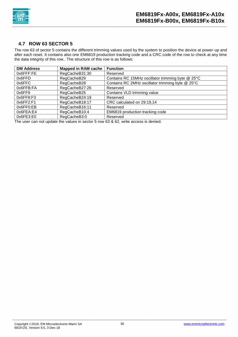
EM6819Fx-A00x, EM6819Fx-A10x EM6819Fx-B00x, EM6819Fx-B10x
Copyright 2018, EM Microelectronic-Marin SA 6819-DS, Version 9.5, 3-Dec-18
36 www.emmicroelectronic.com
4.7 ROW 63 SECTOR 5
The row 63 of sector 5 contains the different trimming values used by the system to position the device at power-up and after each reset. It contains also one EM6819 production tracking code and a CRC code of the row to check at any time the data integrity of this row.. The structure of this row is as follows:
DM Address Mapped in RAM cache Function
0x6FFF:FE RegCacheB31:30 Reserved
0x6FFD RegCacheB29 Contains RC 15MHz oscillator trimming byte @ 25°C
0x6FFC RegCacheB28 Contains RC 2MHz oscillator trimming byte @ 25°C
0x6FFB:FA RegCacheB27:26 Reserved
0x6FF9 RegCacheB25 Contains VLD trimming value
0x6FF8:F3 RegCacheB24:19 Reserved
0x6FF2:F1 RegCacheB18:17 CRC calculated on 29:19,14
0x6FF0:EB RegCacheB16:11 Reserved
0x6FEA:E4 RegCacheB10:4 EM6819 production tracking code
0x6FE3:E0 RegCacheB3:0 Reserved
The user can not update the values in sector 5 row 63 & 62, write access is denied.

EM6819Fx-A00x, EM6819Fx-A10x EM6819Fx-B00x, EM6819Fx-B10x
Copyright 2018, EM Microelectronic-Marin SA 6819-DS, Version 9.5, 3-Dec-18
37 www.emmicroelectronic.com
4.8 READ DATA IN NVM
Read access to NVM memory is done like a register read access. However only data values may be read, any access to instruction code through the data memory bus in read mode is denied. The limit between data values and instruction code is defined by the linker during compilation. As it is mentioned above, the NVM is mapped in possible data memory areas as follows:
Sector DM address (HEX)
0 0x4000 to 0x47FF
1 0x4800 to 0x4FFF
2 0x5000 to 0x57FF
3 0x5800 to 0x5FFF
4 0x6000 to 0x67FF
5 0x6800 to 0x6FFF
When NVM is accessed through the data memory bus, the execution of software is stopped during one cycle (wait state) as the data memory is shared with program memory. Reading NVM accesses always 22 bits split in three elements (2 bytes and 6bits). The two bytes are stored in a buffer; the 6 additional bits discarded. If this pair of bytes is accessed successively, the data memory buffer is read directly and the NVM is not accessed (no wait cycle).
4.9 ROW TO CACHE
When the user wants to change one byte or even one bit in the NVM, he has to write the entire row where the modification has to be done. To simplify this procedure, a sub-routine able to dump one full row to the RAM chache exists: nvm_to_cache_apl. The user has to specify the row (RegCacheCfg1) and the sector (RegCacheCfg2) pointers. After modifying the byte or the bit directly in the RAM cache he can write it’s contents back into the NVM using sub-routine write_row_apl.
Figure 4, Row to Cache flowchart
Select the row
RegCacheCfg1[5:0]
Select the sector
RegCacheCfg2[2:0]
Dump NVM row into RAM cache
Sub_routine:
nvm_to_cache_apl
Modify the RAM cache content
Write RAM cache in NVM back
Sub_routine:
write_row_apl

EM6819Fx-A00x, EM6819Fx-A10x EM6819Fx-B00x, EM6819Fx-B10x
Copyright 2018, EM Microelectronic-Marin SA 6819-DS, Version 9.5, 3-Dec-18
38 www.emmicroelectronic.com
4.9.1 NVM CONFIGURATION REGISTERS
0x02A0 RegCacheCfg1 NVM Row Cache Configuration - 1
Bits Name Type ResVal ResSrc Description
7:6 - NI - - Not implemented
5:0 CacheRow RW 0x00 ResSys NVM Row Cache: Row number of Sector (CacheSector)
0x02A1 RegCacheCfg2 NVM Row Cache Configuration - 2
Bits Name Type ResVal ResSrc Description
7 NVMFastProg RW 1 ResSys NVM fast programming mode
2:0 CacheSector RW '000' ResSys NVM Row Cache: Sector number
Note: The bit NVMFAstProg is automatically set in the ROM API routine. It is set to ‘0’ automatically when a slow operation is called, otherwise it is set to ‘1’.
0x0280 to 0x029F
RegCacheB00 to RegCacheB31
NVM Row Cache Byte-0 to NVM Row Cache Byte-31
Bits Name Type ResVal ResSrc Description
7:0 CacheB00 RW 0x00 ResSys NVM Row Cache Byte-0
… … … … …
7:0 CacheB31 RW 0x00 ResSys NVM Row Cache Byte-31

EM6819Fx-A00x, EM6819Fx-A10x EM6819Fx-B00x, EM6819Fx-B10x
Copyright 2018, EM Microelectronic-Marin SA 6819-DS, Version 9.5, 3-Dec-18
39 www.emmicroelectronic.com
5. CRC CHECK
5.1 CRC CHECK ON PROGRAM AREA
It is possible, at any time, to check the content of the NVM by calculating the CRC on the program memory. A sub-routine dedicated for this procedure exists: calc_crc_code_apl. The start and stop address of the area to check shall be given as parameter to the sub-routine as follows:
Parameter Location (CPU Index registers)
CRCStartAddrMSB r3
CRCStartAddrLSB r2
CRCStopAddrMSB r1
CRCStopAddrLSB r0
CRCStopAddr shall be higher to CRCStartAddr otherwise the routine fails and the result is not guaranteed. The full NVM memory range in program memory area is mapped as follows:
Sector PM address (HEX)
0 0x0000 to 0x03FF
1 0x0400 to 0x07FF
2 0x0800 to 0x0BFF
3 0x0C00 to 0x0FFF
4 0x1000 to 0x13FF
5 0x1400 to 0x17FF
The CRC made on program memory checks all the content of the NVM including the 6 additional bits that are not accessed through the data memory bus. Note: The user can make a CRC on the full NVM including the row 63 & 62 of sector 5. But in this case the CRC will not be constant between different devices.
5.2 CRC CHECK ON DATA AREA
It is possible, at any time, to check the content of the NVM by calculating the CRC on the data memory area. A sub-routine dedicated for this procedure exists: calc_crc_code_apl. The start and stop address of the area to check shall be given as parameter to the sub-routine as follows:
Parameter Location (CPU Index registers)
CRCStartAddrMSB r3
CRCStartAddrLSB r2
CRCStopAddrMSB r1
CRCStopAddrLSB r0
CRCStopAddr shall be higher to CRCStartAddr otherwise the routine fails and the result is not guaranteed. The full NVM memory range in data memory area is mapped as follows:
Sector DM address (HEX)
0 0x4000 to 0x47FF
1 0x4800 to 0x4FFF
2 0x5000 to 0x57FF
3 0x5800 to 0x5FFF
4 0x6000 to 0x67FF
5 0x6800 to 0x6FFF
The CRC made on data memory does not check all the content of the NVM because it excludes the 6 additional bits. It should be used to check constant tables for instance and not the program code integrity. The CRC calculation on data is also possible in the RAM area which is mapped on the following addresses:
Block DM address (HEX)
RAM 0x0080 to 0x027F
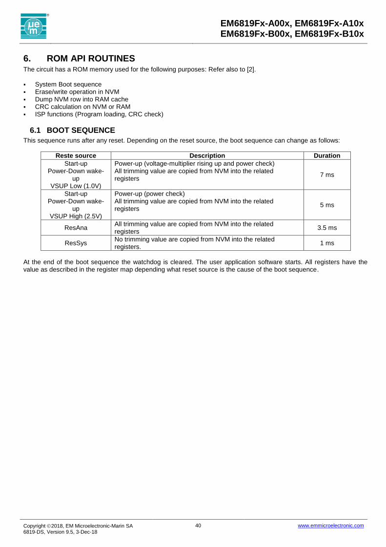
EM6819Fx-A00x, EM6819Fx-A10x EM6819Fx-B00x, EM6819Fx-B10x
Copyright 2018, EM Microelectronic-Marin SA 6819-DS, Version 9.5, 3-Dec-18
40 www.emmicroelectronic.com
6. ROM API ROUTINES The circuit has a ROM memory used for the following purposes: Refer also to [2]. System Boot sequence Erase/write operation in NVM Dump NVM row into RAM cache CRC calculation on NVM or RAM ISP functions (Program loading, CRC check)
6.1 BOOT SEQUENCE
This sequence runs after any reset. Depending on the reset source, the boot sequence can change as follows:
Reste source Description Duration
Start-up Power-Down wake-
up VSUP Low (1.0V)
Power-up (voltage-multiplier rising up and power check) All trimming value are copied from NVM into the related registers
7 ms
Start-up Power-Down wake-
up VSUP High (2.5V)
Power-up (power check) All trimming value are copied from NVM into the related registers
5 ms
ResAna All trimming value are copied from NVM into the related registers
3.5 ms
ResSys No trimming value are copied from NVM into the related registers.
1 ms
At the end of the boot sequence the watchdog is cleared. The user application software starts. All registers have the value as described in the register map depending what reset source is the cause of the boot sequence.
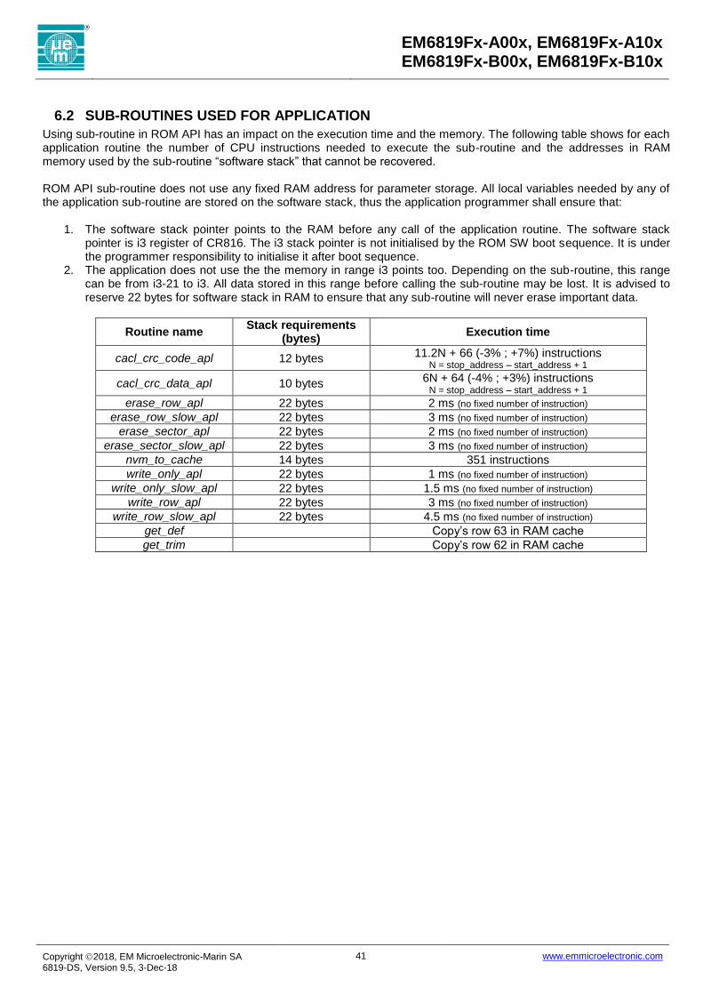
EM6819Fx-A00x, EM6819Fx-A10x EM6819Fx-B00x, EM6819Fx-B10x
Copyright 2018, EM Microelectronic-Marin SA 6819-DS, Version 9.5, 3-Dec-18
41 www.emmicroelectronic.com
6.2 SUB-ROUTINES USED FOR APPLICATION
Using sub-routine in ROM API has an impact on the execution time and the memory. The following table shows for each application routine the number of CPU instructions needed to execute the sub-routine and the addresses in RAM memory used by the sub-routine “software stack” that cannot be recovered. ROM API sub-routine does not use any fixed RAM address for parameter storage. All local variables needed by any of the application sub-routine are stored on the software stack, thus the application programmer shall ensure that:
1. The software stack pointer points to the RAM before any call of the application routine. The software stack pointer is i3 register of CR816. The i3 stack pointer is not initialised by the ROM SW boot sequence. It is under the programmer responsibility to initialise it after boot sequence.
2. The application does not use the the memory in range i3 points too. Depending on the sub-routine, this range can be from i3-21 to i3. All data stored in this range before calling the sub-routine may be lost. It is advised to reserve 22 bytes for software stack in RAM to ensure that any sub-routine will never erase important data.
Routine name Stack requirements
(bytes) Execution time
cacl_crc_code_apl 12 bytes 11.2N + 66 (-3% ; +7%) instructions N = stop_address – start_address + 1
cacl_crc_data_apl 10 bytes 6N + 64 (-4% ; +3%) instructions
N = stop_address – start_address + 1
erase_row_apl 22 bytes 2 ms (no fixed number of instruction)
erase_row_slow_apl 22 bytes 3 ms (no fixed number of instruction)
erase_sector_apl 22 bytes 2 ms (no fixed number of instruction)
erase_sector_slow_apl 22 bytes 3 ms (no fixed number of instruction)
nvm_to_cache 14 bytes 351 instructions
write_only_apl 22 bytes 1 ms (no fixed number of instruction)
write_only_slow_apl 22 bytes 1.5 ms (no fixed number of instruction)
write_row_apl 22 bytes 3 ms (no fixed number of instruction)
write_row_slow_apl 22 bytes 4.5 ms (no fixed number of instruction)
get_def Copy’s row 63 in RAM cache
get_trim Copy’s row 62 in RAM cache

EM6819Fx-A00x, EM6819Fx-A10x EM6819Fx-B00x, EM6819Fx-B10x
Copyright 2018, EM Microelectronic-Marin SA 6819-DS, Version 9.5, 3-Dec-18
42 www.emmicroelectronic.com
7. RAM RAM memory size is 512 bytes mapped in the data memory bus. It can be divided in two parts: the first part accessible with direct addressing instruction and the second part not accessible by direct addressing instructions as describe on the following table:
DM address (HEX) Addressing
0x0080 to 0x00FF Direct (128 Bytes)
0x0100 to 0x0280 Indirect (384 Bytes)
In any condition the RAM is accessed in a single CPU cycle for write and read access. Note: For any information concerning the direct and indirect addressing, refer to the CR816-DL documentation.[1]

EM6819Fx-A00x, EM6819Fx-A10x EM6819Fx-B00x, EM6819Fx-B10x
Copyright 2018, EM Microelectronic-Marin SA 6819-DS, Version 9.5, 3-Dec-18
43 www.emmicroelectronic.com
8. RESET CONTROLLER The reset controller collects all different reset sources and initializes the needed peripheral registers. Refer to the individual peripheral register mapping tables to see which reset is initializing a specific register. Some of the reset sources are maskable to prevent undesired system reinitialization. After any reset the circuit will perform a power check and go to active mode. Then the reset status bits can be read to identify the reset source.
8.1 RESET SOURCES
Possible reset source signals are: POR Power on reset, non-maskable
The fully internal POR cell will initialize the full circuit at power-up or if the supply voltge falls below VPOR voltage.
PwrDown Power-Down mode
In power down all internal registers are initialized, the pad configuration however may be locked to the last good state by setting LckPwrCfg=1 prior to Power-Down mode.
ResPA User defined Port A terminal reset function, maskable.
Any port A terminal may trigger reset. ResWD Watchdog timer reaching 0, maskable.
Logic watchdog reset running on the internal 8kHz Oscillator. ResBO Brown out reset at low regulated voltage, maskable. ResBE CoolRISC bus error when trying to access non-valid instruction space, non-maskable. ResGASP Entering Gasp modes (ISP, DoC), non-maskable.
This reset initializes the circuit prior to programming or degugging.
8.2 RESET SIGNALS
A combination of the above mentioned reset sources is used to initialize the different peripheral registers. These reset signals are POR, PorLog, ResAna, ResSys.
8.2.1 POR
A small logic remains active even in Power-Down mode to allow wake-up. This logic is initialized by POR signal. In the user data memory space this concerns the bit LckPwrCfg.
8.2.2 PORLOG
PorLog signal will reinitialize all reset flags and all pullup/pulldown configuration bits PorLog = Por OR PwrDown (logical OR combination)
8.2.3 RESANA
ResAna signal will initialize all reset enable bits, the port A input and output enable bits, the port A debouncer selection bits, all trim bits and the analog configuration settings for the DC-DC and Opamp. ResAna = Por OR PwrDown OR ResWD OR ResBE (logical OR combination)
8.2.4 RESSYS
ResSys signal initializes all remaining data memory registers, except the RAM which needs to be initialized by the user software if needed. ResSys = Por OR PwrDown OR ResWD OR ResBE OR ResPA OR ResGasp OR ResBO

EM6819Fx-A00x, EM6819Fx-A10x EM6819Fx-B00x, EM6819Fx-B10x
Copyright 2018, EM Microelectronic-Marin SA 6819-DS, Version 9.5, 3-Dec-18
44 www.emmicroelectronic.com
8.2.5 RESET FLAGS
All reset flags are in the Reset flag register: RegResFlg and placed as follows The ResFlgPA bit is asserted by reset from PortA. The ResFlgWD bit is asserted by reset from Watchdog. The ResFlgBO bit is asserted by reset from Brownout. The ResFlgGasp bit is asserted by reset from GASP. The ResFlgBE bit is asserted by reset from CoolRisc Bus-error detection. Note: To detect the Reset from Power-Down, the SW shall read the status of LckPwrCfg.
8.3 RESET REGISTERS
0x0000 RegSysCfg1 System Configuration - 1
Bits Name Type ResVal ResSrc Description
7 SelSleep RW 0 ResSys Select Sleep mode on Halt
6 SelPwrDwn RW 0 ResSys Select Power-Down mode on Halt
4 EnBrownOut RW 1 ResAna Enable Brown Out
3:2 XtalCldStart RW '00' ResSys Select Xtal Osc. ColdStart length
1 StdByFastWkUp RW 0 ResSys Stand-by mode fast Wakeup
0 VSUPLow RO 0 VSUP is Low - Tripler activated
0x0001 RegEnResPA Enable Reset by PortA bits
Bits Name Type ResVal ResSrc Description
7:0 EnResPA RW 0x00 ResAna Enable Reset by PortA bits
0x0006 RegResFlg Reset Flags
Bits Name Type ResVal ResSrc Description
7 ResFlgPA ResFlg 0 PorLog Flag Reset from Port-A
6 ResFlgWD ResFlg 0 PorLog Flag Reset from WatchDog
5 ResFlgBO ResFlg 0 PorLog Flag Reset from Brown-Out
4 ResFlgGasp ResFlg 0 PorLog Flag Reset from GASP
3 ResFlgBE ResFlg 0 PorLog Flag Reset from CoolRISC Bus-Error
0 LckPwrCfg RW 0 Por Lock configurations to be kept in Power-Down mode
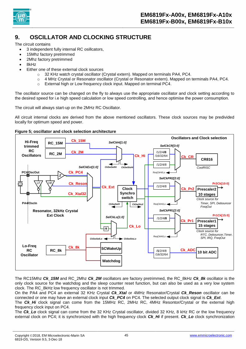
EM6819Fx-A00x, EM6819Fx-A10x EM6819Fx-B00x, EM6819Fx-B10x
Copyright 2018, EM Microelectronic-Marin SA 6819-DS, Version 9.5, 3-Dec-18
45 www.emmicroelectronic.com
9. OSCILLATOR AND CLOCKING STRUCTURE The circuit contains
3 independent fully internal RC osillcators,
15Mhz factory pretrimmed
2Mhz factory pretrimmed
8kHz
Either one of these external clock sources o 32 KHz watch crystal oscillator (Crystal extern). Mapped on terminals PA4, PC4. o 4 MHz Crystal or Resonator oscillator (Crystal or Resonator extern). Mapped on terminals PA4, PC4. o External high or Low frequency clock input. Mapped on terminal PC4.
The oscillator source can be changed on the fly to always use the appropriate oscillator and clock setting according to the desired speed for i.e high speed calculation or low speed controlling, and hence optimise the power consumption. The circuit will always start-up on the 2MHz RC Oscillator. All circuit internal clocks are derived from the above mentioned oscillators. These clock sources may be predivided locally for optimum speed and power. Figure 5; oscillator and clock selection architecture
PC4/OscOut
RC_15M
RC_2M
LF HF
Ck_ExtCk_Reson
Ck_Xtal32
Ck_15M
Ck_2M
RC_8kCk_8k
PA4/OscIn
Ck_Hi
Ck_Lo
Ck_CR
Ck_Pr2
Ck_Pr1
/4
RTC, Debouncer,Timer, SPI, IRQ, FreqOut
CoolRISC
Timer, SPI, DebouncerFreqOut
Prescaler2
10 stages
CR816
Prescaler1
15 stages
Pr1Ck[15:0]
Pr2Ck[10:0]
Watchdog
/1/2/4/8
/1/2/4/8
/1/2/4/8
/16/32/64
/1/2/4/8SelCkExt[1:0]
SelCkHi[1:0]
SelCkLo[1:0]
SelCkCR[3:0]
SelCkPR2[2:0]
SelCkPR1[2:0]
Oscillators and Clock selection
Resonator, 32kHz Crystal
Ext Clock
Hi-Freq
trimmed
RC
Oscillators
Lo-Freq
RC
Oscillator/1/2/4/8
/16/32/6410 bit ADC
Clock source for
Clock source for
Ck_ADCSCWakeUp
Ck_PC4
Clock
Synchro
switch
CkSwSelLo CkSwStsLo
CkSwSelX CkSwStsX
CkSwSelHi CkSwStsHi
ReqCkHi/Lo
ReqCkHi/Lo
ReqCkHi/Lo
The RC15Mhz Ck_15M and RC_2Mhz Ck_2M oscillators are factory pretrimmed, the RC_8kHz Ck_8k oscillator is the only clock source for the watchdog and the sleep counter reset function, but can also be used as a very low system clock. The RC_8kHz low frequency oscillator is not trimmed. On the PA4 and PC4 an external 32 KHz Crystal Ck_Xtal or 4MHz Resonator/Crystal Ck_Reson oscillator can be connected or one may have an external clock input Ck_PC4 on PC4. The selected output clock signal is Ck_Ext. The Ck_Hi clock signal can come from the 15MHz RC, 2MHz RC, 4MHz Resontor/Crystal or the external high frequency clock input on PC4. The Ck_Lo clock signal can come from the 32 KHz Crystal oscillator, divided 32 KHz, 8 kHz RC or the low frequency external clock on PC4; it is synchronized with the high frequency clock Ck_Hi if present. Ck_Lo clock synchronization

EM6819Fx-A00x, EM6819Fx-A10x EM6819Fx-B00x, EM6819Fx-B10x
Copyright 2018, EM Microelectronic-Marin SA 6819-DS, Version 9.5, 3-Dec-18
46 www.emmicroelectronic.com
with Ck_Hi allows fully synchronous circuit operation. The synchronization is disabled if the Ck_Hi or divided Ck_Hi clock is not used by any periphery. The CPU input clock Ck_CR is derived from either divided or undivided Ck_Hi or Ck_Lo. The Prescaler 1 Ck_Pr1 and Prescaler 2 CkPr2 input clock is derived fom either divided or undivided Ck_Hi or direct Ck_Lo. The ADC input clock Ck_ADC is derived from either divided or undivided Ck_Hi clock signal.
9.1 EXTERNAL CLOCK SELECTION
The External Component or Input clock source Ck_Ext is selected by register RegClockCfg1 bits SelCkExt as follows:
SelCkExt Input Used PADs Description Frequency
00 - - No clock selection none
01 Ck_Xtal PA4, PC4 Xtal 32 KHz
10 Ck_Reson PA4, PC4 Resonator 4 MHz
11 Ck_PC4 PC4, PCInpE[4]=’1’
External Clock input Used for: Ck_Hi Min: Ck_Lo * 8; Max: 15 MHz
Used for: Ck_Lo Max: Ck_Hi / 8; Min: 0 Hz
The default external clock source after system reset (ResSys) is “00” - None. The Ck_Ext clock signal is tied low. Before using an external clock input source one shall configure the necessary PA4 PC4 pads as analog inputs in case of external XTAL or Resonator, and as logic input with PCInpEn[4]=1 in case of external PC4 clock input. The external clock input on PC4 has min/max frequencies depending on its future use as Ck_Hi or Ck_Lo clock source; refer to the table above for the limits.
9.2 INTERNAL HIGH AND LOW FREQUENCY CLOCK SELECTION
The high Ck_Hi and low Ck_Low system frequencies can be selected independently but some restrictions for apply if connecting the external clock source. The High Frequency clock Ck_Hi is selected according to the register RegClockCfg1 bits SelCkHi as follows:
SelCkHi Ck_Hi Source Select signal
00 Ck_15M SelRC15M
01 Ck_2M SelRC2M
10 Ck_Ext SelExt
11 Ck_2M SelRC2M
The default Ck_Hi clock source after system reset (ResSys) is Ck_2M. The Low Frequency clock Ck_Lo is selected according to the register RegClockCfg1 bits SelCkLo as follows:
SelCkLo Ck_Lo Source Select signal
00 Ck_Ext SelExt
01 Ck_Ext Divided by 4 (Ck_Ext/4) SelExt
10 Ck_8k SelRC8k
11 Ck_8k SelRC8k
The default Ck_Lo clock source after system reset (ResSys) shall be Ck_8k. Note: If Ck_Hi or Ck_Lo are switched from external clock (SelExt active) to Ck_15M, Ck_2M or Ck_8k the SelCkExt selection must not be changed until the status bits for the selected Ck_Hi external clock RegCkSw1.CkSwStsHi or Ck_Lo external clock RegCkSw2.CkSwStsLo has changed to ‘0’

EM6819Fx-A00x, EM6819Fx-A10x EM6819Fx-B00x, EM6819Fx-B10x
Copyright 2018, EM Microelectronic-Marin SA 6819-DS, Version 9.5, 3-Dec-18
47 www.emmicroelectronic.com
9.2.1 EXTERNAL CLOCK SELECTION RESTRICTIONS
The external clock source selection for both high and low frequency clocks is very flexible, however some restrictions apply: The external clock must not be connected to both Ck_Hi and Ck_Lo at the same time. Allowed usage for external clock input on either high or low frequency domain:
External Clock source Allowed configuration
SelCkExt Source
00 None None
01 Xtal Ck_Lo: (SelCkLo == 00 || SelCkLo == 01) && SelCkHi !=10 (Ck_Hi on RC Osc and Ck_Lo on either Ck_Ext or Ck_Ext/4)
10 Renonator Ck_Hi: SelCkHi == 10 && (SelCkLo != 00 && SelCkLo != 01) (Ck_Hi on Ck_Ext and Ck_Lo on Ck_8k)
11 PC4 Ck_Lo: (SelCkLo == 00 || SelCkLo == 01) && SelCkHi !=10 (Ck_Hi on RC Osc and Ck_Lo on either Ck_Ext or Ck_Ext/4 Ck_Hi: SelCkHi == 10 && (SelCkLo != 00 && SelCkLo != 01) (Ck_Hi on Ck_Ext and Ck_Lo on Ck_8k)
9.2.2 CPU CLOCK SELECTION
The CPU input clock Ck_CR is derived from divided or undivided Ck_Hi or Ck_Lo input clock. Below table is an overview of the different CPU clocking possibilities. The CPU clock divider selection is done in register RegClockCfg2 bits SelCkCR.
SelCkCR CoolRisc Clock
0000 Ck_Hi (divided by 1)
0001 Ck_Hi divided by 2
0010 Ck_Hi divided by 4
0011 Ck_Hi divided by 8 (default)
0100 Ck_Hi divided by 16
0101 Ck_Hi divided by 32
0110 Ck_Hi divided by 64
0111 Ck_Hi divided by 8
1000 Ck_Lo (divided by 1)
1001 Ck_Lo divided by 2
1010 Ck_Lo divided by 4
1011 Ck_Lo divided by 8
1100 Ck_Lo (divided by 1)
1101 Ck_Lo (divided by 1)
1110 Ck_Lo (divided by 1)
1111 Ck_Lo (divided by 1)
The default CR clock source after system reset (ResSys) is Ck_Hi divided by 8 (selection 0x3). The CPU instruction execution cycle corresponds to half the Ck_CR clock frequency. 2 MHz input clock results in 1 MIPS. ReqCkHi or ReqCkLo signals are asserted to the Hi- or Low frequency clock switches depending of the CR multiplexer selection.

EM6819Fx-A00x, EM6819Fx-A10x EM6819Fx-B00x, EM6819Fx-B10x
Copyright 2018, EM Microelectronic-Marin SA 6819-DS, Version 9.5, 3-Dec-18
48 www.emmicroelectronic.com
9.2.3 PRESCALER1 CLOCK SELECTION
The Prescaler1 input clock Ck_Pr1 is derived from divided or undivided Ck_Hi or Ck_Lo input clock. Below table is an overview of the different prescaler1 clocking possibilities. The prescaler clock divider selection is done in register RegClockCfg3 bits SelCkPr1.
SelCkPr1 Prescaler1 Clock
000 Ck_Hi (divided by 1)
001 Ck_Hi divided by 2
010 Ck_Hi divided by 4
011 Ck_Hi divided by 8 default
100 Ck_Lo (divided by 1)
Others Ck_Hi divided by 8
The default Prescaler1 clock source after system reset (ResSys) shall be Ck_Hi divided by 8 (selection 0x3). ReqCkHi or ReqCkLo signals are asserted to the Hi- or Low frequency clock switches depending of the Prescaler1 multiplexer selection.
9.2.4 PRESCALER 2 CLOCK SELECTION
The Prescaler2 input clock Ck_Pr2 is derived from divided or undivided Ck_Hi or Ck_Lo input clock. Below table is an overview of the different prescaler1 clocking possibilities. The prescaler clock divider selection is done in register RegClockCfg3 bits SelCkPr2.
SelCkPr2 Prescaler2 Clock
000 Ck_Hi (divided by 1)
001 Ck_Hi divided by 2
010 Ck_Hi divided by 4
011 Ck_Hi divided by 8
100 Ck_Lo (divided by 1)
Others 1xx
Ck_Lo (divided by 1)
The default Prescaler2 clock source after system reset (res_sys) shall be Ck_Lo divided by 1 (selection 0x4). ReqCkHi or ReqCkLo signals are asserted to the Hi- or Low frequency clock switches depending of the Prescaler2 multiplexer selection.

EM6819Fx-A00x, EM6819Fx-A10x EM6819Fx-B00x, EM6819Fx-B10x
Copyright 2018, EM Microelectronic-Marin SA 6819-DS, Version 9.5, 3-Dec-18
49 www.emmicroelectronic.com
9.3 CLOCK CONTROL
Ck_Hi and Ck_Lo are active only if needed.
If Ck_Hi is selected by any of SelCkCR, SelCkPr1, SelCkPr2, its ReqCkHi signal becomes active and the oscillator as selected by the SelCkHi-multiplexer will be enabled, otherwise it shall be disabled. The oscillator is also enabled if forced by the corresponding FrcEn bit in register RegClockCfg2.
If Ck_Lo is selected by any of SelCkCR, SelCkPr1, SelCkPr2, its ReqCkLo signal becomes active and the oscillator as selected by the SelCkLo-multiplexer will be enabled, otherwise it shall be disabled. The oscillator is also enabled if forced by the corresponding FrcEn bit in register RegClockCfg2.
As such the oscillators are only active if there output clock is needed for either Ck_Hi or Ck_Lo. Alternatively the user may always force-on any RC oscillator and one of the external clock sources (Xtal, resonator, PC4 ext clock) Clock selection/request is provided as information which oscillator(s) are actually selected with its clock requested by a peripheral block. The request/selection bits CkSwSelX, CkSwSelHi, CkSwSelLo is high for the actual selected oscillator on the given clock switch. The coding is one-hot. Clock status information is provided to show which oscillator(s) are actually active and outputting their clock on their clock switch. The status bits CkSwStsX, CkSwStsHi, CkSwstsLo is high for the actual active oscillator on the given clock switch. The coding is one-hot. The clock selection and clock status signals are readable in register RegCkSw1 and RegCkSw2. The coding is one-hot. A selected oscillator clock is only applied to the periphery if its selection and status bit match.

EM6819Fx-A00x, EM6819Fx-A10x EM6819Fx-B00x, EM6819Fx-B10x
Copyright 2018, EM Microelectronic-Marin SA 6819-DS, Version 9.5, 3-Dec-18
50 www.emmicroelectronic.com
9.4 OSCILLATORS CONTROL
The oscillator control block assures that only the oscillators which are requested or which are forced-on are really active. The various status signals allow close monitoring of the clock switching and give essential information for power saving. Figure 6; Oscillator control architecture
PC4/OscOut
RC_15M
RC_2M
LF HF
Ck_PC4
Ck_Reson
Ck_Xtal32
Ck_15M
Ck_2M
RC_8kRC_8k
Ck_8k
PA4/OscIn
trimOsc15M
trimOsc2M
FrcEnRC15MSelRc15M
FrcEnRC2MSelRC2M
FrcEnExtOsc
SelExt
EnDCDC
SelCkExt= ‘11’
SelCkExt= ‘10’
SelCkExt=’01' StsEnXtal
StsEnReson
StsEnRC2M
StsEnRC15M
StsEnRC8k
Vreg
En En
En
Oscillator control architecture
FrcEnRC8kSelRC8k
WDDis
SleepSCStart
SCDis
Cold start
32 pulses
Cold start
progammable
8k-32k pulses
Cold start
4096
pulses
Cold start
16 pulses
Cold start
2 pulses
Cold start
4 pulsesStsCSRC15M
StsCSRC2M
StsCSPad
StsCSReson
StsCSXTAL
StsCSRc8k
EnExtPadPCInpE[4]
Oscillator availability is delayed by an individual oscillator ColdStart delay. Each disabled oscillator or external clock will go through the ColdStart phase when enabled. Following delays apply:
Oscillator ColdStart delay
RC 15 MHz 4 pulses
RC 2MHz 2 pulses
RC 8 kHz 32 pulses
Ext: from Pad 16 pulses
Ext: Resonator 4K pulses
Ext: Xtal programmable by register bits XtalCldStart
The 32 KHz Xtal ColdStart delay is programmable by the register bits XtalCldStart as follows:
RegXtalCldStart ColdStart delay
00 32K cycles (default)
01 24K cycles
10 16K cycles
11 8K cycles
The ColdStart functionality is blocking the given clock propagation to the circuit. The status of ColdStart function for each oscillator shall be readable by the register RegStsCStart bits StsCSReson, StsCSXtal, StsCSPad, StsCSRC8k, StsCSRC2M, StsCSRC15M.

EM6819Fx-A00x, EM6819Fx-A10x EM6819Fx-B00x, EM6819Fx-B10x
Copyright 2018, EM Microelectronic-Marin SA 6819-DS, Version 9.5, 3-Dec-18
51 www.emmicroelectronic.com
The oscillator Force-On functionality can be used to avoid recurrent coldstart delays on fast clock switching. An Oscillator is enabled if its clock is requested by either of the SelCkCR, SelCkPr1, SelCkPr2 clock selection bits or forced-on by register RegClockCfg2 bits FrcEnXXX as follows:
Oscillator Condition Status bit
RC15 MHz SelRC15M || FrcEnRC15M || EnDC-DC StsEnRC15M
RC2 MHz SelRC2M || FrcEnRC2M StsEnRC2M
Xtal (SelExt || FrcEnExt) && SelCkExt=”01” StsEnXtal
Resonator (SelExt || FrcEnExt) && SelCkExt=”10” StsEnReson
The oscillator enable signals are readable by the register RegStsEnOsc bits StsEnReson, StsEnXtal, StsEnRC8k, StsEnRC2M, StsEnRC15M. An External clock Source from pad PC4 is enabled if selected or forced-on by register RegClockCfg2 bit FrcEnExt , its status is read on StsCSPad: StsCSPad = (SelExt || FrcEnExt) && SelCkExt=”11” PCInpE[4] must be high to allow PC4 clock input The RC 15 MHz oscillator is always automatically enabled if the DC-DC converter is switched on (register RegDC-DCCfg bit EnDC-DC). The oscillators (except RC_8K) and the external clock sources are automatically disabled in Sleep mode. This has priority over Select and Force-On functionality. The oscillators and the external clock sources are automatically disabled by power-check functionality. This has priority over Select and Force-On functionality. The RC 8 kHz oscillator is enabled
in Sleep mode with active sleepcounter function if the watchdog is enabled, if requested by any of the SelCkCR, SelCkPr1 and SelCkPr2 clock selection and when forced-on.
The status bit of the RC_8k is readable in register RegStsEnOsc bit StsEnRC8k StsEnRC8k = FrcEnRC8k || SelRC8k || ((Sleep || SCStart) && !SCDis) || !WDDis Note: The RC_8kHz oscillator can only be disabled at least 300us after its coldstart. ( RegStsCStart.StsCSRC8k)

EM6819Fx-A00x, EM6819Fx-A10x EM6819Fx-B00x, EM6819Fx-B10x
Copyright 2018, EM Microelectronic-Marin SA 6819-DS, Version 9.5, 3-Dec-18
52 www.emmicroelectronic.com
9.5 CLOCK CONTROL REGISTERS
0x0000 RegSysCfg1 System Configuration - 1
Bits Name Type ResVal ResSrc Description
7 SelSleep RW 0 ResSys Select Sleep mode on Halt
6 SelPwrDwn RW 0 ResSys Select Power-Down mode on Halt
4 EnBrownOut RW 1 ResAna Enable Brown Out
3:2 XtalCldStart RW '00' ResSys Select Xtal Osc. ColdStart length
1 StdByFastWkUp RW 0 ResSys Stand-by mode fast Wakeup
0 VSUPLow RO 0 VSUP is Low - Tripler activated
0x0003 RegClockCfg1 Clock Configuration - 1
Bits Name Type ResVal ResSrc Description
7:6 SelCkExt RW_Res '00' ResSys Select External Component/Input clock source
5:4 SelCkHi RW_Res '01' ResSys Select High freq. Clock source
3:2 SelCkLo RW_Res '10' ResSys Select Low freq. Clock source
1 - NI - - Not implemented
0 FrcFastRead RW 0 ResSys Force NVM Fast Read
0x0004 RegClockCfg2 Clock Configuration - 2
Bits Name Type ResVal ResSrc Description
7 FrcEnRC15M RW 0 ResSys Force 15 MHz RC Oscillator ON
6 FrcEnRC2M RW 0 ResSys Force 2 MHz RC Oscillator ON
5 FrcEnRC8k RW 0 ResSys Force 8 kHz RC Oscillator ON
4 FrcEnExt RW 0 ResSys Force selected (SelCkExt) External Component/Input clock source ON
3:0 SelCkCR RW_Res 0x3 ResSys Select CoolRisc/CPU Clock source
0x0005 RegClockCfg3 Clock Configuration - 3
Bits Name Type ResVal ResSrc Description
7:5 SelCkPr1 RW_Res '011' ResSys Select Prescaler1 Clock source
4:2 SelCkPr2 RW_Res '100' ResSys Select Prescaler2 Clock source
1:0 - NI - - -
0x02A5 RegStsCStart Ostcillators ColdStart Status
Bits Name Type ResVal ResSrc Description
7:6 - NI - - -
5 StsCSReson RO 1 ResSys ColdStart Status of (4 MHz) Resonator Oscillator
4 StsCSXtal RO 1 ResSys ColdStart Status of (32K Hz) Xtal Oscillator
3 StsCSPad RO 1 ResSys ColdStart Status of External Pad-Clock
2 StsCSRC8k RO 0 ResSys ColdStart Status of 8 kHz RC Oscillator
1 StsCSRC2M RO 0 ResSys ColdStart Status of 2 MHz RC Oscillator
0 StsCSRC15M RO 1 ResSys ColdStart Status of 15 MHz RC Oscillator
0x02A6 RegStsEnOsc Ostcillators Enable Status
Bits Name Type ResVal ResSrc Description
7:5 - NI - - Not implemented
4 StsEnReson RO 0 ResSys Enabled Status/State of (4 MHz) Resonator Oscillator
3 StsEnXtal RO 0 ResSys Enabled Status/State of (32K Hz) Xtal Oscillator
2 StsEnRC8k RO 1 ResSys Enabled Status/State of 8 kHz RC Oscillator
1 StsEnRC2M RO 1 ResSys Enabled Status/State of 2 MHz RC Oscillator
0 StsEnRC15M RO 0 ResSys Enabled Status/State of 15 MHz RC Oscillator

EM6819Fx-A00x, EM6819Fx-A10x EM6819Fx-B00x, EM6819Fx-B10x
Copyright 2018, EM Microelectronic-Marin SA 6819-DS, Version 9.5, 3-Dec-18
53 www.emmicroelectronic.com
0x02A7 RegCkSw1 Clock switches Selector/Request and current Status - 1
Bits Name Type ResVal ResSrc Description
7 CkSwSelX RO 0 ResSys Ck_SW Clock (Ck-Hi/Ck-Lo) Sync. clock switch Selector/Request Status ‘1’ - CK_Lo, ‘0’ - CK_Hi
6 CkSwStsX RO 0 ResSys Ck_SW Clock (Ck-Hi/Ck-Lo) Sync. clock switch current Status ‘1’ - CK_Lo, ‘0’ - CK_Hi
5:3 CkSwSelHi RO '010' ResSys Ck-Hi Clock switch (one-hot) Selector/Request Status bit0 – Ck_15M, Bit1 – Ck_2M, bit2 – Ck_Ext
2:0 CkSwStsHi RO '010' ResSys Ck-Hi Clock switch (one-hot) current Status bit0 – Ck_15M, Bit1 – Ck_2M, bit2 – Ck_Ext
0x02A8 RegCkSw2 Clock switches Selector/Request and current Status - 2
Bits Name Type ResVal ResSrc Description
7:6 - NI - - Not implemented
5:3 CkSwSelLo RO '100' ResSys Ck-Lo Clock switch (one-hot) Selector/Request Status bit0 – Ck_Ext, Bit1 – Ck_Ext/4, bit2 – Ck_8k
2:0 CkSwStsLo RO '100' ResSys Ck-Lo Clock switch (one-hot) current Status bit0 – Ck_Ext, Bit1 – Ck_Ext/4, bit2 – Ck_8k

EM6819Fx-A00x, EM6819Fx-A10x EM6819Fx-B00x, EM6819Fx-B10x
Copyright 2018, EM Microelectronic-Marin SA 6819-DS, Version 9.5, 3-Dec-18
54 www.emmicroelectronic.com
10. PRESCALER1 The prescaler1 is a 15 stage clock divider. It is typically used to deliver the input clocks to the digital peripherals (timers, SPI, etc..). Its last stage output is on 1Hz (at 32768Hz input clock) and therefore most often used to construct a RTC (Real Time Clock) system. It can also be used as a free running counter by reading the current status of Pr1Ck0(MSB) to Pr1Ck7(LSB) in register RegPresc1Val.
10.1 PRESCALER1 CLOCK SELECTION
The Prescaler1 input clock Ck_Pr1 is derived from divided or undivided Ck_Hi or Ck_Lo input clock. Below table is an overview of the different prescaler1 clocking possibilities. The prescaler clock divider selection is done in register RegClockCfg3 bits SelCkPr1.
SelCkPr1 Prescaler1 Clock
000 Ck_Hi (divided by 1)
001 Ck_Hi divided by 2
010 Ck_Hi divided by 4
011 Ck_Hi divided by 8 (default)
100 Ck_Lo (divided by 1)
Others Ck_Hi divided by 8
The default Prescaler1 clock source after system reset (ResSys) shall be Ck_Hi divided by 8 (selection 0x3). It is possible to run the 15 stage precaler1 on 13 stages only. This is typically used when connecting the RC_8K oscillator as the prescaler1 clock source and allow to keep the nominal prescaler output frequencies as if there would be an 32kHz Xtal oscillator connected (prescaler at 15 stages). The prescaler1 length selection is done in register RegPrescCfg bit Presc1Len (‘0’= 15 stages, ‘1’=13 stages). The Signals Pr1Ck14 and Pr1Ck13 are thus not influenced by the shortening. Assuming a Prescaler1 with N stages, then the signal Pr1Ck[N] is the input of the first stage, Pr1Ck[N-1] is the output of the first stage (input divided by 2) and Pr1Ck0 is the output of the last stage (the lowest frequency). This leads to following clock source name definitions.
Prescaler1 stage
Clock Name Presc1Len = ‘0’ Presc1Len = ‘1’
Division by Fout Division by Fout
Prescaler source: Pr1Ck15 1 2^0 32K 1 2^0 8K
Stage 1 Pr1Ck14 2 2^1 16K 2 2^1 4K
Stage 2 Pr1Ck13 4 2^2 8K 4 2^2 2K
Stage 3 Pr1Ck12 8 2^3 4K 2 2^1 4K
Stage 4 Pr1Ck11 16 2^4 2K 4 2^2 2K
Stage 5 Pr1Ck10 32 2^5 1K 8 2^3 1K
Stage 6 Pr1Ck9 64 2^6 512 16 2^4 512
Stage 7 Pr1Ck8 128 2^7 256 32 2^5 256
Stage 8 Pr1Ck7 256 2^8 128 64 2^6 128
Stage 9 Pr1Ck6 512 2^9 64 128 2^7 64
Stage 10 Pr1Ck5 1K 2^10 32 256 2^8 32
Stage 11 Pr1Ck4 2K 2^11 16 512 2^9 16
Stage 12 Pr1Ck3 4K 2^12 8 1K 2^10 8
Stage 13 Pr1Ck2 8K 2^13 4 2K 2^11 4
Stage 14 Pr1Ck1 16K 2^14 2 4K 2^12 2
Stage 15 Pr1Ck0 32K 2^15 1 8K 2^13 1
The frequencies Fout given in this table are based on 32 KHz clock selection as a prescaler1 input source.

EM6819Fx-A00x, EM6819Fx-A10x EM6819Fx-B00x, EM6819Fx-B10x
Copyright 2018, EM Microelectronic-Marin SA 6819-DS, Version 9.5, 3-Dec-18
55 www.emmicroelectronic.com
10.2 PRESCALER1 RESET
Writing ‘1’ to the bit Presc1Clr in register RegPrescCfg sets all stages to ‘1’ and counting restarts.
10.2.1.1 PRESCALER1 INTERRUPT GENERATION
The prescaler1 generates 2 interrupt signals
IntPr1Ck0 interrupt signal is generated on the stage 15 overrun (rising Pr1Ck0 edge)
IntPr1Ck5/3 interrupt signal is generated on the stage 10 or stage12 overrun (rising Pr1Ck3 or Pr1Ck5 edge). The selection is done in register PrescCfg bit Presc1SelIntck5/3 as follows:
Presc1SelIntck5/3 Int. Freq. (based on 32KHz) Pr1-Ck
0 (Default) 8 Hz Pr1Ck3
1 32 Hz Pr1Ck5
The frequencies given in this table are based on 32 KHz clock selection as a prescaler1 input source.
10.3 PRESCALER REGISTERS
0x0007 RegPrescCfg Prescaler-1/2 Configuration
Bits Name Type ResVal ResSrc Description
7 Presc1Clr OS 0 Prescaler-1 Clear counter
6 Presc1Len RW 0 ResSys Prescaler-1 Length
5 Presc1SelIntck5/3 RW 0 ResSys Select Prescaler-1 irq-B source: 0-8Hz, 1-32Hz
4 Presc2Clr OS 0 Prescaler-2 Clear counter
3:0 - NI - - Not implemented
0x0008 RegPresc1Val Prescaler-1 Value (MSB)
Bits Name Type ResVal ResSrc Description
7:0 Presc1Val RO 0xFF ResSys Prescaler-1 Value (MSB) , Pr1Ck0 to Pr1Ck7 status

EM6819Fx-A00x, EM6819Fx-A10x EM6819Fx-B00x, EM6819Fx-B10x
Copyright 2018, EM Microelectronic-Marin SA 6819-DS, Version 9.5, 3-Dec-18
56 www.emmicroelectronic.com
11. PRESCALER2 The prescaler2 is a 10 stage clock divider. It is typically used to deliver the input clocks to the digital peripherals (timers, SPI, etc. It can also be used as a free running counter by reading the current status of Pr2Ck0(MSB) to Pr2Ck7(LSB) in register RegPresc2Val.
11.1 PRESCALER2 CLOCK SELECTION
The Prescaler2 input clock Ck_Pr2 is derived from divided or undivided Ck_Hi or Ck_Lo input clock. Below table is an overview of the different prescaler1 clocking possibilities. The prescaler clock divider selection is done in register RegClockCfg3 bits SelCkPr2.
SelCkPr2 Prescaler2 Clock
000 Ck_Hi (divided by 1)
001 Ck_Hi divided by 2
010 Ck_Hi divided by 4
011 Ck_Hi divided by 8
100 Ck_Lo (divided by 1)
Others Ck_Lo (divided by 1)
The default Prescaler-2 clock source after system reset (res_sys) shall be Ck_Lo divided by 1 (selection 0x4). Assuming a Prescaler2 with N stages, then the signal Pr2ck[N] is the input of the first stage, Pr2Ck[N-1] is the output of the first stage (input divided by 2) and Pr2Ck0 is the output of the last stage (the lowest frequency). This leads to following clock source name definitions.
Prescaler2 stage
Clock Name Division by Fout
Prescaler source: Pr2Ck10 1 2^0 2 M
Stage 1 Pr2Ck9 2 2^1 1 M
Stage 2 Pr2Ck8 4 2^2 500 k
Stage 3 Pr2Ck7 8 2^3 250 k
Stage 4 Pr2Ck6 16 2^4 125 k
Stage 5 Pr2Ck5 32 2^5 62500
Stage 6 Pr2Ck4 64 2^6 31250
Stage 7 Pr2Ck3 128 2^7 15625
Stage 8 Pr2Ck2 256 2^8 7812.5
Stage 9 Pr2Ck1 512 2^9 3906.25
Stage 10 Pr2Ck0 1K 2^10 1953.125
The frequencies Fout given in this table are based on 32 KHz clock selection as a prescaler2 input source.
11.2 PRESCALER2 RESET
Writing ‘1’ to the bit Presc2Clr in register RegPrescCfg sets all stages to ‘1’ and counting restarts.
11.3 PRESCALER2 REGISTERS
0x0007 RegPrescCfg Prescaler-1/2 Configuration
Bits Name Type ResVal ResSrc Description
7 Presc1Clr OS 0 Prescaler-1 Clear counter
6 Presc1Len RW 0 ResSys Prescaler-1 Length
5 Presc1SelIntck5/3 RW 0 ResSys Select Prescaler-1 irq-B source: 0-8Hz, 1-32Hz
4 Presc2Clr OS 0 Prescaler-2 Clear counter
3:0 - NI - - Not implemented
0x0009 RegPresc2Val Prescaler-2 Value (MSB)
Bits Name Type ResVal ResSrc Description
7:0 Presc2Val RO 0xFF ResSys Prescaler-2 Value (MSB), Pr2Ck0 to Pr2Ck7 status

EM6819Fx-A00x, EM6819Fx-A10x EM6819Fx-B00x, EM6819Fx-B10x
Copyright 2018, EM Microelectronic-Marin SA 6819-DS, Version 9.5, 3-Dec-18
57 www.emmicroelectronic.com
12. INTERRUPT AND EVENT CONTROLLER
12.1 INTERRUPTS GENERAL
12.1.1 BASIC FEATURES
The circuit handles 24 independent Interrupt sources grouped into 3 priority levels.
Highest Priority : Level 0 : Prescaler1, PmMiss, GASP, ADC, Timer, Ports
Medium Priority : Level 1 : SPI, Prescaler1, OpAmp, Timer, Ports
Lowest Priority : Level 2 : Timer, Ports, Sleep counter, VLD As such the circuit contains
13 external Interrupts (Ports, SPI, OpAmp, VLD, GASP)
12 internal Interrupts (Prescaler, DoC, Timer, SPI, PmMiss, Sleep Counter) Interrupt from SPI and Timer may be initialized by either external or internal actions (i.e. timer running on external clock) Interrupts force a CALL to a fixed interrupt vector, save the program counter (PC) onto the hardware stack and reset the general interrupt bit (GIE). If the CPU was in StandBy mode prior to Interrupt then it will come back in active mode. Each priority level has its own interrupt vector.
Level 1 sets bit IN1 in CoolRISC status register Program memory address 1 Call Vector 1
Level 2 sets bit IN2 in CoolRISC status register Program memory address 2 Call Vector 2
Level 0 sets bit IN0 in CoolRISC status register Program memory address 3 Call Vector 0 The GIE bit is restored when returning from interrupt with the RETI instruction. The RET instruction does not reinstall the GIE. Nested interrupts are possible by re-enabling the GIE bit within the interrupt routine. Functions such as interrupt Pre- or Post-masking, enabling and clearing are available on different levels in the interrupt structure. At power up or after any reset all interrupt inputs are masked and the GIE is cleared. The Interrupt handling is split into 2 parts.
One part deals with the acquisition, masking and clearing of the interrupts outside of the CPU. Interrupt acquisition, IRQ Controller
The 2nd part covers all aspects of priority and interrupts enabling inside the CoolRISC core. CPU interrupts handling
Figure 7, Interrupt top level diagram
Interrupt
Controller
Interrupt
acquisition
CPU
CR816
Interrupt handling
CPUInt0
CPUInt1
R/W Control
Level 0
Interrupt
sources 8
CPUInt2
RegInt0Sts
RegInt1Sts
RegInt2Sts
IN0
IN1
IN2Level 1
Interrupt
sources 8
Level 2
Interrupt
sources 8
Interrupt Diagram

EM6819Fx-A00x, EM6819Fx-A10x EM6819Fx-B00x, EM6819Fx-B10x
Copyright 2018, EM Microelectronic-Marin SA 6819-DS, Version 9.5, 3-Dec-18
58 www.emmicroelectronic.com
12.2 INTERRUPT ACQUISITION
A positive edge on any of the unmasked interrupt source signals will set the corresponding interrupt register bit and activate the mapped CPU interrupt input. (I.e. Timer3 interrupt IntTim3 will set bit Int1StsTim3 in register RegInt1Sts and activate the CPUInt1 interrupt input if mask bit Int1MskTim3 is ‘1’ [non-masked] ). The 3 priority branches for interrupt acquisition are totally independent of each other, masking and selective clear of interrupts on one interrupt vector input does not modify the others. All Interrupts inputs are available in active and standby mode. Table 1. Interrupts signal sources and destination
Interrupt
sources
Int
vectorMapping remark
Sleep wake-
up
IntPort0 Int0StsPort0 PA0 or PC0, positive and/or negative edge X (PA)
IntTim1 Int0StsTim1 Timer1 Input capture, Compare value, Compare Full
IntPr1Ck0 Int0StsPrCk0 Prescaler1 1Hz (Pr1Ck0)
IntADC Int0StsADC ADC conversion finished
IntDoCDM Int0StsDoCDM DoC data memory address match
IntDoCPM Int0StsDoCPM DoC program memory address match
IntGASP Int0StsGASP GASP data reception with sign='1' X
IntPmMiss Int0StsPmMiss Program memory, wait introduction
IntPort2 Int1StsPort2 PA2 or PC2, positive and/or negative edge X (PA)
IntPort1 Int1StsPort2 PA1 or PC1, positive and/or negative edge X (PA)
IntTim2 Int1StsTim2 Timer2, Input capture, Compare value, Compare Full
IntTim3 Int1StsTim3 Timer3, Input capture, Compare value, Compare Full
IntOpAmp Int1StsOpAmp Comparator; falling and/or rising output change X
IntPr1Ck5/3 Int1StsPr1Ck5/3 Prescaler 1, 8Hz or 32Hz (falling edge)
IntSPIStop Int1StsSPIStop SPI, Stop transmission 1 byte
IntSPIStart Int1StsSPIStart SPI, Start transmission 1byte
IntVLD Int2StsVLD Voltage level detector; input low X
IntSlpCnt Int2StsSlpCnt Sleep counter wakeup timeout X
IntPort7 Int2StsPort7 PA7 or PC7, positive and/or negative edge X (PA)
IntPort6 Int2StsPort6 PA6 or PC6, positive and/or negative edge X (PA)
IntPort5 Int2StsPort5 PA5 or PC5, positive and/or negative edge X (PA)
IntPort4 Int2StsPort4 PA4 or PC4, positive and/or negative edge X (PA)
IntPort3 Int2StsPort3 PA3 or PC3, positive and/or negative edge X (PA)
IntTim4 Int2StsTim4 Timer4, Input capture, Compare value, Compare Full
0
1
2
The following interrupt sources can wake-up the device from the Sleep mode if enabled by appropriate interrupt masks: Table 2. Wake-Up Interrupts
Interrupt Source Interrupt Status
PortA; regardless of RegIntPortSrc IntXStsPort7 to IntXStsPort0
Sleep counter Int2StsSlpCnt
SVLD Int2StsVLD
OpAmp Int1StsOpAmp
GASP Int0StsGASP Direct (non-debounced) port A interrupts are, used for the wake-up, totaly independent of the debouncer settings.

EM6819Fx-A00x, EM6819Fx-A10x EM6819Fx-B00x, EM6819Fx-B10x
Copyright 2018, EM Microelectronic-Marin SA 6819-DS, Version 9.5, 3-Dec-18
59 www.emmicroelectronic.com
12.3 INTERRUPTS FROM IO PORTS
The register RegIntPortSrc selects the port interrupt source IntPort coming from port A or port C in Active and StandBy modes. In Sleep mode, the port A is always selected independent of RegIntPortSrc settings.
If RegIntPortSrc[X] = ‘0’ then IntPort[X] source shall be IntPA[X] otherwise it is IntPC[X].
The default value of RegIntPortSrc is 0x00, i.e. IntPA[X] is selected.
12.4 INTERRUPT ACQUISITION MASKING.
At start up or after any reset all interrupt sources are masked (mask bits are ‘0’). To activate a specific interrupt source input the corresponding mask bit must be set ‘1’. Masking does not clear an existing interrupt but will prevent future interrupts on the same input. Refer to Figure 8, Interrupt acquisition architecture.
12.4.1 PRE AND POSTMASKING OF INTERRUPTS
One pair of registers for each level of priority RegIntXMsk and RegIntXPostMsk control the interrupt generation for CPU and catch an incoming request into the status registers RegIntXSts as follows:
If RegIntXMsk[Y] =’1’ then the appropriate CPU interrupt line IntX is asserted and interrupt is caught in the status register RegIntXSts[Y].
If RegIntXMsk[Y] =’0’ then the appropriate CPU interrupt line IntX is NOT asserted. The interrupt request is caught in the status register RegIntXSts[Y] only if RegIntXPostMsk[Y] =’1’.
If RegIntXMsk[Y] =’0’ then the appropriate CPU interrupt line IntX is NOT asserted. The interrupt request is NOT caught in the status register RegIntXSts[Y] if RegIntXPostMsk[Y] =’0’.
Figure 8, Interrupt acquisition architecture
Int0[8:0]
CPUInt0
8
8
8
Int0PostMsk
Int0Msk
Q
QSET
CLR
D
8
IntPort0
IntTim1
IntPr1Ck0
IntADC
IntDoCDM
IntDocPM
IntGASP
IntPmMiss 0
1
2
3
4
5
6
7
Int1[8:0]
CPUInt1
8
8
8
Int1PostMsk
Int1Msk
Q
QSET
CLR
D
8
IntPort2
IntPort1
IntTim2
IntTim3
IntOpAmp
IntPr1Ck5/3
IntSPIStop
IntSPIStart 0
1
2
3
4
5
6
7
Int2[8:0]
CPUInt2
8
8
8
Int2PostMsk
Int2Msk
Q
QSET
CLR
D
8
IntVLD
IntSlpCnt
IntPort7
IntPort6
IntPort5
IntPort4
IntPort3
IntTim4 0
1
2
3
4
5
6
7
D
En
QD
Ck
Q
SW write ‘1’
to IntXSts bit
SW write ‘1’
to IntXSts bit
SW read
RegIntXSts
To DatabusIntXSts
IntXMsk
IntXPostMask
INV
Interrupt aquisition
IntXSource
Int0Source
Int1Source
Int2Source
IntX
Int0Sts[8:0]
Int1STS[8:0]
Int2STS[8:0]

EM6819Fx-A00x, EM6819Fx-A10x EM6819Fx-B00x, EM6819Fx-B10x
Copyright 2018, EM Microelectronic-Marin SA 6819-DS, Version 9.5, 3-Dec-18
60 www.emmicroelectronic.com
12.5 INTERRUPT ACQUISITION CLEARING
A pending interrupt can be cleared in 3 ways
Reading the interrupt registers RegInt0Sts, RegInt1Sts and RegInt2Sts will automatically clear all stored interrupts which were set prior to the read in the corresponding register. This read is normally done inside the interrupt subroutine to determine the source of the interrupt.
Each interrupt request status bit can be individually cleared (set ‘0’) by writing ‘0’ to the corresponding RegInt0Sts, RegInt1Sts and RegInt2Sts register bit. Software clearing of the interrupt status bit has priority over an incoming interrupt.
At power up or after any reset all interrupt registers are reset.
12.5.1 SOFTWARE INTERRUPT ACQUISITION SET
Each interrupt request status bit can be individually set (set ‘1’) by writing ‘1’ to the corresponding RegInt0Sts, RegInt1Sts and RegInt2Sts register bit. Write ‘1’ has the highest priority on the status bit.
12.6 INTERRUPT REGISTERS
0x0061 RegInt0Sts Interrupt level-0 Status
Bits Name Type ResVal ResSrc Description
7 Int0StsPort(0) RW-INT 0 ResSys Interrupt level-0 Status - Port(0)
6 Int0StsTim1 RW-INT 0 ResSys Interrupt level-0 Status - Timer-1
5 Int0StsPr1Ck0 RW-INT 0 ResSys Interrupt level-0 Status - Prescaler1 Ck0 (1Hz)
4 Int0StsADC RW-INT 0 ResSys Interrupt level-0 Status - ADC
3 Int0StsDoCDM RW-INT 0 ResSys Interrupt level-0 Status - DoC DM
2 Int0StsDoCPM RW-INT 0 ResSys Interrupt level-0 Status - DoC PM
1 Int0StsGASP RW-INT 0 ResSys Interrupt level-0 Status - GASP
0 Int0StsPmMiss RW-INT 0 ResSys Interrupt level-0 Status - PM_Miss
0x0062 RegInt1Sts Interrupt level-1 Status
Bits Name Type ResVal ResSrc Description
7 Int1StsPort(2) RW-INT 0 ResSys Interrupt level-1 Status - Port(2)
6 Int1StsPort(1) RW-INT 0 ResSys Interrupt level-1 Status - Port(1)
5 Int1StsTim2 RW-INT 0 ResSys Interrupt level-1 Status - Timer-2
4 Int1StsTim3 RW-INT 0 ResSys Interrupt level-1 Status - Timer-3
3 Int1StsOpAmp RW-INT 0 ResSys Interrupt level-1 Status - OpAmp
2 Int1StsPr1Ck5/3 RW-INT 0 ResSys Interrupt level-1 Status – Prescaler1 Ck5 or Ck3
1 Int1StsSPIStop RW-INT 0 ResSys Interrupt level-1 Status - SPI_Stop
0 Int1StsSPIStart RW-INT 0 ResSys Interrupt level-1 Status - SPI_Start
0x0063 RegInt2Sts Interrupt level-2 Status
Bits Name Type ResVal ResSrc Description
7 Int2StsVLD RW-INT 0 ResSys Interrupt level-2 Status - VLD
6 Int2StsSlpCnt RW-INT 0 ResSys Interrupt level-2 Status - Sleep Counter
5 Int2StsPort(7) RW-INT 0 ResSys Interrupt level-2 Status - Port(7)
4 Int2StsPort(6) RW-INT 0 ResSys Interrupt level-2 Status - Port(6)
3 Int2StsPort(5) RW-INT 0 ResSys Interrupt level-2 Status - Port(5)
2 Int2StsPort(4) RW-INT 0 ResSys Interrupt level-2 Status - Port(4)
1 Int2StsPort(3) RW-INT 0 ResSys Interrupt level-2 Status - Port(3)
0 Int2StsTim4 RW-INT 0 ResSys Interrupt level-2 Status - Timer-4

EM6819Fx-A00x, EM6819Fx-A10x EM6819Fx-B00x, EM6819Fx-B10x
Copyright 2018, EM Microelectronic-Marin SA 6819-DS, Version 9.5, 3-Dec-18
61 www.emmicroelectronic.com
0x0064 RegInt0Msk Interrupt level-0 Mask
Bits Name Type ResVal ResSrc Description
7 Int0MskPort(0) RW 0 ResSys Interrupt level-0 Mask - Port(0)
6 Int0MskTim1 RW 0 ResSys Interrupt level-0 Mask - Timer-1
5 Int0MskPr1Ck0 RW 0 ResSys Interrupt level-0 Mask - Prescaler1 1Hz
4 Int0MskADC RW 0 ResSys Interrupt level-0 Mask - ADC
3 Int0MskDoCDM RW 0 ResSys Interrupt level-0 Mask - DoC DM
2 Int0MskDoCPM RW 0 ResSys Interrupt level-0 Mask - DoC PM
1 Int0MskGASP RW 0 ResSys Interrupt level-0 Mask - GASP
0 Int0MskPmMiss RW 0 ResSys Interrupt level-0 Mask - PM_Miss
0x0065 RegInt1Msk Interrupt level-1 Mask
Bits Name Type ResVal ResSrc Description
7 Int1MskPort(2) RW 0 ResSys Interrupt level-1 Mask - Port(2)
6 Int1MskPort(1) RW 0 ResSys Interrupt level-1 Mask - Port(1)
5 Int1MskTim2 RW 0 ResSys Interrupt level-1 Mask - Timer-2
4 Int1MskTim3 RW 0 ResSys Interrupt level-1 Mask - Timer-3
3 Int1MskOpAmp RW 0 ResSys Interrupt level-1 Mask - OpAmp
2 Int1MskPr1Ck5/3 RW 0 ResSys Interrupt level-1 Mask - Prescaler1 Ck5 or Ck3
1 Int1MskSPIStop RW 0 ResSys Interrupt level-1 Mask - SPI_Stop
0 Int1MskSPIStart RW 0 ResSys Interrupt level-1 Mask - SPI_Start
0x0066 RegInt2Msk Interrupt level-2 Mask
Bits Name Type ResVal ResSrc Description
7 Int2MskVLD RW 0 ResSys Interrupt level-2 Mask - VLD
6 Int2MskSlpCnt RW 0 ResSys Interrupt level-2 Mask - Sleep Counter
5 Int2MskPort(7) RW 0 ResSys Interrupt level-2 Mask - Port(7)
4 Int2MskPort(6) RW 0 ResSys Interrupt level-2 Mask - Port(6)
3 Int2MskPort(5) RW 0 ResSys Interrupt level-2 Mask - Port(5)
2 Int2MskPort(4) RW 0 ResSys Interrupt level-2 Mask - Port(4)
1 Int2MskPort(3) RW 0 ResSys Interrupt level-2 Mask - Port(3)
0 Int2MskTim4 RW 0 ResSys Interrupt level-2 Mask - Timer-4
0x0067 RegInt0PostMsk Interrupt level-0 Post_Mask
Bits Name Type ResVal ResSrc Description
7 Int0PostMskPort(0) RW 0 ResSys Interrupt level-0 Post_Mask - Port(0)
6 Int0PostMskTim1 RW 0 ResSys Interrupt level-0 Post_Mask - Timer-1
5 Int0PostMskPr1Ck0 RW 0 ResSys Interrupt level-0 Post_Mask - Prescaler1 1Hz
4 Int0PostMskADC RW 0 ResSys Interrupt level-0 Post_Mask - ADC
3 Int0PostMskDoCDM RW 0 ResSys Interrupt level-0 Post_Mask - DoC DM
2 Int0PostMskDoCPM RW 0 ResSys Interrupt level-0 Post_Mask - DoC PM
1 Int0PostMskGASP RW 0 ResSys Interrupt level-0 Post_Mask - GASP
0 Int0PostMskPmMiss RW 0 ResSys Interrupt level-0 Post_Mask - PM_Miss
0x0068 RegInt1PostMsk Interrupt level-1 Post_Mask
Bits Name Type ResVal ResSrc Description
7 Int1PostMskPort(2) RW 0 ResSys Interrupt level-1 Post_Mask - Port(2)
6 Int1PostMskPort(1) RW 0 ResSys Interrupt level-1 Post_Mask - Port(1)
5 Int1PostMskTim2 RW 0 ResSys Interrupt level-1 Post_Mask - Timer-2
4 Int1PostMskTim3 RW 0 ResSys Interrupt level-1 Post_Mask - Timer-3
3 Int1PostMskOpAmp RW 0 ResSys Interrupt level-1 Post_Mask - OpAmp
2 Int1PostMskPr1Ck5/3 RW 0 ResSys Interrupt level-1 Post_Mask - Prescaler1 Ck5 or Ck3
1 Int1PostMskSPIStop RW 0 ResSys Interrupt level-1 Post_Mask - SPI_Stop
0 Int1PostMskSPIStart RW 0 ResSys Interrupt level-1 Post_Mask - SPI_Start

EM6819Fx-A00x, EM6819Fx-A10x EM6819Fx-B00x, EM6819Fx-B10x
Copyright 2018, EM Microelectronic-Marin SA 6819-DS, Version 9.5, 3-Dec-18
62 www.emmicroelectronic.com
0x0069 RegInt2PostMsk Interrupt level-2 Post_Mask
Bits Name Type ResVal ResSrc Description
7 Int2PostMskVLD RW 0 ResSys Interrupt level-2 Post_Mask - VLD
6 Int2PostMskSlpCnt RW 0 ResSys Interrupt level-2 Post_Mask - Sleep Counter
5 Int2PostMskPort(7) RW 0 ResSys Interrupt level-2 Post_Mask - Port(7)
4 Int2PostMskPort(6) RW 0 ResSys Interrupt level-2 Post_Mask - Port(6)
3 Int2PostMskPort(5) RW 0 ResSys Interrupt level-2 Post_Mask - Port(5)
2 Int2PostMskPort(4) RW 0 ResSys Interrupt level-2 Post_Mask - Port(4)
1 Int2PostMskPort(3) RW 0 ResSys Interrupt level-2 Post_Mask - Port(3)
0 Int2PostMskTim4 RW 0 ResSys Interrupt level-2 Post_Mask - Timer-4
0x006A RegIntPortSrc Port Interrupt source selector: 0-PortA, 1-PortC
Bits Name Type ResVal ResSrc Description
7:0 IntPortSrc RW 0x00 ResSys Port Interrupt source selector: 0-PortA, 1-PortC

EM6819Fx-A00x, EM6819Fx-A10x EM6819Fx-B00x, EM6819Fx-B10x
Copyright 2018, EM Microelectronic-Marin SA 6819-DS, Version 9.5, 3-Dec-18
63 www.emmicroelectronic.com
12.7 EVENT GENERAL
12.7.1 BASIC FEATURES
Events are most commonly used to restart the processor from the StandBy mode without jumping to the interrupt vector. Events can also be combined with the JEV instruction (Jump on Event) or been used for wake-up from Sleep mode. The circuit handles 4 independent event sources grouped into 2 event sources, both of same priority
Bank 0 Source : EV0: GASP
Bank 1 Source : EV1: ADC, SPI, Sleep Counter Figure 9, Event top level diagram
Event
Controller
Event
acquisition
CPU
CR816
Interrupt handling
CPUEvt0
CPUEvt1
R/W Control
1
RegEvtSts
EV0
EV1
3
Event Diagram
Bank 0
Event
sources
Bank 1
Event
sources
12.8 EVENT ACQUISITION
A positive edge on any of the unmasked event source signals will set the corresponding event status bit and activate the mapped CPU event input. (I.e. ADC event EvtADC will set bit Evt1StsADC in register RegEvtSts and activate the CPUEvt1 event input if mask bit Evt1MskADC is ‘1’ [non-masked] ). The 2 branches for event acquisition are totally independent of each other, masking and selective clear of events on one event status input does not modify the others. Table 3. Event signal sources and destination
Event sourcesEvent
bankMapping remark
Sleep wake-
up
EvtGASP 0 Evt0StsGASP GASP data reception X
EvtSlpCnt Evt1StsSlpCnt Sleep counter wakeup timeout X
EvtSPI Evt1StsSPI SPI, Start or Stop transmission
EvtADC Evt1StsADC ADC conversion finished
1
The following event sources shall wake-up the device from the Sleep mode if enabled by appropriate event masks: Table 4. Wake-Up Events
Event Source Event Status
Sleep counter Evt1StsSlpCnt
GASP Evt0StsGASP

EM6819Fx-A00x, EM6819Fx-A10x EM6819Fx-B00x, EM6819Fx-B10x
Copyright 2018, EM Microelectronic-Marin SA 6819-DS, Version 9.5, 3-Dec-18
64 www.emmicroelectronic.com
12.9 EVENT MASKING
At start up or after any reset all event sources are masked (mask bits are ‘0’). To activate a specific event source input the corresponding mask bit must be set ‘1’. Masking does not clear an existing event but will prevent future events on the same input. Refer to Figure 10, Event acquisition architecture.
12.9.1.1 PRE AND POSTMASKING OF EVENTS
One pair of registers bits for each event EvtXMsk and EvtXPostMsk in register RegEvtCfg control the event generation for CPU and catch an incoming request into the status registers RegEvtSts as follows:
If EvtXMsk=’1’ then the appropriate CPU event line EVX is asserted and the event is caught in the status bit EvtXSts.
If EvtXMsk=’0’ then the appropriate CPU interrupt line EVX is NOT asserted. The event is caught in the status register EvtXSts only if EvtXPostMsk=’1’.
If EvtXMsk=’0’ then the appropriate CPU interrupt line EVX is NOT asserted. The event is NOT caught in the status register EvtXSts only if EvtXPostMsk=’0’.
Figure 10, Event acquisition architecture
Event acquisition
EvtGasp
EV0
1
1
1
Evt0PostMsk
Evt0Msk
Q
QSET
CLR
D
1
EvtSlpCnt,
EvtSPI,
EvtADC
EV1
3
3
3
Evt1PostMsk
Evt1Msk
Q
QSET
CLR
D
3
EvtSlpCnt
EvtSPI
EvtADC1
2
3
Evt0Gasp
Evt1Source
Ev0StsGASP
Ev1STS
D
En
QD
Ck
Q
SW write ‘1’
to EvtXSts bit
SW write ‘1’
to EvtXSts bit
SW read
RegEvtXSts
To DatabusEvtXSts
EvtXMsk
EvtXPostMask
INV
EvtXSource
EvtX

EM6819Fx-A00x, EM6819Fx-A10x EM6819Fx-B00x, EM6819Fx-B10x
Copyright 2018, EM Microelectronic-Marin SA 6819-DS, Version 9.5, 3-Dec-18
65 www.emmicroelectronic.com
12.10 EVENT ACQUISITION CLEARING
A pending event can be cleared in 3 ways 1. Reading the event register RegEvtSts will automatically clear all stored events which were set prior to the read in
the corresponding register. 2. Each event status bit can be individually cleared (set ‘0’) by writing ‘0’ to the corresponding EvtXSts bit. At power
up or after any reset all event registers bits are reset.
12.11 SOFTWARE EVENT SETTING
Each event status bit can be individually set (set ‘1’) by writing ‘1’ to the corresponding EvtXSts bit in register RegEvtCfg.
12.12 EVENT REGISTERS
0x006B RegEvtSts Event Status
Bits Name Type ResVal ResSrc Description
7:4 - NI - - Not implemented
3 Evt1StsSlpCnt RW-INT 0 ResSys Event level-1 Status - Sleep Counter
2 Evt1StsSPI RW-INT 0 ResSys Event level-1 Status - SPI
1 Evt1StsADC RW-INT 0 ResSys Event level-1 Status - ADC
0 Evt0StsGASP RW-INT 0 ResSys Event level-0 Status - GASP
0x006C RegEvtCfg Event Configuration
Bits Name Type ResVal ResSrc Description
7 Evt1PostMskSC RW 0 ResSys Event level-1 Post-Mask - Sleep Counter
6 Evt1MskSC RW 0 ResSys Event level-1 Mask - Sleep Counter
5 Evt1PostMskSPI RW 0 ResSys Event level-1 Post-Mask - SPI
4 Evt1MskSPI RW 0 ResSys Event level-1 Mask - SPI
3 Evt1PostMskADC RW 0 ResSys Event level-1 Post-Mask - ADC
2 Evt1MskADC RW 0 ResSys Event level-1 Mask - ADC
1 Evt0PostMskGasp RW 0 ResSys Event level-0 Post-Mask - GASP
0 Evt0MskGasp RW 0 ResSys Event level-0 Mask - GASP
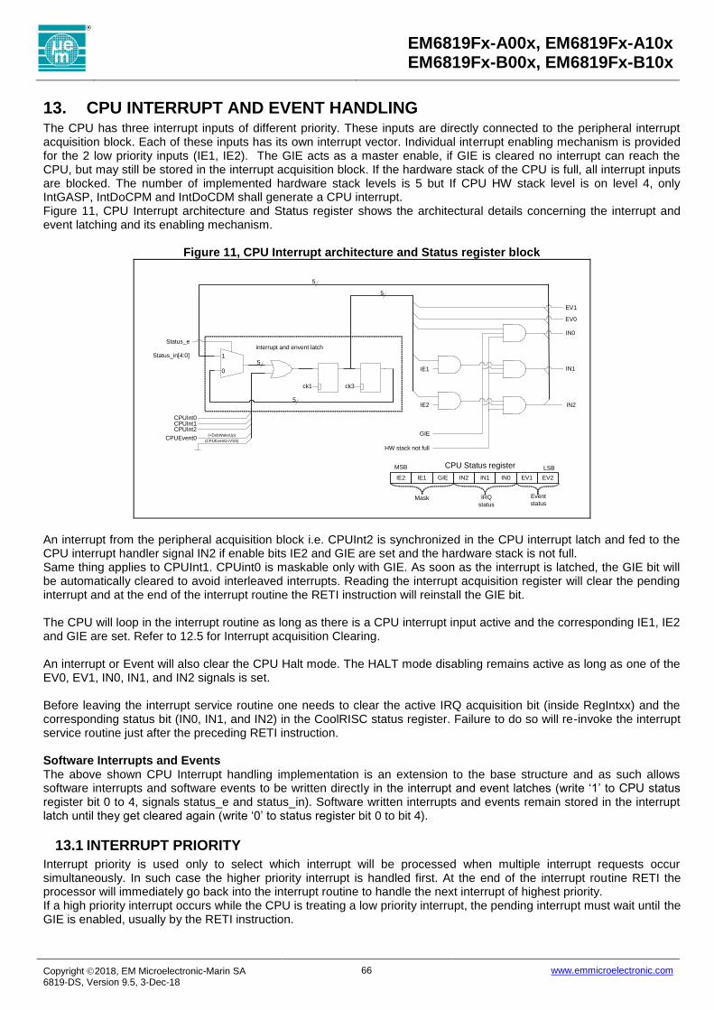
EM6819Fx-A00x, EM6819Fx-A10x EM6819Fx-B00x, EM6819Fx-B10x
Copyright 2018, EM Microelectronic-Marin SA 6819-DS, Version 9.5, 3-Dec-18
66 www.emmicroelectronic.com
13. CPU INTERRUPT AND EVENT HANDLING The CPU has three interrupt inputs of different priority. These inputs are directly connected to the peripheral interrupt acquisition block. Each of these inputs has its own interrupt vector. Individual interrupt enabling mechanism is provided for the 2 low priority inputs (IE1, IE2). The GIE acts as a master enable, if GIE is cleared no interrupt can reach the CPU, but may still be stored in the interrupt acquisition block. If the hardware stack of the CPU is full, all interrupt inputs are blocked. The number of implemented hardware stack levels is 5 but If CPU HW stack level is on level 4, only IntGASP, IntDoCPM and IntDoCDM shall generate a CPU interrupt. Figure 11, CPU Interrupt architecture and Status register shows the architectural details concerning the interrupt and event latching and its enabling mechanism.
Figure 11, CPU Interrupt architecture and Status register block
HW stack not full
GIE
IE2
IE1
1
0
ck3ck1
5
5
CPUInt0CPUInt1CPUInt2
CPUEvent0(CPUEvent1=VSS)
(=DebWakeUp)
Status_e
Status_in[4:0]
interrupt and envent latch
5
5
IN2
IN1
IN0
EV0
EV1
CPU Status register
IE2 IE1 GIE IN2 IN1 IN0 EV1 EV2
MSB LSB
Mask IRQ
status
Event
status
An interrupt from the peripheral acquisition block i.e. CPUInt2 is synchronized in the CPU interrupt latch and fed to the CPU interrupt handler signal IN2 if enable bits IE2 and GIE are set and the hardware stack is not full. Same thing applies to CPUInt1. CPUint0 is maskable only with GIE. As soon as the interrupt is latched, the GIE bit will be automatically cleared to avoid interleaved interrupts. Reading the interrupt acquisition register will clear the pending interrupt and at the end of the interrupt routine the RETI instruction will reinstall the GIE bit. The CPU will loop in the interrupt routine as long as there is a CPU interrupt input active and the corresponding IE1, IE2 and GIE are set. Refer to 12.5 for Interrupt acquisition Clearing. An interrupt or Event will also clear the CPU Halt mode. The HALT mode disabling remains active as long as one of the EV0, EV1, IN0, IN1, and IN2 signals is set. Before leaving the interrupt service routine one needs to clear the active IRQ acquisition bit (inside RegIntxx) and the corresponding status bit (IN0, IN1, and IN2) in the CoolRISC status register. Failure to do so will re-invoke the interrupt service routine just after the preceding RETI instruction. Software Interrupts and Events The above shown CPU Interrupt handling implementation is an extension to the base structure and as such allows software interrupts and software events to be written directly in the interrupt and event latches (write ‘1’ to CPU status register bit 0 to 4, signals status_e and status_in). Software written interrupts and events remain stored in the interrupt latch until they get cleared again (write ‘0’ to status register bit 0 to bit 4).
13.1 INTERRUPT PRIORITY
Interrupt priority is used only to select which interrupt will be processed when multiple interrupt requests occur simultaneously. In such case the higher priority interrupt is handled first. At the end of the interrupt routine RETI the processor will immediately go back into the interrupt routine to handle the next interrupt of highest priority. If a high priority interrupt occurs while the CPU is treating a low priority interrupt, the pending interrupt must wait until the GIE is enabled, usually by the RETI instruction.

EM6819Fx-A00x, EM6819Fx-A10x EM6819Fx-B00x, EM6819Fx-B10x
Copyright 2018, EM Microelectronic-Marin SA 6819-DS, Version 9.5, 3-Dec-18
67 www.emmicroelectronic.com
13.2 CPU STATUS REGISTER
The status register, used to control the interrupts and events, is an internal register to the CoolRISC CPU. It therefore does not figure in the peripheral memory mapping. All CPU enable bits for the interrupts and the current status of the events and the interrupts are part of this register.
Table 5. CPU status register description
Bit Name Reset Reset by R/W Description
7 IE2 0 ResSys R/W Level 2 Interrupt enable
‘1’ = enabled, ‘0’ = disabled
6 IE1 0 ResSys R/W Level 1 Interrupt enable
‘1’ = enabled, ‘0’ = disabled
5 GIE 0 ResSys R/W* General interrupt enable
‘1’ = enabled, ‘0’ = disabled
4 IN2 0 ResSys R/W Interrupt request level 2 flag, shows CPUInt2
‘1’ = IRQ pending, ‘0’ = no IRQ
The IRQ may only take place if IN2, IE2, and GIE are set
3 IN1 0 ResSys R/W Interrupt request level 1 flag, shows CPUInt1
‘1’ = IRQ pending, ‘0’ = no IRQ
The IRQ may only take place if IN1, IE1, and GIE are set
2 IN0 0 ResSys R/W Interrupt request level 0 flag, shows CPUInt1
‘1’ = IRQ pending, ‘0’ = no IRQ
The IRQ may only take place if IN0 and GIE are set
1 EV1 0 ResSys R/W Event request 1
0 EV0 0 ResSys R/W Event request 0
*Clear General Interrupt Enable bit GIE. Special care must be taken clearing the GIE bit. If an interrupt arrives during the clear operation the software may still branch into the interrupt routine and will set the GIE bit by the interrupt routine ending RETI instruction. This behavior may prevent from creating 'interrupt protected' areas within your code. A suitable workaround is to check if the GIE clearing took effect (Instruction) TSTB before executing the protected section.
13.3 CPU STATUS REGISTER PIPELINE EXCEPTION
Another consequence of the above interrupt implementation is that several instruction sequences work in a different way than expected. These instructions are mostly related to interrupt and event signals. For ‘normal’ instructions the pipeline is completely transparent. If an interrupt is set by software (i.e. write into the status register with a MOVE stat) the pipeline causes the next instruction to be executed before the processor jumps to the interrupt subroutine. This allows one to supply a parameter to a ‘trap’ as in Code shown below.
SETB stat, #4 ; trap MOVE a #parameter ;
If an event bit is set by software (i.e. write into the CPU status register with a MOVE stat) and if a JEV (jump on event) instruction immediately follows the move, the jump on event will act as if the move has not been executed, since the write into the CPU status register will occur only once the JEV has been executed. The move takes 3 cycles to be executed and the JEV only one.

EM6819Fx-A00x, EM6819Fx-A10x EM6819Fx-B00x, EM6819Fx-B10x
Copyright 2018, EM Microelectronic-Marin SA 6819-DS, Version 9.5, 3-Dec-18
68 www.emmicroelectronic.com
13.4 PROCESSOR VECTOR TABLE
Address 1, 2 and 3 of the program memory are reserved for interrupt subroutine calls. Generally the first four addresses of the program memory are reserved for the processor vector table. The address 0 of the program memory contains the jump to the start-up routine Table 6. Processor vector table
Address Accessed by Description Priority
0 ResSys Any reset, start-up address Maximal, above interrupts
1 IN1 Interrupt level 1 medium
2 IN2 Interrupt level 2 low
3 IN3 Interrupt level 0 high
13.5 CONTEXT SAVING
Since an interrupt may occur any time during normal program execution, there is no way to know which processor registers are used by the user program. For this reason, all resources modified in the interrupt service routine have to be saved upon entering and restored when leaving the service routine. The flags(C, V) and the accumulator (A) must always be saved, since most instructions will modify them. Other registers need only to be saved when they are modified in the interrupt service routine. There is a particular way to follow when saving resources. The accumulator should be saved first, followed by the flags and then the other registers

EM6819Fx-A00x, EM6819Fx-A10x EM6819Fx-B00x, EM6819Fx-B10x
Copyright 2018, EM Microelectronic-Marin SA 6819-DS, Version 9.5, 3-Dec-18
69 www.emmicroelectronic.com
14. PORT A The port A is general purpose 8-bit input output port. Each of the 8 Port A terminals can be configured to receive either Analog or digital Input or drive out analog or digital data.
14.1 PORT A TERMINAL MAPPING
Several digital and analog functions are mapped on the port A terminals. Please refer also to the concerned chapters. Table 14.1-1 Port A terminal mapping
Name IRQ ADC
Reset &
WkUp VREF VLD OPAMP SPI CLOCK
Timer
clock
Timer
start
PWM
FrqOut
output
strength
PA0 PAIRQ0 ADC0 Rst_Wkup0 t1ck0_in start1_in sig
PA1 PAIRQ1 ADC2 Rst_Wkup1 VLD OPA_Out t2ck0_in start2_in sig
PA2 PAIRQ2 ADC4 Rst_Wkup2 Vref_ADC VLD OPA_INMSIN
SOUTt3ck0_in start4_in sig
PA3 PAIRQ3 ADC6 Rst_Wkup3 OPA_INP t4ck0_in start5_in sig HD
PA4 PAIRQ4 Rst_Wkup4 SIN XIN sig
PA5 PAIRQ5 Rst_Wkup5 sig HD
PA6 PAIRQ6 Rst_Wkup6 Vref_out VLD SCLK sig HD
PA7 PAIRQ7 Rst_Wkup7 VLD SOUT sig HD
Note: on all bit of port A debouncers are enable by default after reset.
14.2 PORT A IO OPERATION
All IO modes are individually selectable for each port A terminal. Refer to table below. Table 14.2-1 Port A IO selections
Modes
PA
OE
[n
]
PA
[n] O
utp
ut
data
PA
OD
[n]
PA
PU
[n]
PA
PD
[n]
PA
Inp
E[n
]
PA
[n]
Term
inal
Notes
Analog signal connection (in out) 0 X X 0 0 0 High-Z Digital input is blocked, Analog functions can be connected CPU reads ‘0’
Analog signal connection (in out) with weak load to VDD or VSS
0 X X 1 X 0 RLoad to VDD
0 X X 0 1 0 RLoad to VSS
Input mode 0 X X 0 0 1 High-Z Digital input, no-pull, needs external driver
Input mode with pull-up 0 X X 1 X 1 Weak Hi Digital input with pullup
Input mode with pull-down 0 X X 0 1 1 Weak Lo Digital input with pulldown
Output, CMOS high level drive 1 1 0 X X X 1 Pull resistors disabled
Output, CMOS low level drive 1 0 0 X X X 0 Pull resistors disabled
Output, open drain, high-Z 1 1 1 0 X X High-Z Pull-down disabled, Usually ext Resistor pull-up
Output, open drain with pull-up 1 1 1 1 X X Weak Hi Pull-up active
Output, open drain low level drive 1 0 1 X X X 0 Pull-up disabled

EM6819Fx-A00x, EM6819Fx-A10x EM6819Fx-B00x, EM6819Fx-B10x
Copyright 2018, EM Microelectronic-Marin SA 6819-DS, Version 9.5, 3-Dec-18
70 www.emmicroelectronic.com
Figure 12; Port A IO configuration
PAPD[n]
PA[n] output data
PAInpEn[n]
PAOD[n]
PAPU[n]
PA[n]
Read
RegPADin
Data-bus
ck
Debouncer-clocked mode
-transparent
mode
PA input data to:
- timer
- SPI
- PA reset
- PA-IRQ
PA[n]DebSel1,0
PADOut[n]
clocks
clocks
clocks
PA IO configuration architecture
70 KOhm
70 KOhm
PADIn[n]
ANALOG IO
PA[n]OutSel1,0
PA wake-up
PADeb[n]
For maximum flexibility all Port A configuration bits are are fully user configurable.
The pull resistors are only active if the pad driver is not driving the pad terminal, and pullup or pulldown resistors are enabled. Pullup has priority over pulldown.
The CPU read of the port A terminal logic value (PA[n]) in register RegPADIn is depending of the PAInpEn blocking bit. As such one reads ‘0’ if PAInpEn=’0’ (Input blocked) and the terminal logic value if PAInpEn=’1’.
At power-up, the PA[n] terminals are tristate with pullup and pulldown resistors disconnected and the input is disabled. As such all PA terminal can float without the penalty of additional power consumption.
All PA input signal sources for Timer, SPI, PA-Reset, PA-IRQ are coming from the debouncer output PADeb[n]. Note: Make sure to setup the terminal correctly before using it as either digital IO or as an analog connection.

EM6819Fx-A00x, EM6819Fx-A10x EM6819Fx-B00x, EM6819Fx-B10x
Copyright 2018, EM Microelectronic-Marin SA 6819-DS, Version 9.5, 3-Dec-18
71 www.emmicroelectronic.com
14.3 OUTPUT SIGNALS ON PORT A
Different internal clock frequencies and PWM signals can be outout on all port A terminals. (PA[n] Output data)
The selection is done with the registers PA[n]OutSel1,0 . All clock outputs (PR1_x, PR2_x) have a 50% duty cycle. The Clock outputs CK_x have a duty cycle corresponding to the duty cycle of their clock source.
By default the register data PADOut[n] value is seleted as data output.
Data is only output if the corresponding PAOutEn[n] bit is high. Table 14.3-1 Port AOutput signal selection
PA0OutSel1 PA0OutSel0 PA0 Output Data remarks
0 0 PADOut[0]
0 1 PWM3_N
1 0 PWM2_N1 1 PWM4_N
PA1OutSel1 PA1OutSel0 PA1 Output Data remarks
0 0 PADOut[1]
0 1 Pr1Ck11 2kHz if CK_PR1=32kHz
1 0 PWM11 1 PWM2_N
PA2OutSel1 PA2OutSel0 PA2 Output Data remarks
0 0 PADOut[2]
0 1 SOUT
1 0 PWM11 1 Ck_Hi
PA3OutSel1 PA3OutSel0 PA3 Output Data remarks
0 0 PADOut[3]
0 1 Ck_Lo
1 0 Pr1Ck11 2kHz if CK_PR1=32kHz1 1 Pr1Ck10 1kHz if CK_PR1=32kHz
PA4OutSel1 PA4OutSel0 PA4 Output Data remarks
0 0 PA-DOut[4]
0 1 Ck_Hi_N
1 0 Pr2Ck6_N 125kHz if CK_PR2=2MHz1 1 Pr2Ck4_N 31kHz if CK_PR2=2MHz
PA5OutSel1 PA5OutSel0 PA5 Output Data remarks
0 0 PADOut[5]
0 1 PWM3
1 0 PWM21 1 PWM4
PA6OutSel1 PA6OutSel0 PA6 Output Data remarks
0 0 PADOut[6]
0 1 SCLK
1 0 PWM1_N1 1 CK_8K
PA7OutSel1 PA7OutSel0 PA7 Output Data remarks
0 0 PADOut[7]
0 1 SOUT
1 0 Pr1Ck11_N 2kHz if CK_PR1=32kHz1 1 Pr1Ck10_N 1kHz if CK_PR1=32kHz
Wheras:
PWM3 = PWM output of timer 3 (refer to timer section)
PWM3_N = inverse PWM output of timer 3
Ck_Lo = Low frequency base clock (refer to clock selection)
CK_Lo_N = inverse Low frequency base clock
Pr1Ck11 = Prescaler 1, ck11 output (refer to prescaler)

EM6819Fx-A00x, EM6819Fx-A10x EM6819Fx-B00x, EM6819Fx-B10x
Copyright 2018, EM Microelectronic-Marin SA 6819-DS, Version 9.5, 3-Dec-18
72 www.emmicroelectronic.com
14.4 PORT A DEBOUNCER
Each Port A input has its own debouncer with an independent clock selection. The debouncer is either transparent or clocked. The debouncer output signal is called PADeb[n]
Transparent Mode: The input is immediately available on its output.
Clocked mode: The debouncer copies is input state to its output only if during 2 consecutive debouncer clock events the debouncer input signal remains stable. The debouncer is reset on POR, in Power-Down mode, by a watchdog reset and a bus error reset.
Table 14.4-1 Port A Debouncer Mode and Clock selection
PA[n]DebSel1 PA[n]DebSel0 Clock Mode remarks
0 0 Pr1Ck7 Clocked Clocked; 128 Hz if ck_pr1=32kHz
0 1 Pr1Ck15 Clocked Clocked; Pr1 input clock
1 0 Pr2Ck10 Clocked Clocked; Pr2 input clock1 1 no clock Transparent Output = Input
14.5 PORT A INTERRUPT GENERATION
Each port A input may be used as Interrupt source with individual masking possibilities.
14.5.1 PA IRQ IN ACTIVE AND STANDBY MODE
The clocked PortA interrupt is generated in the Active and Standby modes only.
A positive or negative edge of the debouncer output signal PADeb[n] shall generate the IntPA[n]. The edge selection is done by the register bit PAIntEdg[n] (‘1’ means a positive edge and it’s the default state).
The IntPA signal is the input to the interrupt controller.(refer to the interrupt controller for Irq masking and handling).
All interrupt settings are independent for each PA input.
14.5.2 PA IRQ IN SLEEP MODE
In Sleep mode, any edge (positive or negative) of the PA[n] input while PAInpEn[n]=1 will generate an IntPA request.
The IntPA signal is the input to the interrupt controller.(refer to the interrupt controller for Irq masking and handling).
All interrupt settings are independent for each PA input.
14.6 PORT A RESET FUNCTION
Each port A input can be used to generate a system reset (ResSys in Reset controller).
The Port A reset signal ResPA is a logical OR function of all PA input reset sources after masking.
The input signals for the port A reset function are coming from the Port A debouncer output PADeb[n] and can be masked individually with RegEnResPA[n]=’0’ . Default: all inputs are masked and no PA reset is generated.
The ResPA is the output of the port A reset function and the input signal to the reset controller.
14.7 PORT A WAKE-UP FUNCTION
Each port A input can be used to wake-up the circuit from Power-Down mode.
In Power-Down mode, any state change of a selected PA[n] input while its PAInpEn[n]=1 will cancel wake-up and resume to active mode. A PA[n] input is only selected for wake-up if its EnWkUp[n] bit is at high level.

EM6819Fx-A00x, EM6819Fx-A10x EM6819Fx-B00x, EM6819Fx-B10x
Copyright 2018, EM Microelectronic-Marin SA 6819-DS, Version 9.5, 3-Dec-18
73 www.emmicroelectronic.com
14.8 PORT A REGISTERS
0x000A RegPADIn Port-A Data Input
Bits Name Type ResVal ResSrc Description
7:0 PADIn RO 0x00 ResSys Port-A Data Input
0x000B RegPADOut Port-A Data Output
Bits Name Type ResVal ResSrc Description
7:0 PADOut RW_Res 0x00 ResSys Port-A Data Output
0x000C RegPAInpE Port-A Input Enable
Bits Name Type ResVal ResSrc Description
7:0 PAInpE RW_Res 0x00 ResAna Port-A Input Enable
0x000D RegPAOE Port-A Output Enable
Bits Name Type ResVal ResSrc Description
7:0 PAOE RW_Res 0x00 ResAna Port-A Output Enable
0x000E RegPAPU Port-A Pull Up
Bits Name Type ResVal ResSrc Description
7:0 PAPU RW 0x00 PorLog Port-A Pull Up
0x000F RegPAPD Port-A Pull Down
Bits Name Type ResVal ResSrc Description
7:0 PAPD RW 0x00 PorLog Port-A Pull Down
0x0010 RegPAOD Port-A Open Drain
Bits Name Type ResVal ResSrc Description
7:0 PAOD RW 0x00 ResSys Port-A Open Drain
0x0015 RegPAIntEdg Port-A Interrupt Edge Selection: 1-Rising, 0-Falling
Bits Name Type ResVal ResSrc Description
7:0 PAIntEdg RW 0xFF ResSys Port-A Interrupt Edge Selection: 1-Rising, 0-Falling
0x0011 RegPAOutCfg0 Port-A Output Configuration/Selection - 0
Bits Name Type ResVal ResSrc Description
7:6 PA3OutSel RW ‘00’ ResSys Port-A3 Output Configuration/Selection
5:4 PA2OutSel RW ‘00’ ResSys Port-A2 Output Configuration/Selection
3:2 PA1OutSel RW ‘00’ ResSys Port-A1 Output Configuration/Selection
1:0 PA0OutSel RW ‘00’ ResSys Port-A0 Output Configuration/Selection
0x0012 RegPAOutCfg1 Port-A Output Configuration/Selection - 1
Bits Name Type ResVal ResSrc Description
7:6 PA7OutSel RW ‘00’ ResSys Port-A7 Output Configuration/Selection
5:4 PA6OutSel RW ‘00’ ResSys Port-A6 Output Configuration/Selection
3:2 PA5OutSel RW ‘00’ ResSys Port-A5 Output Configuration/Selection
1:0 PA4OutSel RW ‘00’ ResSys Port-A4 Output Configuration/Selection
0x0013 RegPADebCfg1 Port-A Deboucer Configuration - 1
Bits Name Type ResVal ResSrc Description
7:6 PA3DebSel RW ‘00’ ResAna PA(3) Deboucer clock Selection/Enable
5:4 PA2DebSel RW ‘00’ ResAna PA(2) Deboucer clock Selection/Enable
3:2 PA1DebSel RW ‘00’ ResAna PA(1) Deboucer clock Selection/Enable
1:0 PA0DebSel RW ‘00’ ResAna PA(0) Deboucer clock Selection/Enable

EM6819Fx-A00x, EM6819Fx-A10x EM6819Fx-B00x, EM6819Fx-B10x
Copyright 2018, EM Microelectronic-Marin SA 6819-DS, Version 9.5, 3-Dec-18
74 www.emmicroelectronic.com
0x0014 RegPADebCfg2 Port-A Deboucer Configuration - 2
Bits Name Type ResVal ResSrc Description
7:6 PA7DebSel RW ‘00’ ResAna PA(7) Deboucer clock Selection/Enable
5:4 PA6DebSel RW ‘00’ ResAna PA(6) Deboucer clock Selection/Enable
3:2 PA5DebSel RW ‘00’ ResAna PA(5) Deboucer clock Selection/Enable
1:0 PA4DebSel RW ‘00’ ResAna PA(4) Deboucer clock Selection/Enable
0x0001 RegEnResPA Enable Reset by PortA bits
Bits Name Type ResVal ResSrc Description
7:0 EnResPA RW 0x00 ResAna Enable Reset by PortA bits
0x0002 RegEnWkUpPA Enable of Wake Up from Power-Down by PortA
Bits Name Type ResVal ResSrc Description
7:0 EnWkUpPA RW 0x00 ResSys Enable of Wake Up from Power-Down by PA bits

EM6819Fx-A00x, EM6819Fx-A10x EM6819Fx-B00x, EM6819Fx-B10x
Copyright 2018, EM Microelectronic-Marin SA 6819-DS, Version 9.5, 3-Dec-18
75 www.emmicroelectronic.com
15. PORT B The port B is general purpose 8-bit input output port. Each of the 8 Port B terminals can be configured to receive either Analog or digital Input or drive out analog or digital data. The port B, PB7 and PB6 terminals, are special inputs for device programming and debugging. These 2 ports will have special configurations as soon as TM terminal is high to allow Gasp (ISP, DoC) accesses.
15.1 PORT B TERMINAL MAPPING
Several digital and analog functions are mapped on the port B terminals. Please refer also to the concerned chapters. Table 15.1-1 Port B terminal mapping
Name IRQ ADCReset &
WkUpVREF VLD OPAMP SPI GASP CLOCK
Timer
clock
Timer
start
PWM
FrqOut
output
strength
PB0 SIN sig HD
PB1 sig HD
PB2 SCLK sig HD
PB3 sig HD
PB4 SOUT sig HD
PB5 sig HD
PB6 GASP-SCK sig HD
PB7 GASP-SIO sig HD
15.2 PORT B IO OPERATION
All IO modes are individually selectable for each port B terminal. Refer to table below. Table 15.2-1 Port B IO selections
Modes
PB
OE
[n
]
PB
[n] O
utp
ut
data
PB
OD
[n]
PB
PU
[n]
PB
PD
[n]
PB
Inp
E[n
]
PB
[n]
Term
inal
Notes
Analog signal connection (in out) 0 X X 0 0 0 High-Z Digital input is blocked, Analog functions can be connected CPU reads ‘0’
Analog signal connection (in out) with weak load to VDD or VSS
0 X X 1 X 0 RLoad to VDD
0 X X 0 1 0 RLoad to VSS
Input mode 0 X X 0 0 1 High-Z Digital input, no-pull, needs external driver
Input mode with pull-up 0 X X 1 X 1 Weak Hi Digital input with pullup
Input mode with pull-down 0 X X 0 1 1 Weak Lo Digital input with pulldown
Output, CMOS high level drive 1 1 0 X X X 1 Pull resistors disabled
Output, CMOS low level drive 1 0 0 X X X 0 Pull resistors disabled
Output, open drain, high-Z 1 1 1 0 X X High-Z Pull-down disabled, Usually ext Resistor pull-up
Output, open drain with pull-up 1 1 1 1 X X Weak Hi Pull-up active
Output, open drain drive low 1 0 1 X X X 0 Pull-up disabled
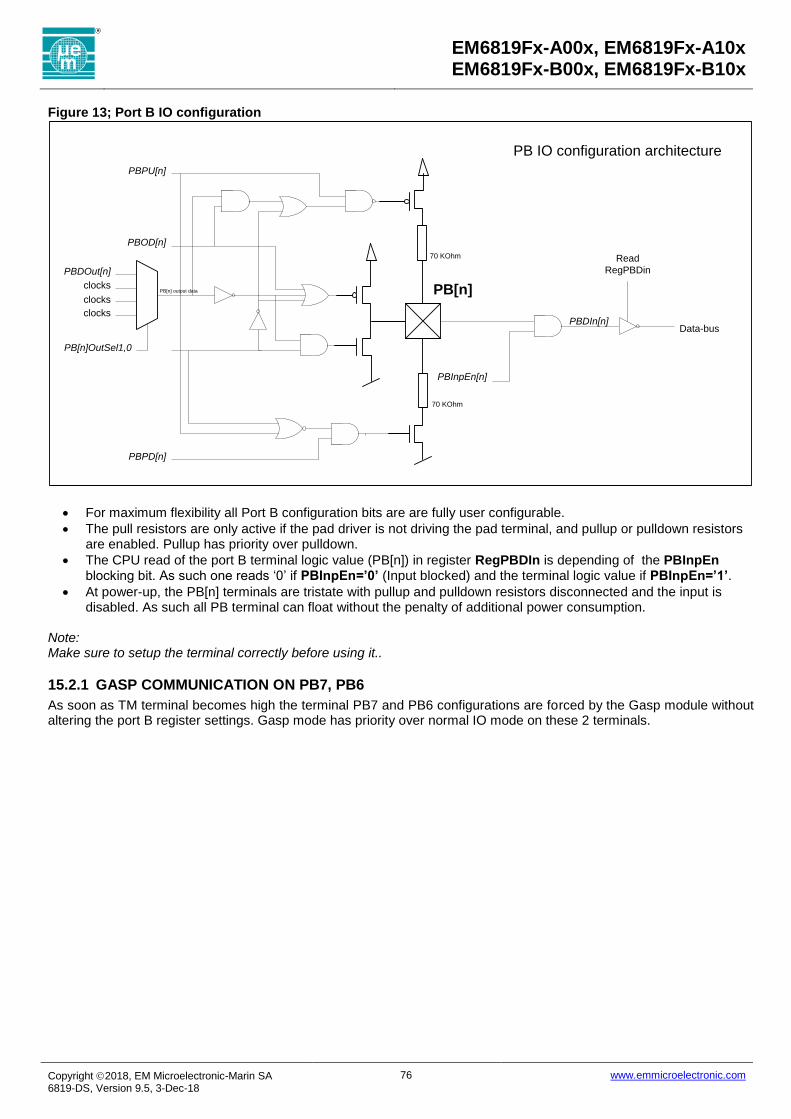
EM6819Fx-A00x, EM6819Fx-A10x EM6819Fx-B00x, EM6819Fx-B10x
Copyright 2018, EM Microelectronic-Marin SA 6819-DS, Version 9.5, 3-Dec-18
76 www.emmicroelectronic.com
Figure 13; Port B IO configuration
PBPD[n]
PB[n] output data
PBInpEn[n]
PBOD[n]
PBPU[n]
PB[n]
Read
RegPBDin
Data-bus
PBDOut[n]
clocks
clocks
clocks
PB IO configuration architecture
70 KOhm
70 KOhm
PBDIn[n]
PB[n]OutSel1,0
For maximum flexibility all Port B configuration bits are are fully user configurable.
The pull resistors are only active if the pad driver is not driving the pad terminal, and pullup or pulldown resistors are enabled. Pullup has priority over pulldown.
The CPU read of the port B terminal logic value (PB[n]) in register RegPBDIn is depending of the PBInpEn blocking bit. As such one reads ‘0’ if PBInpEn=’0’ (Input blocked) and the terminal logic value if PBInpEn=’1’.
At power-up, the PB[n] terminals are tristate with pullup and pulldown resistors disconnected and the input is disabled. As such all PB terminal can float without the penalty of additional power consumption.
Note: Make sure to setup the terminal correctly before using it..
15.2.1 GASP COMMUNICATION ON PB7, PB6
As soon as TM terminal becomes high the terminal PB7 and PB6 configurations are forced by the Gasp module without altering the port B register settings. Gasp mode has priority over normal IO mode on these 2 terminals.

EM6819Fx-A00x, EM6819Fx-A10x EM6819Fx-B00x, EM6819Fx-B10x
Copyright 2018, EM Microelectronic-Marin SA 6819-DS, Version 9.5, 3-Dec-18
77 www.emmicroelectronic.com
15.3 OUTPUT SIGNALS ON PORT B
Different internal clock frequencies and PWM signals can be outout on all port B terminals. (PB[n] Output data)
The selection is done with the registers PB[n]OutSel1,0 . All clock outputs (Pr1ckx, Pr2ckx) have a 50% duty cycle. The Clock outputs CK_x have a duty cycle corresponding to the duty cycle of their clock source.
By default the register data PBDOut[n] value is seleted as data output.
Data is only output if the corresponding PBOutEn[n] bit is high. Table 15.3-1 Port B Output signal selection
PB0OutSel1 PB0OutSel0 PB0 Output Data remarks
0 0 PBDOUT[0]
0 1 PWM3
1 0 PWM21 1 PWM4
PB1OutSel1 PB1OutSel0 PB1 Output Data remarks
0 0 PBDOUT[1]
0 1 PWM3_N
1 0 PWM2_N1 1 PWM4_N
PB2OutSel1 PB2OutSel0 PB2 Output Data remarks
0 0 PBDOUT[2]
0 1 SCLK
1 0 PWM11 1 PWM3
PB3OutSel1 PB3OutSel0 PB3 Output Data remarks
0 0 PBDOUT[3]
0 1 CK_Hi
1 0 PWM1_N1 1 PWM3_N
PB4OutSel1 PB4OutSel0 PB4 Output Data remarks
0 0 PBDOUT[4]
0 1 SOUT
1 0 PWM11 1 PWM3
PB5OutSel1 PB5OutSel0 PB5 Output Data remarks
0 0 PBDOUT[5]
0 1 PWM3
1 0 PWM21 1 PWM4
PB6OutSel1 PB6OutSel0 PB6 Output Data remarks
0 0 PBDOUT[6]
0 1 PWM1_N
1 0 PWM3_N1 1 Pr1Ck11 2kHz if CK_PR1=32kHz
PB7-OutSel1 PB7-OutSel0 PB7 Output Data remarks
0 0 PBDOUT[7]
0 1 PWM1
1 0 PWM31 1 Pr1Ck10 1kHz if CK_PR1=32kHz
Wheras:
PWM3 = PWM output of timer 3 (refer to timer section)
PWM3_N = inverse PWM output of timer 3
Ck_Hi = High frequency base clock (refer to clock selection)
Pr1Ck10 = Prescaler 1, ck10 output (refer to prescaler)

EM6819Fx-A00x, EM6819Fx-A10x EM6819Fx-B00x, EM6819Fx-B10x
Copyright 2018, EM Microelectronic-Marin SA 6819-DS, Version 9.5, 3-Dec-18
78 www.emmicroelectronic.com
15.4 PORT B REGISTERS
0x0016 RegPBDin Port-B Data Input
Bits Name Type ResVal ResSrc Description
7:0 PBDIn RO 0x00 ResSys Port-B Data Input
0x0017 RegPBDOut Port-B Data Output
Bits Name Type ResVal ResSrc Description
7:0 PBDOut RW_Res 0x00 ResSys Port-B Data Output
0x0018 RegPBInpE Port-B Input Enable
Bits Name Type ResVal ResSrc Description
7:0 PBInpE RW_Res 0x00 ResSys Port-B Input Enable
0x0019 RegPBOE Port-B Output Enable
Bits Name Type ResVal ResSrc Description
7:0 PBOE RW_Res 0x00 ResSys Port-B Output Enable
0x001A RegPBPU Port-B Pull Up
Bits Name Type ResVal ResSrc Description
7:0 PBPU RW_Res 0x00 PorLog Port-B Pull Up
0x001B RegPBPD Port-B Pull Down
Bits Name Type ResVal ResSrc Description
7:0 PBPD RW_Res 0x00 PorLog Port-B Pull Down
0x001C RegPBOD Port-B Open Drain
Bits Name Type ResVal ResSrc Description
7:0 PBOD RW_Res 0x00 ResSys Port-B Open Drain
0x001D RegPBOutCfg0 Port-B Output Configuration/Selection - 0
Bits Name Type ResVal ResSrc Description
7:6 PB3OutSel RW '00' ResSys Port-B3 Output Configuration/Selection
5:4 PB2OutSel RW '00' ResSys Port-B2 Output Configuration/Selection
3:2 PB1OutSel RW '00' ResSys Port-B1 Output Configuration/Selection
1:0 PB0OutSel RW '00' ResSys Port-B0 Output Configuration/Selection
0x001E RegPBOutCfg1 Port-B Output Configuration/Selection - 1
Bits Name Type ResVal ResSrc Description
7:6 PB7OutSel RW '00' ResSys Port-B7 Output Configuration/Selection
5:4 PB6OutSel RW '00' ResSys Port-B6 Output Configuration/Selection
3:2 PB5OutSel RW '00' ResSys Port-B5 Output Configuration/Selection
1:0 PB4OutSel RW '00' ResSys Port-B4 Output Configuration/Selection

EM6819Fx-A00x, EM6819Fx-A10x EM6819Fx-B00x, EM6819Fx-B10x
Copyright 2018, EM Microelectronic-Marin SA 6819-DS, Version 9.5, 3-Dec-18
79 www.emmicroelectronic.com
16. PORT C The port C is general purpose 8-bit input output port. Each of the 8 Port C terminals can be configured to receive either Analog or digital Input or drive out analog or digital data.
16.1 PORT C TERMINAL MAPPING
Several digital and analog functions are mapped on the port C terminals. Please refer also to the concerned chapters. Table 16.1-1 Port C terminal mapping
Name IRQ ADCReset &
WkUpVREF VLD OPAMP SPI CLOCK
Timer
clock
Timer
start
PWM
FrqOut
output
strength
PC0 PCIRQ0 ADC1 sig
PC1 PCIRQ1 ADC3 VLD OPA_Out t2ck1_in start3_in sig
PC2 PAIRQ2 ADC5 OPA_INM SOUT sig
PC3 PCIRQ3 ADC7 OPA_INP t4ck1_in start6_in sig HD
PC4 PCIRQ4XOUT
ExtCksig
PC5 PCIRQ5 VLD sig HD
PC6 PCIRQ6 VLD SCLK t1ck1_in start7_in sig HD
PC7 PCIRQ7 t3ck1_in sig
16.2 PORT C IO OPERATION
All IO modes are individually selectable for each port C terminal. Refer to table below. Table 16.2-1 Port C IO selections
Modes
PC
OE
[n
]
PC
[n]
Outp
ut d
ata
PC
OD
[n]
PC
PU
[n]
PC
PD
[n]
PC
Inp
E[n
]
PC
[n]
Term
inal
Notes
Analog signal connection (in out) 0 X X 0 0 0 High-Z Digital input is blocked, Analog functions can be connected CPU reads ‘0’
Analog signal connection (in out) with weak load to VDD or VSS
0 X X 1 X 0 RLoad to VDD
0 X X 0 1 0 RLoad to VSS
Input mode 0 X X 0 0 1 High-Z Digital input, no-pull, needs external driver
Input mode with pull-up 0 X X 1 X 1 Weak Hi Digital input with pullup
Input mode with pull-down 0 X X 0 1 1 Weak Lo Digital input with pulldown
Output, CMOS high level drive 1 1 0 X X X 1 Pull resistors disabled
Output, CMOS low level drive 1 0 0 X X X 0 Pull resistors disabled
Output, open drain, high-Z 1 1 1 0 X X High-Z Pull-down disabled, Usually ext Resistor pull-up
Output, open drain with pull-up 1 1 1 1 X X Weak Hi Pull-up active
Output, open drain drive low 1 0 1 X X X 0 Pull-up disabled
Note: on all bit of port C debouncers are enable by default after reset,

EM6819Fx-A00x, EM6819Fx-A10x EM6819Fx-B00x, EM6819Fx-B10x
Copyright 2018, EM Microelectronic-Marin SA 6819-DS, Version 9.5, 3-Dec-18
80 www.emmicroelectronic.com
Figure 14; Port C IO configuration
PCPD[n]
PA[n] output data
PCInpEn[n]
PCOD[n]
PCPU[n]
PC[n]
Read
RegPADin
Data-bus
ck
Debouncer-clocked mode
-transparent
mode
PC input data to:
- timer
- SPI
- PC-IRQ
PC[n]DebSel1,0
PCDOut[n]
clocks
clocks
clocks
PC IO configuration architecture
70 KOhm
70 KOhm
PADIn[n]
ANALOG IO
PC[n]OutSel1,0
PCDeb[n]
For maximum flexibility all Port C configuration bits are are fully user configurable.
The pull resistors are only active if the pad driver is not driving the pad terminal, and pullup or pulldown resistors are enabled. Pullup has priority over pulldown.
The CPU read of the port C terminal logic value (PC[n]) in register RegPCDIn is depending of the PCInpEn blocking bit. As such one reads ‘0’ if PCInpEn=’0’ (Input blocked) and the terminal logic value if PCInpEn=’1’.
At power-up, the PC[n] terminals are tristate with pullup and pulldown resistors disconnected and the input is disabled. As such all PC terminal can float without the penalty of additional power consumption.
All PC input signal sources for Timer, SPI, PC-IRQ are coming from the debouncer output PCDeb[n]. Note: Make sure to setup the terminal correctly before using it as either digital IO or as an analog connection.

EM6819Fx-A00x, EM6819Fx-A10x EM6819Fx-B00x, EM6819Fx-B10x
Copyright 2018, EM Microelectronic-Marin SA 6819-DS, Version 9.5, 3-Dec-18
81 www.emmicroelectronic.com
16.3 OUTPUT SIGNALS ON PORT C
Different internal clock frequencies and PWM signals can be outout on all port C terminals. (PA[n] Output data)
The selection is done with the registers PC[n]OutSel1,0 . All clock outputs (Pr1ckx, Pr2ckx) have a 50% duty cycle. The Clock outputs CK_x have a duty cycle corresponding to the duty cycle of their clock source.
By default the register data PCDOut[n] value is seleted as data output.
Data is only output if the corresponding PCOutEn[n] bit is high. Table 16.3-1 Port C Output signal selection
PC0OutSel1 PC0OutSel0 PC0 Output Data remarks
0 0 PCDOUT[0]
0 1 Pr2Ck6 125kHz if CK_PR2=2MHz
1 0 Pr2Ck4 31kHz if CK_PR2=2MHz
1 1 Pr2Ck0 2kHz if CK_PR2=2MHz
PC1OutSel1 PC1OutSel0 PC1 Output Data remarks
0 0 PCDOUT[1]
0 1 PWM4_N
1 0 PWM1_N
1 1 PWM3_N
PC2OutSel1 PC2OutSel0 PC2 Output Data remarks
0 0 PCDOUT[2]
0 1 SOUT
1 0 PWM1_N
1 1 Ck_Lo
PC3OutSel1 PC3OutSel0 PC3 Output Data remarks
0 0 PCDOUT[3]
0 1 CK_LO_N
1 0 Pr1Ck11_N 2kHz if CK_PR1=32kHz
1 1 Pr1Ck10_N 1kHz if CK_PR1=32kHz
PC4OutSel1 PC4OutSel0 PC4 Output Data remarks
0 0 PCDOUT[4]
0 1 Ck_Hi
1 0 Pr2Ck6 125kHz if CK_PR2=2MHz
1 1 Pr2Ck4 31kHz if CK_PR2=2MHz
PC5OutSel1 PC5OutSel0 PC5 Output Data remarks
0 0 PCDOUT[5]
0 1 CK_8K
1 0 Pr2Ck6 125kHz if CK_PR2=2MHz
1 1 Pr2Ck4 31kHz if CK_PR2=2MHz
PC6OutSel1 PC6OutSel0 PC6 Output Data remarks
0 0 PCDOUT[6]
0 1 SCLK
1 0 PWM1_N
1 1 ck_lo
PC7OutSel1 PC7OutSel0 PC7 Output Data remarks
0 0 PCDOUT[7]
0 1 PWM1
1 0 PWM3_N1 1 Pr1Ck12 4kHz if CK_PR1=32kHz
Wheras:
PWM1 = PWM output of timer 1 (refer to timer section)
PWM1_N = inverse PWM output of timer 1
Ck_Hi = High frequency base clock (refer to clock selection)
Pr1Ck12 = Prescaler 1, ck12 output (refer to prescaler)

EM6819Fx-A00x, EM6819Fx-A10x EM6819Fx-B00x, EM6819Fx-B10x
Copyright 2018, EM Microelectronic-Marin SA 6819-DS, Version 9.5, 3-Dec-18
82 www.emmicroelectronic.com
16.4 PORT C DEBOUNCER
Each Port C input has its own debouncer with an independent clock selection. The debouncer is either transparent or clocked. The debouncer output signal is called PCDeb[n].
Transparent Mode: The input is immediately available on its output.
Clocked mode: The debouncer copies is input state to its output only if during 2 consecutive debouncer clock events the debouncer input signal remains stable. The debouncer is reset on POR, in Power-Down mode, by a watchdog reset and a bus error reset.
Table 16.4-1 Port C Debouncer Mode and Clock selection
PC[n]DebSel1 PC[n]DebSel0 Clock Mode remarks
0 0 Pr1Ck7 Clocked Clocked; 128 Hz if ck_pr1=32kHz
0 1 Pr1Ck15 Clocked Clocked; Pr1 input clock
1 0 Pr2Ck10 Clocked Clocked; Pr2 input clock1 1 no clock Transparent Output = Input
16.5 PORT C INTERRUPT GENERATION
Each port C input may be used as Interrupt source with individual masking possibilities.
16.5.1 PC IRQ IN ACTIVE AND STANDBY MODE
The clocked port C interrupt is generated in the Active and Standby modes only.
A positive or negative edge of the debouncer output signal PCDeb[n] shall generate the IntPC[n] interrupt request. The edge selection is done by the register bit PCIntEdg[n] (‘1’ means a positive edge and it’s the default state).
The IntPC signal is the input to the interrupt controller. (Refer to the interrupt controller for Irq masking and handling).
All interrupt settings are independent for each PC input.
16.5.2 PC IRQ IN SLEEP MODE
There is no port C interrupt possibility in Sleep mode. Port C interrupt input will automatically switch to the corresponding port A in Sleep mode. Refer also to the interrupt controller section 10

EM6819Fx-A00x, EM6819Fx-A10x EM6819Fx-B00x, EM6819Fx-B10x
Copyright 2018, EM Microelectronic-Marin SA 6819-DS, Version 9.5, 3-Dec-18
83 www.emmicroelectronic.com
16.6 PORT C REGISTERS
0x001F RegPCDin Port-C Data Input
Bits Name Type ResVal ResSrc Description
7:0 PCDIn RO 0x00 ResSys Port-C Data Input
0x0020 RegPCDOut Port-C Data Output
Bits Name Type ResVal ResSrc Description
7:0 PCDOut RW_Res 0x00 ResSys Port-C Data Output
0x0021 RegPCInpE Port-C Input Enable
Bits Name Type ResVal ResSrc Description
7:0 PCInpE RW_Res 0x00 ResSys Port-C Input Enable
0x0022 RegPCOE Port-C Output Enable
Bits Name Type ResVal ResSrc Description
7:0 PCOE RW_Res 0x00 ResSys Port-C Output Enable
0x0023 RegPCPU Port-C Pull Up
Bits Name Type ResVal ResSrc Description
7:0 PCPU RW_Res 0x00 PorLog Port-C Pull Up
0x0024 RegPCPD Port-C Pull Down
Bits Name Type ResVal ResSrc Description
7:0 PCPD RW_Res 0x00 PorLog Port-C Pull Down
0x0025 RegPCOD Port-C Open Drain
Bits Name Type ResVal ResSrc Description
7:0 PCOD RW_Res 0x00 ResSys Port-C Open Drain
0x002A RegPCIntEdg Port-C Interrupt Edge Selection: 1-Rising, 0-Falling
Bits Name Type ResVal ResSrc Description
7:0 PCIntEdg RW 0xFF ResSys Port-C Interrupt Edge Selection: 1-Rising, 0-Falling
0x0026 RegPCOutCfg0 Port-C Output Configuration/Selection - 0
Bits Name Type ResVal ResSrc Description
7:6 PC3OutSel RW '00' ResSys Port-C3 Output Configuration/Selection
5:4 PC2OutSel RW '00' ResSys Port-C2 Output Configuration/Selection
3:2 PC1OutSel RW '00' ResSys Port-C1 Output Configuration/Selection
1:0 PC0OutSel RW '00' ResSys Port-C0 Output Configuration/Selection
0x0027 RegPCOutCfg1 Port-C Output Configuration/Selection - 1
Bits Name Type ResVal ResSrc Description
7:6 PC7OutSel RW '00' ResSys Port-C7 Output Configuration/Selection
5:4 PC6OutSel RW '00' ResSys Port-C6 Output Configuration/Selection
3:2 PC5OutSel RW '00' ResSys Port-C5 Output Configuration/Selection
1:0 PC4OutSel RW '00' ResSys Port-C4 Output Configuration/Selection
0x0028 RegPCDebCfg1 Port-C Deboucer Configuration - 1
Bits Name Type ResVal ResSrc Description
7:6 PC3DebSel RW '00' ResSys PC(3) Deboucer clock Selection/Enable
5:4 PC2DebSel RW '00' ResSys PC(2) Deboucer clock Selection/Enable
3:2 PC1DebSel RW '00' ResSys PC(1) Deboucer clock Selection/Enable
1:0 PC0DebSel RW '00' ResSys PC(0) Deboucer clock Selection/Enable

EM6819Fx-A00x, EM6819Fx-A10x EM6819Fx-B00x, EM6819Fx-B10x
Copyright 2018, EM Microelectronic-Marin SA 6819-DS, Version 9.5, 3-Dec-18
84 www.emmicroelectronic.com
0x0029 RegPCDebCfg2 Port-C Deboucer Configuration - 2
Bits Name Type ResVal ResSrc Description
7:6 PC7DebSel RW '00' ResSys PC(7) Deboucer clock Selection/Enable
5:4 PC6DebSel RW '00' ResSys PC(6) Deboucer clock Selection/Enable
3:2 PC5DebSel RW '00' ResSys PC(5) Deboucer clock Selection/Enable
1:0 PC4DebSel RW '00' ResSys PC(4) Deboucer clock Selection/Enable

EM6819Fx-A00x, EM6819Fx-A10x EM6819Fx-B00x, EM6819Fx-B10x
Copyright 2018, EM Microelectronic-Marin SA 6819-DS, Version 9.5, 3-Dec-18
85 www.emmicroelectronic.com
17. TIMERS The circuit contains 4 independent 8-bit timers configurable as 2 16-bit timers.
Each of it can be individually configured with:
6 internal clock sources and 2 external clock sources from PA, PC terminals
Individual Start/Stop selection by SW or from various IO terminals
Timer interrupt selection
Auto-reload(free-running) and Auto-Stop mode
Input Capture on hardware events (terminal input) or SW driven
Output Compare for signal generation
PWM and Frequency output
RTZ, RTO output clock capabilities
Timer outputs mapping on various IO terminals
Always also provides complementary level output to increase overall voltage swing. The timers are implemented as up-counters, counting from 0x00 to RegTimXFull or as a free running counter cycling from 0x00 to RegTimXFull. If the full value changes while the timer is running, the previous full value will be used for the full event detection. The new full value will be used for the next counting cycle. The timer status value (actual count value) is readable in registers RegTimXStatus.
17.1 TIMER CHAINING
Possible configurations are:
Timer1, Timer2, Timer3, Timer4 used independently
Timer1 and Timer2 chained together (Timer12); Timer3 and Timer 4 used independently
Timer1 and Timer2 used independently; Timer3 and Timer4 chained (=Timer34)
Timer1 and Timer2 chained together (Timer12); Timer3 and Timer4 chained (=Timer34) Timer1 and Timer2 are chained and able to work as 16-bits timer when Tim12Chain in RegTimersCfg is high. In this case, the configuration is set by the Timer1 and Timer2 (slave) is the MSB. Timer3 and Timer4 are chained and able to work as 16-bits timer when Tim34Chain in RegTimersCfg is high. In this case, the configuration is set by the Timer3 and Timer4 (slave) is the MSB. Figure 15, Timer chaining
Timer 1, 2, 3, 4
- HW/SW start-stop
- clock source selection
- Autoreload mode
- Input Capure
- Output Compare
PWM , Freq Gen
Timer2
8 bitTimer1
8 bit
Timer3
8 bit
Timer4
8 bit
Timer12 (16 bit)
Timer1LSB
Timer2MSB
Timer34 (16 bit)
Timer3LSB
Timer4MSB

EM6819Fx-A00x, EM6819Fx-A10x EM6819Fx-B00x, EM6819Fx-B10x
Copyright 2018, EM Microelectronic-Marin SA 6819-DS, Version 9.5, 3-Dec-18
86 www.emmicroelectronic.com
17.2 TIMER CLOCK SOURCES
The timer clock inputs connect directly to the prescaler1 and prescaler2 outputs. The prescalers themselves connect to Ck_Hi or Ck_Lo which are derived from the internal RC oscillators or the external clock sources from XTAL, Resonator or PC4 input. Please refer to the chapter Clock selection and Clock switching for more details about the basic clock setup. Additionaly to the prescaler clock sources the timers may also run on 2 external clocks sources, one from PA the other from PC. The clock source selection is done in registers RegTimXCfg bits TimXSelClk as follows (X stands for 1,2,3,4) Table 17.2-1 Timer clock configuration
Tim1SelClk [2:0]
Timer1, Timer12
Tim2SelClk [2:0]
Timer2
Tim3SelClk [2:0]
Timer3, Timer34
Tim4SelClk [2:0]
Timer4
000 PA0 000 PA1 000 PA2 000 PA3
001 PC6 001 PC1 001 PC7 001 PC3
010 Pr2Ck10 010 Pr2Ck10 010 Pr2Ck10 010 Pr2Ck10
011 Pr2Ck8 011 Pr1Ck15 011 Pr2Ck8 011 Pr1Ck15
100 Pr2Ck6 100 Pr1Ck14 100 Pr2Ck4 100 Pr1Ck13
101 Pr1Ck15 101 Pr1Ck12 101 Pr1Ck15 101 Pr1Ck11
110 Pr1Ck13 110 Pr1Ck10 110 Pr1Ck13 110 Pr1Ck9
111 Pr1Ck11 111 Pr1Ck8 111 Pr1Ck9 111 Pr1Ck7
Maximal external timer input clock frequency must be lower than to Ck_Hi/2 or Ck_Lo/2 if Ck_Hi is not used. Table 17.2-2 Timer clock configuration overview (decimal values of TimXSelClk)
TimXSelClk [2:0]
Tim1-Ck, Tim12-Ck
Tim2-Ck Tim3-Ck Tim34-Ck
Tim4-Ck
Timer ck selection to Prescaler 1 freq
Pr1Ck15 5 3 5 3
Pr1Ck14 4
Pr1Ck13 6 6 4
Pr1Ck12 5
Pr1Ck11 7 5
Pr1Ck10 6
Pr1Ck9 7 6
Pr1Ck8 7
Pr1Ck7 7
Timer ck selection to Prescaler 2 freq
Pr2Ck10 2 2 2 2
Pr2Ck9
Pr2Ck8 3 3
Pr2Ck7
Pr2Ck6 4
Pr2Ck5
Pr2Ck4 4
Timer ck selection to PA input clocks
PA[0] 0
PA[1] 0
PA[2] 0
PA[3] 0
PC[1] 1
PC[3] 1
PC[6] 1
PC[7] 1

EM6819Fx-A00x, EM6819Fx-A10x EM6819Fx-B00x, EM6819Fx-B10x
Copyright 2018, EM Microelectronic-Marin SA 6819-DS, Version 9.5, 3-Dec-18
87 www.emmicroelectronic.com
17.3 TIMER START
The timers can be started and stopped by SW or hardware events. To be able to start the RegTimXFull value must not be equal to 0x00. All timer settings must be performed before starting the timer.
The timer start and stop selection are done in registers RegTimXCfg bits TimXSelStart as follows:
Table 17.3-1 Timer start selection
TimXSelStart [2:0]
Timer1, Timer12
Timer2 Timer3, Timer34
Timer4
000 SW start SW start SW start SW start
Hardware start - stop selections
001 PA0 PA0 PA0 PA0
010 PA1 PA1 PA1 PA1
011 PC1 PC1 PC1 PC1
100 PA2 PA2 PA2 PA2
101 PA3 PA3 PA3 PA3
110 PC3 PC3 PC3 PC3
111 PC6 PC6 PC6 PC6
Notes: External start/stop signal must be glitch free and debouncer must be used to ensure that no glitch is propagated to the timer
When the debouncer is used, then start/stop pulse width should be longer than two clock periods of the debouncer, otherwise incoming pulse is suppressed.
Minimal pulse width of external start/stop signal has to be longer than one timer clock period when debouncer is bypassed.
Figure 16, Timer SW and Hardware (Pulse, Period) Start-Stop
0 1 2 3 4
HW-Start HW-Stop
Pulse
Start
HI-Level
Start
TimXStatus
Hardware Start – Stop Control
5 6 7
TimX-Ck
0 1 2 3 4
SW-Start SW-Stop
TimXSWStart
TimXStatus
Software Start – Stop Control
5 6 7
TimX-Ck
17.3.1 SOFTWARE START - STOP
In case of software start selection (TimXSelStart=’000’) the timers will start counting from 0x00 as soon as TimXSWStart in RegTimersStart goes to high level.
When TimXSWStart goes to low level, the timerX will stop counting and RegTimXStatus keeps its status value.
17.3.2 HARDWARE START – STOP (PERIOD COUNTING)
In case of hardware start selection (TimXSelStart <> 000) and TimXPulse in RegTimersStart is high, the timer will start counting from 0x00 as soon as the selected external start input ExtTimXStart goes to high level. When another pulse occurs on ExtTimXStart, timerX shall stop to count and RegTimXStatus keeps its status.

EM6819Fx-A00x, EM6819Fx-A10x EM6819Fx-B00x, EM6819Fx-B10x
Copyright 2018, EM Microelectronic-Marin SA 6819-DS, Version 9.5, 3-Dec-18
88 www.emmicroelectronic.com
Notes: External start/stop period must be glitch free and debouncer must be used to ensure that no glitch is propagated to the timer
When the debouncer is used then the pulses width (pulse at ‘1’ and pulse at ‘0’ of PXDIn) should be longer than two clock periods of the debouncer, (otherwise incoming pulse is suppressed).
When the debouncer is bypassed, the period of the measured signal (PXDeb) has to be longer than one timer clock period: the timer is able to count the period of the incoming signal if its period is longer than one timer clock period (otherwise the timer is reloaded only).
These two conditions need to be fulfilled when the debouncer is enabled and external period needs to be measured (Refer to Figure 12; Port A IO configuration and Figure 14; Port C IO configuration)
17.3.3 HARDWARE START – STOP (PULS COUNTING)
In case of hardware start selection (TimXSelStart <> ‘000’) and TimXPulse in RegTimersStart is low, the timer will start counting from 0x00 on the first positive pulse on the selected external start input ExtTimXStart. When ExtTimXStart goes back to low level, timerX will stop to count and RegTimXStatus keeps its status. Notes: External start/stop pulse must be glitch free and debouncer must be used to ensure that no glitch is propagated to the timer
When the debouncer is used then the pulse width (PXDIn) should be longer than two clock periods of debouncer (otherwise incoming pulse is suppressed)
When the debouncer is bypassed, the start/stop signal pulse width (pulse measurement of PXDeb) has to be longer than one timer clock period: the timer is able to count the pulse width of the incoming signal if its width is longer than one timer clock period (otherwise the timer is reloaded only).
These two conditions need to be fulfilled when the debouncer is enabled and external pulse width needs to be
measured (Refer to Figure 12; Port A IO configuration and Figure 14; Port C IO configuration)

EM6819Fx-A00x, EM6819Fx-A10x EM6819Fx-B00x, EM6819Fx-B10x
Copyright 2018, EM Microelectronic-Marin SA 6819-DS, Version 9.5, 3-Dec-18
89 www.emmicroelectronic.com
17.4 AUTO-RELOAD MODE
In autoreload mode the timerX always restart counting from 0x00 once its status reaches TimXFull value. It will act as a free running counter. Going into Auto-reload mode:
By setting the corresponding TimXAR bit in register RegTimersCfg at high level. Canceling Auto-Reload mode
By a sytem reset, stopp immediately, TimXStatus cleared.
By a removed start condition, stopp immediately, TimXStatus maintained.
By TimXAR written to ‘0’, stopp after reaching TimXFull value. Figure 17, Sample waveforms in Auto-Reload mode
Old
value0 1 0 1
SW-Start Auto-Reload
TimXStatus 2 0 1 2
Auto-Reload
TimX-Ck
TimXAR
Auto-Stop
Software start, Auto-Reload Auto-Stop
TimXSWStart
2
TimXFull = 2
AR-Period (min) = TimXFullStart-up Period (min) = TimXFull
Start-upPeriod (max) = TimXFull + 1Last Period (min) = TimXFull
Old
value0 1 0 1
SW-Start Auto-Reload
TimXStatus 2 0 1 2
Auto-Reload
TimX-Ck
TimXAR
Software start, Auto-Reload
TimXSWStart
2
TimXFull = 2
AR-Period (min) = TimXFullStart-up Period (min) = TimXFull
Start-upPeriod (max) = TimXFull + 1
0
AR-Period (min) = TimXFull
17.5 AUTO-STOP MODE
In auto-stop mode the timerX counts from 0x00 until it reaches TimXFull value. Going into Auto-Stop mode:
By setting the corresponding TimXAR bit in register RegTimersCfg at low level.
Stopping the timer
By a sytem reset, stopp immediately, TimXStatus cleared.
Removed Start condition, stopp immediately, TimXStatus maintained.
The timerX automatically stopps when reaching TimXFull value. Figure 18, Sample waveforms in Auto-Stop mode
Old
value0 1 3 4
HW-Start
TimXStatus 5 6 7 8
TimX-Ck
TimXAR
Auto-Stop
Hardware start with PA0 high level Auto-Stop
TimXSWStart
2Old
value0 1 3 4
SW-Start
5 6 7 8
TimXAR
Auto-Stop
Software start Auto-Stop
2
PA0
TimXFull = 8TimXFull = 8
Period (min) = TimXFull
Period (max) = TimXFull + 1
TimXStatus
TimX-Ck
TimXSWStart
Period (min) = TimXFull
Period (max) = TimXFull + 1

EM6819Fx-A00x, EM6819Fx-A10x EM6819Fx-B00x, EM6819Fx-B10x
Copyright 2018, EM Microelectronic-Marin SA 6819-DS, Version 9.5, 3-Dec-18
90 www.emmicroelectronic.com
17.6 TIMER INPUT CAPTURE
The input capture system allows taking a timer snapshot based on an internal SW event or an external hardware event by writing the timer status value into the capture register at the occurrence of the capture event. An Interrupt IntTimX is generated on all active hardware capture events. Capture events are ignored if the timer is not running. Valid capture events are:
Software SW capture (on Timer1, Timer12, Timer3 and Timer34 only)
Hardware capture on all timers, Falling edge
Hardware capture on all timers, Rising edge
Hardware Capture on all timers, Both edges In SW capture, the event is generated by writing ‘1’ to the bit Tim1SWCpt in register RegTimersCfg.Tim1SWCpt Timer3 by wiriting ‘1’ to the bit Tim3SWCpt in register RegTimersCfg.Tim3SWCpt. In hardware capture the active capture inputs are selected in register RegTimXCptCmpCfg bits TimXCptCptEvtSrc as follows:
Tim1CptEvtSrc[1:0] External event Tim2CptEvtSrc[1:0] External event
00 PA2 00 PA2
01 COMP 01 PA1
10 VLD 10 PA3
11 PA1 11 VLD
Tim3CptEvtSrc[1:0] External event Tim4CptEvtSrc[1:0] External event
00 PA2 00 PC7
01 COMP 01 PC0
10 PC4 10 PA0
11 PA3 11 VLD
In hardware caputure the active edge(s) of the selected event source is defined by register RegTimXCptCmpCfg bits TimXCptEdg as follows:
TimXCptEdg Selected edge for event signal
00 no action
01 falling edge
10 rising egde
11 both edges
Figure 19, Input Capture Architecture
MUX
4:1
Edge detector
Rising edge
Edge detector
Falling edge
Edge detector
both edges
0
1
2
3
MUX
4:1
0
1
2
3
Software Capture
via TimXSWCpt
CptXIntCptEvtSrc0
CptEvtSrc1
CptEvtSrc2
CptEvtSrc3
X = 1,2,3,4
TimXCptEdg[1:0]TimXCptEvtSrc[1:0]
X = 1,3
X = 1,2,3,4
RegTimXCptVal
RegTimXStatusck
load
TimX-Ck
Timer Capture Configuration

EM6819Fx-A00x, EM6819Fx-A10x EM6819Fx-B00x, EM6819Fx-B10x
Copyright 2018, EM Microelectronic-Marin SA 6819-DS, Version 9.5, 3-Dec-18
91 www.emmicroelectronic.com
Notes: External input capture event must be glitch free and debouncer must be used to ensure that no glitch is propagated to the timer
When the debouncer is used then the pulse width of external capture signal (PXDIn) should be longer than two clock periods of the debouncer (otherwise incoming pulse is suppressed)
When the debouncer is bypassed then the pulse width of external capture signal (PXDeb) has to be longer than one timer clock period (otherwise an invalid value could be loaded to the capture register)
These two conditions need to be fulfilled when the debouncer is enabled and external input capture event need to be captured (Refer to Figure 12; Port A IO configuration and Figure 14; Port C IO configuration)

EM6819Fx-A00x, EM6819Fx-A10x EM6819Fx-B00x, EM6819Fx-B10x
Copyright 2018, EM Microelectronic-Marin SA 6819-DS, Version 9.5, 3-Dec-18
92 www.emmicroelectronic.com
17.7 OUTPUT COMPARE
The output compare function allows generating a multitude of different output signal waveforms. PWM, variable or fix frequencies, RTZ (Return To Zero clocks), RTO (Return To One clocks) to name just a few. It may also be used to encode serial protocols i.e Manchester encoding. The compare function is enabled by setting bit TimXEnPWM in register RegTimXCfg to ‘1’. The compare function uses the PWMX signal of the timer. At system reset PWMX is forced low. PWMX will maintain its last status when the corresponding TimXEnPWM =’0’. Whenever the timer reaches RegTimXFull or RegTimXCmpVal an action may be performed on PWMX. The action is defined by TimXCmpFullAct when it reaches RegTimXFull and by TimXCmpValAct when it reaches RegTimXCmpVal as defined in tables below: (TimXCmpFullAct action has a priority). Successive comparisons may be made. Output compare usually is used in Auto-Reload mode (free running counter).
Figure 20, Output Compare Description
1st compare
value
(CmpVal)
Full value
(CmpFull)
0
Full Period = full value + 1
Ratio = compare value / (full value + 1)
Successive
compare value
(CmpVal)
Successive
compare
Full value + 1
Compare value
Possible signal
transitions
CmpXVal
CmpXFull
PWM, RTZ, RTO1 or several compares
within the fix load period
CmpVal: counter value = compare value
CmpFull: counter value = full value
Auto-Reload mode
TimXCmpValAct Action when timerX reaches RegTimXCmpVal
TimXCmpFullAct Action when timerX reaches RegTimXFull
00 No action on PWMX
00 No action on PWMX
01 Force 0 on PWMX 01 Force 0 on PWMX
10 Force 1 on PWMX 10 Force 1 on PWMX
11 Toggle PWMX 11 Toggle PWMX
Figure 21, Output Compare Architecture
TimXCmpVal
TimXStatus
TimXFull
TimXEnPWM
Force ‘1’
Force ‘0’
Toggle
No Action
PWMX_N
TimXCmpFullAct[1:0] TimXCmpValAct[1:0]
CmpXVal
CmpXFull=
=
ResSys
State
Machine
En
PA
PB
PC
OutSel
OE
InpEn
X = 1, 2, 3, 4
PWMX

EM6819Fx-A00x, EM6819Fx-A10x EM6819Fx-B00x, EM6819Fx-B10x
Copyright 2018, EM Microelectronic-Marin SA 6819-DS, Version 9.5, 3-Dec-18
93 www.emmicroelectronic.com
17.8 OUTPUT COMPARE - PWMX SIGNAL PORT MAPPING
Mapping of the timers PWM signal to the port A, B and C terminals. The port mapping is made in such a way that usually one has the PWMX and its complementary output PWMX_N available. Using the differential output voltages between PWMX and PWMX_N the output drive energy increases by a factor 4. Figure 22, PWMX complementary outputs
VSUP
VSS
VSUP
VSS
+VSUP
-VSUP
VSS
PWM1
PWM1
PWM1_N
PWM1_N
Complementary Outputs
The corresponding port setup must be made to allow the PWMX and PWMX_N signal to output on the mapped port terminal.
PortA PA0 PA1 PA2 PA3 PA4 PA5 PA6 PA7
PWM1 X X
PWM_1N X
PWM2 X
PWM_2N X X
PWM3 X
PWM_3N X
PWM4 X
PWM_4N X
PortC PC0 PC1 PC2 PC3 PC4 PC5 PC6 PC7
PWM1 X
PWM_1N X X X
PWM2
PWM_2N
PWM3
PWM_3N X X
PWM4
PWM_4N X
PortB PB0 PB1 PB2 PB3 PB4 PB5 PB6 PB7
PWM1 X X X
PWM_1N X X
PWM2 X X
PWM_2N X
PWM3 X X X X X
PWM_3N X X X
PWM4 X X
PWM_4N X

EM6819Fx-A00x, EM6819Fx-A10x EM6819Fx-B00x, EM6819Fx-B10x
Copyright 2018, EM Microelectronic-Marin SA 6819-DS, Version 9.5, 3-Dec-18
94 www.emmicroelectronic.com
17.9 TIMER INTERRUPTS
Timer interrupts may be generated on hardware capture events, when the timer reaches the compare value and when the timer reaches the full value. The timer interrupt generation is totally independent of the different timer mode settings. Interrupt generation when:
The CmpFull interrupt is only generated when TimXIntSel in register RegTimXCfg is ‘0’, and the counter reaches the TimXFull value
The CmpVal interrupt is only generated when TimXIntSel in register RegTimXCfg is ‘1’, and the counter reaches the TimXCmpVal value
The capture interrupt is always generated if a valid hardware input capture event is applied to the selected input source.
Figure 23, Timer Interrupt structure
CmpXVal
CmpXFull=
=
MUX
4:1
0
1
2
3
MUX
4:1
0
1
2
3
Software Capture
via TimXSWCpt
CptXInt
CptEvtSrc0
CptEvtSrc1
CptEvtSrc2
CptEvtSrc3
X = 1,2,3,4
TimXCptEdg[1:0]TimXCptEvtSrc[1:0]
X = 1,3
X = 1,2,3,4
RegTimXCptVal
RegTimXStatusck
load
TimX-Ck
RegTimXFull
RegTimXCmpVal
TimXIntSel
0
1
IntTimX
Timer Interrupt structure
17.10 TIMER REGISTERS
0x003B RegTimersCfg Timers Configuration
Bits Name Type ResVal ResSrc Description
7 Tim12Chain RW 0 ResSys Chain Timer1 & Timer2 into one 16bit Timer
6 Tim34Chain RW 0 ResSys Chain Timer3 & Timer4 into one 16bit Timer
5 Tim1AR RW 0 ResSys Autoreload mode of Timer1
4 Tim2AR RW 0 ResSys Autoreload mode of Timer2
3 Tim3AR RW 0 ResSys Autoreload mode of Timer3
2 Tim4AR RW 0 ResSys Autoreload mode of Timer4
1 Tim1SWCpt OS 0 ResSys Timer1/12 SW event for Capture
0 Tim3SWCpt OS 0 ResSys Timer3/34 SW event for Capture
0x003C RegTimersStart Timers Start Event Configuration
Bits Name Type ResVal ResSrc Description
7 Tim1SWStart STS 0 ResSys Start/Run Timer1 by SW
6 Tim1Pulse RW 0 ResSys 1-Start-Stop Timer1 by Event, 0-Enable/Run by active level
5 Tim2SWStart STS 0 ResSys Start/Run Timer2 by SW
4 Tim2Pulse RW 0 ResSys 1-Start-Stop Timer2 by Event, 0-Enable/Run by active level
3 Tim3SWStart STS 0 ResSys Start/Run Timer3 by SW
2 Tim3Pulse RW 0 ResSys 1-Start-Stop Timer3 by Event, 0-Enable/Run by active level
1 Tim4SWStart STS 0 ResSys Start/Run Timer4 by SW
0 Tim4Pulse RW 0 ResSys 1-Start-Stop Timer4 by Event, 0-Enable/Run by active level

EM6819Fx-A00x, EM6819Fx-A10x EM6819Fx-B00x, EM6819Fx-B10x
Copyright 2018, EM Microelectronic-Marin SA 6819-DS, Version 9.5, 3-Dec-18
95 www.emmicroelectronic.com
0x003D RegTim1Cfg Timer1 Configuration
Bits Name Type ResVal ResSrc Description
7 Tim1EnPWM RW 0 ResSys Enable PWM function of Timer1
6 Tim1IntSel RW 0 ResSys 0-Int. on Full value, 1-Int. on Compare value
5:3 Tim1SelStart RW '000' ResSys Start source selection
2:0 Tim1SelClk RW '000' ResSys Clock source selection
0x003E RegTim1CptCmpCfg Timer1 Compare & Capture functions configuration
Bits Name Type ResVal ResSrc Description
7:6 Tim1CptEdg RW '00' ResSys Capture event Edge Selection
5:4 Tim1CptEvtSrc RW '00' ResSys Capture Event External Source Selection.
3:2 Tim1CmpFullAct RW '00' ResSys Action selection on PWM1 when status reaches Load value
1:0 Tim1CmpValAct RW '00' ResSys Action selection on PWM1 when status reaches Compare value
0x003F RegTim1Status Timer1 Status
Bits Name Type ResVal ResSrc Description
7:0 Tim1Status RO 0x00 ResSys Timer1 Status
0x0040 RegTim1Full Timer1 Full / End Of Count value
Bits Name Type ResVal ResSrc Description
7:0 Tim1Full RW 0xFF ResSys Timer1 Full / End Of Count value
0x0041 RegTim1CmpVal Timer1 Compare Value
Bits Name Type ResVal ResSrc Description
7:0 Tim1CmpVal RW 0x00 ResSys Timer1 Compare Value
0x0042 RegTim1CptVal Timer1 Captured Value
Bits Name Type ResVal ResSrc Description
7:0 Tim1CptVal RO 0x00 ResSys Timer1 Captured Value
0x0043 RegTim2Cfg Timer2 Configuration
Bits Name Type ResVal ResSrc Description
7 Tim2EnPWM RW 0 ResSys Enable PWM function of Timer2
6 Tim2IntSel RW 0 ResSys 0-Int. on Full value, 1-Int. on Compare value
5:3 Tim2SelStart RW '000' ResSys Start source selection
2:0 Tim2SelClk RW '000' ResSys Clock source selection
0x0044 RegTim2CptCmpCfg Timer2 Compare & Capture functions configuration
Bits Name Type ResVal ResSrc Description
7:6 Tim2CptEdg RW '00' ResSys Capture event Edge Selection
5:4 Tim2CptEvtSrc RW '00' ResSys Capture Event External Source Selection.
3:2 Tim2CmpFullAct RW '00' ResSys Action selection on PWM2 when status reaches Load value
1:0 Tim2CmpValAct RW '00' ResSys Action selection on PWM2 when status reaches Compare value
0x0045 RegTim2Status Timer2 Status
Bits Name Type ResVal ResSrc Description
7:0 Tim2Status RO 0x00 ResSys Timer2 Status
0x0046 RegTim2Full Timer2 Full / End Of Count value
Bits Name Type ResVal ResSrc Description
7:0 Tim2Full RW 0xFF ResSys Timer2 Full / End Of Count value

EM6819Fx-A00x, EM6819Fx-A10x EM6819Fx-B00x, EM6819Fx-B10x
Copyright 2018, EM Microelectronic-Marin SA 6819-DS, Version 9.5, 3-Dec-18
96 www.emmicroelectronic.com
0x0047 RegTim2CmpVal Timer2 Compare Value
Bits Name Type ResVal ResSrc Description
7:0 Tim2CmpVal RW 0x00 ResSys Timer2 Compare Value
0x0048 RegTim2CptVal Timer2 Captured Value
Bits Name Type ResVal ResSrc Description
7:0 Tim2CptVal RO 0x00 ResSys Timer2 Captured Value
0x0049 RegTim3Cfg Timer3 Configuration
Bits Name Type ResVal ResSrc Description
7 Tim3EnPWM RW 0 ResSys Enable PWM function of Timer3
6 Tim3IntSel RW 0 ResSys 0-Int. on Full value, 1-Int. on Compare value
5:3 Tim3SelStart RW '000' ResSys Start source selection
2:0 Tim3SelClk RW '000' ResSys Clock source selection
0x004A RegTim3CptCmpCfg Timer3 Compare & Capture functions configuration
Bits Name Type ResVal ResSrc Description
7:6 Tim3CptEdg RW '00' ResSys Capture event Edge Selection
5:4 Tim3CptEvtSrc RW '00' ResSys Capture Event External Source Selection.
3:2 Tim3CmpFullAct RW '00' ResSys Action selection on PWM3 when status reaches Load value
1:0 Tim3CmpValAct RW '00' ResSys Action selection on PWM3 when status reaches Compare value
0x004B RegTim3Status Timer3 Status
Bits Name Type ResVal ResSrc Description
7:0 Tim3Status RO 0x00 ResSys Timer3 Status
0x004C RegTim3Full Timer3 Full / End Of Count value
Bits Name Type ResVal ResSrc Description
7:0 Tim3Full RW 0xFF ResSys Timer3 Full / End Of Count value
0x004D RegTim3CmpVal Timer3 Compare Value
Bits Name Type ResVal ResSrc Description
7:0 Tim3CmpVal RW 0x00 ResSys Timer3 Compare Value
0x004E RegTim3CptVal Timer3 Captured Value
Bits Name Type ResVal ResSrc Description
7:0 Tim3CptVal RO 0x00 ResSys Timer3 Captured Value
0x004F RegTim4Cfg Timer4 Configuration
Bits Name Type ResVal ResSrc Description
7 Tim4EnPWM RW 0 ResSys Enable PWM function of Timer4
6 Tim4IntSel RW 0 ResSys 0-Int. on Full value, 1-Int. on Compare value
5:3 Tim4SelStart RW '000' ResSys Start source selection
2:0 Tim4SelClk RW '000' ResSys Clock source selection
0x0050 RegTim4CptCmpCfg Timer4 Compare & Capture functions configuration
Bits Name Type ResVal ResSrc Description
7:6 Tim4CptEdg RW '00' ResSys Capture event Edge Selection
5:4 Tim4CptEvtSrc RW '00' ResSys Capture Event External Source Selection.
3:2 Tim4CmpFullAct RW '00' ResSys Action selection on PWM4 when status reaches Load value
1:0 Tim4CmpValAct RW '00' ResSys Action selection on PWM4 when status reaches Compare value

EM6819Fx-A00x, EM6819Fx-A10x EM6819Fx-B00x, EM6819Fx-B10x
Copyright 2018, EM Microelectronic-Marin SA 6819-DS, Version 9.5, 3-Dec-18
97 www.emmicroelectronic.com
0x0051 RegTim4Status Timer4 Status
Bits Name Type ResVal ResSrc Description
7:0 Tim4Status RO 0x00 ResSys Timer4 Status
0x0052 RegTim4Full Timer4 Full / End Of Count value
Bits Name Type ResVal ResSrc Description
7:0 Tim4Full RW 0xFF ResSys Timer4 Full / End Of Count value
0x0053 RegTim4CmpVal Timer4 Compare Value
Bits Name Type ResVal ResSrc Description
7:0 Tim4CmpVal RW 0x00 ResSys Timer4 Compare Value
0x0054 RegTim4CptVal Timer4 Captured Value
Bits Name Type ResVal ResSrc Description
7:0 Tim4CptVal RO 0x00 ResSys Timer4 Captured Value

EM6819Fx-A00x, EM6819Fx-A10x EM6819Fx-B00x, EM6819Fx-B10x
Copyright 2018, EM Microelectronic-Marin SA 6819-DS, Version 9.5, 3-Dec-18
98 www.emmicroelectronic.com
18. SPI – SERIAL INTERFACE The circuit contains a synchronous 3-wire (SDI, SDOUT and SCLK) master and slave serial interface. Its ports are mapped on different PA, PB and PC IO terminals.
SCLK: Serial Clock Input/ Output: Input in Slave mode, Output in Master mode
SDIN: Serial Interface Data Input. Input in Master and Slave mode
SDOUT: Serial Interface Data Output. Output in Master and Slave mode The serial interface always transmits or receives 8-bit packages at a time, followed by an interrupt request allowing the CPU to treat the data. An Interrupt IntSPIStart is generated at transmission start and an IntSPIStop at the end of the transmission. An Event EvtSPI is generated at transmission start and at the end of the transmission. The interface may also be used to generate a fix datastream output by using the Auto-Start mode. The internal shift register clock edge is user selectable; the interface may run on RTZ (Return To Zero) or RTO (Return to One) type of clocks The full SPI setup shall be configured before enabling the SPI (SPIEn=’1’). Once enabled the configuration must not be changes anymore. While SPIEn is ‘0’, SPIStart is reset. SPIEn must be written ‘1’ before SPIStart is set. The transmission may start as soon as SPIStart is set ‘1’. Always make first full SPI setup and only at the end set the bit SPIStart to ‘1’ to begin the data exchange. The register RegSPIDOut and RegSPIDIn act as a buffer for outgoing and incoming data. The RegSPIDOut must be written before the transmission starts. The RegSPIDIn will be updated after the 8th active clock with the actual received input data. The transmission direction is configurable with bit SPIMSB1st. Set to ‘1’ the first transmission bit is the MSB bit , if set ‘0’ then it is the LSB bit. Figure 24, Serial Interface Architecture
RegSPIDOut
Pr1Ck12
Pr1Ck13
Ck_Lo
Pr2Ck7
Pr2Ck8
Ck_HiPr2Ck9
SPINegEdg
SPIRTO
SIN
SPIMSB1st Shiftregister
&
State count
RegSPIDIn
8thClear Start
Shift_Clk1
0
Slave clock
SPIMode[2:0]
OutSel
OE
InpEn
OE
InpEnOutSel
OE
InpEn OutSel
SPIStart
SPIAutoStart
IntSPIStop
IntSPIStart
EvtSPI
SOUT
SCLK
PA4
PB0
PA2
PA6
PB2
PC6
PB4
PA2
PC2
SCLK and SIN, if selected on PA or PC are going through the debouncer

EM6819Fx-A00x, EM6819Fx-A10x EM6819Fx-B00x, EM6819Fx-B10x
Copyright 2018, EM Microelectronic-Marin SA 6819-DS, Version 9.5, 3-Dec-18
99 www.emmicroelectronic.com
18.1 SCLK - SPI MASTER/ SLAVE MODE AND CLOCK SELECTION
Master and Slave mode as well as master mode clock selection are done in register RegSPICfg1 bits SPIMode. In Slave mode the serial input clock is coming from PA6, PB2 or PC6 input. The selection depends on SPISelSClk bits in register RegSPICfg2 and the corresponding port input enable bit must be ‘1’.
SCLK Frequency selection SCLK Slave mode input selection
SPIMode SCLK base clock Input
terminal Input condition SPIMode[2:0]
SLAVE Mode SCLK from port inputs Slave Mode
000 from PA6, PB2 PC6 PA6 SPISelSClk='00'
PA6InpE='1' 000 (slave)
Master mode, Prescaler 2 clocks PB2 SPISelSClk='01'
PB2InpE='1' 000 (slave)
001 Ck_Hi PC6 SPISelSClk='10'
PC6InpE='1' 000 (slave)
010 Pr2Ck9 PA6 SPISelSClk='11'
PA6InpE='1' 000 (slave)
011 Pr2Ck8 SCLK Master mode output selection
100 Pr2Ck7 Output
terminal Output condition
Master mode, Prescaler 1 clocks Master Mode
101 Ck_Lo PA6 PA6OutSel[1:0]='01'
PA6OE='1'
110 Pr1Ck13 PB2 PB2OutSel[1:0]='01'
PB2OE='1'
111 Pr1Ck12 PC6 PC6OutSel[1:0]='01'
PC6OE='1'
The used PA, PB and PC IO port terminals must be set up for SPI before SPIStart is set high. Following table shows the different SCLK clock possibilities RTZ and RTO with the internal shift clock dependencies.
SPIRTO SPINegEdg SCLK pulseSCLK IDLE
valueShiftEdge
Clock
typeExample on SCLK
0 0 High Pulse High Pos edge RTZ
0 1 High Pulse High Neg edge RTZ
1 0 Low pulse Low Pos edge RTO
1 1 Low pulse Low Neg edge RTO
RTZ, pos edge
RTZ, neg edge
RTO, pos edge
RTO, neg edge
SPIRTO defines a RTZ clock type if set to ‘1’ or RTO clock type if set to ‘0’ SPINegEdg defines the internal shift register shift clock edge, set to ‘1’ shift takes place on the negative SCLK clock edge. Set to ‘0’, the shift will take on the positive SCLK clock edge. Both bits are placed in register RegSPICfg1.

EM6819Fx-A00x, EM6819Fx-A10x EM6819Fx-B00x, EM6819Fx-B10x
Copyright 2018, EM Microelectronic-Marin SA 6819-DS, Version 9.5, 3-Dec-18
100 www.emmicroelectronic.com
18.2 SIN PORT MAPPING
The serial data input may come from PA4, PB0 or PA2. On PA2 and PA4 the debounced signal PADeb2 or PADeb4 is used as serial data input, from PB0 it is directly the pad input while the input enable is high. The data shifted in through SIN terminal will be stored into the buffer register RegSPIDIn after the 8th shift clock. MSB or LSB first on the SIN reception is selected with bit SPIMSB1st.
Input terminal Input condition
PA4 SPISelSIN[1:0]='00'
PA4InpE='1'
PB0 SPISelSIN[1:0]='01'
PB0InpE='1'
PA2 SPISelSIN[1:0]='10'
PA2InpE='1'
PA4 SPISelSIN[1:0]='11'
PA4InpE='1'
18.3 SOUT PORT MAPPING
The serial data output is mapped on PB4, PA2 or PC2. The corresponding port output must be setup by the corresponding port output selection bits as SDOUT output with its output enable high. The data to be shift out must be written into the output buffer register RegSPIDOut before the transmission is started. MSB or LSB first on the SOUT transmission is selected with bit SPIMSB1st.
Output terminal
Output condition
PB4 PB4OutSel[1:0]='01'
PB4OE='1'
PA2 PA2OutSel[1:0]='01'
PA2OE='1'
PA7 PA7OutSel[1:0]='01'
PA7OE='1'
PC2 PC2OutSel[1:0]='01'
PC2OE='1'
18.4 SPI START – STOP
In master mode writing bit SPIStart=’1’ will launch the transmission when it goes high and SPIEn=’1’. After the 8th active SCLK clock edge the SPIStart will be forced low. SPISart can be used as a status register to momitor ongoing transmission. Writing ‘0’ to SPIStart during the transmission will stop the SPI. In this case the content of RegSPIDIn is not guaranteed. Note: Chipselect handling for master mode shall be handled by the user software on any user defined PA, PB or PC output. In slave mode, the transmission starts as soon as the 1st clock pulse occurs after SPIStart was written ‘1’. Note: In slave mode, for the synchronization, the user can generate a flag by software on a terminal to indicate to the master that the SPI is ready.
18.5 AUTO-START
With Auto-Start one can transmit several 8-bit packages without any delay between the packages. As such it allows generating a fix datastream output. The bit SPIAutoStart needs to be high to allow Auto-Start For Auto-Start to take place one needs to write the next package data into the RegSPIDOut during the ongoing transmission. The SPIStart will in this case stay high after the 8th active clock edge and the new transmission will follow immediately after. All interrupts IntSPIStart, IntSPIStop and the event EvtSPI are generated also in Auto-Start mode. If the bit SPIAutoStart is at ‘0’, the auto start mode is be disabled, writing to RegSPIDOut during the transmission will have no effect.

EM6819Fx-A00x, EM6819Fx-A10x EM6819Fx-B00x, EM6819Fx-B10x
Copyright 2018, EM Microelectronic-Marin SA 6819-DS, Version 9.5, 3-Dec-18
101 www.emmicroelectronic.com
18.6 RTZ POSITIVE EDGE TRANSMISSION
With RTZ (Return To Zero) positive edge transmission the SCLK clock is low between successive transmissions. The SOUT data will change on the on the rising SCLK clock edge. The 1st bit of data SPIDout data will be shift out on the rising edge of the 1st SCLK clock and the last on the 8th SCLK clock rising edge. The SIN data must be stable at the SCLK rising edge to be properly shifted in, the buffer RegSPIDIn will be updated with the received data at the rising edge of the 8th shift clock.
An interrupt request IntSPIStart and an event EvtSPI are generated by the rising edge of the 1st SCLK clock. An interrupt request IntSPIStop and an event EvtSPI are generated by the rising edge of the 8th SCLK clock. Figure 25, RTZ Positive edge transmission
SCLK
SOUT
SIN
MSB 6 5 4 3 2 1 LSB
MSB 6 5 4 3 2 1 LSB
RTZ positive edge, MSB first
_____________________________________________________________________________________________
18.7 RTO POSITIVE EDGE TRANSMISSION
With RTO (Return To One) positive edge transmission the SCLK clock is high between successive transmissions. The 1st bit contains in RegSPIDOut will be on SOUT before the first transmission if SPIEn = ‘1’ or on the falling edge of the 7th SCLK pulse after the transmission. The 2nd bit contains in RegSPIDOut will be shifted out on the rising edge of the 1st SCLK pulse. The 8th bit contained in RegSPIDOut will be shifted out on the rising edge of the 7th SCLK pulse. SIN data must be stable on the rising edge of SCLK to be properly aquired and shifted.
The buffer register RegSPIDIn will be updated with the received data on the rising edge of the 8th SCLK clock. An interrupt request IntSPIStart and an event EvtSPI are generated by the rising edge of the 1st SCLK clock. An interrupt request IntSPIStop and an event EvtSPI are generated by the rising edge of the 8th SCLK clock. Figure 26, RTO Positive edge transmission
SCLK
SOUT
SIN MSB 6 5 4 3 2 1 LSB
MSB 6 5 4 3 2 1 LSB
RTO positive edge, MSB first
_____________________________________________________________________________________________
18.8 RTZ NEGATIVE EDGE TRANSMISSION
With RTZ (Return To Zero) negative edge transmission the SCLK clock is low between successive transmissions. The 1st bit contains in RegSPIDOut will be on SOUT before the first transmission if SPIEn = ‘1’ or on the falling edge of the 7th SCLK pulse after the transmission. The 2nd bit contains in RegSPIDOut will be shifted out on the falling edge of the 1st SCLK pulse. The 8th bit contains in RegSPIDOut will be shifted out on the falling edge of the 7th SCLK pulse. SIN data must be stable on the falling of SCLK to be properly aquired and shifted.
The buffer register RegSPIDIn will be updated with the received data on the falling edge of the 8th SCLK clock. An interrupt request IntSPIStart and an event EvtSPI are generated by the falling edge of the 1st SCLK clock. An interrupt request IntSPIStop and an event EvtSPI are generated by the falling edge of the 8th SCLK clock. Figure 27, RTZ Negative edge transmission
SCLK
SOUT
SIN MSB 6 5 4 3 2 1 LSB
MSB 6 5 4 3 2 1 LSB
RTZ negative edge, MSB first
_____________________________________________________________________________________________

EM6819Fx-A00x, EM6819Fx-A10x EM6819Fx-B00x, EM6819Fx-B10x
Copyright 2018, EM Microelectronic-Marin SA 6819-DS, Version 9.5, 3-Dec-18
102 www.emmicroelectronic.com
18.9 RTO NEGATIVE EDGE TRANSMISSION
With RTO (Return To One) negative edge transmission the SCLK clock is high between successive transmissions. The SOUT data will change on the on the falling SCLK clock edge. The 1st bit of data SPIDout data will be shift out on the falling edge of the 1st SCLK clock and the last on the 8th SCLK clock falling edge. The SIN data must be stable at the SCLK falling edge to be properly shifted in, the buffer RegSPIDIn will be updated with the received data at the falling edge of the 8th shift clock.
An interrupt request IntSPIStart and an event EvtSPI are generated by the falling edge of the 1st SCLK clock. An interrupt request IntSPIStop and an event EvtSPI are generated by the falling edge of the 8th SCLK clock. Figure 28, RTO Negative edge transmission
SCLK
SOUT
SIN
MSB 6 5 4 3 2 1 LSB
MSB 6 5 4 3 2 1 LSB
RTO negative edge, MSB first
Note: The SPI signals has the following setup and hold time parameters: Conditions: VSUP = 2.0 V, Temp = -40°C to 85°C, external Cload on pad = 30 pF SCLK frequency, port A and C fSPIAC max 8 MHz SCLK frequency, port B fSPIB max 10 MHz SIN setup time, slave mode tsuSINS min 6 ns SIN setup time, master mode tsuSINM min 29 ns (portA,C), min 25ns (port B) SIN hold time thdSIN min 5 ns SOUT delay_time TdelSOUT max 32ns (port A, C), max 26ns (port B) Above values are not verified on production testing.
18.10 SPI REGISTERS
0x007A RegSPICfg1 SPI Configuration - 1
Bits Name Type ResVal ResSrc Description
7 SPIEn RW 0 ResSys SPI Enable
6:4 SPIMode RW '000' ResSys SPI Mode and SClk selection
3 SPINegEdg RW 0 ResSys SPI active on Negative Edge
2 SPIRTO RW 0 ResSys SPI RTO (Return To One)
1 SPIMSB1st RW 1 ResSys SPI MSB First
0 SPIAutoStart RW 1 ResSys SPI Auto Start Enabled
0x007B RegSPICfg2 SPI Configuration - 2
Bits Name Type ResVal ResSrc Description
7:6 SPISelSClk RW '00' ResSys SPI SClk Selection
5:4 SPISelSIn RW '00' ResSys SPI SIn Selection
3:0 - NI - - Not implemented
0x007C RegSPIStart SPI Start
Bits Name Type ResVal ResSrc Description
7 SPIStart STS 0 ResSys SPI Start
6:0 - NI - - Not implemented
0x007D RegSPIDIn SPI Received Data
Bits Name Type ResVal ResSrc Description
7:0 SPIDIn RO 0x00 ResSys SPI Received Data
0x007E RegSPIDOut SPI Data to Transmit
Bits Name Type ResVal ResSrc Description
7:0 SPIDOut RW 0x00 ResSys SPI Data to Transmit

EM6819Fx-A00x, EM6819Fx-A10x EM6819Fx-B00x, EM6819Fx-B10x
Copyright 2018, EM Microelectronic-Marin SA 6819-DS, Version 9.5, 3-Dec-18
103 www.emmicroelectronic.com
19. WATCHDOG The function of the watchdog is to generate a reset ResSys and ResAna by asserting the ResWD signal if during a given timeout period the CPU did not clear the WD counter (WDClear). It therefore uses a 16-bits counter that counts down from start (RegWDLdValM (MSB) and RegWDLdValL (LSB)) value down to 0x0000. The counter uses directly the RC 8 KHz clock. This RC clock is always enabled together with the watchdog. Refer also to chapter Oscillator and Clock selection for the RC 8 KHz clock. Figure 29, Watchdog architecture
Sleep
ResWD
WDLdValM WDLdValL
WDStatM WDStatLMSB LSB
8 16
WDClr
WDDis
ResSys
Ck
Load
Reset
data
bus
Watchdog
ControlWDKey
16 bit Watchdog timer
RC 8KHz
19.1 WATCHDOG CLEAR
The software writes ‘1’ to the one shot register RegWDCfg bit WDClear to avoid watchdog reset, at the same time the counter will reload the initial start value given by registers RegWDLdValM and RegWDLdValL. If the counter reaches 0x0000 and WDDis = ‘0’ then signal WatchDog timeout ResWD will be asserted. The watchdog counter status can be read in registers RegWDStatM (MSB) and RegWDStatL (LSB). Note: Due to asynchronous domain crossing the SW may read the status during its change i.e. a nonsense value. Only two consecutive reads of the same stable value can assure about its correctness if the WD is running. The occurrence of a watchdog reset can be read in the rest flag register RegResFlag bit ResFlagWD. The timeout, based on the 8 KHz RC oscillator can be set as high as 8.2s (load value of 0xFFFF) with a LSB value of typical 125us. The default load value of 0x8000 corresponds to 4.1 secondes. In sleep mode watchdog is always disable.
19.2 WATCHDOG DISABLING
If the register RegWDKey contains the value (watch_dog_key = 0xCA) it becomes possible to disable the WD by writing ‘1’ to register RegWDCfg bit WDDis. If RegWDKey contains the watchdog a value <> 0xCA it will be impossible to disable the WD, register RegWDCfg bit WDDis will be forced low. The WatchDog counter is disabled in Sleep mode and if RegWDCfg.WDDis = ‘1’ while watch_dog_key is valid. The counter will reload the start value when started and/or re-enabled. Note: The WatchDog Clear may take up to 3 WD clocks (~375 us). The WatchDog Start-up may take up to 4 WD clocks (~500 us). Any change in RegWdLdValM or RegWdLdValL during this time will affect the WD Counter value.

EM6819Fx-A00x, EM6819Fx-A10x EM6819Fx-B00x, EM6819Fx-B10x
Copyright 2018, EM Microelectronic-Marin SA 6819-DS, Version 9.5, 3-Dec-18
104 www.emmicroelectronic.com
19.3 WATCHDOG REGISTERS
0x0006 RegResFlg Reset Flags
Bits Name Type ResVal ResSrc Description
7 ResFlgPA ResFlg 0 PorLog Flag Reset from Port-A
6 ResFlgWD ResFlg 0 PorLog Flag Reset from WatchDog
5 ResFlgBO ResFlg 0 PorLog Flag Reset from Brown-Out
4 ResFlgGasp ResFlg 0 PorLog Flag Reset from GASP
3 ResFlgBE ResFlg 0 PorLog Flag Reset from CoolRisc Bus-Error
0 LckPwrCfg RW 0 Por Lock configurations to be kept in Power-Down mode
0x006D RegWDCfg WatchDog Configuration
Bits Name Type ResVal ResSrc Description
7 WDDis RW 0 ResSys WatchDog Disable
0 WDClear OS 0 WatchDog Clear - Restart Counting
0x006E RegWDKey WatchDog Key (0xCA) for disabling
Bits Name Type ResVal ResSrc Description
7:0 WDKey RW 0x00 ResSys WatchDog Key (0xCA) for disabling
0x006F RegWDLdValL WatchDog Start/Load value LSB
Bits Name Type ResVal ResSrc Description
7:0 WDLdValL RW 0x00 ResSys WatchDog Start/Load value LSB
0x0070 RegWDLdValM WatchDog Start/Load value MSB
Bits Name Type ResVal ResSrc Description
7:0 WDLdValM RW 0x80 ResSys WatchDog Start/Load value MSB
0x0071 RegWDStatL WatchDog Status LSB
Bits Name Type ResVal ResSrc Description
7:0 WDStatL RO 0x00 ResSys WatchDog Status LSB
0x0072 RegWDStatM WatchDog Status MSB
Bits Name Type ResVal ResSrc Description
7:0 WDStatM RO 0x80 ResSys WatchDog Status MSB

EM6819Fx-A00x, EM6819Fx-A10x EM6819Fx-B00x, EM6819Fx-B10x
Copyright 2018, EM Microelectronic-Marin SA 6819-DS, Version 9.5, 3-Dec-18
105 www.emmicroelectronic.com
20. SLEEP COUNTER WAKE-UP The SC wake-up function generates a timeout which may be used as a sleep wake-up or as an asynchronous interrupt or event generation timer in active or standby mode. The max delay is 35min, programmable in 125us steps. When the timeout is reached an interrupt IntSlpCnt or event EvtSlpCnt will be asserted. If the circuit was in sleep mode the interrupt or event will wake it up and software execution will start, if the circuit was in active or standby mode it will interpret the interrupts or events excecute the instruction code. In order to wake-up from sleep or to see the interrupt or event the corresponding interrupt and event must not be masked. The SCWU uses a 24-bit counter down counter running on the internal RC 8 KHz oscillator. Figure 30, Sleep wake-up counter architecture
SCLdVal2
Sleep
IntSlpCnt
SCLdVal1 SCLdVal0
SCStat2 SCStat1 SCStat0MSB LSB
8 16 24
EvtSlpCnt
SCStart
SCDis
ResSys
Ck
Load
Reset
data
bus
SC-Wake-Up
Control
24 bit Sleep Counter Wake-up timer
RC 8KHz
The counter state shall be readable by registers RegSCStat2 (MSB), RegSCStat1 and RegSCStat0. Note: Due to asynchronous domain crossing the SW may read the status during its change i.e. a nonsense value. Only two consecutive reads of the same stable value can assure about its correctness if the SC is running. Note: As sleep counter is a state machine running at low frequency, two consecutive actions from CPU on sleep-counter as stop or start shall be separated by at least 2.5 ms delay. Once the counter reaches 0x000000 value then IntSlpCnt and EvtSlpCnt will be asserted regardless of the mode. The counting is stopped.
20.1 SC WAKE-UP ENABLING
The counter can only start when SCDis=’0’ (enabled). If SCDis = ‘0’ the counter starts automatically when system enters in sleep mode. When the counter starts it will first load the RegSCLdVal2,1,0 and then downcount from the loaded value. The current counter value can be read in the status registers RegSCStat2,1,0. The default load value is 0x008000 which corresponds to a timeout of 4.1s. An active SC wake-up will automatically switch on the internal RC 8 kHz oscillator.
SCStart can be used to trim the SC in active mode. Charge sharing effects influence the SCWKUP timing slightly when going into Sleep mode. Resulting timings are therefore up to 2.2ms longer than expected. Note: SCStart shall not be set to ‘1’ before going in sleep mode it shall be used only in active mode to trim the sleep counter wake-up delay.

EM6819Fx-A00x, EM6819Fx-A10x EM6819Fx-B00x, EM6819Fx-B10x
Copyright 2018, EM Microelectronic-Marin SA 6819-DS, Version 9.5, 3-Dec-18
106 www.emmicroelectronic.com
20.2 SC WAKE-UP DISABLING
If SCDis = ‘1’ the counter will be disabled regardless of the mode. The counter will stop when SCStart is set to ‘0’ or after Sleep mode wake-up. Once stopped, the counter will keep its current value. The SC wake-up function is reset by ResSys. Note: Due to asynchronous domain crossing the reload and following start takes 2-3 SC clocks (~250-375 us). Note: If in sleep mode system is woke-up by another source as SC wake-up (by PortA) before SC reaches 0x000000 then the SC needs 2-3 clocks cycle before stopping. If system enter again in sleep mode before proper SC stop, SC do not reload RegSCLdVAl2,1,0 then SC delay is shorter than expected. Note: Sleep counter can be used in two ways:
The sequence to use it as a true sleep counter (sleep mode) shall be down in the following order: Write RegSCLdVal2,1,0 registers Set SelSleep bit in RegSysCfg1 register, Enable Sleep counter (clear SCDis bit). By enabling it the sleep counter configuration shall be latched. Each time the CPU executes HALT instruction, it enters sleep mode. The sleep counter starts counting and will wake-up the CPU at end of counting (if interrupt or event not masked).
The sequence to use it as a simple counter (no sleep mode) shall be down in the following order: Write RegSCLdVal2,1,0 Clear SelSleep bit in RegSysCfg1 register, To run a single counting cycle the counter the following code need to be executed Enable the sleep counter (clear SCDis bit). Start the counter (set SCStart bit) Once the counter has reached its countdown it is necessary to disable the sleep counter (set RegSCCfg.SCDis bit) before restarting it (Enable and Start).
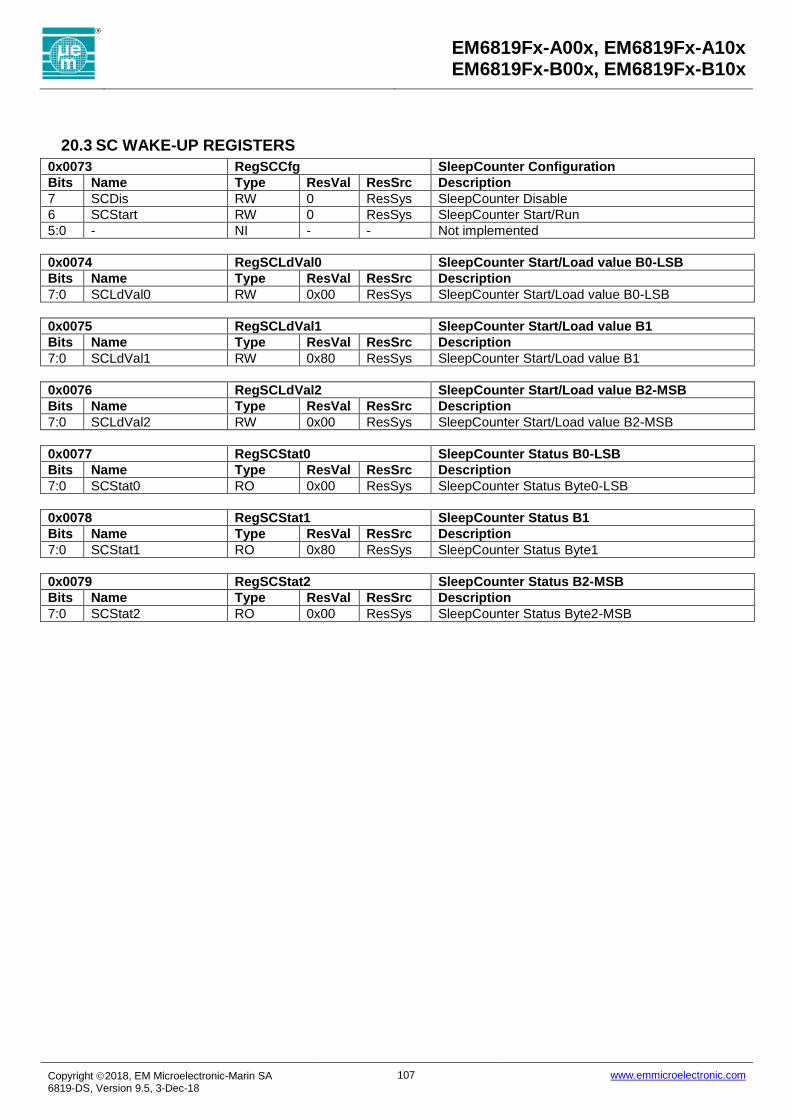
EM6819Fx-A00x, EM6819Fx-A10x EM6819Fx-B00x, EM6819Fx-B10x
Copyright 2018, EM Microelectronic-Marin SA 6819-DS, Version 9.5, 3-Dec-18
107 www.emmicroelectronic.com
20.3 SC WAKE-UP REGISTERS
0x0073 RegSCCfg SleepCounter Configuration
Bits Name Type ResVal ResSrc Description
7 SCDis RW 0 ResSys SleepCounter Disable
6 SCStart RW 0 ResSys SleepCounter Start/Run
5:0 - NI - - Not implemented
0x0074 RegSCLdVal0 SleepCounter Start/Load value B0-LSB
Bits Name Type ResVal ResSrc Description
7:0 SCLdVal0 RW 0x00 ResSys SleepCounter Start/Load value B0-LSB
0x0075 RegSCLdVal1 SleepCounter Start/Load value B1
Bits Name Type ResVal ResSrc Description
7:0 SCLdVal1 RW 0x80 ResSys SleepCounter Start/Load value B1
0x0076 RegSCLdVal2 SleepCounter Start/Load value B2-MSB
Bits Name Type ResVal ResSrc Description
7:0 SCLdVal2 RW 0x00 ResSys SleepCounter Start/Load value B2-MSB
0x0077 RegSCStat0 SleepCounter Status B0-LSB
Bits Name Type ResVal ResSrc Description
7:0 SCStat0 RO 0x00 ResSys SleepCounter Status Byte0-LSB
0x0078 RegSCStat1 SleepCounter Status B1
Bits Name Type ResVal ResSrc Description
7:0 SCStat1 RO 0x80 ResSys SleepCounter Status Byte1
0x0079 RegSCStat2 SleepCounter Status B2-MSB
Bits Name Type ResVal ResSrc Description
7:0 SCStat2 RO 0x00 ResSys SleepCounter Status Byte2-MSB

EM6819Fx-A00x, EM6819Fx-A10x EM6819Fx-B00x, EM6819Fx-B10x
Copyright 2018, EM Microelectronic-Marin SA 6819-DS, Version 9.5, 3-Dec-18
108 www.emmicroelectronic.com
21. 10-BITS ADC Two blocks compose the ADC:
The conditioner
The ADC converter The conditioner allows sampling different range of analog inputs even signal having a dynamic higher than VSUP. It consists to decrease the reference and the analog input in a range adapted for the ADC converter.
21.1 CONDITIONER
21.1.1 RANGE SELECTION
It consists to attenuate the external analog input range and external reference. It is used to adapt external range to internal range limited to maximum 1.7V as illustrated in the following diagram.
Vref_ext max
Vref_ext min
Vref_int min
Vref_int max
vss
Min
imum
exte
rnal ra
nge
Ma
xim
um
exte
rna
l ra
nge
Min
imum
inte
rna
l
ran
ge
Ma
xim
um
in
tern
al ra
nge
Vref_ext max
Vref_ext min
Vref_int min
Vref_int max
vss
Min
imum
exte
rnal ra
nge
Ma
xim
um
exte
rna
l ra
nge
Min
imum
inte
rna
l
ran
ge
Ma
xim
um
in
tern
al ra
nge
Vref_ext max: Maximum external range Vref_ext min: Minimum external range Vref_int max: Maximum internal range = 1.7V Vref_int min: Minimum internal range = 1.1V
External reference and attenuation factor called range shall be calculated to get an internal refenrence in a window of 1.1V to 1.7V. There is another condition to fullfil; the maximum external reference shall not be above VSUP if VSUP > VREG. If VSUP < VREG the maximum external reference is 1.7V. There are 4 possible ranges. The factor shall be chosen to get an internal reference in the window of 1.1V to 1.7V according to the following table:
Range Vref_ext min Vref_ext max
8/8 1.10 V 1.70 V
6/8 1.47 V 2.27 V
4/8 2.20 V 3.40 V
3/8 2.93 V 3.60 V (1)
(1) The maximum external range is limitated by maximum power supply 3.6V
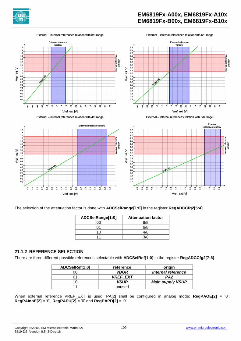
EM6819Fx-A00x, EM6819Fx-A10x EM6819Fx-B00x, EM6819Fx-B10x
Copyright 2018, EM Microelectronic-Marin SA 6819-DS, Version 9.5, 3-Dec-18
109 www.emmicroelectronic.com
0.1
0.2
0.3
0.4
0.5
0.6
0.7
0.8
0.9
1.0
1.1
0.2
0.4
0.6
0.8
1.0
1.2
1.4
1.6
1.8
2.0
2.2
2.4
2.6
2.8
3.0
3.2
3.4
3.6
1.2
1.3
1.4
1.5
1.6
1.7
1.8
1.9
Inte
rnal re
fere
nce
win
do
w
rang
e 8/
8External reference
window
External – internal references relation with 8/8 range
Vref_ext [V]
Vre
f_in
t [V
]
0.1
0.2
0.3
0.4
0.5
0.6
0.7
0.8
0.9
1.0
1.1
0.2
0.4
0.6
0.8
1.0
1.2
1.4
1.6
1.8
2.0
2.2
2.4
2.6
2.8
3.0
3.2
3.4
3.6
1.2
1.3
1.4
1.5
1.6
1.7
1.8
1.9
Inte
rnal re
fere
nce
win
do
w
rang
e 8/
8External reference
window
External – internal references relation with 8/8 range
Vref_ext [V]
Vre
f_in
t [V
]
0.1
0.2
0.3
0.4
0.5
0.6
0.7
0.8
0.9
1.0
1.1
0.2
0.4
0.6
0.8
1.0
1.2
1.4
1.6
1.8
2.0
2.2
2.4
2.6
2.8
3.0
3.2
3.4
3.6
1.2
1.3
1.4
1.5
1.6
1.7
1.8
1.9
Inte
rnal re
fere
nce
win
do
w
rang
e 6/
8
External reference
window
External – internal references relation with 6/8 range
Vref_ext [V]
Vre
f_in
t [V
]
0.1
0.2
0.3
0.4
0.5
0.6
0.7
0.8
0.9
1.0
1.1
0.2
0.4
0.6
0.8
1.0
1.2
1.4
1.6
1.8
2.0
2.2
2.4
2.6
2.8
3.0
3.2
3.4
3.6
1.2
1.3
1.4
1.5
1.6
1.7
1.8
1.9
Inte
rnal re
fere
nce
win
do
w
range 4/8
External reference window
External – internal references relation with 4/8 range
Vref_ext [V]
Vre
f_in
t [V
]
0.1
0.2
0.3
0.4
0.5
0.6
0.7
0.8
0.9
1.0
1.1
0.2
0.4
0.6
0.8
1.0
1.2
1.4
1.6
1.8
2.0
2.2
2.4
2.6
2.8
3.0
3.2
3.4
3.6
1.2
1.3
1.4
1.5
1.6
1.7
1.8
1.9
Inte
rnal re
fere
nce
win
do
w
range 4/8
External reference window
External – internal references relation with 4/8 range
Vref_ext [V]
Vre
f_in
t [V
]
0.1
0.2
0.3
0.4
0.5
0.6
0.7
0.8
0.9
1.0
1.1
0.2
0.4
0.6
0.8
1.0
1.2
1.4
1.6
1.8
2.0
2.2
2.4
2.6
2.8
3.0
3.2
3.4
3.6
1.2
1.3
1.4
1.5
1.6
1.7
1.8
1.9
Inte
rnal re
fere
nce
win
do
w
range 3/8
External
reference window
External – internal references relation with 3/8 range
Vref_ext [V]
Vre
f_in
t [V
]
0.1
0.2
0.3
0.4
0.5
0.6
0.7
0.8
0.9
1.0
1.1
0.2
0.4
0.6
0.8
1.0
1.2
1.4
1.6
1.8
2.0
2.2
2.4
2.6
2.8
3.0
3.2
3.4
3.6
1.2
1.3
1.4
1.5
1.6
1.7
1.8
1.9
Inte
rnal re
fere
nce
win
do
w
range 3/8
External
reference window
External – internal references relation with 3/8 range
Vref_ext [V]
Vre
f_in
t [V
]
The selection of the attenuation factor is done with ADCSelRange[1:0] in the register RegADCCfg2[5:4].
ADCSelRange[1:0] Attenuation factor
00 8/8
01 6/8
10 4/8
11 3/8
21.1.2 REFERENCE SELECTION
There are three different possible references selectable with ADCSelRef[1:0] in the register RegADCCfg2[7:6].
ADCSelRef[1:0] reference origin
00 VBGR Internal reference
01 VREF_EXT PA2
10 VSUP Main supply VSUP
11 unused -
When external reference VREF_EXT is used, PA[2] shall be configured in analog mode: RegPAOE[2] = ‘0’, RegPAInpE[2] = ‘0’, RegPAPU[2] = ‘0’ and RegPAPD[2] = ‘0’.

EM6819Fx-A00x, EM6819Fx-A10x EM6819Fx-B00x, EM6819Fx-B10x
Copyright 2018, EM Microelectronic-Marin SA 6819-DS, Version 9.5, 3-Dec-18
110 www.emmicroelectronic.com
Note: Always allow the reference voltage to stabilize before starting an ADC measure. When running on the internal reference this stabilization time is 130us from ADCEn until stable reference voltage. It is possible to start the reference prior to enabling of the ADC, refer to 24.
21.1.3 ANALOG INPUT SELECTION
There are 9 possible analog inputs selectable with ADCSelSrc[2:0] in register ADCOut1[6:4]. When the temperature sensor is active (EnTempSens in register RegADCCfg1[4] = ‘1’) the temperature sensor is automatically set as ADC analog input. StsTempSens in register RegADCOut1[3] is a copy of EnTempSens and is not writable. It allows checking if the temperature sensor is enable at each read of ADC data output.
EnTempSens ADCSelSrc[2:0] ADC source
0 000 PA0
0 001 PC0
0 010 PA1
0 011 PC1
0 100 PA2
0 101 PC2
0 110 PA3
0 111 PC3
1 xxx temperature sensor
21.2 ADC OFFSET TRIM SELECTION
Depending on the ADC configuration or if the ADC is used with the temperature sensor, the ADC offset shall be set differently. When the internal voltage is used, the ADC range selection has effect only on the analog input signal. Then the offset has to be adapted to the selected range. There is also a dedicated offset trim word used when the analog input is the temperature sensor in order to remove the offset error introduced by the sensor itself. All these trimming words are contained in the row 62 sector 5 of the NVM (refer to the chapter 3.6). The offset trim to use according to the configuration is as follows:
ADC configuration ADC offset trim DM address
ADC ref = internal Vref Range 3/8
ADCOffsetRng3_8[10:0] MSB 0x6FD1[10:8] LSB 0x6FD0[7:0]
ADC ref = internal Vref Range 4/8
ADCOffsetRng4_8[10:0] MSB 0x6FCF[10:8] LSB 0x6FCE[7:0]
ADC ref = internal Vref Range 6/8
ADCOffsetRng6_8[10:0] MSB 0x6FCD[10:8] LSB 0x6FCC[7:0]
Temperature sensor ADCOffsetTemp[10:0] MSB 0x6FC9[10:8] LSB 0x6FC8[7:0]
All other configurations ADCOffsetRng8_8[10:0] MSB 0x6FCB[10:8] LSB 0x6FCA[7:0]
The trimming word has to be copied from the NVM to the related registers: MSB in RegADCOffsetM DM address 0x005A and LSB in RegADCOffsetL DM address 0x0059. Note: ADC offset is coded and memorized in NVM on 11 bits. Their value can be above 0x3FF.

EM6819Fx-A00x, EM6819Fx-A10x EM6819Fx-B00x, EM6819Fx-B10x
Copyright 2018, EM Microelectronic-Marin SA 6819-DS, Version 9.5, 3-Dec-18
111 www.emmicroelectronic.com
ADC configurations
21.2.1 RUNNING MODE
The 6819 ADC has two possible running modes:
Continuous mode: the ADC runs continuously until the software stopps it.
One shot mode: the ADC makes just one single acquisition. To start the ADC in continuous mode, RunContMeas in register RegADCCfg1[6] shall be set at ‘1’. To start a single sample, RunSinglMeas in register RegADCCfg1[5] shall be set at ‘1’. Continuous mode has the priority over single measurement. Always fully define the ADC setup before starting any ADC measurement.
21.2.2 ADC ENABLING
Before to start an acquisition, EnADC in register RegADCCfg1[7] shall be set at ‘1’. When the ADC is stopped in continuous mode, EnADC shall be set at ‘0’ before to launch any other acquisition otherwise all next measurement will be corrupted. Note: EnADC will also enable the bandgap reference voltage. If the BGR is used as ADC reference the user must wait for the BGR to stabilize before starting any measurement. Refer to 24. If an external reference is used or the BGR was already enabled before - and is stabilized - still allow 5us setup time from EnADC to start of measuring.

EM6819Fx-A00x, EM6819Fx-A10x EM6819Fx-B00x, EM6819Fx-B10x
Copyright 2018, EM Microelectronic-Marin SA 6819-DS, Version 9.5, 3-Dec-18
112 www.emmicroelectronic.com
21.2.3 ADC SAMPLING RATE
The ADC can select 8 different sampling rates. ADC is running on Ck_Hi whatever the clock configuration. When the CPU and the Prescalers are not running on Ck_Hi, the clock for ADC shall be forced. Meaning that FrcEnRC15M or FrcEnRC2M or FrcEnExt shall be forced at ‘1’ and Ck_Hi shall be connected to the clock source forced. The maximum sampling rate of the ADC is 100kS/s, the ADC needs 22 clocks for each sample, than the maximum selectable ADC frequency is 2.2MHz. The clock selection is done with ADCSmplRate[2:0] in register RegADCCfg1[3:1]. Following table shows the relation between the clock source selection and the sampling rate.
ADCSmplRate[2:0] Clock division
factor
Sampling rate kS/s
Ck_Hi = 15MHz Ck_Hi = 2MHz Ck_Hi = 4MHz Xtal
000 1 (default) denied 90.91 denied
001 2 denied 45.45 90.91
010 4 denied 22.73 45.45
011 8 83.78 11.36 22.73
100 16 41.89 5.68 11.36
101 32 20.95 2.84 5.68
110 64 10.47 1.42 2.84
111 1 denied 90.91 denied
The first conversion shall be ignored. Then in single mode the conversion need 44 clocks. This is automatically managed by the 6819, the event is generated only after the second conversion. Following table shows the relation between the conversion duration and the clock source selection.
ADCSmplRate[2:0] Clock division
factor Conversion duration us
Ck_Hi = 15MHz Ck_Hi = 2MHz Ck_Hi = 4MHz Xtal
000 1 (default) denied 22.00 denied
001 2 denied 44.00 22.00
010 4 denied 88.00 44.00
011 8 23.87 176.00 88.00
100 16 47.74 352.00 176.00
101 32 95.49 704.00 352.00
110 64 190.97 1408.00 704.00
111 1 denied 22.00 denied
21.2.4 LOW NOISE MODE
There is two way to decrease the noise due to activity of 6819:
Force DC-DC in idle mode for a short time.
Make ADC acquisition only when the CPU is in halt mode. When the DC-DC is used, it is possible to stop it for a short time by setting DC-DCIdle in register RegDC-DCCfg[4] at ‘1’. In this case the only source of energy is the external capacitor. Then it is recommended to ensure that no big consumer is working when the DC-DC is in idle mode (refer to DC-DC chapter). As soon as the ADC convertion is done the DCDIdle shall be set at ‘0’ again. The ADC should be used only in one shot mode in this case to recharge the external capacitor between between each ADC acquisition. ADC low noise mode consists to start the ADC convertion only when the CPU is in stand by mode by setting ADCLowNoise in register RegADCCfg2[3] at ‘1’. The CPU is waked up by ADC event or ADC interrupt when the convertion is done and ADC result available if they are unmasked.
21.2.5 8BIT ADC SELECTION
It is possible to set the size of the ADC result between 10 or 8-bits. If high precision is not required, it allows simplifying the software as the data are in 8bit. In this case two LSB bits are lost. The other bits are shifted in register RegADCOut0[7:0]. In 10-bits mode the result is split in registers RegADCOut1[1:0] (2 MSB bits) and RegADCOut0[7:0] (8 LSB bits).

EM6819Fx-A00x, EM6819Fx-A10x EM6819Fx-B00x, EM6819Fx-B10x
Copyright 2018, EM Microelectronic-Marin SA 6819-DS, Version 9.5, 3-Dec-18
113 www.emmicroelectronic.com
21.3 ADC ACQUISITION SEQUENCE
The ADC generates an interrupt or an event when the acquisition is done and the result available for CPU. Thank to the event it is possible to force the CPU in std-by mode, the event wake-up the CPU automatically when the ADC result is available. It allows in continuous saving time because the CPU does not need to go through the handler. It is also possible to react by polling the event with conditional jump JEV. Int0StsADC in register RegInt0Sts[4] is the interrupt generated at the end of each acquisition. Evt1StsADC in register RegEvtSts[1] is the event generated at the end of each acquisition. The ADC result is available in registers RegADCOut1[1:0] (2 MSB bits) and RegADCOut0[7:0] (8 LSB bits). To ensure that a new acquisition between reading RegADCOut1[1:0] and RegADCOut0[7:0] does not corrupt the ADC result, RegADCOut0[7:0] is stored in a shadow register when RegADCOut1[1:0] is read. Both registes are read in fact exactly in the same time. RegADCOut1[1:0] shall always be read first. RegADCOut1.ADCOutLSB is the 11th bits result LSB and it is not guaranteed. The bit ADCBusy in read-only register RegADCOut1[7] is at ‘1’ when the ADC is working. It allows detecting the end of acquisition in one shot mode by polling.
21.4 ADC REGISTERS
0x0055 RegADCCfg1 ADC Configuration - 1
Bits Name Type ResVal ResSrc Description
7 EnADC RW 0 ResSys Enable ADC Block
6 RunContMeas RW 0 ResSys Run Continues measurement
5 RunSinglMeas STS 0 ResSys Run/Start Single measurement
4 EnTempSens RW 0 ResSys Enable Temperature Sensor
3:1 ADCSmplRate RW '000' ResSys ADC Sample Rate setup - continues mode.
0 ADC8bit RW 0 ResSys ADC 8bit Result mode
0x0056 RegADCCfg2 ADC Configuration - 2
Bits Name Type ResVal ResSrc Description
7:6 ADCSelRef RW '00' ResSys ADC Reference selection
5:4 ADCSelRange RW '00' ResSys ADC Range selection
3 ADCLowNoise RW 0 ResSys ADC Low noise measurement mode
2:0 - NI - - Not implemented
0x0057 RegADCOut0 ADC Output-0 (LSB)
Bits Name Type ResVal ResSrc Description
7:0 ADCOut0 RO 0x00 ResSys ADC Output-0: 10bit=LSB(8:1), 8bit-(10:3)
0x0058 RegADCOut1 ADC Output-1 (MSB)
Bits Name Type ResVal ResSrc Description
7 ADCBusy RO 0 ResSys ADC in progress
6:4 ADCSelSrc RW '000' ResSys ADC Input Source selection
3 StsTempSens RO 0 ResSys Enable Temperature Sensor Status
2 ADCOutLSB RO 0 ResSys ADC Output HW-LSB(0)
1:0 ADCOut1 RO '00' ResSys ADC Output-1: 10bit-MSB(10:9), 8bit-N/A
0x0059 RegADCOffsetL ADC Offset LSB (7:0)
Bits Name Type ResVal ResSrc Description
7:0 ADCOffsetL RW 0x00 ResSys ADC Offset LSB (7:0)
0x005A RegADCOffsetM ADC Offset MSB (10:8)
Bits Name Type ResVal ResSrc Description
7:3 - NI - - Not implemented
2:0 ADCOffsetM RW '100' ResSys ADC Offset MSB (10:8)

EM6819Fx-A00x, EM6819Fx-A10x EM6819Fx-B00x, EM6819Fx-B10x
Copyright 2018, EM Microelectronic-Marin SA 6819-DS, Version 9.5, 3-Dec-18
114 www.emmicroelectronic.com
22. TEMPERATURE SENSOR
22.1 TEMPERATURE SENSOR ENABLING
The temperature sensor is enabled when EnTempSens in register RegADCCfg1 is written at ‘1’. When the temperature sensor is enabled it is automatically selected by the ADC as input source. Read-only bit StsTempSens in register RegADCOut1 is a copy of EnTempSens. Thank to it the status of temperature sensor is given on each ADC result read access.
22.2 TEMPERATURE SENSOR REGISTERS
0x0055 RegADCCfg1 ADC Configuration - 1
Bits Name Type ResVal ResSrc Description
7 EnADC RW 0 ResSys Enable ADC Block
6 RunContMeas RW 0 ResSys Run Continues measurement
5 RunSinglMeas STS 0 ResSys Run/Start Single measurement
4 EnTempSens RW 0 ResSys Enable Temperature Sensor
3:1 ADCSmplRate RW '000' ResSys ADC Sample Rate setup - continues mode.
0 ADC8bit RW 0 ResSys ADC 8bit Result mode
0x0058 RegADCOut1 ADC Output-1 (MSB)
Bits Name Type ResVal ResSrc Description
7 ADCBusy RO 0 ResSys ADC in progress
6:4 ADCSelSrc RW '000' ResSys ADC Input Source selection
3 StsTempSens RO 0 ResSys Enable Temperature Sensor Status
2 ADCOutLSB RO 0 ResSys ADC Output HW-LSB(0)
1:0 ADCOut1 RO '00' ResSys ADC Output-1: 10bit-MSB(10:9), 8bit-N/A
Note: Temperature sensor calibration values are stored in row 62 sector 5 as described in chapter 4.6. Temperature tolerances of production test are described in chapter 4.6.1. When EnTempSens is written at ‘1’ it is necessary to wait 10ms before to launch an ADC acquisition.

EM6819Fx-A00x, EM6819Fx-A10x EM6819Fx-B00x, EM6819Fx-B10x
Copyright 2018, EM Microelectronic-Marin SA 6819-DS, Version 9.5, 3-Dec-18
115 www.emmicroelectronic.com
23. DC/DC CONVERTER The DC-DC converter allows supplying the chip and external elements on the board using a low voltage supply source. The DC-DC converter is not enabled by default but by the software. 6819 is able to start-up with a low voltage supply using the internal voltage multiplier. As the voltage multiplier is not able to deliver more than 100uA, it is recommended to enable the DC-DC before to enable the big consumers.
23.1 DC/DC ENABLING
Enable the DC-DC consists to write ‘1’ in EnDC-DC in register RegDC-DCCfg[7]. During the start-up phase of DC-DC the read-only bit DC-DCStartSts in RegDC-DCCfg[3] is at ‘1’. The current driven shall not exceed 10mA during the start-up phase.
23.2 DC/DC VOLTAGE SELECTION
There are 4 target voltages selectable with DC-DCLevel[1:0] in register RegDC-DCCfg[6:5]. It is possible to change the voltage level of DC-DC on the fly while DC-DC is enabled but when the voltage rise up the current driven shall not exceed 10mA.
DC-DCLevel[1:0] Voltage level
0x00 2.1
0x01 2.5
0x10 2.9
0x11 3.3
23.3 DC/DC LOW NOISE MODE
The noise level generated by the DC-DC converter can possibly influence precise voltage monitoring on VLD and ADC. To avoid such noise influence the DC-DC converter can be put in IDLE mode during such measurements. The IDLE duration is purely software controlled. Writing ‘1’ in DC-DCIdle in register RegDC-DCCfg[4] force the DC-DC off, in this mode the external capacitance becomes the only source of energy. Then the big consumer shall be switched off when DC-DCIdle is set to ‘1’. It is recommended to use the VLD to supervise VSUP and switch the DC-DC on when the supply is to low. The time the DC-DC can be in idle is related to the maximum voltage drop on VSUP, the external capacitor value and the current consumption as follows.
TDC-DCIdle: Delay in idle mode Cext: External capacitor value
VSUP: Drop on VSUP ISUP: Current consumption on VSUP
Note: The DC-DC – Step-Up converter does not allow Voltage down conversion.
SUP
EXTDCDCIdle
I
VSUPCT

EM6819Fx-A00x, EM6819Fx-A10x EM6819Fx-B00x, EM6819Fx-B10x
Copyright 2018, EM Microelectronic-Marin SA 6819-DS, Version 9.5, 3-Dec-18
116 www.emmicroelectronic.com
23.4 DC-DC REGISTER
0x005D RegDC-DCCfg DC-DC Configuration
Bits Name Type ResVal ResSrc Description
7 EnDC-DC RW 0 ResAna Enable DC-DC
6:5 DC-DCLevel RW '00' ResAna Select DC-DC Output Level
4 DC-DCIdle RW 0 ResAna DC-DC Idle mode
3 DC-DCStartSts RO 0 DC-DC Start-up status
2:0 - NI - - Not implemented
EM6819Fx-A00x, EM6819Fx-A10x EM6819Fx-B00x, EM6819Fx-B10x
Copyright 2018, EM Microelectronic-Marin SA 6819-DS, Version 9.5, 3-Dec-18
117 www.emmicroelectronic.com
24. BAND GAP The band gap voltage reference, written also BGR in this document, generates the reference voltage used for the following peripherals:
VLD (while VLD enabled)
ADC, (while ADC enabled CPU in active or standby mode)
DC-DC, (while DCDC enabled)
OPAMP (while OPAMP enabled and the BGR or the VLD reference is selected as one of the OPAMP inputs
BGR output on PA[6], (while the reference voltage is output)
NVM memory modification (fully controlled by ROM-API) First time enabled allow for 130us reference voltage stabilization time before using one of the above mention functions needing the BGR voltage. The reference voltage is automatically enabled as soon as one of the above mentioned functions is enabled. The reference voltage can be forced on by writing the bit NVMEnWrite in register RegBgrCfg[6] to ‘1’ prior to use it for destination function. This allows using the VLD and ADC immediately after enabling (no need to wait first for BGR stabilization). The BGR can be used as an external reference as well. Writing ‘1’ in BgrEnOut in register RegBgrCfg[7] connects the voltage reference to PA[6] that shall be configured as analog pad before (digital output and input mode off and no pull’s).
24.1 BAND GAP REGISTER
0x0060 RegBgrCfg BandGap reference configuration
Bits Name Type ResVal ResSrc Description
7 BgrEnOut RW 0 ResSys Enable BandGap reference output to Port
6 NVMEnWrite RW 0 ResSys Enables BandGap in active mode
5:0 - NI - - Not implemented
Note: When connecting the reference voltage to the PA[6] output , the reference voltage may drop during the switching transition due to charge sharing from the internal reference voltage node to the external PA[6] pad and its attached capacitance. In this case the settling time can be longer than 130us. Always use the reference voltage only once it is completely stabilized.

EM6819Fx-A00x, EM6819Fx-A10x EM6819Fx-B00x, EM6819Fx-B10x
Copyright 2018, EM Microelectronic-Marin SA 6819-DS, Version 9.5, 3-Dec-18
118 www.emmicroelectronic.com
25. VLD The Voltage Level Detector (VLD) compares a voltage on a terminal pad to a fix reference and returns the result ‘1’ or generates an interrupt if the voltage is below the reference. The measurement is static meaning that there is no need to start any sequence and the selected voltage source terminal is continuously supervised. The reference voltage VVLD is factory pretrimmed.
25.1 VLD SOURCE AND LEVEL SELECTION
There are 8 terminals selectable with VLDSelSrc[2:0] in register RegVLDCfg1[5:3] as follows:
VLDSelSrc[2:0] Source
000 VSUP (default)
001 PA1
010 PA2
011 PC1
100 PC5
101 PA6
110 PC6
111 PA7
The are 32 target level selectable with VLDSelLev[4:0] in register RegVLDCfg2[4:0] as follows:
Refer to the electricalspecification for the voltage levels (spread from 0.8V to 3.0V)
VLDSelLev[4:0] Level VLDSelLev[4:0] Level [V]
00000 VLD0 10000 VLD16
00001 VLD1 10001 VLD17
00010 VLD2 10010 VLD18
00011 VLD3 10011 VLD19
00100 VLD4 10100 VLD20
00101 VLD5 10101 VLD21
00110 VLD6 10110 VLD22
00111 VLD7 10111 VLD23
01000 VLD8 11000 VLD24
01001 VLD9 11001 VLD25
01010 VLD10 11010 VLD26
01011 VLD11 11011 VLD27
01100 VLD12 11100 VLD28
01101 VLD13 11101 VLD29
01110 VLD14 11110 VLD30
01111 VLD15 11111 VLD31
25.2 VLD ENABLE
VLD is enable writing ‘1’ in EnVLD in register RegVLDCfg1[7]. After enabling it is recommended to wait 150us before enabling the related interrupt or read the VLD result to allow the reference voltage to stabilize. This stabilization wait is only needed if the internal BGR voltage was not enabled for 150us prior to enabling the VLD. If the BGR was already enabled before still allow 20us for the VLD reference to stabilize after VLD enabling. Refer also to 24.
25.3 VLD RESULT
When the voltage measured is below the VLD level the read-only bit VLDRes in register RegVLDCfg1[6] is at ‘1’.

EM6819Fx-A00x, EM6819Fx-A10x EM6819Fx-B00x, EM6819Fx-B10x
Copyright 2018, EM Microelectronic-Marin SA 6819-DS, Version 9.5, 3-Dec-18
119 www.emmicroelectronic.com
25.4 VLD INTERRUPT
An interrupt is generated when the voltage measured is below the VLD level. The VLD interrupt IntSts2Vld is in register RegInt2Sts[7].
25.5 VLD TRIMMING
The VLD reference voltage VVLD is trimmed in production independently of the BGR. The trimming value is stored in the NVM at the address 0x6FF9. During the boot ROM sequence this value is copied in TrimVLD[3:0] in register RegTrimVLD. The user can modify this register to move slightly all VLD levels.
25.6 VLD REGISTERS
0x005E RegVLDCfg1 VLD Configuration - 1
Bits Name Type ResVal ResSrc Description
7 EnVLD RW 0 ResSys Enable VLD
6 VLDRes RO 0 ResSys VLD Result/Output
5:3 VLDSelSrc RW '000' ResSys Select VLD Input/Source
2:0 - NI - - Not implemented
0x005F RegVLDCfg2 VLD Configuration - 2
Bits Name Type ResVal ResSrc Description
7:5 - NI - - Not implemented
4:0 VLDSelLev RW 0x00 ResSys Select VLD Level
0x02A4 RegTrimVLD Trimming value for VLD
Bits Name Type ResVal ResSrc Description
7:4 - NI - - Not implemented
3:0 TrimVLD RW 0x8 ResAna Trimming value for VLD

EM6819Fx-A00x, EM6819Fx-A10x EM6819Fx-B00x, EM6819Fx-B10x
Copyright 2018, EM Microelectronic-Marin SA 6819-DS, Version 9.5, 3-Dec-18
120 www.emmicroelectronic.com
26. RC OSCILLATOR There are 2 main internal RC oscillators:
15MHz oscillator (runs at 14.7456 MHz but called 15MHz oscillator)
2MHz oscillator Thes 2 oscillators are factory pretrimmed, the trim value is stored in the NVM at the following addresses:
15MHz oscillator: 0x6FFD
2MHz oscillator: 0x6FFC The boot ROM sequence copies the 15MHz trimming value from the NVM into TrimOsc15M in register RegTrimOsc15M and the 2MHz trimming value from the NVM into TrimOsc2M in register RegTrimOsc2M. The user can modify these two trimming in their destination register RegTrimOsc15M, RegTrimOsc2M. Note: Before any CALL of sub-routine erasing or writing the NVM, the default RC timming values from NVM shall be restored.
26.1 RC OSCILLATORS REGISTERS
0x02A2 RegTrimOsc15M Trimming value for the 15 MHz Oscillator
Bits Name Type ResVal ResSrc Description
7:0 TrimOsc15M RW 0x80 ResAna Trimming value for the 15 MHz Oscillator
0x02A3 RegTrimOsc2M Trimming value for the 2 MHz Oscillator
Bits Name Type ResVal ResSrc Description
7:0 TrimOsc2M RW 0x80 ResAna Trimming value for the 2 MHz Oscillator

EM6819Fx-A00x, EM6819Fx-A10x EM6819Fx-B00x, EM6819Fx-B10x
Copyright 2018, EM Microelectronic-Marin SA 6819-DS, Version 9.5, 3-Dec-18
121 www.emmicroelectronic.com
27. XTAL OSCILLATOR 32KHZ XTAL oscillator is connected to the terminal pads PA4 (XIN) and PC4 (XOUT). These two pads shall be configured in analog mode (output and input mode disable and no pull’s) before to launch the XTAL oscillator. Note: The XTAL oscillator shall be located as close as possible to the 6819. Both wires XIN and XOUT shall be routed as short as possible on the board. For all information concerning the different configuration related to the 32 KHz XTAL oscillator, refer to the chapter “Oscillator and Clocking structure”.

EM6819Fx-A00x, EM6819Fx-A10x EM6819Fx-B00x, EM6819Fx-B10x
Copyright 2018, EM Microelectronic-Marin SA 6819-DS, Version 9.5, 3-Dec-18
122 www.emmicroelectronic.com
28. RESONATOR 4MHZ RC resonator is connected to the terminal pads PA4 (XIN) and PC4 (XOUT). These two pads shall be configured in analog mode (output and input mode disable and no pull’s) before to launch the resonator. Note: The Resonator shall be located as close as possible to the 6819. Both wires XIN and XOUT shall be routed as short as possible on the board. Two capacitors of 39pF shall be implemented on the board. The first between XIN and VSS, the second between XOUT and VSS as describe in the following schematic:
XIN XOUT
39pF 39pF
Cp
Cs
Ls
Rs
XIN XOUT
39pF 39pF
Cp
Cs
Ls
Rs
For all information concerning the different configuration related to the 4MHz resonator, refer to the chapter “Oscillator and Clocking structure”.

EM6819Fx-A00x, EM6819Fx-A10x EM6819Fx-B00x, EM6819Fx-B10x
Copyright 2018, EM Microelectronic-Marin SA 6819-DS, Version 9.5, 3-Dec-18
123 www.emmicroelectronic.com
29. 8KHZ OSCILLATOR The 8kHz oscillator is used mainly for the watch-dog and the sleep counter wake-up system. Its frequency is not trimmable. However timings generated by the 8kHz oscillator can be calibrated with the trimmed 2Mhz or 15Mhz oscillator. For very low power applications it is also possible possible to use the 8kHz oscillator for the CPU and the prescalers For all information concerning the different configuration related to the 8kHz oscillator, refer to the chapter “Oscillator and Clocking structure”.

EM6819Fx-A00x, EM6819Fx-A10x EM6819Fx-B00x, EM6819Fx-B10x
Copyright 2018, EM Microelectronic-Marin SA 6819-DS, Version 9.5, 3-Dec-18
124 www.emmicroelectronic.com
30. ANALOG OPAMP Each pin of the OPAMP in 6819 can be connected to different terminal or other peripherals. The positive input selection is done with OpAmpSelInpPos[1:0] in register RegOpAmpCfg2[7:0] as following:
OpAmpSelInpPos[1:0] positive input
00 PA3
01 PC3
10 VBGR
11 VVLD
The negative input selection is done with OpAmpSelInpNeg[1:0] in register RegOpAmpCfg[7:0] as following:
OpAmpSelInpNeg[1:0] negative input
00 PA2
01 PC2
10 VBGR
11 VVLD
When the OPAMP is enable and comparator disable, the output can be mapped on to different terminal with OpAmpSelOut in register RegOpAmpCfg[3] as follows:
OpAmpSelOut output
0 PA1
1 PC1
30.1 SELECT OPAMP/COMPARATOR
To enable the OPAMP, EnOpAmp in register RegOpAmpCfg1[7] shall be set at ‘1’. In this case the selected terminals are connected to the OPAMP. The terminal shall be configure in analog mode before to enable the OPAMP, it is not done automatically (output and input mode disable and no pull’s). To enable the comparator EnOpAmp in register RegOpAmpCfg1[7] and EnComp in register RegOpAmpCfg1[6] shall set at ‘1’. In this mode the output is not mapped on any of the two terminals PA1 or PC1.
30.2 SUPPLY SELECTION
The OPAMP and the comparator are able to work under VREG or VSUP voltage to be able to select two different swings. Even when 6819 is supplied at 0.9V it is possible to get a swing of 1.6V if the OPAMP is supplied by VREG. When OpAmpSup in register RegOpAmpCfg1 is at ‘0’ VSUP is selected, if it is at ‘1’ VREG is selected.
VSUP VREG
EnOpamp
SelOpampSup
CompRes
IntOpAmp
EnComp
PA2
PC2
VBGR
VVLD
PA3
PC3
VBGR
VVLD
OpaInpNeg
OpaInpPos
PA1
PC1
OpampOutSel
Opamp architecture
EnOpamp && !EnComp

EM6819Fx-A00x, EM6819Fx-A10x EM6819Fx-B00x, EM6819Fx-B10x
Copyright 2018, EM Microelectronic-Marin SA 6819-DS, Version 9.5, 3-Dec-18
125 www.emmicroelectronic.com
30.3 COMPARATOR RESULT
The comparator result is mapped on the read-only bit CompRes in register RegOpAmpCfg1[4]. The comparator can generate an interrupt mapped on Int1StsOpAmp in register RegInt1Sts[3]. It is possible to set on which edge the interrupt is generated with SelCompInt[1:0] in register RegOpAmpCfg1[3:2] as follows:
SelCompInt[1:0] interrupt generation
00 no interrupt
01 interrupt on rising edge
10 interrupt on falling edge
11 interrupt on both edges
30.4 OPAMP REGISTERS
0x005B RegOpAmpCfg1 OpAmp Configuration - 1
Bits Name Type ResVal ResSrc Description
7 EnOpAmp RW 0 ResSys Enable OP Amplifier
6 EnComp RW 0 ResSys Enable/Select OpAmp as Comparator
5 OpAmpSup RW 0 ResSys OpAmp Supply: 0-Vbat, 1-Vreg
4 CompRes RO 0 ResSys Comparator Result
3:2 SelCompInt RW '00' ResSys Selector/Enable of Comparator Interrupt
1:0 - NI - - Not implemented
0x005C RegOpAmpCfg2 OpAmp Configuration - 2
Bits Name Type Bits Name Type
7:6 OpAmpSelInpPos[1:0] RW 0 ResAna Select opamp positive input source
5:4 OpAmpSelInpNeg[1:0] RW 0 ResAna Select opamp negative input source
3 OpAmpSelOut RW 0 ResAna Select opamp output pad
2:0 - NI - - Not implemented

EM6819Fx-A00x, EM6819Fx-A10x EM6819Fx-B00x, EM6819Fx-B10x
Copyright 2018, EM Microelectronic-Marin SA 6819-DS, Version 9.5, 3-Dec-18
126 www.emmicroelectronic.com
31. BLOCKS CONSUMPTION Following table shows the consumption of different blocks of EM6819 in typical conditions. Consumption of system, CPU, NVM access etc… have been excluded for each block to get only the consumption of the block itself. Temperature: 25°C VSUP: 3V
Block Consumption Special conditions
Brown-out 600 nA
Watch-dog 40 nA
Sleep counter wake-up 90 nA
RC 15 MHz 23 uA
RC 2 MHz 6 uA
RC 8 kHz 90 nA
Xtal 400 nA
BGR 11 uA
VLD 7.2 uA VLD source: VSUP VLD level: 0
ADC 50 uA Sampling rate: 12.5 kS/s Range: 8/8 Reference: BGR (Not included in consumption) ADC Input: PC1 = 0.618 V (Vref / 2)
OpAmp 52 uA Comparator mode: Off OpAmp supply: VSUP Input neg: PA2 = 0V Input pos: PA3 = VSUP (3V) Output: PC1 = VSUP (3V)
18 uA Comparator mode: Off OpAmp supply: VSUP Input neg: PA2 = VSUP (3V) Input pos: PA3 = 0V Output: PC1 = 0V
Timers 26 uA Timer1 consumption considered CPU clock: 8kHz Prescaler1 clock: 2 MHz Prescaler2 clock: 8 kHz Timer1 clock: Prescaler1 Ck15 (2 MHz)
SPI 16 uA SPI mode: Master, Auto start SCLK clock: 2 MHz (not mapped on any pad) SIN: PA4 = 0V SOUT: Not mapped on any pad Sequence: Write 0xAA ; 0x55 continously in RegSPIDOut

EM6819Fx-A00x, EM6819Fx-A10x EM6819Fx-B00x, EM6819Fx-B10x
Copyright 2018, EM Microelectronic-Marin SA 6819-DS, Version 9.5, 3-Dec-18
127 www.emmicroelectronic.com
32. TYPICAL T AND V DEPENDENCIES
32.1 IDD CURRENTS
32.1.1 GENERAL CONDITIONS
Mode Description
Active CPU: running at selected clock Software: makes a loop and writes/reads continuously the RAM Prescaler1: Running on ck_hi when available otherwise ck_lo Prescaler2: Always running on ck_lo Brown-out: Enable Watch-dog: Running on 8kHz Regulator: Vreg = 1.8V enable ; multiplier enable when VSUP is low ; retention voltage off
Stand-by CPU: Halt state Software: No software executed Prescaler1: Running on ck_hi when available otherwise ck_lo Prescaler2: Always running on ck_lo Brown-out: Enable Watch-dog: Running on 8kHz Regulator: Vreg = 1.8V enable ; multiplier enable when VSUP is low ; retention voltage off
Sleep CPU: Halt state Software: No software executed Prescaler1: Disable Prescaler2: Disable Brown-out: Disable Watch-dog: Disable Regulator: Vreg = 1.8V enable ; multiplier off ; retention voltage enable
Power-down
CPU: Halt state Software: No software executed Prescaler1: Disable Prescaler2: Disable Brown-out: Disable Watch-dog: Disable Regulator: Vreg = 1.8V off ; multiplier off ; retention voltage off

EM6819Fx-A00x, EM6819Fx-A10x EM6819Fx-B00x, EM6819Fx-B10x
Copyright 2018, EM Microelectronic-Marin SA 6819-DS, Version 9.5, 3-Dec-18
128 www.emmicroelectronic.com
Figure 31, Temperature and supply dependency for consumption @ 15 MHz
Idd 15MHz active over VSUP
@ Temperature = 25°C
0
200
400
600
800
1000
1200
2.2 2.4 2.6 2.8 3 3.2 3.4 3.6
VSUP [V]
Idd
[u
A]
Idd 15MHz active over temperature
@ VSUP = 3V
0
200
400
600
800
1000
1200
-40 -20 0 20 40 60 80
Temperature [°C]
Idd
[u
A]
Idd 15MHz std-by over VSUP
@ Temperature = 25°C
0
10
20
30
40
50
60
70
80
90
100
2.2 2.4 2.6 2.8 3 3.2 3.4 3.6
VSUP [V]
Idd
[u
A]
Idd 15MHz std-by over temperature
@ VSUP = 3V
0
10
20
30
40
50
60
70
80
90
100
-40 -20 0 20 40 60 80
Temperature [°C]
Idd
[u
A]

EM6819Fx-A00x, EM6819Fx-A10x EM6819Fx-B00x, EM6819Fx-B10x
Copyright 2018, EM Microelectronic-Marin SA 6819-DS, Version 9.5, 3-Dec-18
129 www.emmicroelectronic.com
Figure 32, Temperature and supply dependency for consumption @ 2 MHz
Idd 2MHz active over VSUP
@ Temperature = 25°C
0
100
200
300
400
500
600
700
800
900
1000
0.9 1.4 1.9 2.4 2.9 3.4
VSUP [V]
Idd
[u
A]
Idd 2MHz active over temperature
@ VSUP = 3V
0
20
40
60
80
100
120
140
160
180
200
-40 -20 0 20 40 60 80
Temperature [°C]
Idd
[u
A]
Idd 2MHz std-by over VSUP
@ Temperature = 25°C
0
10
20
30
40
50
60
70
80
90
100
0.9 1.4 1.9 2.4 2.9 3.4
VSUP [V]
Idd
[u
A]
Idd 2MHz std-by over temperature
@ VSUP = 3V
0
2
4
6
8
10
12
14
16
18
20
-40 -20 0 20 40 60 80
Temperature [°C]
Idd
[u
A]

EM6819Fx-A00x, EM6819Fx-A10x EM6819Fx-B00x, EM6819Fx-B10x
Copyright 2018, EM Microelectronic-Marin SA 6819-DS, Version 9.5, 3-Dec-18
130 www.emmicroelectronic.com
Figure 33, Temperature and supply dependency for consumption @ 4 MHz resonator
Idd 4MHz resonator active over VSUP
@ Temperature = 25°C
0
50
100
150
200
250
300
350
400
450
500
2.2 2.4 2.6 2.8 3 3.2 3.4 3.6
VSUP [V]
Idd
[u
A]
Idd 4MHz resonator active over temperature
@ VSUP = 3V
0
50
100
150
200
250
300
350
400
450
500
-40 -20 0 20 40 60 80
Temperature [°C]
Idd
[u
A]
Idd 4MHz resonator std-by over VSUP
@ Temperature = 25°C
0
5
10
15
20
25
30
35
40
45
50
2.2 2.4 2.6 2.8 3 3.2 3.4 3.6
VSUP [V]
Idd
[u
A]
Idd 4MHz resonator std-by over temperature
@ VSUP = 3V
0
5
10
15
20
25
30
35
40
45
50
-40 -20 0 20 40 60 80
Temperature [°C]
Idd
[u
A]

EM6819Fx-A00x, EM6819Fx-A10x EM6819Fx-B00x, EM6819Fx-B10x
Copyright 2018, EM Microelectronic-Marin SA 6819-DS, Version 9.5, 3-Dec-18
131 www.emmicroelectronic.com
Figure 34, Temperature and supply dependency for consumption @ 32 kHz XTAL
Idd 32kHz active over VSUP
@ Temperature = 25°C
0
2
4
6
8
10
12
14
16
18
20
0.9 1.4 1.9 2.4 2.9 3.4
VSUP [V]
Idd
[u
A]
Idd 32kHz active over temperature
@ VSUP = 3V
0
1
2
3
4
5
6
7
8
9
-40 -20 0 20 40 60 80
Temperature [°C]
Idd
[u
A]
Idd 32kHz std-by over VSUP
@ Temperature = 25°C
0
1
2
3
4
5
6
7
8
9
10
0.9 1.4 1.9 2.4 2.9 3.4
VSUP [V]
Idd
[u
A]
Idd 32kHz std-by over temperature
@ VSUP = 3V
0
1
2
3
4
5
6
-40 -20 0 20 40 60 80
Temperature [°C]
Idd
[u
A]

EM6819Fx-A00x, EM6819Fx-A10x EM6819Fx-B00x, EM6819Fx-B10x
Copyright 2018, EM Microelectronic-Marin SA 6819-DS, Version 9.5, 3-Dec-18
132 www.emmicroelectronic.com
Figure 35, Temperature and supply dependency for consumption @ 8 kHz
Idd 8kHz active over VSUP
@ Temperature = 25°C
0
2
4
6
8
10
12
14
16
18
20
0.9 1.4 1.9 2.4 2.9 3.4
VSUP [V]
Idd
[u
A]
Idd 8kHz active over temperature
@ VSUP = 3V
0
1
2
3
4
5
6
7
-40 -20 0 20 40 60 80
Temperature [°C]
Idd
[u
A]
Idd 8kHz std-by over VSUP
@ Temperature = 25°C
0
2
4
6
8
10
12
14
16
18
20
0.9 1.4 1.9 2.4 2.9 3.4
VSUP [V]
Idd
[u
A]
Idd 8kHz std-by over temperature
@ VSUP = 3V
0
1
2
3
4
5
6
-40 -20 0 20 40 60 80
Temperature [°C]
Idd
[u
A]

EM6819Fx-A00x, EM6819Fx-A10x EM6819Fx-B00x, EM6819Fx-B10x
Copyright 2018, EM Microelectronic-Marin SA 6819-DS, Version 9.5, 3-Dec-18
133 www.emmicroelectronic.com
Figure 36, Temperature and supply dependency for consumption in sleep mode
Idd sleep without sleep counter wake-up over VSUP
@ Temperature = 25°C
0
0.5
1
1.5
2
2.5
3
3.5
4
4.5
5
0.9 1.4 1.9 2.4 2.9 3.4
VSUP [V]
Idd
[u
A]
Idd sleep without sleep counter wake-up over temperature
@ VSUP = 3V
0
0.5
1
1.5
2
2.5
3
3.5
4
4.5
5
-40 -20 0 20 40 60 80
Temperature [°C]
Idd
[u
A]
Idd sleep with sleep counter wake-up over VSUP
@ Temperature = 25°C
0
0.5
1
1.5
2
2.5
3
3.5
4
4.5
5
0.9 1.4 1.9 2.4 2.9 3.4
VSUP [V]
Idd
[u
A]
Idd sleep with sleep counter wake-up over temperature
@ VSUP = 3V
0
0.5
1
1.5
2
2.5
3
3.5
4
4.5
5
-40 -20 0 20 40 60 80
Temperature [°C]
Idd
[u
A]
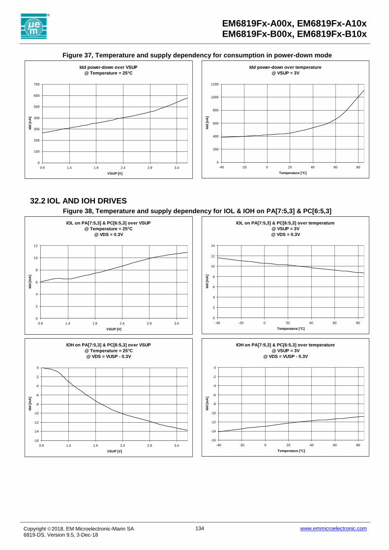
EM6819Fx-A00x, EM6819Fx-A10x EM6819Fx-B00x, EM6819Fx-B10x
Copyright 2018, EM Microelectronic-Marin SA 6819-DS, Version 9.5, 3-Dec-18
134 www.emmicroelectronic.com
Figure 37, Temperature and supply dependency for consumption in power-down mode
Idd power-down over VSUP
@ Temperature = 25°C
0
100
200
300
400
500
600
700
0.9 1.4 1.9 2.4 2.9 3.4
VSUP [V]
Idd
[n
A]
Idd power-down over temperature
@ VSUP = 3V
0
200
400
600
800
1000
1200
-40 -20 0 20 40 60 80
Temperature [°C]
Idd
[n
A]
32.2 IOL AND IOH DRIVES
Figure 38, Temperature and supply dependency for IOL & IOH on PA[7:5,3] & PC[6:5,3]
IOL on PA[7:5,3] & PC[6:5,3] over VSUP
@ Temperature = 25°C
@ VDS = 0.3V
0
2
4
6
8
10
12
0.9 1.4 1.9 2.4 2.9 3.4
VSUP [V]
Idd
[m
A]
IOL on PA[7:5,3] & PC[6:5,3] over temperature
@ VSUP = 3V
@ VDS = 0.3V
0
2
4
6
8
10
12
14
-40 -20 0 20 40 60 80
Temperature [°C]
Idd
[m
A]
IOH on PA[7:5,3] & PC[6:5,3] over VSUP
@ Temperature = 25°C
@ VDS = VUSP - 0.3V
-16
-14
-12
-10
-8
-6
-4
-2
0
0.9 1.4 1.9 2.4 2.9 3.4
VSUP [V]
Idd
[m
A]
IOH on PA[7:5,3] & PC[6:5,3] over temperature
@ VSUP = 3V
@ VDS = VUSP - 0.3V
-16
-14
-12
-10
-8
-6
-4
-2
0
-40 -20 0 20 40 60 80
Temperature [°C]
Idd
[m
A]

EM6819Fx-A00x, EM6819Fx-A10x EM6819Fx-B00x, EM6819Fx-B10x
Copyright 2018, EM Microelectronic-Marin SA 6819-DS, Version 9.5, 3-Dec-18
135 www.emmicroelectronic.com
Figure 39, Temperature and supply dependency for IOL & IOH on PA[4,2:0] & PC[7,4,2:0]
IOL on PA[4,2:0] & PC[7,4,2:0] over VSUP
@ Temperature = 25°C
@ VDS = 0.3V
0
1
2
3
4
5
6
0.9 1.4 1.9 2.4 2.9 3.4
VSUP [V]
Idd
[m
A]
IOL on PA[4,2:0] & PC[7,4,2:0] over temperature
@ VSUP = 3V
@ VDS = 0.3V
0
1
2
3
4
5
6
7
-40 -20 0 20 40 60 80
Temperature [°C]
Idd
[m
A]
IOH on PA[4,2:0] & PC[7,4,2:0] over VSUP
@ Temperature = 25°C
@ VDS = VUSP - 0.3V
-4.5
-4
-3.5
-3
-2.5
-2
-1.5
-1
-0.5
0
0.9 1.4 1.9 2.4 2.9 3.4
VSUP [V]
Idd
[m
A]
IOH on PA[4,2:0] & PC[7,4,2:0] over temperature
@ VSUP = 3V
@ VDS = VUSP - 0.3V
-4.5
-4
-3.5
-3
-2.5
-2
-1.5
-1
-0.5
0
-40 -20 0 20 40 60 80
Temperature [°C]
Idd
[m
A]

EM6819Fx-A00x, EM6819Fx-A10x EM6819Fx-B00x, EM6819Fx-B10x
Copyright 2018, EM Microelectronic-Marin SA 6819-DS, Version 9.5, 3-Dec-18
136 www.emmicroelectronic.com
Figure 40, Temperature and supply dependency for IOL & IOH on PB[7:0]
IOL on PB[7:0] over VSUP
@ Temperature = 25°C
@ VDS = 0.3V
0
2
4
6
8
10
12
0.9 1.4 1.9 2.4 2.9 3.4
VSUP [V]
Idd
[m
A]
IOL on PB[7:0] over temperature
@ VSUP = 3V
@ VDS = 0.3V
0
2
4
6
8
10
12
14
-40 -20 0 20 40 60 80
Temperature [°C]
Idd
[m
A]
IOH on PB[7:0] over VSUP
@ Temperature = 25°C
@ VDS = VUSP - 0.3V
-16
-14
-12
-10
-8
-6
-4
-2
0
0.9 1.4 1.9 2.4 2.9 3.4
VSUP [V]
Idd
[m
A]
IOH on PB[7:0] over temperature
@ VSUP = 3V
@ VDS = VUSP - 0.3V
-16
-14
-12
-10
-8
-6
-4
-2
0
-40 -20 0 20 40 60 80
Temperature [°C]
Idd
[m
A]

EM6819Fx-A00x, EM6819Fx-A10x EM6819Fx-B00x, EM6819Fx-B10x
Copyright 2018, EM Microelectronic-Marin SA 6819-DS, Version 9.5, 3-Dec-18
137 www.emmicroelectronic.com
32.3 PULL-UP AND PULL-DOWN
Figure 41, Temperature and supply dependency for pull-down & pull_up on PA[7:0] & PC[7:0]
Pull-down on PA[7:0] & PC[7:0] over VSUP
@ Temperature = 25°C
70000
71000
72000
73000
74000
75000
76000
77000
78000
79000
80000
0.9 1.4 1.9 2.4 2.9 3.4
VSUP [V]
R [
Oh
m]
Pull-down on PA[7:0] & PC[7:0] over temperature
@ VSUP = 3V
70000
71000
72000
73000
74000
75000
76000
77000
78000
79000
80000
-40 -20 0 20 40 60 80
Temperature [°C]
R [
Oh
m]
Pull-up on PA[7:0] & PC[7:0] over VSUP
@ Temperature = 25°C
70000
71000
72000
73000
74000
75000
76000
77000
78000
79000
80000
0.9 1.4 1.9 2.4 2.9 3.4
VSUP [V]
R [
Oh
m]
Pull-up on PA[7:0] & PC[7:0] over temperature
@ VSUP = 3V
70000
71000
72000
73000
74000
75000
76000
77000
78000
79000
80000
-40 -20 0 20 40 60 80
Temperature [°C]
R [
Oh
m]

EM6819Fx-A00x, EM6819Fx-A10x EM6819Fx-B00x, EM6819Fx-B10x
Copyright 2018, EM Microelectronic-Marin SA 6819-DS, Version 9.5, 3-Dec-18
138 www.emmicroelectronic.com
Figure 42, Temperature and supply dependency for pull-down & pull_up on PB[7:0]
Pull-down on PB[7:0] over VSUP
@ Temperature = 25°C
65000
66000
67000
68000
69000
70000
71000
72000
73000
74000
75000
0.9 1.4 1.9 2.4 2.9 3.4
VSUP [V]
R [
Oh
m]
Pull-down on PB[7:0] over temperature
@ VSUP = 3V
65000
66000
67000
68000
69000
70000
71000
72000
73000
74000
75000
-40 -20 0 20 40 60 80
Temperature [°C]
R [
Oh
m]
Pull-up on PB[7:0] over VSUP
@ Temperature = 25°C
65000
66000
67000
68000
69000
70000
71000
72000
73000
74000
75000
0.9 1.4 1.9 2.4 2.9 3.4
VSUP [V]
R [
Oh
m]
Pull-up on PB[7:0] over temperature
@ VSUP = 3V
65000
66000
67000
68000
69000
70000
71000
72000
73000
74000
75000
-40 -20 0 20 40 60 80
Temperature [°C]
R [
Oh
m]

EM6819Fx-A00x, EM6819Fx-A10x EM6819Fx-B00x, EM6819Fx-B10x
Copyright 2018, EM Microelectronic-Marin SA 6819-DS, Version 9.5, 3-Dec-18
139 www.emmicroelectronic.com
32.4 RC OSCILLATOR 15MHZ AND 2MHZ Figure 43, Temperature and supply dependency for internal RC oscillators
RC 15Mhz frequency error over VSUP
@ Temperature = 25°C
-10
-8
-6
-4
-2
0
2
4
6
8
10
2.2 2.4 2.6 2.8 3 3.2 3.4 3.6
VSUP [V]
Fre
qu
en
cy
err
or
[%]
RC 15Mhz frequency error over temperature
@ VSUP 3V
-10
-8
-6
-4
-2
0
2
4
6
8
10
-40 -20 0 20 40 60 80
Temperature [°C]
Fre
qu
en
cy
err
or
[%]
RC 2Mhz frequency error over VSUP
@ Temperature = 25°C
-10
-8
-6
-4
-2
0
2
4
6
8
10
0.9 1.2 1.5 1.8 2.1 2.4 2.7 3 3.3 3.6
VSUP [V]
Fre
qu
en
cy
err
or
[%]
RC 2Mhz frequency error over temperature
@ VSUP = 3V
-10
-8
-6
-4
-2
0
2
4
6
8
10
-40 -20 0 20 40 60 80
Temperature [°C]
Fre
qu
en
cy
err
or
[%]

EM6819Fx-A00x, EM6819Fx-A10x EM6819Fx-B00x, EM6819Fx-B10x
Copyright 2018, EM Microelectronic-Marin SA 6819-DS, Version 9.5, 3-Dec-18
140 www.emmicroelectronic.com
33. ELECTRICAL SPECIFICATION
33.1 ABSOLUTE MAXIMUM RATINGS Min. Max. Units
Power supply VSUP-VSS - 0.2 +3.8 V
Input voltage VSS – 0.2 VSUP+0.2 V
Storage temperature - 40 + 125 °C
Electrostatic discharge to Mil-Std-883C method 3015.7 with ref. to VSS
-2000 +2000 V
Maximum soldering conditions Packages are Green-Mold and Lead-free
As per Jedec J-STD-020C
Stresses above these listed maximum ratings may cause permanent damage to the device. Exposure beyond specified electrical characteristics may affect device reliability or cause malfunction
33.2 HANDLING PROCEDURES This device has built-in protection against high static voltages or electric fields; however, anti-static precautions should be taken as for any other CMOS integrated circuit. Unless otherwise specified, proper operation can only occur when all terminal voltages are kept within the supply voltage range.
33.3 STANDARD OPERATING CONDITIONS Parameter MIN TYP MAX Unit Description
Temperature -40 25 85 °C
VSUP_range 0.9 3 3.6 V Voltage at power-up
DCDC VSUP min 0.6 V Minimum battery voltage after start-up with DC-DC enabled; maximum current load 10 mA at 0.6V
IVSS max 80 mA Maximum current out of VSS Pin
IVSUP max 80 mA Maximum current into VSUP Pin
DCDC input current
500 mA Maximum current from the Battery into the DCDC
VSS 0 V Reference terminal
CVREG (1) 400 nF regulated voltage capacitor
CVSUP (with dc-dc) 40 uF Supply voltage capacitor with DC-DC
LDCDC (with dc-dc) 39 uH DC-DC coil
Flash data retention
20 yrs Read and Erase state retention
Flash cycling 10k cycle 1 cycle is one erase followed by 1 write
Note 1: This capacitor filters switching noise from VSUP to keep it away from the internal logic and memory cells. In noisy systems the capacitor should be chosen higher than minimum value.

EM6819Fx-A00x, EM6819Fx-A10x EM6819Fx-B00x, EM6819Fx-B10x
Copyright 2018, EM Microelectronic-Marin SA 6819-DS, Version 9.5, 3-Dec-18
141 www.emmicroelectronic.com
33.4 TYPICAL 32KHZ CRYSTAL SPECIFICATION Fq 32768 Hz nominal frequency
Rqs 35 KOhm typical quartz serial resistance
CL 8.2 pF typical quartz load capacitance
df/f 30 ppm quartz frequency tolerance
Watch type crystal oscillator (i.e Microcrystal DS15 ), connected between QIN and Qout terminal.
33.5 TYPICAL 4MHZ CRYSTAL SPECIFICATION FR 4 MHz nominal frequency
RS 22 Ohm Typical equivalent resistor
CS 3.8 pF Typical equivalent serial capacitor
CP 19.8 pF Typical equivalent parallel capacitor
LS 460 uH Typical equivalent inductor
df/f 30 ppm quartz frequency tolerance
33.6 TYPICAL 4MHZ RESONATOR SPECIFICATION FR 4 MHz nominal frequency
RS 9 Ohm Typical equivalent resistor
CS 0.007 pF Typical equivalent serial capacitor
CP 2.39 pF Typical equivalent parallel capacitor
LS 210 mH Typical equivalent inductor
df/f 0.5 % Resonator frequency tolerance
Watch type resonator oscillator CERALOCK Murata CSTLS4M00G53–B0, connected between QIN and Qout terminal.

EM6819Fx-A00x, EM6819Fx-A10x EM6819Fx-B00x, EM6819Fx-B10x
Copyright 2018, EM Microelectronic-Marin SA 6819-DS, Version 9.5, 3-Dec-18
142 www.emmicroelectronic.com
33.7 DC CHARACTERISTICS - POWER SUPPLY CURRENTS Conditions: In active mode, the software makes a loop and writes/reads continuously the RAM, the following blocks are active: NVM instructions read access RAM read/write access Prescalers 1 & 2 Selected oscillator RC 8kHz
Regulator Voltage multiplier in low voltage mode Brown-out Power on reset Internal bias current generation
In stand-by mode, the software execution is stopped; the following blocks are active: Prescalers 1 & 2 Selected oscillator RC 8kHz Regulator
Voltage multiplier in low voltage mode Brown-out Power on reset Internal bias current generation
In sleep mode, the software execution is stopped; the following blocks are active: RC 8kHz Regulator Voltage multiplier in low voltage mode
Brown-out Power on reset Internal bias current generation
In power-down mode, the software execution is stopped; the following blocks are active: Power on reset Internal bias current generation Following table includes product: EM6819FX-AXX0 / -BXX0 / -BXX4 , all measures without DCDC
Parameter Conditions Symbol Min. Typ. Max. Unit
ACTIVE Supply Current CPU on RC=15MHz, no div
VSUP =3V, -40 to 85°C, 7.5 MIPS IVSUPA15MD1 1.05 1.7 mA
ACTIVE Supply Current CPU on RC=2MHz, no div
VSUP =3V, -40 to 85°C, 1 MIPS IVSUPA2MD1 140 250 uA VSUP =1.2V, -40 to 85°C, 1MIPS Note2 IVSUPA2MD1 490 uA
ACTIVE Supply Current CPU on XTal=32KHz, no div
VSUP =3V, -40 to 85°C, 16 kIPS IVSUPA32K 4.2 13 uA VSUP =3V, -40 to 60°C, 16 kIPS IVSUPA32K 4.2 8 uA
ACTIVE Supply Current CPU on RC=8KHz, no div
VSUP =3V, -40 to 85°C, 4 kIPS IVSUPA8K 3.5 uA
Std-by Supply Current Peri on RC=15MHz, no div
VSUP =3V, -40 to 85°C, HF Div=1 IVSUPH15MD1 72 uA
Std-by Supply Current Peri on RC=2MHz, no div
VSUP =3V, -40 to 85°C, HF Div=1 StdByFastWkUp=0
IVSUPH2MD1 14 uA
Std-by Supply Current Peri on RC=2MHz (2), no div
VSUP =1.2V, -40 to 85°C, HF Div=1 IVSUPH2MD1 35 uA
Std-by Supply Current Peri on XTal=32KHz, no div
VSUP =3V, -40 to 85°C, HF RC off StdByFastWkUp=0
IVSUPH32K 2.3 10 uA
VSUP =1.2V, -40 to 85°C, HF RC off StdByFastWkUp=0, Note2 IVSUPH32K 5 uA
VSUP =3V, -40 to 60°C, HF RC off StdByFastWkUp=0
IVSUPH32K 2.3 5 uA
Std-by Supply Current Peri on RC=8KHz, no div
VSUP =3V, -40 to 85°C, HF RC off StdByFastWkUp=0
IVSUPH8K 2.3 9 uA
VSUP =3V, -40 to 60°C, HF RC off StdByFastWkUp=0 IVSUPH8K 2.3 5 uA
Sleep Supply Current Wake-up counter on
VSUP =3V, -40 to 85°C StdByFastWkUp=0
IVSUPSWK 1.95 8 uA
VSUP =3V, -40 to 60°C, RC 8kHz on StdByFastWkUp=0 IVSUPSWK 1.95 4 uA
Sleep Supply Current Wake-up counter off
VSUP =3V, -40 to 85°C, RC8kHz off StdByFastWkUp=0
IVSUPSLEEP 1.9 uA
Powerdown
VSUP =3V, -40 to 25°C IVSUPPWDWN 0.45 0.65 uA VSUP =3V, -40 to 60°C IVSUPPWDWN 0.45 0.8 uA VSUP =3V, -40 to 85°C IVSUPPWDWN 0.45 1.65 uA
Note 2: Internal voltage multiplier enable.

EM6819Fx-A00x, EM6819Fx-A10x EM6819Fx-B00x, EM6819Fx-B10x
Copyright 2018, EM Microelectronic-Marin SA 6819-DS, Version 9.5, 3-Dec-18
143 www.emmicroelectronic.com
Following table includes product: EM6819FX-XX5 / -XX6, all measures without DCDC
Parameter Conditions Symbol Min. Typ. Max. Unit
ACTIVE Supply Current CPU on RC=15MHz, no div
VSUP =3V, -40 to 85°C, 7.5 MIPS IVSUPA15MD1 0.85 1.2 mA
ACTIVE Supply Current CPU on RC=2MHz, no div
VSUP =3V, -40 to 85°C, 1 MIPS IVSUPA2MD1 116 180 uA VSUP =1.2V, -40 to 85°C, 1MIPS Note2 IVSUPA2MD1 490 uA
ACTIVE Supply Current CPU on XTal=32KHz, no div
VSUP =3V, -40 to 85°C, 16 kIPS IVSUPA32K 4.2 13 uA VSUP =3V, -40 to 60°C, 16 kIPS IVSUPA32K 4.2 8 uA
ACTIVE Supply Current CPU on RC=8KHz, no div
VSUP =3V, -40 to 85°C, 4 kIPS IVSUPA8K 3.5 uA
Std-by Supply Current Peri on RC=15MHz, no div
VSUP =3V, -40 to 85°C, HF Div=1 IVSUPH15MD1 72 uA
Std-by Supply Current Peri on RC=2MHz, no div
VSUP =3V, -40 to 85°C, HF Div=1 IVSUPH2MD1 14 uA
Std-by Supply Current Peri on XTal=32KHz, no div
VSUP =3V, -40 to 85°C, HF RC off StdByFastWkUp=0
IVSUPH32K 2.3 10 uA
VSUP =3V, -40 to 60°C, HF RC off StdByFastWkUp=0
IVSUPH32K 2.3 5 uA
Std-by Supply Current Peri on RC=8KHz, no div
VSUP =3V, -40 to 85°C, HF RC off StdByFastWkUp=0
IVSUPH8K 2.3 9 uA
VSUP =3V, -40 to 60°C, HF RC off StdByFastWkUp=0 IVSUPH8K 2.3 5 uA
Sleep Supply Current Wake-up counter on
VSUP =3V, -40 to 85°C StdByFastWkUp=0
IVSUPSWK 1.95 8 uA
VSUP =3V, -40 to 60°C, RC 8kHz on StdByFastWkUp=0 IVSUPSWK 1.95 4 uA
Sleep Supply Current Wake-up counter off
VSUP =3V, -40 to 85°C, RC8kHz off IVSUPSLEEP 1.9 uA
Powerdown Current
VSUP =3V, -40 to 25°C IVSUPPWDWN 0.45 0.65 uA VSUP =3V, -40 to 60°C IVSUPPWDWN 0.45 0.8 uA VSUP =3V, -40 to 85°C IVSUPPWDWN 0.45 1.65 uA
Note 2: Internal voltage multiplier enable.

EM6819Fx-A00x, EM6819Fx-A10x EM6819Fx-B00x, EM6819Fx-B10x
Copyright 2018, EM Microelectronic-Marin SA 6819-DS, Version 9.5, 3-Dec-18
144 www.emmicroelectronic.com
33.8 DC CHARACTERISTICS – VOLTAGE DETECTION LEVELS Parameter Conditions Symbol Min. Typ. Max. Unit
POR VSUP static level on rising edge
-40 to 85°C VPORRIS 0.7 0.86 V
POR VSUP static level on falling edge
-40 to 85°C VPORFAL 0.58 0.74 V
Temperature coefficient -40 to 25°C TVLD_COEF_LO -0.110 0.01 0.134 %/°C
25 to 85°C TVLD_COEF_HI -0.117 0.01 0.142 %/°C
VLD0, VBAT decreasing 25°C VVLD0 0.800 V
VLD1, VBAT decreasing 25°C VVLD1 0.820 V
VLD2, VBAT decreasing 25°C VVLD2 0.840 V
VLD3, VBAT decreasing 25°C VVLD3 0.860 V
VLD4, VBAT decreasing 25°C VVLD4 0.880 V
VLD5, VBAT decreasing 25°C VVLD5 0.900 V
VLD6, VBAT decreasing 25°C VVLD6 0.920 V
VLD7, VBAT decreasing 25°C VVLD7 0.940 V
VLD8, VBAT decreasing 25°C VVLD8 0.960 V
VLD9, VBAT decreasing 25°C VVLD9 0.980 V
VLD10, VBAT decreasing 25°C VVLD10 1.000 V
VLD11, VBAT decreasing 25°C VVLD11 1.100 V
VLD12, VBAT decreasing 25°C VVLD12 1.150 V
VLD13, VBAT decreasing 25°C VVLD13 1.200 V
VLD14, VBAT decreasing 25°C VVLD14 1.300 V
VLD15, VBAT decreasing 25°C VVLD15 1.400 V
VLD16, VBAT decreasing 25°C VVLD16 1.450 V
VLD17, VBAT decreasing 25°C VVLD17 1.500 V
VLD18, VBAT decreasing 25°C VVLD18 1.600 V
VLD19, VBAT decreasing 25°C VVLD19 1.700 V
VLD20, VBAT decreasing 25°C VVLD20 1.900 V
VLD21, VBAT decreasing 25°C VVLD21 2.100 V
VLD22, VBAT decreasing 25°C VVLD22 2.300 V
VLD23, VBAT decreasing 25°C VVLD23 2.400 V
VLD24, VBAT decreasing 25°C VVLD24 2.500 V
VLD25, VBAT decreasing 25°C VVLD25 2.550 V
VLD26, VBAT decreasing 25°C VVLD26 2.600 V
VLD27, VBAT decreasing 25°C VVLD27 2.700 V
VLD28, VBAT decreasing 25°C VVLD28 2.800 V
VLD29, VBAT decreasing 25°C VVLD29 2.900 V
VLD30, VBAT decreasing 25°C VVLD30 2.950 V
VLD31, VBAT decreasing 25°C VVLD31 2.981 3.000 3.025 V
VLD trim bit step / LSB 1.7 mV/V
33.9 DC CHARACTERISTICS – REFERENCE VOLTAGE Parameter Conditions Symbol Min. Typ. Max. Unit
Temperature coefficient -40 to 25°C TBGR_COEF_LO -0.102 0.01 0.128 %/°C
Temperature coefficient 25 to 85°C TBGR_COEF_HI -0.112 0.01 0.136 %/°C
Reference voltage after trimming
VSUP =3V, 25°C VBGP 1.225 1.236 1.247 V
Output load current on PA[2]
VSUP =3V, -40 to 85°C, VBGP output 10 uA

EM6819Fx-A00x, EM6819Fx-A10x EM6819Fx-B00x, EM6819Fx-B10x
Copyright 2018, EM Microelectronic-Marin SA 6819-DS, Version 9.5, 3-Dec-18
145 www.emmicroelectronic.com
33.10 DC CHARACTERISTICS – DC-DC CONVERTER VBAT is input voltage of DC-DC (main Battery), VSUP is output voltage of DC-DC
Parameter Conditions Symbol Min. Typ. Max. Unit
Battery voltage range -40 to 85°C VBAT 0.9 1.8 V
DC-DC level 2.1 -40 to 85°C ; VBATMIN to VBATMAX
VDCDC2.1 2.1 V
DC-DC level 2.5 -40 to 85°C ; VBATMIN to VBATMAX
VDCDC2.5 2.5 V
DC-DC level 2.9 -40 to 85°C ; VBATMIN to VBATMAX
VDCDC2.9 2.9 V
DC-DC level 3.3 -40 to 85°C ; VBATMIN to VBATMAX
VDCDC3.3 3.3 V
Output ripple -40 to 85°C ; VBATMIN to VBATMAX
VRIP +/-100 mV
Max external current current load
-40 to 85°C ; @VBATMIN
ILOAD09V 40 mA
@ VBATMax, VDCDC =3.3V ILOAD18V 150 mA
DC-DC efficiency -40 to 85°C ; VBATMIN to VBATMAX
DCDCEFF 85 %
33.11 DC CHARACTERISTICS – OSCILLATORS Parameter Conditions Symbol Min. Typ. Max. Unit
32KHz XTAL Integrated Input capacitor
Reference on VSS
T=25C CIN 7 pF
32KHz Xtal Integrated Output capacitor
Reference on VSS
T=25C COUT 14 pF
32KHz Xtal Oscillator start time
VSUP > VSUPMin
T=25C tdosc 0.5 4 s
4MHz resonator start time VSUP > VSUPMin
T=25C tdosc 1 10 ms
4MHz XTal start time VSUP > VSUPMin
T=25C tdosc 3 30 ms
RC oscillator 15MHz Temperature coefficient
-40 to 25°C TRC15_COEF_LO -0.018 0.04 0.106 %/°C
RC oscillator 15MHz Temperature coefficient
25 to 85°C TRC15_COEF_HI -0.055 0.004 0.069 %/°C
RC Oscillator 15MHz After trimming, 25°C FRC15M 14.6129 14.7456 14.8783 MHz
RC Oscillator 15MHz
Trimm range 15MHz +50/-30 %
RC Oscillator 15MHz
Trimm step / LSB 47.8 kHz
RC oscillator 2MHz Temperature coefficient
-40 to 25°C TRC2_COEF_LO -0.031 0.08 0.177 %/°C
RC oscillator 2MHz Temperature coefficient
25 to 85°C TRC2_COEF_HI -0.058 0.05 0.164 %/°C
RC Oscillator 2MHz After trimming, 25°C FRC1MHz 1.976 2 2.024 MHz
RC oscillator 2MHz
Trimm range 2MHz +50/-30
%
RC oscillator 2MHz
Trimm step / LSB 8.3 kHz
RC Oscillator 8kHz 6.7 kHz

EM6819Fx-A00x, EM6819Fx-A10x EM6819Fx-B00x, EM6819Fx-B10x
Copyright 2018, EM Microelectronic-Marin SA 6819-DS, Version 9.5, 3-Dec-18
146 www.emmicroelectronic.com
33.12 DC CHARACTERISTICS – VHIGH Parameter Conditions Symbol Min. Typ. Max. Unit
VHIGH level VSUP low VSUP < 1.6V, -40 to 85°C VHighLOW 1.6 2.0 V
VHIGH level VSUP high VSUP > 1.6V, -40 to 85°C
VHighHI VSUP-0.1
VSUP V
33.13 DC CHARACTERISTICS – OPAMP Parameter Conditions Symbol Min. Typ. Max. Unit
Open loop gain VSUP =3V, -40 to 85°C A0 70 dB
Gain band width VSUP =3V, -40 to 85°C GBW 0.7 MHz
Phase margin VSUP =3V, -40 to 85°C PM 60 °
PSRR @ 100kHz VSUP =3V, -40 to 85°C PSRR -24 dB
CMRR @ 100kHz VSUP =3V, -40 to 85°C CMRR -47 dB
Noise VSUP =3V, -40 to 85°C NOISE 10 uV
Input offset VSUP =3V, -40 to 85°C VINOFFSET - +/-10 mV
Reaction time to enable signal
VSUP =3V, -40 to 85°C TON 20 us
Output voltage swing VSUP =3.0V, -40 to 85°C
VINCM=350mV
OPAMP supply Vreg
VOS 1.3 1.85 V
Current load IOH VSUP =3V, -40 to 85°C ILOAD -180 uA
Current load IOL VSUP =3V, -40 to 85°C ILOAD 150 uA
Slew rate VSUP =3.0V, -40 to 85°C
VINCM=350mV SR 0.6 V/us
33.14 DC CHARACTERISTICS – ADC 10 bits ADC considered (RegADCOut1.ADCOutLSB is ignored)
Parameter Conditions Symbol Min. Typ. Max. Unit
ADC offset Temperature coefficient
-40 to 25°C TADC_COEF_LO -0.108 0.01 0.135 %/°C
ADC offset Temperature coefficient
25 to 85°C TADC_COEF_HI -0.114 0.02 0.150 %/°C
ADC offset VSUP =3V, 25°C
ADCref = VBGP ; Rate 91kS/s Range 8/8 ADCOffset -4 0 4 LSB
ADC DNL VSUP =3V, -40 to 85°C
ADCref = VBGP ; Rate 91kS/s ; Range 8/8 ADCDNL -2 0 2 LSB
ADC INL + gain error
VSUP =3V, -40 to 85°C
ADCref = VBGP ; Rate 91kS/s ; Range 8/8 ADCINLT -13 0 13 LSB
ADC INL best fit VSUP =3V, -40 to 85°C
ADCref = VBGP ; Rate 91kS/s ; Range 8/8 ADCINLbestfit -6 0 6 LSB
ADC DNL range 8/8 VSUP =3V, -40 to 85°C
ADCref = VBGP ; Rate 45kS/s ; Range 8/8 ADCDNL6/8 +/- 0.5
LSB
ADC DNL range 6/8 VSUP =3V, -40 to 85°C
ADCref = VBGP ; Rate 45kS/s ; Range 6/8 ADCDNL6/8 +/- 0.5
LSB
ADC DNL range 4/8 VSUP =3V, -40 to 85°C
ADCref = VBGP ; Rate 45kS/s ; Range 4/8 ADCDNL4/8 +/- 0.5
LSB
ADC INL best fit range 6/8
VSUP =3V, -40 to 85°C
ADCref = VBGP ; Rate 45kS/s ; Range 6/8 ADCINLT6/8 +/- 4 LSB
ADC INL best fit range 4/8
VSUP =3V, -40 to 85°C
ADCref = VBGP ; Rate 45kS/s ; Range 4/8 ADCINLT4/8 +/- 4 LSB
ADC INL best fit range 3/8
VSUP =3V, -40 to 85°C
ADCref = VBGP ; Rate 45kS/s ; Range 3/8 ADCINLT4/8 +/- 4 LSB

EM6819Fx-A00x, EM6819Fx-A10x EM6819Fx-B00x, EM6819Fx-B10x
Copyright 2018, EM Microelectronic-Marin SA 6819-DS, Version 9.5, 3-Dec-18
147 www.emmicroelectronic.com
33.15 DC CHARACTERISTICS – TEMPERATURE SENSOR 10 bits ADC considered (RegADCOut1.ADCOutLSB is ignored)
Parameter Conditions Symbol Min. Typ. Max. Unit
Temp sensor result at 25° VSUP =3V Tempsens25 416 LSB
Temp sensor result at -40° VSUP =3V Tempsens-40 183 LSB
Temp sensor result at 60° VSUP =3V Tempsens60 550 LSB
Temp sensor result at 85° VSUP =3V Tempsens85 639 LSB
Temp sensor slope VSUP =3V ; Temp range 0° - 60° Tempsensslope 3.8 LSB/°
Temp sensor linearity VSUP =3V ; Temp range 0° - 60° Tempsenslin +/-0.8 %
Note: offset & calibration values stored in NVM are coded on 11bits than values are twice values in above table.
33.16 DC CHARACTERISTICS - I/O PINS (ON PACKAGE) Conditions: T= -40 to 85C, VSUP=3.0V (unless otherwise specified) Parameter Conditions Symbol Min. Typ. Max. Unit
Input Low voltage
Ports A,B, C VIL VSS 0.2* VSUP
V
Input High voltage
Ports A,B, C VIH 0.8* VSUP
VSUP V
Input Hysteresis PA[7:0], PB[7:0], PC[7:0]
Temp=25°C VHyst 0.42 V
IOL (high current drives) PA[7:5,3], PB[7:0], PC[6:5,3]
VSUP =3.0V , VOL=0.3V IOL 4.2 9.9 mA
VSUP =3.0V , VOL=0.6V IOL 19.8 mA
VSUP =3.0V , VOL=1.0V IOL 33.0 mA
IOL PA[4,2:0], PC[7,4,2:0]
VSUP =3.0V , VOL=0.3V IOL 1.6 5.2 mA
VSUP =3.0V , VOL=0.6V IOL 10.4 mA
VSUP =3.0V , VOL=1.0V IOL 17.3 mA
IOH (high current drives) PA[7:5,3], PB[7:0], PC[6:5,3]
VSUP =3.0V , VOH= VSUP - 0.3V IOH -12.7 -6.5 mA
VSUP =3.0V , VOH= VSUP - 0.6V IOH -25.4 mA
VSUP =3.0V , VOH= VSUP - 1.0V IOH -42.3 mA
VOH (high current drives) PA[3], PA[6], PB[6], PB[7]
VSUP=3.3V, IOH= -20mA VOH VSUP-0.82
VSUP-0.6
VSUP V
IOH PA[4,2:0], PC[7,4,2:0]
VSUP =3.0V , VOH= VSUP - 0.3V IOH -3.3 -1.0 mA
VSUP =3.0V , VOH= VSUP - 0.6V IOH -6.6 mA
VSUP =3.0V , VOH= VSUP - 1.0V IOH -11.0 mA
Input Pull-down Port A,B,C
VSUP =3.0V, Pin at 3.0V RPD 35k 70k 100k Ohm
Input Pull-up Port A,B,C
VSUP =3.0V, Pin at 0.0V
RPU
35k 70k 100k Ohm
Input Pull-down TM
VSUP =3.0V, Pin at 3.0V RPDTM 20k Ohm

EM6819Fx-A00x, EM6819Fx-A10x EM6819Fx-B00x, EM6819Fx-B10x
Copyright 2018, EM Microelectronic-Marin SA 6819-DS, Version 9.5, 3-Dec-18
148 www.emmicroelectronic.com
33.17 DC CHARACTERISTICS - I/O PINS (ON DIE)
Conditions: T= -40 to 85C, VSUP=3.0V (unless otherwise specified) Parameter Conditions Symbol Min. Typ. Max. Unit
Input Low voltage
Ports A,B, C VIL VSS 0.2* VSUP
V
Input High voltage
Ports A,B, C VIH 0.8* VSUP
VSUP V
Input Hysteresis PA[7:0], PB[7:0], PC[7:0]
Temp=25°C VHyst 0.42 V
IOL (high current drives) PA[7:5,3], PB[7:0], PC[6:5,3]
VSUP =3.0V , VOL=0.3V IOL 3.57 9.9 mA
VSUP =3.0V , VOL=0.6V IOL 19.8 mA
VSUP =3.0V , VOL=1.0V IOL 33.0 mA
IOL PA[4,2:0], PC[7,4,2:0]
VSUP =3.0V , VOL=0.3V IOL 1.36 5.2 mA
VSUP =3.0V , VOL=0.6V IOL 10.4 mA
VSUP =3.0V , VOL=1.0V IOL 17.3 mA
IOH (high current drives) PA[7:5,3], PB[7:0], PC[6:5,3]
VSUP =3.0V , VOH= VSUP - 0.3V IOH -12.7 -5.52 mA
VSUP =3.0V , VOH= VSUP - 0.6V IOH -25.4 mA
VSUP =3.0V , VOH= VSUP - 1.0V IOH -42.3 mA
VOH (high current drives) PA[3], PA[6], PB[6], PB[7]
VSUP=3.3V, IOH= -20mA VOH VSUP-0.82
VSUP-0.6
VSUP V
IOH PA[4,2:0], PC[7,4,2:0]
VSUP =3.0V , VOH= VSUP - 0.3V IOH -3.3 -0.85 mA
VSUP =3.0V , VOH= VSUP - 0.6V IOH -6.6 mA
VSUP =3.0V , VOH= VSUP - 1.0V IOH -11.0 mA
Input Pull-down Port A,B,C
VSUP =3.0V, Pin at 3.0V RPD 35k 70k 100k Ohm
Input Pull-up Port A,B,C
VSUP =3.0V, Pin at 0.0V
RPU
35k 70k 100k Ohm
Input Pull-down TM
VSUP =3.0V, Pin at 3.0V RPDTM 20k Ohm
EM6819Fx-A00x, EM6819Fx-A10x EM6819Fx-B00x, EM6819Fx-B10x
Copyright 2018, EM Microelectronic-Marin SA 6819-DS, Version 9.5, 3-Dec-18
149 www.emmicroelectronic.com
34. WAKEUP AND BOOT SEQUENCE TIMING
Wakeup timing from stand-by mode: Refer to paragraph 2.2.1 Standby mode
Wakeup timing from sleep mode: Refer to paragraph 2.2.3 Sleep Wake-up
Wakeup timing from power-done mode. Refer to paragraph 2.2.4 Power-down mode
Boot sequence timing from power-on-reset: Refer to paragraph 6.1 Boot sequence

EM6819Fx-A00x, EM6819Fx-A10x EM6819Fx-B00x, EM6819Fx-B10x
Copyright 2018, EM Microelectronic-Marin SA 6819-DS, Version 9.5, 3-Dec-18
150 www.emmicroelectronic.com
35. PACKAGE DRAWINGS
35.1 DIMENSIONS OF TSSOP28 PACKAGE
D
A
e
C
A1
N
A2
END VIEW
TOP VIEW
SEATINGPLANE
123
SEEDETAIL "A"
CL
E1
E
b
( )
(VIEW ROTATED 90° C.W.)
DETAIL 'A'
0.25
L
BB
(14°)
(14°)
(1.00)
CCO
0°
0.85
0.19
0.50
4.30
0.09
0.19
OCC
eE
L
b1
2A
b
c
D
E1
6.40 BSC
0.65 BSC
0.60
8°0.70
9.70 BSC
0.22
4.40
-
-
0.90 0.95
0.25
4.50
0.30
0.20
0.05
MIN.
MY
B
O
S
L
A
A1
DIMENSIONSin MILLIMETERS
NOM.1.10
0.15
MAX.
TSSOP28

EM6819Fx-A00x, EM6819Fx-A10x EM6819Fx-B00x, EM6819Fx-B10x
Copyright 2018, EM Microelectronic-Marin SA 6819-DS, Version 9.5, 3-Dec-18
151 www.emmicroelectronic.com
35.2 DIMENSIONS OF TSSOP24 PACKAGE
D
A
e
C
A1
N
A2
END VIEW
TOP VIEW
SEATINGPLANE
123
SEEDETAIL "A"
CL
E1
E
b
( )
(VIEW ROTATED 90° C.W.)
DETAIL 'A'
0.25
L
BB
(14°)
(14°)
(1.00)
CCO
0°
0.85
0.19
0.50
4.30
0.09
0.19
OCC
eE
L
b1
2A
b
c
D
E1
6.40 BSC
0.65 BSC
0.60
8°0.70
7.80 BSC
0.22
4.40
-
-
0.90 0.95
0.25
4.50
0.30
0.20
0.05
MIN.
MY
B
O
S
L
A
A1
DIMENSIONSin MILLIMETERS
NOM.1.10
0.15
MAX.
TSSOP24 (0.65mm pitch, 4.4mm body width)
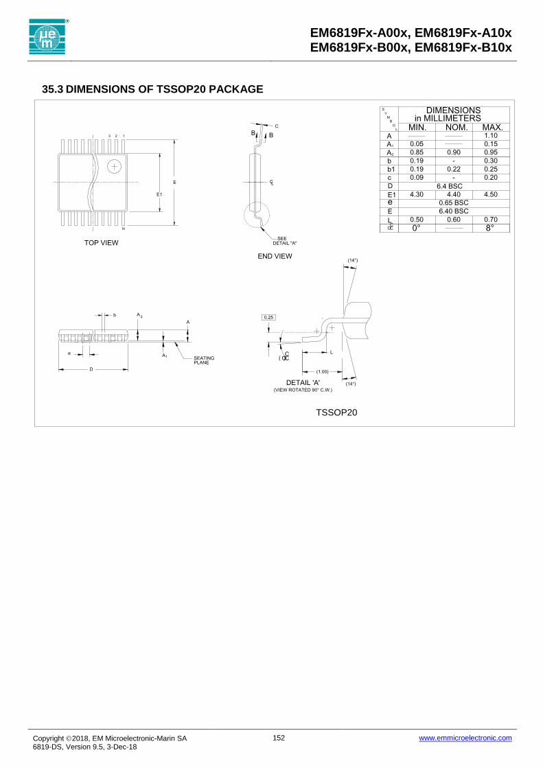
EM6819Fx-A00x, EM6819Fx-A10x EM6819Fx-B00x, EM6819Fx-B10x
Copyright 2018, EM Microelectronic-Marin SA 6819-DS, Version 9.5, 3-Dec-18
152 www.emmicroelectronic.com
35.3 DIMENSIONS OF TSSOP20 PACKAGE
D
A
e
C
A1
N
A2
END VIEW
TOP VIEW
SEATINGPLANE
123
SEEDETAIL "A"
CL
E1
E
b
( )
(VIEW ROTATED 90° C.W.)
DETAIL 'A'
0.25
L
BB
(14°)
(14°)
(1.00)
CCO
0°
0.85
0.19
0.50
4.30
0.09
0.19
OCC
eE
L
b1
2A
b
c
D
E1
6.40 BSC
0.65 BSC
0.60
8°0.70
6.4 BSC
0.22
4.40
-
-
0.90 0.95
0.25
4.50
0.30
0.20
0.05
MIN.
MY
B
O
S
L
A
A1
DIMENSIONSin MILLIMETERS
NOM.1.10
0.15
MAX.
TSSOP20

EM6819Fx-A00x, EM6819Fx-A10x EM6819Fx-B00x, EM6819Fx-B10x
Copyright 2018, EM Microelectronic-Marin SA 6819-DS, Version 9.5, 3-Dec-18
153 www.emmicroelectronic.com
35.4 DIMENSIONS OF TSSOP16 PACKAGE
D
A
e
C
A1
N
A2
END VIEW
TOP VIEW
SEATINGPLANE
123
SEEDETAIL "A"
CL
E1
E
b
( )
(VIEW ROTATED 90° C.W.)
DETAIL 'A'
0.25
L
BB
(14°)
(14°)
(1.00)
CCO
0°
0.85
0.19
0.50
4.30
0.09
0.19
OCC
eE
L
b1
2A
b
c
D
E1
6.40 BSC
0.65 BSC
0.60
8°0.70
5.00 BSC
0.22
4.40
-
-
0.90 0.95
0.25
4.50
0.30
0.20
0.05
MIN.
MY
B
O
S
L
A
A1
DIMENSIONSin MILLIMETERS
NOM.1.10
0.15
MAX.
TSSOP16 (0.65mm pitch, 4.4mm body width)

EM6819Fx-A00x, EM6819Fx-A10x EM6819Fx-B00x, EM6819Fx-B10x
Copyright 2018, EM Microelectronic-Marin SA 6819-DS, Version 9.5, 3-Dec-18
154 www.emmicroelectronic.com
35.5 DIMENSIONS OF SO8 PACKAGE
C
PARTING LINE
SIDE VIEW
D
e
L
DETAIL A
CCO
SEE DETAIL A
1A
B
A
SEATING PLANE
2A
END VIEW
E
TOP VIEW
3
N
H
2 1
0°
0.41
5.84
3.81
0.35
0.1271.55MIN.
0.19
1.40
C
L
CO
1
N
H
eEDCB
AA
OL
YMB
S
A2
8°
0.89
6.20
3.99
0.200.49
0.251.73
COMMONDIMENSIONS
MAX.
1.27 BSC
8
NOM.1.630.15
0.41
3.94
5.99
0.64
5°
0.25
1.47 1.55
THIS TABLE IN MILLIMETERS
4.80 4.93 4.98
SO8 - 150

EM6819Fx-A00x, EM6819Fx-A10x EM6819Fx-B00x, EM6819Fx-B10x
Copyright 2018, EM Microelectronic-Marin SA 6819-DS, Version 9.5, 3-Dec-18
155 www.emmicroelectronic.com
35.6 DIMENSIONS OF QFN32 PACKAGE
0.50 DIA.
TOP VIEW
EE1
E1/2
D1/2
N
D1
D/2
D
E/2
SIDE VIEW
A
A1
A3
PLANE
A2
BOTTOM VIEW
(MIN. 0.35)
L
0.45
D2/2
D2
E2
E2/2
N
b
PIN#1 ID
e (MIN. 0.35)
4.75
3.50
0.40
0.23
E1
3.40
0.30
0.18
D2
L
b
3.60
0.50
0.30
0.50
NOM.MIN.
e
5.0
5.0
E
D
K
A3
A 0.80
0.20min
0.20
0.85 0.90
A2 0.65
ALL DIMENSIONS ARE IN MILLIMETERS
A1 0.00 0.01 0.05
0.60 0.70
3.503.40E2 3.60
MAX.
D1 4.75

EM6819Fx-A00x, EM6819Fx-A10x EM6819Fx-B00x, EM6819Fx-B10x
Copyright 2018, EM Microelectronic-Marin SA 6819-DS, Version 9.5, 3-Dec-18
156 www.emmicroelectronic.com
35.7 DIMENSIONS OF QFN20 PACKAGE
TERMINAL/SIDE
TERMINAL TIP
L
e
L1
BOTTOM VIEW
SEE DETAIL "A
SEE DETAIL "A"
D2
D2/2
K
L
E2
E2/2
K
4 * e
b
2
1
e
4 * e
PIN #1 ID
TOP VIEW
E
D
SIDE VIEWA1
A
A3
2.60
2.60
0.50
0.25
2.50E2
2.50
0.45
0.18
D2
L
b
2.70
2.70
0.55
0.30
0.50
NOM.MIN.
e
MAX.
4.0
4.0
E
D
K
A3
A 0.80
0.20min
0.20
0.85 0.90
L1 0.15max
ALL DIMENSIONS ARE IN MILLIMETERS
A1 0.00 0.02 0.05
DETAIL "A"
PIN #1 ID

EM6819Fx-A00x, EM6819Fx-A10x EM6819Fx-B00x, EM6819Fx-B10x
Copyright 2018, EM Microelectronic-Marin SA 6819-DS, Version 9.5, 3-Dec-18
157 www.emmicroelectronic.com
35.8 PAD LOCATION OF THE DIE (VERSION 005 AND 006)

EM6819Fx-A00x, EM6819Fx-A10x EM6819Fx-B00x, EM6819Fx-B10x
Copyright 2018, EM Microelectronic-Marin SA 6819-DS, Version 9.5, 3-Dec-18
158 www.emmicroelectronic.com
35.9 PAD LOCATION OF THE DIE (ALL OTHER VERSIONS)
Notes: The drawn box is not the real sealring

EM6819Fx-A00x, EM6819Fx-A10x EM6819Fx-B00x, EM6819Fx-B10x
Copyright 2018, EM Microelectronic-Marin SA 6819-DS, Version 9.5, 3-Dec-18
159 www.emmicroelectronic.com
36. PACKAGE MARKING The first line of the package marking contains the Revision ID and the bonding option The remaining lines contain Lot identification information First Line: EM6819 XY wheras XY= Circuit hardware information and package pinout Current Package markings
EM6819 EA (hardware E with DCDC available) EM6819 EB (hardware E without DCDC)
For changes refer to the Errata section.
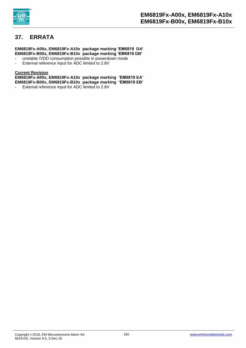
EM6819Fx-A00x, EM6819Fx-A10x EM6819Fx-B00x, EM6819Fx-B10x
Copyright 2018, EM Microelectronic-Marin SA 6819-DS, Version 9.5, 3-Dec-18
160 www.emmicroelectronic.com
37. ERRATA EM6819Fx-A00x, EM6819Fx-A10x package marking ‘EM6819 DA’ EM6819Fx-B00x, EM6819Fx-B10x package marking ‘EM6819 DB’ - unstable IVDD consumption possible in powerdown mode - External reference input for ADC limited to 2.8V Current Revision EM6819Fx-A00x, EM6819Fx-A10x package marking ‘EM6819 EA’ EM6819Fx-B00x, EM6819Fx-B10x package marking ‘EM6819 EB’ - External reference input for ADC limited to 2.8V

EM6819Fx-A00x, EM6819Fx-A10x EM6819Fx-B00x, EM6819Fx-B10x
Copyright 2018, EM Microelectronic-Marin SA 6819-DS, Version 9.5, 3-Dec-18
161 www.emmicroelectronic.com
38. ORDERING INFORMATION The full ordering information is composed out of the - Part number - The package type and pin count for given part number (to be found in table EM6819 family on page 11) - The delivery form (Stick, Tape, Tray) depending on the selected package Examples: - EM6819F6-B100-TP028BD - EM6819F4-A000-LF020D - EM6819F4-A000-WS11
Part Number Refer to table EM6819 family on page 11 for the different part numbers I.e EM6819F6-A000 Package Type and package pin count Refer to table EM6819 family on page 11 for available packages for a given part number. Packages: QFN, TSSOP, SO Pincounts: 8, 16, 20, 28, 32 Package and pincount codes: QFN: LF032 LF020 TSSOP: TP028 TP020 TP016 SO: SO008 Wafer: WS11 Delivery Form The delivery form depends on the selected package type For TSSOP, SO packages - BD Tape and Real For QFN packages - D Tray For wafer The wafer delivery is on sawn wafer backlap at 11 mils. Other die/wafer form delivery Other delivery in die or wafer form is also possible. Please contact EM Microelectronic directly if such delivery is requested. EM Microelectronic-Marin SA (“EM”) makes no warranties for the use of EM products, other than those expressly contained in EM's applicable General Terms of Sale, located at http://www.emmicroelectronic.com. EM assumes no responsibility for any errors which may have crept into this document, reserves the right to change devices or specifications detailed herein at any time without notice, and does not make any commitment to update the information contained herein. No licenses to patents or other intellectual property rights of EM are granted in connection with the sale of EM products, neither expressly nor implicitly. In respect of the intended use of EM products by customer, customer is solely responsible for observing existing patents and other intellectual property rights of third parties and for obtaining, as the case may be, the necessary licenses. Important note: The use of EM products as components in medical devices and/or medical applications, including but not limited to, safety and life supporting systems, where malfunction of such EM products might result in damage to and/or injury or death of persons is expressly prohibited, as EM products are neither destined nor qualified for use as components in such medical devices and/or medical applications. The prohibited use of EM products in such medical devices and/or medical applications is exclusively at the risk of the customer