interconnect planning for physical design of 3d integrated
TRANSCRIPT
Johann Knechtel
Interconnect Planning for Physical Design of3D Integrated Circuits
TU Dresden, December 2013

Technische Universität Dresden
Interconnect Planning for Physical Design of
3D Integrated Circuits
Johann Knechtel
von der Fakultät Elektrotechnik und Informationstechnik der Technischen
Universität Dresden
zur Erlangung des akademischen Grades eines
Doktor-Ingenieurs
(Dr.-Ing.)
genehmigte Dissertation
Vorsitzender: Prof. Dr.-Ing. habil. Dr. h. c. Klaus-Jürgen Wolter
Gutachter: Prof. Dr.-Ing. habil. Jens Lienig, Prof. Dr.-Ing. Günter Elst
Tag der Einreichung: 06.01.2014
Tag der Verteidigung: 14.03.2014

The reward of a thing well done, is to have done it.
Ralph Waldo Emerson, Essays: Second Series (1844)
Acknowledgments
This dissertation concludes a memorable part of my research work during the past three
to four years, and I am very grateful for this experience.
I sincerely thank my advisor, Professor Jens Lienig, for the opportunities he provided
me with, his thoughtful and effective mentoring, the freedom he granted me, and the kind
atmosphere and company, not only regarding work. He paved the way for my research from
the beginning on; he awoke my interest for chip design and its automation in particular.
Without hesitation, he arranged (in the end of 2009) a research visit at the University of
Michigan, USA. Later on, he also helped me to finance another research visit in Hong Kong.
I will keep both—very fruitful—visits in good memory, and appreciate Jens’ support. I am
also thankful to Jens for his encouragement to look into the field of design automation for
3D integration; I believe that this was/is a rewarding path to follow.
Another import person for this dissertation and my academic experience is Professor Igor
L. Markov (University of Michigan). I do thank Igor deeply for his efforts and continuous
support, which he put up during my six-months visit in 2010 and beyond. Igor provided
me with so many valuable insights, ideas and knowledge when it comes to research,
especially in the field of design automation. He also showed me by example that (only)
continuous efforts are leading to reasonable, satisfying results. Furthermore, I want to
thank Igor honestly for the lessons he thought me in technical writing. This learning process
is certainly never-ending, but I have no doubts that I would have struggled much more
without Igor’s help.
Spending the summer 2012 at the Chinese University of Hong Kong, under the guidance
of Professor Evangeline F. Y. Young, was another worthwhile and great experience. I am
grateful to Evangeline for hosting me at her lab, a both thriving and friendly place. The
discussions and collaboration with Evangeline were a notable enrichment for my work; I
appreciate in particular her input on layout representations.
III

Acknowledgments
Besides Jens, Igor and Evangeline, I sincerely thank everyone else who contributed—in
her/his own way—to my research projects and this dissertation. Jin Hu was kind enough
to comment my writing and research ideas whenever asked for. Robert Fischbach and
I shared the same research interest; I enjoyed a great time with him, driven by many
interesting collaborations. I appreciate very much Matthias Thiele’s efforts he put into
our finite-elements analysis for thermal investigations of 3D ICs. Timm Amstein’s work
on optimizing the parametrization for our thermal analysis was a great help. Timm was
always thinking ahead and thus contributing in an efficient manner. Puskar Budhathoki’s
research internship at TU Dresden was quite fruitful; he was able to provide interesting
findings on thermal management of 3D ICs. Jennifer Gaugler, Prof. Jens Lienig, and my
brother Martin provided valuable feedback for editing parts of this dissertation.
I thank the members of the dissertation committee for their efforts and support, espe-
cially Prof. Jens Lienig and Prof. Günter Elst for reading and assessing the dissertation so
promptly.
I thank the German Research Foundation / DFG for funding my research studies. In
this context, the kind support of Bärbel Knöfel was greatly appreciated; she was always
helpful when I had to carry out organizational tasks and cope with paperwork.
I am also very grateful to have met a lot of interesting fellows and friends during my
research time. This includes (but is not limited to) the members of the EECS Department,
University of Michigan; the colleagues at the Institute of Electromechanical and Electronic
Design, TU Dresden; the colleagues at the Research Training Group Nano- and Biotech-
nologies for Packaging of Electronic Systems, TU Dresden; and the students at the CSE
Department, Chinese University of Hong Kong.
Special thanks go to my brother Martin; he was always a role model in recent years,
and a tower of strength at younger ages. Our parents Bernd and Marita have—both in
their own ways—enabled me/us to reach that far, and I acknowledge their support very
much. Finally, I am lucky and thankful to have met my wonderful fiancée Anja during our
time of doctoral studies at TU Dresden—I know that this truly is a great fortune, going far
beyond research achievements.
IV

Contents
Abstract VIII
Kurzfassung IX
1 Introduction 1
1.1 The 3D Integration Approach for Electronic Circuits . . . . . . . . . . . . . . 1
1.2 Technologies for 3D Integrated Circuits . . . . . . . . . . . . . . . . . . . . . 6
1.3 Design Approaches for 3D Integrated Circuits . . . . . . . . . . . . . . . . . . 8
2 State of the Art in Design Automation for 3D Integrated Circuits 13
2.1 Thermal Management . . . . . . . . . . . . . . . . . . . . . . . . . . . . . . . . 13
2.2 Partitioning and Floorplanning . . . . . . . . . . . . . . . . . . . . . . . . . . . 14
2.3 Placement and Routing . . . . . . . . . . . . . . . . . . . . . . . . . . . . . . . 15
2.4 Power and Clock Delivery . . . . . . . . . . . . . . . . . . . . . . . . . . . . . . 16
2.5 Design Challenges . . . . . . . . . . . . . . . . . . . . . . . . . . . . . . . . . . 16
3 Research Objectives 18
4 Planning Through-Silicon Via Islands for Block-Level Design Reuse 21
4.1 Problems for Design Reuse in 3D Integrated Circuits . . . . . . . . . . . . . 21
4.2 Connecting Blocks Using Through-Silicon Via Islands . . . . . . . . . . . . . 23
4.2.1 Problem Formulation and Methodology Overview . . . . . . . . . . 25
4.2.2 Net Clustering . . . . . . . . . . . . . . . . . . . . . . . . . . . . . . . . 26
4.2.3 Insertion of Through-Silicon Via Islands . . . . . . . . . . . . . . . . 31
4.2.4 Deadspace Insertion and Redistribution . . . . . . . . . . . . . . . . . 34
4.3 Experimental Investigation . . . . . . . . . . . . . . . . . . . . . . . . . . . . . 38
4.3.1 Wirelength Estimation . . . . . . . . . . . . . . . . . . . . . . . . . . . 38
V

Contents
4.3.2 Configuration . . . . . . . . . . . . . . . . . . . . . . . . . . . . . . . . . 39
4.3.3 Results and Discussion . . . . . . . . . . . . . . . . . . . . . . . . . . . 41
4.4 Summary and Conclusions . . . . . . . . . . . . . . . . . . . . . . . . . . . . . 46
5 Planning Through-Silicon Vias for Design Optimization 47
5.1 Deadspace Requirements for Optimized Planning of Through-Silicon Vias 48
5.2 Multiobjective Design Optimization of 3D Integrated Circuits . . . . . . . . 50
5.2.1 Methodology Overview and Configuration . . . . . . . . . . . . . . . 50
5.2.2 Techniques for Deadspace Optimization . . . . . . . . . . . . . . . . 51
5.2.3 Design-Quality Analysis . . . . . . . . . . . . . . . . . . . . . . . . . . 55
5.2.4 Planning Different Types of Through-Silicon Vias . . . . . . . . . . . 55
5.3 Experimental Investigation . . . . . . . . . . . . . . . . . . . . . . . . . . . . . 61
5.3.1 Configuration . . . . . . . . . . . . . . . . . . . . . . . . . . . . . . . . . 61
5.3.2 Results and Discussion . . . . . . . . . . . . . . . . . . . . . . . . . . . 65
5.4 Summary and Conclusions . . . . . . . . . . . . . . . . . . . . . . . . . . . . . 70
6 3D Floorplanning for Structural Planning of Massive Interconnects 71
6.1 Block Alignment for Interconnects Planning in 3D Integrated Circuits . . . 72
6.2 Corner Block List Extended for Block Alignment . . . . . . . . . . . . . . . . 74
6.2.1 Alignment Encoding . . . . . . . . . . . . . . . . . . . . . . . . . . . . . 75
6.2.2 Layout Generation: Block Placement and Alignment . . . . . . . . . 78
6.3 3D Floorplanning Methodology . . . . . . . . . . . . . . . . . . . . . . . . . . 85
6.3.1 Optimization Criteria and Phases and Related Cost Models . . . . . 85
6.3.2 Fast Thermal Analysis . . . . . . . . . . . . . . . . . . . . . . . . . . . . 88
6.3.3 Layout Operations . . . . . . . . . . . . . . . . . . . . . . . . . . . . . . 90
6.3.4 Adaptive Optimization Schedule . . . . . . . . . . . . . . . . . . . . . 91
6.4 Experimental Investigation . . . . . . . . . . . . . . . . . . . . . . . . . . . . . 92
6.4.1 Configuration . . . . . . . . . . . . . . . . . . . . . . . . . . . . . . . . . 93
6.4.2 Results and Discussion . . . . . . . . . . . . . . . . . . . . . . . . . . . 94
6.5 Summary and Conclusions . . . . . . . . . . . . . . . . . . . . . . . . . . . . . 99
7 Research Summary, Conclusions, and Outlook 101
Dissertation Theses 107
VI

Contents
Notation 110
Glossary 116
Bibliography 122
VII
Abstract
Vertical stacking—based on modern manufacturing and integration technologies—of mul-
tiple 2D chips enables three-dimensional integrated circuits (3D ICs). This exploitation of
the third dimension is generally accepted for aiming at higher packing densities, hetero-
geneous integration, shorter interconnects, reduced power consumption, increased data
bandwidth, and realizing highly-parallel systems in one device. However, the commer-
cial acceptance of 3D ICs is currently behind its expectations, mainly due to challenges
regarding manufacturing and integration technologies as well as design automation.
This work addresses three selected, practically relevant design challenges: (i) increasing
the constrained reusability of proven, reliable 2D intellectual property blocks, (ii) planning
different types of (comparatively large) through-silicon vias with focus on their impact
on design quality, as well as (iii) structural planning of massively-parallel, 3D-IC-specific
interconnect structures during 3D floorplanning.
A key concept of this work is to account for interconnect structures and their properties
during early design phases in order to support effective and high-quality 3D-IC-design flows.
To tackle the above listed challenges, modular design-flow extensions and methodologies
have been developed. Experimental investigations reveal the effectiveness and efficiency
of the proposed techniques, and provide findings on 3D integration with particular focus
on interconnect structures. We suggest consideration of these findings when formulating
guidelines for successful 3D-IC design automation.
VIII
Kurzfassung
Dreidimensional integrierte Schaltkreise (3D-ICs) beruhen auf neuartigen Herstellungs-
und Integrationstechnologien, wobei vor allem “klassische” 2D-ICs vertikal zu einem neuar-
tigen 3D-System gestapelt werden. Dieser Ansatz zur Erschließung der dritten Dimension
im Schaltkreisentwurf ist nach Expertenmeinung dazu geeignet, höhere Integrationsdich-
ten zu erreichen, heterogene Integration zu realisieren, kürzere Verdrahtungswege zu
ermöglichen, Leistungsaufnahmen zu reduzieren, Datenübertragungsraten zu erhöhen,
sowie hoch-parallele Systeme in einer Baugruppe umzusetzen. Aufgrund von technologi-
schen und entwurfsmethodischen Schwierigkeiten bleibt jedoch bisher die kommerzielle
Anwendung von 3D-ICs deutlich hinter den Erwartungen zurück.
In dieser Arbeit werden drei ausgewählte, praktisch relevante Problemstellungen der
Entwurfsautomatisierung von 3D-ICs bearbeitet: (i) die Verbesserung der (eingeschränk-
ten) Wiederverwendbarkeit von zuverlässigen 2D-Intellectual-Property-Blöcken, (ii) die
komplexe Planung von verschiedenartigen, verhältnismäßig großen Through-Silicion Vias
unter Beachtung ihres Einflusses auf die Entwurfsqualität, und (iii) die strukturelle Ein-
bindung von massiv-parallelen, 3D-IC-spezifischen Verbindungsstrukturen während der
Floorplanning-Phase.
Das Ziel dieser Arbeit besteht darin, Verbindungsstrukturen mit deren wesentlichen
Eigenschaften bereits in den frühen Phasen des Entwurfsprozesses zu berücksichtigen.
Dies begünstigt einen qualitativ hochwertigen Entwurf von 3D-ICs. Die in dieser Arbeit
vorgestellten modularen Entwurfsprozess-Erweiterungen bzw. -Methodiken dienen zur ef-
fizienten Lösung der oben genannten Problemstellungen. Experimentelle Untersuchungen
bestätigen die Wirksamkeit sowie die Effektivität der erarbeiten Methoden. Darüber hinaus
liefern sie praktische Erkenntnisse bezüglich der Anwendung von 3D-ICs und der Planung
deren Verbindungsstrukturen. Diese Erkenntnisse sind zur Ableitung von Richtlinien für
den erfolgreichen Entwurf von 3D-ICs dienlich.
IX
Chapter 1
Introduction
Integrated circuits (ICs) are tied to our daily life in a pervasive manner. All the electronic
devices we use almost constantly nowadays—either directly like our mobile phones and
computers or indirectly like the internet’s infrastructure—are equipped with ICs. The
further we embed electronic devices into our lives, the more sophisticated and functionally
diverse we want them to be. Considering the limitations of manufacturing processes for
complementary metal-oxide-semiconductor (CMOS) microelectronics, which can be quite
complex and cost-intensive to overcome, new paradigms have to eventually be followed.
In this time of transition, the microelectronics industry and researchers in related fields
have taken a leading role in exploring options for modern and future electronic devices.
1.1 The 3D Integration Approach for Electronic Circuits
One important, recently acknowledged trend—in addition to the “classical” down-scaling
of microelectronic nodes—is to aim for more diversification, also coined as More than
Moore (Figure 1.1). In this context, and also to achieve increased packing density and
shorter interconnects, the concept of three-dimensional (3D) integration has emerged.
The key idea of 3D integration for electronic circuits is to vertically stack several
chips/dies, interconnect them, and thus to obtain a “multi-story” device (Figure 1.2). As
with the concept of skyscrapers (vs. low-rise buildings) where a huge amount of people can
wander around in short paths and thus collaborate efficiently, 3D integration of electronic
circuits (vs. classical 2D chips) enables tight and efficient coupling of many functional
modules within one device.
1
Chapter 1. Introduction
Diversification:"More than Moore"
Scaling:"More Moore" Sensors,
ActuatorsAnalog, RF,
MemoryBiochipsPhotonics
130 nm
90 nm
65 nm
45 nm
32 nm
22 nm
...
StandardCMOS
Performance
Functionality
3D IntegratedCircuits
BeyondCMOS
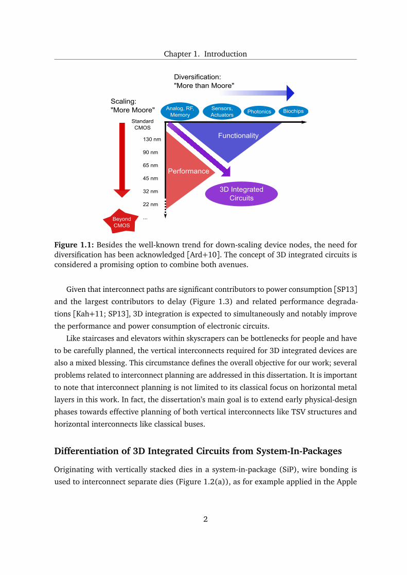
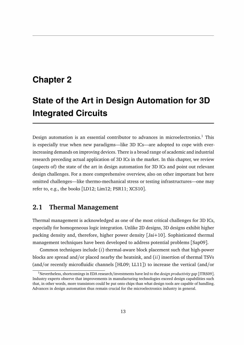
Figure 1.1: Besides the well-known trend for down-scaling device nodes, the need fordiversification has been acknowledged [Ard+10]. The concept of 3D integrated circuits isconsidered a promising option to combine both avenues.
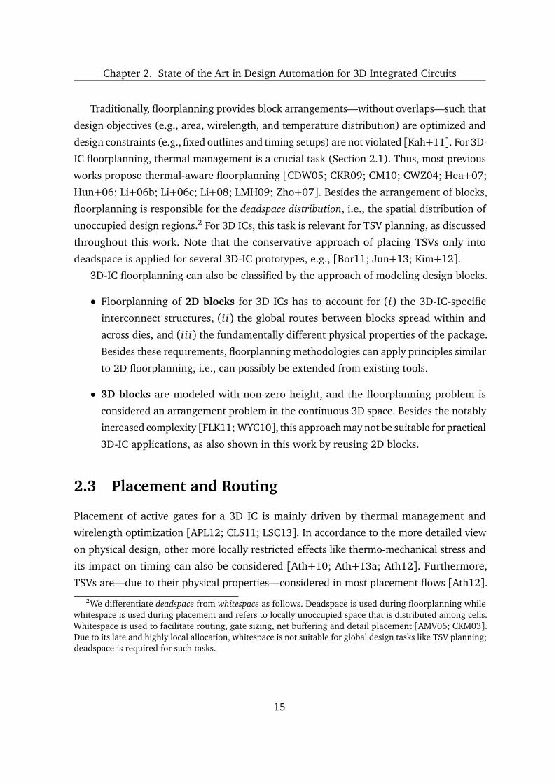
Given that interconnect paths are significant contributors to power consumption [SP13]and the largest contributors to delay (Figure 1.3) and related performance degrada-
tions [Kah+11; SP13], 3D integration is expected to simultaneously and notably improve
the performance and power consumption of electronic circuits.
Like staircases and elevators within skyscrapers can be bottlenecks for people and have
to be carefully planned, the vertical interconnects required for 3D integrated devices are
also a mixed blessing. This circumstance defines the overall objective for our work; several
problems related to interconnect planning are addressed in this dissertation. It is important
to note that interconnect planning is not limited to its classical focus on horizontal metal
layers in this work. In fact, the dissertation’s main goal is to extend early physical-design
phases towards effective planning of both vertical interconnects like TSV structures and
horizontal interconnects like classical buses.
Differentiation of 3D Integrated Circuits from System-In-Packages
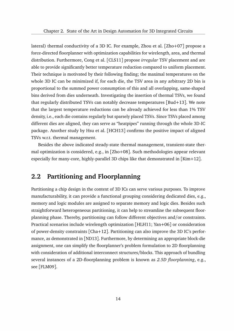
Originating with vertically stacked dies in a system-in-package (SiP), wire bonding is
used to interconnect separate dies (Figure 1.2(a)), as for example applied in the Apple
2

Chapter 1. Introduction
PackageMicrobumpWirebond
Die 1
Die 2
Die 3
(a)
Die 1
PackageBump
Die 2
Die 3
TSV
(b)
Figure 1.2: Key approaches for 3D integration of electronic devices. (a) 3D packages relyon both microbumps and wire bonding to interconnect stacked dies. (b) 3D integratedcircuited include TSVs for direct inter-die connection.
Delay
Node250 nm 180 nm 150 nm 130 nm 90 nm 65 nm
GatesInterconnects
45 nm 32 nm 22 nm
1999 2000 2001 2002 2003 2006 2007 2010 2012 Year
Figure 1.3: Gate and interconnect delays in relation to device nodes. The strong domi-nance of interconnect delays over gate delays required ongoing efforts for interconnectoptimization in the past years [ITRS09]. 3D integration, by introducing short verticalinterconnect paths, is a promising option to overcome delay-related limitations.
3

Chapter 1. Introduction
A4 SiP that places two DRAM dies on a ARM logic die [A410]. However, wire-bonding
interconnects are a limiting factor for such an SiP. Hence, the next logical step is to provide
direct die-to-die interconnect without package-level detours, resulting in 3D integrated
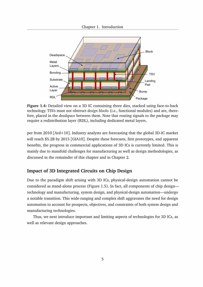
circuits (3D ICs) (Figures 1.2(b) and 1.4). Such interconnects are implemented using
through-silicon vias (TSVs)—vertical metal plugs that connect two silicon dies. The use
of TSVs enables chip-level integration, which promises shorter global interconnects while
retaining the benefits of package-level integration, e.g., heterogeneous integration.
For advanced packages, the approach of interposer-based systems is worth mentioning.
It is also referred to as 2.5D integration. Thereby, mostly pre-designed dies are stacked in
(possibly both) lateral/vertical fashion on silicon carriers—the interposers—which com-
prise metal layers and TSVs for improved interconnectivity. Interposers are mainly realized
as passive carriers, but can also include embedded components like decoupling capacitors
or even glue logic [Lau11]. Interposer-based integration is considered a cost-efficient
driver for 3D chips [Lau11; Mil+13; ZS12]. It supports various integration scenarios and
applications and is thus widely acknowledged in the current industry; notable products
include the Xilinx Virtex-7 FPGA family [Dor10] and recently a GLOBALFOUNDRIES pro-
totype containing two ARM Cortex-A9 chips [GF13]. However, the integration density of
interposer-based systems is smaller when compared to TSV-based 3D ICs.
Applications Driving 3D Integrated Circuits
3D ICs are mainly motivated by applications comprising heterogeneous modules (e.g.,
logic and memory), shorter and lower-power interconnects, as well as smaller form factors,
i.e., increased packing density [CAD10; CS09; Jun+13; Top11]. Intel presented an energy-
efficient, high-performance 80-core system with stacked SRAM [Bor11]. Another notable,
industrial project for memory-on-logic-integration is the Hybrid Memory Cube [HMC13].In the largest configuration, this IC is expected to provide a bandwidth of 320 GB/s. Some
academic 3D-IC prototypes follow the same line of heterogeneous integration [Fic+13;
Hea+10; Kim+12; Zha+10], while others promote the more challenging—particularly with
respect to (w.r.t.) thermal management (Section 2.1)—but also promising logic-on-logic
integration [Jun+13; ND13; Tho+10; TLF12; Zha+10].The International Technology Roadmap for Semiconductors (ITRS) has prominently
featured 3D ICs for some years now: e.g., in the 2009 edition, in the section on Interconnect
and the section on Assembly & Packaging [ITRS09], or in the “More-than-Moore” whitepa-
4
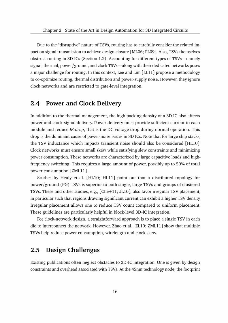
Chapter 1. Introduction
Deadspace
Substrate
Bonding
ActiveLayer
MetalLayers
RDL
TSV
LandingPad
Block
Package
Bump
Figure 1.4: Detailed view on a 3D IC containing three dies, stacked using face-to-backtechnology. TSVs must not obstruct design blocks (i.e., functional modules) and are, there-fore, placed in the deadspace between them. Note that routing signals to the package mayrequire a redistribution layer (RDL), including dedicated metal layers.
per from 2010 [Ard+10]. Industry analysts are forecasting that the global 3D-IC market
will reach $5.2B by 2015 [GIA10]. Despite these forecasts, first prototypes, and apparent
benefits, the progress in commercial applications of 3D ICs is currently limited. This is
mainly due to manifold challenges for manufacturing as well as design methodologies, as
discussed in the remainder of this chapter and in Chapter 2.
Impact of 3D Integrated Circuits on Chip Design
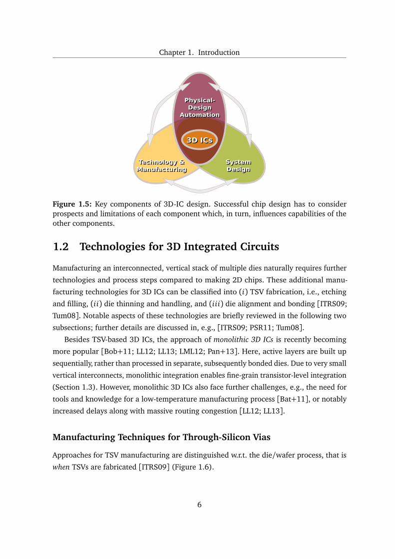
Due to the paradigm shift arising with 3D ICs, physical-design automation cannot be
considered as stand-alone process (Figure 1.5). In fact, all components of chip design—
technology and manufacturing, system design, and physical-design automation—undergo
a notable transition. This wide-ranging and complex shift aggravates the need for design
automation to account for prospects, objectives, and constraints of both system design and
manufacturing technologies.
Thus, we next introduce important and limiting aspects of technologies for 3D ICs, as
well as relevant design approaches.
5
Chapter 1. Introduction
3D ICs3D ICs
Technology &ManufacturingTechnology &
ManufacturingSystemDesignSystemDesign
Physical-Design
Automation
Physical-Design
Automation
Figure 1.5: Key components of 3D-IC design. Successful chip design has to considerprospects and limitations of each component which, in turn, influences capabilities of theother components.
1.2 Technologies for 3D Integrated Circuits
Manufacturing an interconnected, vertical stack of multiple dies naturally requires further
technologies and process steps compared to making 2D chips. These additional manu-
facturing technologies for 3D ICs can be classified into (i) TSV fabrication, i.e., etching
and filling, (ii) die thinning and handling, and (iii) die alignment and bonding [ITRS09;
Tum08]. Notable aspects of these technologies are briefly reviewed in the following two
subsections; further details are discussed in, e.g., [ITRS09; PSR11; Tum08].Besides TSV-based 3D ICs, the approach of monolithic 3D ICs is recently becoming
more popular [Bob+11; LL12; LL13; LML12; Pan+13]. Here, active layers are built up
sequentially, rather than processed in separate, subsequently bonded dies. Due to very small
vertical interconnects, monolithic integration enables fine-grain transistor-level integration
(Section 1.3). However, monolithic 3D ICs also face further challenges, e.g., the need for
tools and knowledge for a low-temperature manufacturing process [Bat+11], or notably
increased delays along with massive routing congestion [LL12; LL13].
Manufacturing Techniques for Through-Silicon Vias
Approaches for TSV manufacturing are distinguished w.r.t. the die/wafer process, that is
when TSVs are fabricated [ITRS09] (Figure 1.6).
6
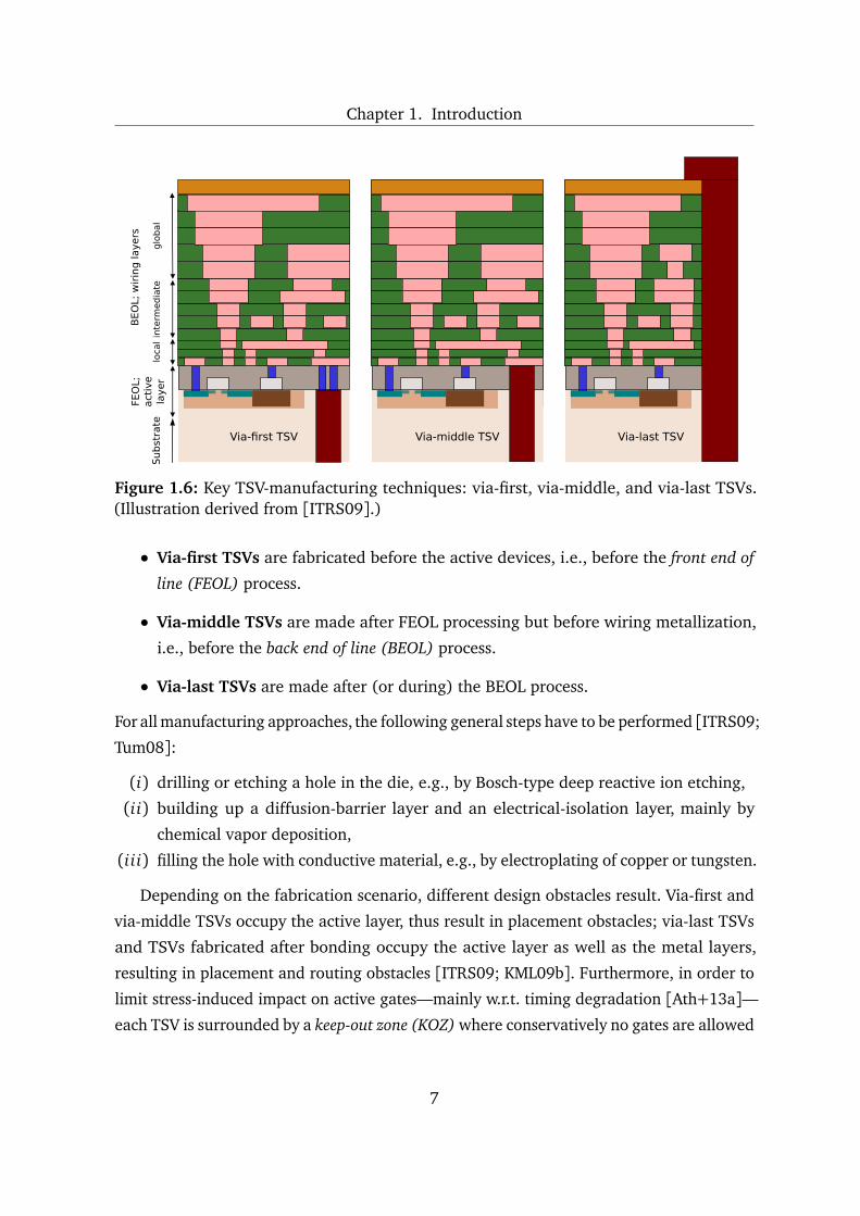
Chapter 1. IntroductionB
EO
L; w
irin
g layers
loca
lin
term
ed
iate
glo
bal
FEO
L;act
ive
layer
Subst
rate
Via-last TSVVia-middle TSVVia-first TSV
Figure 1.6: Key TSV-manufacturing techniques: via-first, via-middle, and via-last TSVs.(Illustration derived from [ITRS09].)
• Via-first TSVs are fabricated before the active devices, i.e., before the front end of
line (FEOL) process.
• Via-middle TSVs are made after FEOL processing but before wiring metallization,
i.e., before the back end of line (BEOL) process.
• Via-last TSVs are made after (or during) the BEOL process.
For all manufacturing approaches, the following general steps have to be performed [ITRS09;
Tum08]:
(i) drilling or etching a hole in the die, e.g., by Bosch-type deep reactive ion etching,
(ii) building up a diffusion-barrier layer and an electrical-isolation layer, mainly by
chemical vapor deposition,
(iii) filling the hole with conductive material, e.g., by electroplating of copper or tungsten.
Depending on the fabrication scenario, different design obstacles result. Via-first and
via-middle TSVs occupy the active layer, thus result in placement obstacles; via-last TSVs
and TSVs fabricated after bonding occupy the active layer as well as the metal layers,
resulting in placement and routing obstacles [ITRS09; KML09b]. Furthermore, in order to
limit stress-induced impact on active gates—mainly w.r.t. timing degradation [Ath+13a]—each TSV is surrounded by a keep-out zone (KOZ) where conservatively no gates are allowed
7
Chapter 1. Introduction
to be placed into. This requirement increases the TSVs’ area footprint notably; some studies
hence target and exploit the KOZ themselves, e.g., for embedding of electrostatic-discharge
protection devices [Che+12] or even for stress-aware gate placement [Ath+10]. In order
to connect TSVs with routes in the metal layers, landing pads are required. They are at
least the size of TSVs and can be even larger in order to mitigate alignment issues during
die stacking [Loi+11]. Thus, landing pads represent large routing obstacles.
Approaches for Chip Stacking and Bonding
There are manifold stacking configurations available, each having their advantages as well
as disadvantages [ITRS09; Tum08]. The classification mainly comprises wafer-to-wafer
(W2W), die-to-wafer (D2W), and die-to-die (D2D) stacking. Additionally, the orientation
of the stacked wafers/dies is differentiated: face-to-face (F2F)1 and face-to-back (F2B) are
practical scenarios, whereas back-to-back (B2B) is not commonly applied. In this context,
“face” refers to the metal layers while “back” refers to the silicon substrate of a die.
The actual bonding can be realized by either (i) oxide bonding, (ii) metal-metal
bonding, or (iii) polymer adhesive bonding [Tum08]. For metal-metal bonding, one differ-
entiates between metal-fusion bonding and metal-eutectic bonding (e.g., with copper-tin
phases). These different bonding options also have their specific benefits and drawbacks;
see [Tum08] for details.
Depending on the stacking configuration, TSV fabrication, die thinning, die bonding,
as well as carrier die bonding/debonding, have to follow a particular order [ITRS09].
1.3 Design Approaches for 3D Integrated Circuits
Design approaches can be characterized by their granularity, i.e., the applied partition-
ing scheme, defining which circuit parts are potentially split and assigned to different
dies [LXB07]. On the opposite ends of the related granularity scale, the approaches of
transistor-level (finest-grain) integration vs. core-level (coarsest-grain) integration can be
found. Only recently—mainly due to advances in manufacturing technologies—transistor-
level integration becomes applicable [Bob+11; LL12; LML12; Pan+13]. It is expected to
1Note that F2F stacking of two dies represents an interesting option for (small-scale) 3D ICs; thisconfiguration does not require TSVs since the dies’ metal layers are facing each other and can thus beinterconnected with regular-sized vias or microbumps [Fic+13; TLF12; Zha+10].
8
Chapter 1. Introduction
(b)(a)
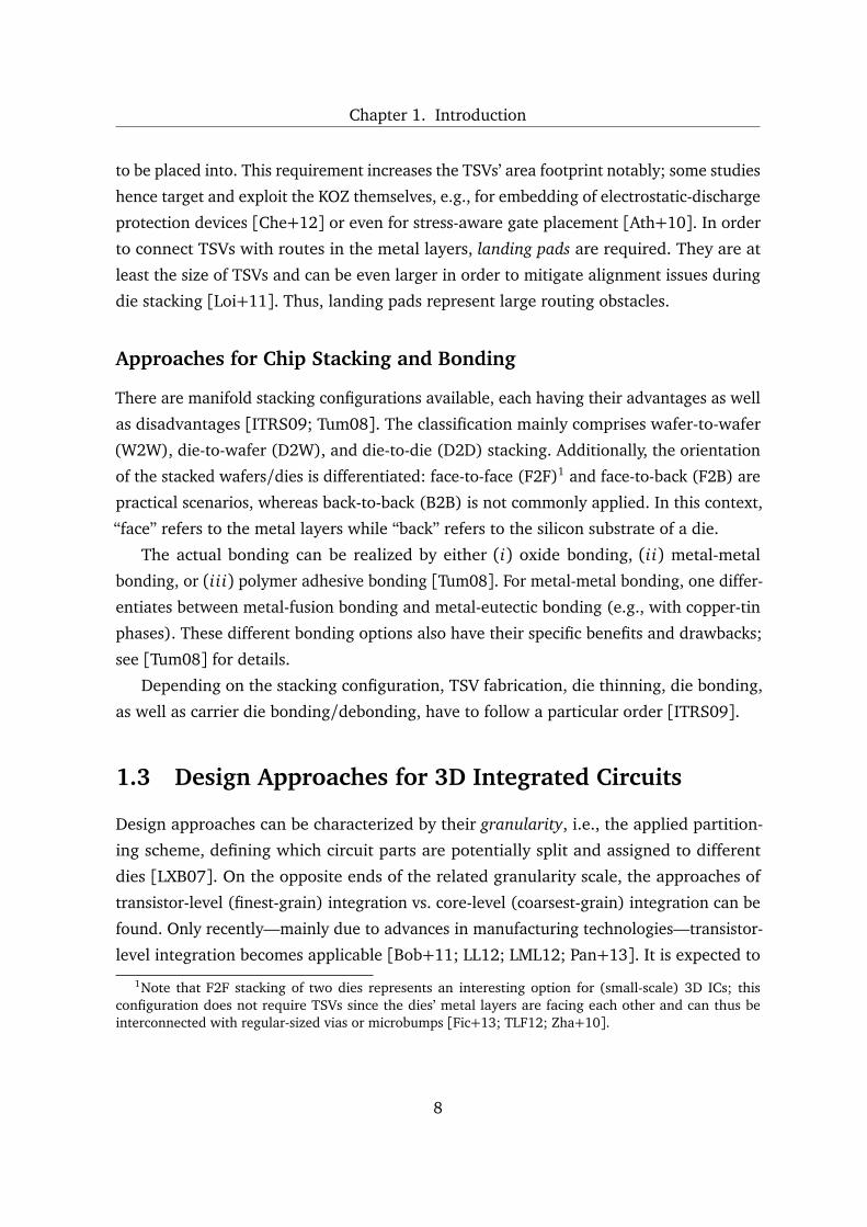
Figure 1.7: Relevant design approaches for 3D ICs. TSVs are illustrated as solid, red boxesand landing pads as dashed, red boxes. F2B stacking is considered; TSVs cannot obstructblocks in lower dies but landing pads overlap with blocks in upper dies, due to illustrationperspective. (a) Gate-level integration, enlarged for illustration. It is based on placingseparate gates on multiple dies. (b) Block-level integration relies on 2D blocks, which arepartitioned between multiple dies and connected through global routes.
provide large performance benefits due to the tight and thus short-path vertical coupling of
(partial) transistors. Besides the high demands on very-small-scale vias and other related
challenges, this style requires a full redesign, i.e., completely prevents design reuse. On
the other hand, for core-level integration, the efforts are comparable to traditional 2D chip
design; only few inter-core connects have to be realized by placing and wiring TSVs. Apart
from that, the cores can be fully reused. In consequence, the gained benefits are low; the
properties of such a 3D IC are still dominated by their separate but stacked 2D chips.
Next, we contrast relevant design approaches for 3D ICs, found in the middle of the
granularity scale: gate-level and block-level integration (Figure 1.7).
Gate-Level Integration
One approach for 3D-IC design is to partition standard cells between multiple dies and
use TSVs in routes that connect cells spread among the active layers. This integration style
promises significant wirelength reduction and great flexibility [LXB07; NC11; ND13].Its adverse effects include, for example, the massive number of necessary TSVs for
random logic. Studies by Kim et al. [KML09b], and Mak and Chu [MC12] reveal that
partitioning gates between multiple dies may undermine wirelength reduction unless circuit
modules of certain minimal size are preserved and/or TSVs are down-scaled. Another
9
Chapter 1. Introduction
study [NM11] points out that layout effects can largely influence performance for highly
regular blocks such as SRAM registers; a mismatch between TSV and cell dimensions may
introduce wirelength disparities while routing regular structures to TSVs. Timing-aware
placement of partitioned gates is required for design closure [LL10]; this timing issue is
intensified by inter-die variation mismatches [GM09]. Besides, partitioning a design block
across multiple dies requires new pre-bond testing approaches [LC09; LL09]. After die
stacking, a single failed die renders the whole 3D IC unusable, thus easily undermining
overall yield.
Furthermore, gate-level 3D integration requires redesign of all available intellectual
property (IP), since existing IP blocks and electronic design automation (EDA) tools do not
account for 3D integration. Even when 3D (gate-level) place-and-route tools appear on
the market, it will take many years for IP vendors to upgrade their extensive IP portfolios
for 3D integration.
In summary, gate-level integration may be very promising in terms of design flexibility,
performance, and wirelength reduction, but it faces multiple challenges and currently
appears—like with transistor-level integration—only applicable in a limited scope. Practical
scenarios include devices with high demands on efficiency and low power, as demonstrated
with designs comprising, e.g., complex modules like floating-point units and long-path
multipliers [ND13; Tho+10; TLF12].
Block-Level Integration
Blocks typically subsume most of a design’s connectivity and are linked by a small number
of global interconnects [SK00]. Therefore, block-level integration promises to reduce TSV
overhead by assigning only few global interconnects to them. In this context, it is also
notable that TSVs do not scale at the same rate as transistors, thus the TSV-to-cell mismatch
will likely remain for future nodes and may even increase [NM11].Sophisticated 3D systems combining heterogeneous dies are anticipated in a whitepaper
by Cadence [CAD10]. Such devices require distinct manufacturing processes at different
technology nodes for fast and low-power random logic, several memory types, analog
and RF circuits, on-chip sensors, micro-electro-mechanical systems, and so on. Block-
level integration is imperative for such heterogeneous 3D ICs where modules cannot be
partitioned among different-technology dies.
10

Chapter 1. Introduction
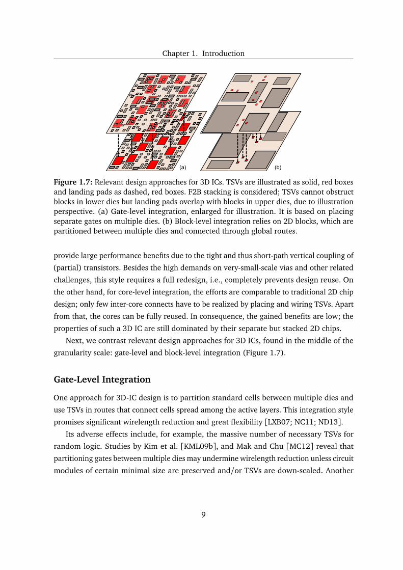
(a) (b)
Figure 1.8: Block-level integration for 3D ICs. (a) The R2D style uses predefined TSV sites(small red boxes) within the block footprints. (b) The L2D style distributes TSVs preferablybetween blocks, thus easing design efforts and limiting stress for gates.
When assigning entire blocks to separate dies and connecting them with TSVs, we can
distinguish two design styles (Figure 1.8).
• Redesigned 2D (R2D) style: 2D blocks designed for 3D integration, TSVs can be
included within the footprints.
• Legacy 2D (L2D) style: 2D blocks not designed for 3D integration, TSVs are prefer-
ably placed between blocks.
The relevant style has to be selected depending on the type of given IP blocks. For hard IP
blocks with optimized and fixed layout, L2D would be chosen. For soft IP blocks, i.e., blocks
given in behavioral description and synthesized during the design flow, the R2D style
appears more appropriate (but also challenging, see Section 4.1). Note that the R2D style
can be more constrained; for B2B stacking, blocks may be required to align according to
their predefined TSV locations, which would naturally increase floorplanning complexity.
This may further complicate design closure, e.g., due to routing congestion around densely
packed blocks and/or TSVs.
Further benefits of both R2D and L2D styles are described next. Design-for-testability
(DFT) structures are a key component of existing IP blocks and can be used to realize pre-
bond and post-bond testing [LC09]. In general, test pins can be provisioned on each die and
multiplexed/shared with other pins for pre- and post-bond testing [Jia+09]. Block-level
integration can be used to efficiently reduce critical paths, thus simultaneously allowing
limited signal delay, increased performance and reduced power consumption [Ath+13b;
11
Chapter 1. Introduction
KTL12; LL10; LXB07]. With block-level integration, critical paths are mostly located within
2D blocks—they do not traverse multiple active layers, which limits the impact of process
variations on performance [GM13]. In [FRB07], the authors propose optimal matching
of “slow dies” and “fast dies”, based on accurate delay models with process variations
considered. This approach assumes that dies can be delay-tested before stacking—a strong
argument for block-level integration where dies are restricted to self-contained modules.
Another aspect of block-level integration deals with design effort. Modern chip design
mostly relies on pre-designed and optimized IP blocks. Analysts at Gartner Dataquest point
out that the IP market is still growing and will reach $2.3B by 2014 [Bro11]. Redesigning
existing IP blocks to be spread out on multiple dies is not practical; such a redesign would
require new 3D-EDA tools for physical design and verification, increasing risks of design
failures and being late to market. Considering the successful track record of 2D-IP blocks
in applications and at the marketplace, it is more convenient to use available legacy IP
blocks. In the L2D style, which is mandatory for hard blocks, risks are further limited by
placing TSVs only between blocks, mitigating the TSVs’ impact on active gates.
12
Chapter 2
State of the Art in Design Automation for 3DIntegrated Circuits
Design automation is an essential contributor to advances in microelectronics.1 This
is especially true when new paradigms—like 3D ICs—are adopted to cope with ever-
increasing demands on improving devices. There is a broad range of academic and industrial
research preceding actual application of 3D ICs in the market. In this chapter, we review
(aspects of) the state of the art in design automation for 3D ICs and point out relevant
design challenges. For a more comprehensive overview, also on other important but here
omitted challenges—like thermo-mechanical stress or testing infrastructures—one may
refer to, e.g., the books [LD12; Lim12; PSR11; XCS10].
2.1 Thermal Management
Thermal management is acknowledged as one of the most critical challenges for 3D ICs,
especially for homogeneous logic integration. Unlike 2D designs, 3D designs exhibit higher
packing density and, therefore, higher power density [Jai+10]. Sophisticated thermal
management techniques have been developed to address potential problems [Sap09].Common techniques include (i) thermal-aware block placement such that high-power
blocks are spread and/or placed nearby the heatsink, and (ii) insertion of thermal TSVs
(and/or recently microfluidic channels [HL09; LL11]) to increase the vertical (and/or
1Nevertheless, shortcomings in EDA research/investments have led to the design productivity gap [ITRS09].Industry experts observe that improvements in manufacturing technologies exceed design capabilities suchthat, in other words, more transistors could be put onto chips than what design tools are capable of handling.Advances in design automation thus remain crucial for the microelectronics industry in general.
13
Chapter 2. State of the Art in Design Automation for 3D Integrated Circuits
lateral) thermal conductivity of a 3D IC. For example, Zhou et al. [Zho+07] propose a
force-directed floorplanner with optimization capabilities for wirelength, area, and thermal
distribution. Furthermore, Cong et al. [CLS11] propose irregular TSV placement and are
able to provide significantly better temperature reduction compared to uniform placement.
Their technique is motivated by their following finding; the maximal temperatures on the
whole 3D IC can be minimized if, for each die, the TSV area in any arbitrary 2D bin is
proportional to the summed power consumption of this and all overlapping, same-shaped
bins derived from dies underneath. Investigating the insertion of thermal TSVs, we found
that regularly distributed TSVs can notably decrease temperatures [Bud+13]. We note
that the largest temperature reductions can be already achieved for less than 1% TSV
density, i.e., each die contains regularly but sparsely placed TSVs. Since TSVs placed among
different dies are aligned, they can serve as “heatpipes” running through the whole 3D-IC
package. Another study by Hsu et al. [HCH13] confirms the positive impact of aligned
TSVs w.r.t. thermal management.
Besides the above indicated steady-state thermal management, transient-state ther-
mal optimization is considered, e.g., in [Zho+08]. Such methodologies appear relevant
especially for many-core, highly-parallel 3D chips like that demonstrated in [Kim+12].
2.2 Partitioning and Floorplanning
Partitioning a chip design in the context of 3D ICs can serve various purposes. To improve
manufacturability, it can provide a functional grouping considering dedicated dies, e.g.,
memory and logic modules are assigned to separate memory and logic dies. Besides such
straightforward heterogeneous partitioning, it can help to streamline the subsequent floor-
planning phase. Thereby, partitioning can follow different objectives and/or constraints.
Practical scenarios include wirelength optimization [HLH11; Yan+06] or consideration
of power-density constraints [Cha+12]. Partitioning can also improve the 3D IC’s perfor-
mance, as demonstrated in [ND13]. Furthermore, by determining an appropriate block-die
assignment, one can simplify the floorplanner’s problem formulation to 2D floorplanning
with consideration of additional interconnect structures/blocks. This approach of bundling
several instances of a 2D-floorplanning problem is known as 2.5D floorplanning, e.g.,
see [FLM09].
14
Chapter 2. State of the Art in Design Automation for 3D Integrated Circuits
Traditionally, floorplanning provides block arrangements—without overlaps—such that
design objectives (e.g., area, wirelength, and temperature distribution) are optimized and
design constraints (e.g., fixed outlines and timing setups) are not violated [Kah+11]. For 3D-
IC floorplanning, thermal management is a crucial task (Section 2.1). Thus, most previous
works propose thermal-aware floorplanning [CDW05; CKR09; CM10; CWZ04; Hea+07;
Hun+06; Li+06b; Li+06c; Li+08; LMH09; Zho+07]. Besides the arrangement of blocks,
floorplanning is responsible for the deadspace distribution, i.e., the spatial distribution of
unoccupied design regions.2 For 3D ICs, this task is relevant for TSV planning, as discussed
throughout this work. Note that the conservative approach of placing TSVs only into
deadspace is applied for several 3D-IC prototypes, e.g., [Bor11; Jun+13; Kim+12].3D-IC floorplanning can also be classified by the approach of modeling design blocks.
• Floorplanning of 2D blocks for 3D ICs has to account for (i) the 3D-IC-specific
interconnect structures, (ii) the global routes between blocks spread within and
across dies, and (iii) the fundamentally different physical properties of the package.
Besides these requirements, floorplanning methodologies can apply principles similar
to 2D floorplanning, i.e., can possibly be extended from existing tools.
• 3D blocks are modeled with non-zero height, and the floorplanning problem is
considered an arrangement problem in the continuous 3D space. Besides the notably
increased complexity [FLK11; WYC10], this approach may not be suitable for practical
3D-IC applications, as also shown in this work by reusing 2D blocks.
2.3 Placement and Routing
Placement of active gates for a 3D IC is mainly driven by thermal management and
wirelength optimization [APL12; CLS11; LSC13]. In accordance to the more detailed view
on physical design, other more locally restricted effects like thermo-mechanical stress and
its impact on timing can also be considered [Ath+10; Ath+13a; Ath12]. Furthermore,
TSVs are—due to their physical properties—considered in most placement flows [Ath12].
2We differentiate deadspace from whitespace as follows. Deadspace is used during floorplanning whilewhitespace is used during placement and refers to locally unoccupied space that is distributed among cells.Whitespace is used to facilitate routing, gate sizing, net buffering and detail placement [AMV06; CKM03].Due to its late and highly local allocation, whitespace is not suitable for global design tasks like TSV planning;deadspace is required for such tasks.
15
Chapter 2. State of the Art in Design Automation for 3D Integrated Circuits
Due to the “disruptive” nature of TSVs, routing has to carefully consider the related im-
pact on signal transmission to achieve design closure [ML06; PL09]. Also, TSVs themselves
obstruct routing in 3D ICs (Section 1.2). Accounting for different types of TSVs—namely
signal, thermal, power/ground, and clock TSVs—along with their dedicated networks poses
a major challenge for routing. In this context, Lee and Lim [LL11] propose a methodology
to co-optimize routing, thermal distribution and power-supply noise. However, they ignore
clock networks and are restricted to gate-level integration.
2.4 Power and Clock Delivery
In addition to the thermal management, the high packing density of a 3D IC also affects
power and clock-signal delivery. Power delivery must provide sufficient current to each
module and reduce IR-drop, that is the DC voltage drop during normal operation. This
drop is the dominant cause of power-noise issues in 3D ICs. Note that for large chip stacks,
the TSV inductance which impacts transient noise should also be considered [HL10].Clock networks must ensure small skew while satisfying slew constraints and minimizing
power consumption. These networks are characterized by large capacitive loads and high-
frequency switching. This requires a large amount of power, possibly up to 50% of total
power consumption [ZML11].Studies by Healy et al. [HL10; HL11] point out that a distributed topology for
power/ground (PG) TSVs is superior to both single, large TSVs and groups of clustered
TSVs. These and other studies, e.g., [Che+11; JL10], also favor irregular TSV placement,
in particular such that regions drawing significant current can exhibit a higher TSV density.
Irregular placement allows one to reduce TSV count compared to uniform placement.
These guidelines are particularly helpful in block-level 3D-IC integration.
For clock-network design, a straightforward approach is to place a single TSV in each
die to interconnect the network. However, Zhao et al. [ZL10; ZML11] show that multiple
TSVs help reduce power consumption, wirelength and clock skew.
2.5 Design Challenges
Existing publications often neglect obstacles to 3D-IC integration. One is given by design
constraints and overhead associated with TSVs. At the 45nm technology node, the footprint
16

Chapter 2. State of the Art in Design Automation for 3D Integrated Circuits
of a 10µm × 10µm TSV is comparable to that of about 50 gates [KML09b]. Furthermore,
manufacturability demands large landing pads and keep-out zones (Section 1.2). Previous
work in physical design often neglects this area overhead [CWZ04; Hun+06; Li+06b;
Li+06c; LMH09; Sri+09; Zho+07]. Some studies explicitly consider thermal TSV insertion
but not signal TSVs [Li+06c; Li+08; WL07]. Tsai et al. [TWH11] observe that previous
work also neglects the impact of TSV locations on wirelength estimates for floorplanning.
While the use of TSVs is generally expected to reduce wirelength of 3D ICs compared to
2D ICs, Kim et al. [KML09b] report that reductions vary depending on the number of TSVs
and their properties. They point out that TSV insertion increases silicon area and/or routing
congestion, thereby possibly making wires longer. Hence, excessive usage of TSVs can
undermine their potential advantages, and the study shows that this trade-off is controlled
by the granularity of inter-die partitioning. Wirelength typically decreases for block-level
(coarse/moderate) granularities, but increases for gate-level (fine) granularities.
A further impediment to 3D integration—the impact of design partitioning—is more
subtle. To achieve higher overall yield, separate testing of independent dies is essen-
tial [Bor11; LC09]. However, tight integration between functional parts of a design entails
a significant amount of interconnect between different sections of the same circuit mod-
ule that were partitioned to different dies. Aside from the massive overhead introduced
by required TSVs, sections of such a module, e.g., a multiplier, demand for new testing
approaches [LC09; LL09]. Additionally, another study [GM09] points out that intra-die
variation becomes a first-order effect for 3D-IC integration, while being only a second-order
effect for 2D chips.3 The authors estimate that a 3D layout may yield more poorly than the
same circuit laid out in 2D, contrary to the original promise of 3D integration.
These wide-ranging considerations suggest that a successful approach to 3D-IC inte-
gration must rely on effective design methodologies. In this dissertation, we propose and
evaluate methodologies focused on interconnect planning for physical design of 3D inte-
grated circuits; our specific research objectives are given in the next chapter.
3When a die experiences process variation, all transistors become faster/slower, perhaps at a differentrate. The variations in transistor performance are, therefore, a second-order effect. However, several stackeddies may experience systematic variations in opposite directions—a first-order effect. This issue can beespecially challenging for clock signals which are spread throughout the whole 3D IC [GM13; Yan+11].
17
Chapter 3
Research Objectives
The commercial acceptance of 3D ICs is currently behind its expectations, mainly due
to challenges regarding manufacturing and integration technologies, as well as design
automation (Chapters 1 and 2). To ease the transition towards 3D ICs, the following
particular design challenges are addressed in this dissertation:
1. increasing the limited reusability of available, trustworthy 2D-IP blocks,
2. the planning of different types of TSVs with focus on design quality, and
3. the structural planning of massively-parallel, 3D-IC-specific interconnects.
Approaching these research challenges serves one unified objective, that is the intercon-
nect planning for physical design of 3D integrated circuits. Recall that interconnect planning
is not limited to its classical focus on horizontal metal layers in this work. Instead, we
extend physical design for effective planning of both vertical and horizontal interconnect
structures. Therefore, we propose efficient and effective methodologies for early and/or
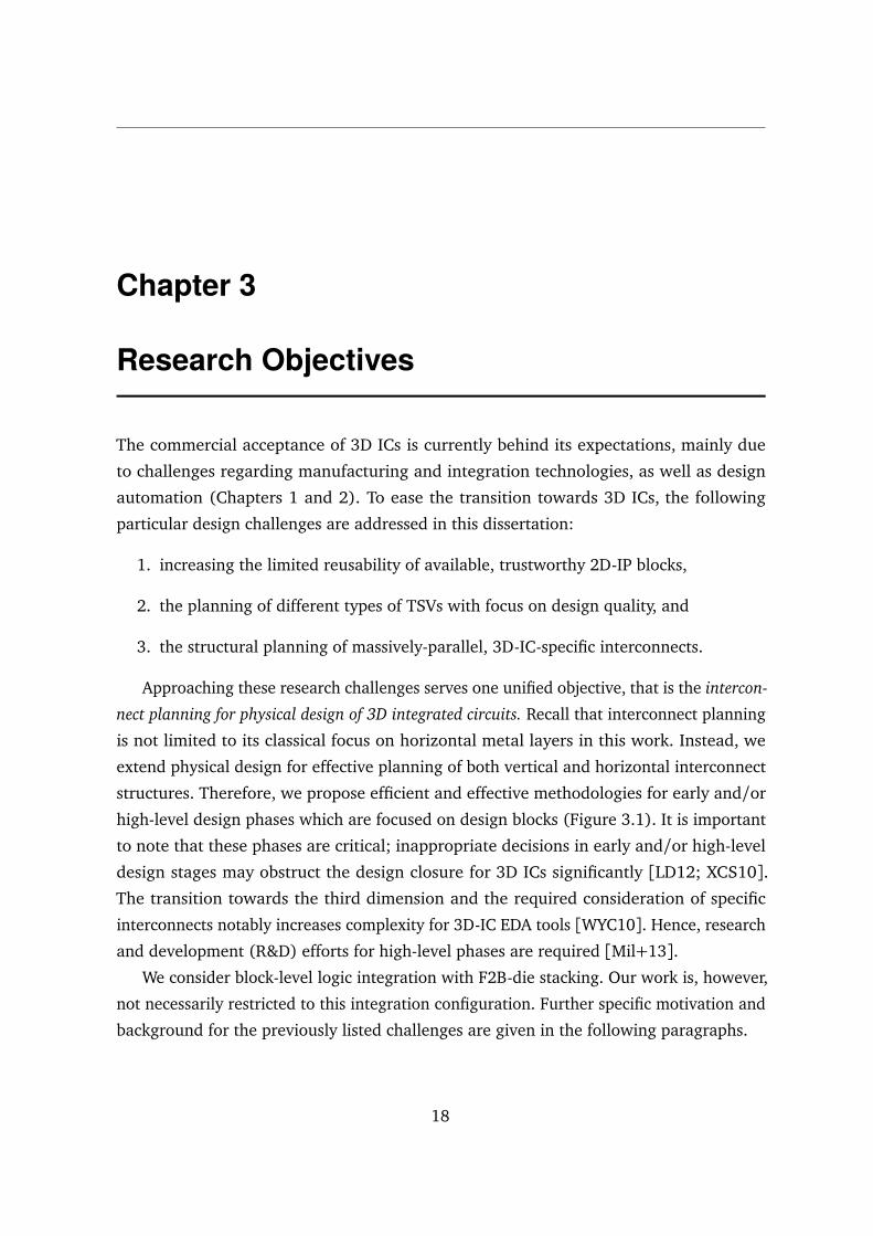
high-level design phases which are focused on design blocks (Figure 3.1). It is important
to note that these phases are critical; inappropriate decisions in early and/or high-level
design stages may obstruct the design closure for 3D ICs significantly [LD12; XCS10].The transition towards the third dimension and the required consideration of specific
interconnects notably increases complexity for 3D-IC EDA tools [WYC10]. Hence, research
and development (R&D) efforts for high-level phases are required [Mil+13].We consider block-level logic integration with F2B-die stacking. Our work is, however,
not necessarily restricted to this integration configuration. Further specific motivation and
background for the previously listed challenges are given in the following paragraphs.
18
Chapter 3. Research Objectives
System Definitionand
Architectural Design
Behavioral Descriptionand
Logic Design
Circuit Design
Physical Design
Manufacturingand
Testing
Packackingand
Final Testing
Floorplanning
Partitioning
Design ofPG and Clock Networks
Placement
Design of Buses andGlobal Networks
Timing Closure
Physical Verificationand
Signoff
Routing
Sco
pe o
f D
isse
rtati
on:
Inte
rconnect
Pla
nn
ing
for
(Earl
y P
hase
s of)
Physi
cal D
esi
gn o
f 3
D IC
s
Figure 3.1: A 3D-IC design flow with focus on physical design. Network-design steps area prerequisite for placement and routing; these steps are responsible for planning of TSVsand/or global interconnects. The dissertation’s scope is outlined; most early physical-designsteps are extended for interconnect planning.
19
Chapter 3. Research Objectives
While tackling the problem of limited IP-reusabiltiy (Chapter 4), we initially address
basic principles of assembling and connecting 2D-IP blocks within new 3D-IC design.
Due to the wide-spread integration of IP blocks in classical chip-design flows, this is an
indispensable challenge. We show how to integrate 2D-IP blocks into 3D ICs without
altering their layout, i.e., how to simultaneously account for blocks and TSVs during
and/or after floorplanning. In this context, we promote the planning of TSV islands, i.e.,
grouped bundles of TSVs, for locally limited impact of TSVs on design planning and quality.
For the problem of planning different types of TSVs (Chapter 5), we consider a more
comprehensive view on design quality. In fact, we found that different types of TSVs and
their placement have manifold implications on 3D-IC design quality. However, we also
found that these different criteria can be unified; by managing the deadspace distribution
in accordance with TSV planning, we achieve multiobjective design optimization for 3D
ICs. To realize this, we propose a design-flow extension which can be plugged in after
floorplanning. It includes techniques for (i) planning different types of TSVs, (ii) deadspace
management, as well as (iii) design-quality analysis.
Concerning problem three (Chapter 6), we account for the fact that massively-parallel
3D ICs rely on massive interconnect structures, running between blocks spread among
one or multiple dies. We observe that structural planning of such interconnects has been
previously ignored during early design steps, consequently impeding the interconnects’
routing in subsequent steps. In our approach, structural planning of interconnects is
seamlessly integrated into 3D floorplanning by means of block alignment. Our provided
floorplanning suite has also proven to be competitive in other key objectives for 3D designs
like fast thermal management and fixed-outline floorplanning.
We address the introduced problems and our related solutions in detail in the next
three Chapters (4–6). Our research conclusions, including an illustrative overview of the
dissertation’s contributions (Figure 7.1, p. 103), are given in Chapter 7.
20
Chapter 4
Planning Through-Silicon Via Islands forBlock-Level Design Reuse*
Despite numerous advantages of 3D ICs, their commercial success remains limited. In
part, this is due to the wide availability of trustworthy IP blocks developed for 2D ICs and
proven through repeated use. Block-based design reuse may thus ease 3D integration, as
elaborated in Section 1.3, but it is nonetheless challenging.
In this chapter, we show how to integrate 2D-IP blocks into 3D ICs without altering
their layout. Recall that TSVs represent routing and/or placement obstacles. Therefore, we
promote a design style based on grouping TSVs into islands in order to spatially limit the
obstructions introduced by TSVs. Experiments indicate that the overhead of our proposed
integration is tolerable, which can help accelerate industry adoption of 3D-IC designs.
4.1 Problems for Design Reuse in 3D Integrated Circuits
As discussed in Section 2.5, TSVs introduce design constraints and overheads, mainly due
to their (to gates comparably large) dimensions and intrusive character when “injected”
into silicon dies. In fact, TSVs must not obstruct hard 2D-IP blocks; the optimized and
fixed layout of such blocks cannot include large TSVs simply because the blocks’ design
was not accounting for TSVs. This mutual exclusion of TSVs and IP blocks can also be
* Parts of this chapter have been published in [KML11; KML12] as well as in German in [KL11; Kne12].
21

Chapter 4. Planning Through-Silicon Via Islands for Block-Level Design Reuse
(a) (b)
Figure 4.1: TSV-placement styles. Recall that we consider F2B integration; TSVs cannotobstruct blocks in lower dies but TSV landing pads overlap with blocks in upper dies, due toillustration perspective. TSV islands are illustrated as brown, dashed boxes containing TSVs(solid, red boxes). Landing pads are illustrated as dashed, red boxes. (a) One approach isto place scattered TSVs between blocks. (b) Another approach is our proposed L2Di stylefor 3D integration where TSVs are grouped into TSV islands.
applied while reusing soft, to be synthesized blocks—although design tools may account
for TSVs within such soft blocks, this is not necessarily practical.1
To connect blocks placed among multiple dies, required TSVs can be inserted in several
ways without disturbing the IP blocks’ layout. First, one could use single, spread out TSVs
(Figure 4.1(a)), as applied in, e.g., [He+09; LL11; Pat+10]. The second option is to place
TSVs on a gridded structure, see for example [KAL09; KML09b; Liu+13]. A study by Kim
et al. [KAL09] compares placing TSVs on a grid (regular placement) to placing scattered
TSVs (irregular placement). The study reveals that irregular placement performs better
in terms of wirelength reduction and design runtime. The third option groups several
TSVs into TSV islands as proposed for our design style called legacy 2D integrated with
TSV islands (L2Di) (Figure 4.1(b)). Further studies considering some type of grouped
TSVs are, e.g., [HL12; Kim+12; KTL12; Mil+13; TWH11; ZL12]. Depending on the TSV
manufacturing process, all TSV-insertion styles might require a minimum TSV density as
well as specific configurations for pitch and spacing.
1Inserting TSVs into densely packed design blocks is expected to complicate design closure since it(i) introduces placement and routing obstacles [KML09b], (ii) induces notable stress for nearby activegates [Yan+10], and (iii) requires design tools to provide sophisticated TSV-related verification, e.g., signal-integrity analysis considering coupling between TSVs [Liu+11; LSL11; Yao+13].
22

Chapter 4. Planning Through-Silicon Via Islands for Block-Level Design Reuse
4.2 Connecting Blocks Using Through-Silicon Via Islands
Viewing TSVs as purely geometric objects would neglect several key technology issues.
These include silicon stress in the neighborhood of TSVs—which alters transistor proper-
ties and motivates keep-out zones [Ath+10; Jao+12; Yan+10]—or reliability and fault-
tolerance issues for TSVs themselves [Hsi+10; Loi+08; Pan+12]. Regular TSV structures
can be designed to address these concerns by optimizing spacing between TSVs, possibly
sharing keep-out zones, and performing electro-thermal and mechanical simulations be-
fore layout synthesis [Lu+09; ZL11]. In contrast, single TSVs would require greater care
during layout. To this end, regular placement helps manufacturing reliable TSVs [Hea+10;
Hsi+10], which favors assembling multiple TSVs into TSV islands. Figure 4.1(b) illustrates
TSV islands as blocks with densely placed TSVs. Overall, grouping TSVs and optimizing
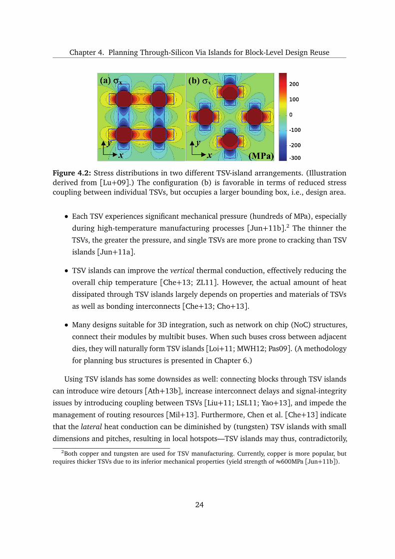
the layout of resulting islands provides several benefits, which are summarized below.
• TSVs introduce stress in the surrounding silicon which affects nearby transis-
tors [Ath+10; Jao+12; Yan+10], but TSV islands do not need to include active
gates. The layout of these islands can be optimized in advance [Lu+09; ZL11] (Fig-
ure 4.2); regular island structures help to limit stress below the yielding strength of
copper [Jun+11b]. Furthermore, using TSV islands limits stress to particular design
regions [Jun+11b; Jun+12; Lu+09]. Placing islands between blocks may thus limit
stress on blocks’ active gates. Additionally, the stress correlation between TSV islands
and package bumps can be analysed efficiently, as shown in [JPL12].
• TSV islands facilitate redundancy architectures [Hsi+10; Loi+08], where failed TSVs
are shifted within a chain structure or dynamically rerouted to spare TSVs. (Note
that Figure 4.1(b) illustrates islands of four TSVs, including a spare.)
• Grouping TSVs can reduce area overhead. TSVs can be packed densely within TSV
islands, possibly reducing keep-out zones without increasing stress-induced impact
on active gates [Lu+09].
• Regular layouts of pre-designed TSV islands can improve manufacturability by in-
creasing exposure quality during TSV lithography [Hsi+10].
23
Chapter 4. Planning Through-Silicon Via Islands for Block-Level Design Reuse
200
100
0
-100
-200
-300
200
100
0
-100
-200
-300
Figure 4.2: Stress distributions in two different TSV-island arrangements. (Illustrationderived from [Lu+09].) The configuration (b) is favorable in terms of reduced stresscoupling between individual TSVs, but occupies a larger bounding box, i.e., design area.
• Each TSV experiences significant mechanical pressure (hundreds of MPa), especially
during high-temperature manufacturing processes [Jun+11b].2 The thinner the
TSVs, the greater the pressure, and single TSVs are more prone to cracking than TSV
islands [Jun+11a].
• TSV islands can improve the vertical thermal conduction, effectively reducing the
overall chip temperature [Che+13; ZL11]. However, the actual amount of heat
dissipated through TSV islands largely depends on properties and materials of TSVs
as well as bonding interconnects [Che+13; Cho+13].
• Many designs suitable for 3D integration, such as network on chip (NoC) structures,
connect their modules by multibit buses. When such buses cross between adjacent
dies, they will naturally form TSV islands [Loi+11; MWH12; Pas09]. (A methodology
for planning bus structures is presented in Chapter 6.)
Using TSV islands has some downsides as well: connecting blocks through TSV islands
can introduce wire detours [Ath+13b], increase interconnect delays and signal-integrity
issues by introducing coupling between TSVs [Liu+11; LSL11; Yao+13], and impede the
management of routing resources [Mil+13]. Furthermore, Chen et al. [Che+13] indicate
that the lateral heat conduction can be diminished by (tungsten) TSV islands with small
dimensions and pitches, resulting in local hotspots—TSV islands may thus, contradictorily,
2Both copper and tungsten are used for TSV manufacturing. Currently, copper is more popular, butrequires thicker TSVs due to its inferior mechanical properties (yield strength of ≈600MPa [Jun+11b]).
24

Chapter 4. Planning Through-Silicon Via Islands for Block-Level Design Reuse
aggravate heat dissipation. Overall, the relevance and/or feasibility of TSV islands depends
on technology details, which currently vary significantly among different manufacturers.
The consideration of large TSV islands may complicate floorplanning and placement.
To address these challenges, we develop sophisticated algorithms for net assignment and
TSV-island insertion in the remainder of this chapter. Furthermore, we allow trivial TSV
islands with only one TSV as well. This subsumes the straightforward handling of TSVs as
special case, thus our proposal is not restrictive.
4.2.1 Problem Formulation and Methodology Overview
As mentioned in Section 2.5, previous work on 3D floorplanning often neglects design
constraints and overhead associated with TSVs. However, these studies promise to provide
optimized floorplans in terms of, e.g., minimal wirelength and thermal distribution. There-
fore, 3D integration following the L2Di style addresses the omission of TSV planning. It
seeks to cluster inter-die nets into TSV islands without incurring excessive overhead. Such
TSV islands, as well as single TSVs, are then inserted into deadspace around floorplan
blocks. If TSV-island insertion is impossible due to lack of deadspace, blocks can be shifted
from their initial locations without disturbing their ordering. Additional deadspace can be
inserted when necessary.
For 3D integration considering our L2Di style, the following input is assumed.
• Dies / active layers, denoted as set D. Each die d ∈ D has dimensions (hd , wd) such
that every block assigned to d can fit in the outline without incurring overlap.
• Rectangular IP blocks, denoted as set B. Each block b ∈ B has dimensions (hb, wb)and pins, denoted as set P b. Each pin p ∈ P b of block b is defined by its offset
δxp ,δ y
p
w.r.t. the block’s geometric center (origin).
• Boundary pins, denoted as set P. Each pin p ∈ P is defined by its coordinates
xp, yp
w.r.t. the 3D IC’s lower left corner.
• Netlist, denoted as set N . A net n ∈ N describes a connection between two or more
pins.
• TSV-island types, denoted as set T . Each type t ∈ T has dimensions (ht , wt) and
capacity κt . Since pre-designed TSV-island types may incorporate spare TSVs, κt
defines the number of nets that can be routed through t.
25
Chapter 4. Planning Through-Silicon Via Islands for Block-Level Design Reuse
• 3D floorplan, denoted as set F . Each block b is assigned a location (xb, yb, db) such
that no blocks overlap. The coordinate of the block’s origin is denoted as (xb, yb)and db denotes the assigned die.
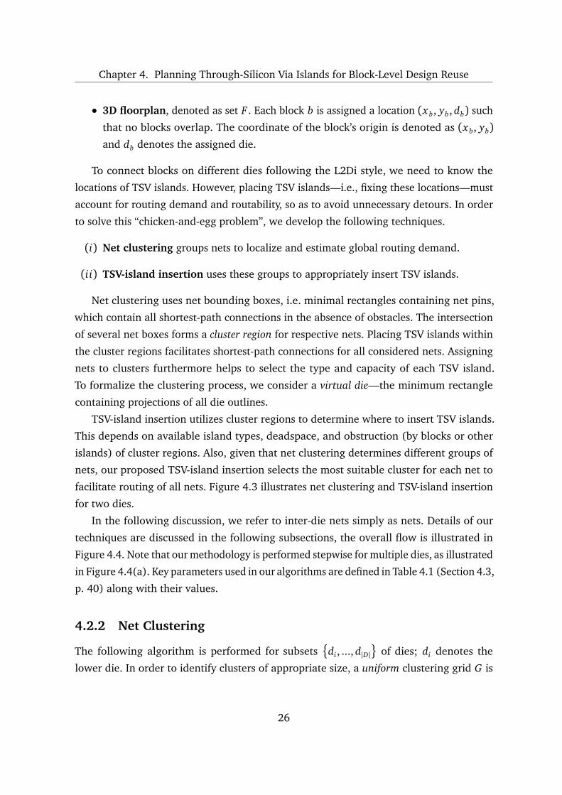
To connect blocks on different dies following the L2Di style, we need to know the
locations of TSV islands. However, placing TSV islands—i.e., fixing these locations—must
account for routing demand and routability, so as to avoid unnecessary detours. In order
to solve this “chicken-and-egg problem”, we develop the following techniques.
(i) Net clustering groups nets to localize and estimate global routing demand.
(ii) TSV-island insertion uses these groups to appropriately insert TSV islands.
Net clustering uses net bounding boxes, i.e. minimal rectangles containing net pins,
which contain all shortest-path connections in the absence of obstacles. The intersection
of several net boxes forms a cluster region for respective nets. Placing TSV islands within
the cluster regions facilitates shortest-path connections for all considered nets. Assigning
nets to clusters furthermore helps to select the type and capacity of each TSV island.
To formalize the clustering process, we consider a virtual die—the minimum rectangle
containing projections of all die outlines.
TSV-island insertion utilizes cluster regions to determine where to insert TSV islands.
This depends on available island types, deadspace, and obstruction (by blocks or other
islands) of cluster regions. Also, given that net clustering determines different groups of
nets, our proposed TSV-island insertion selects the most suitable cluster for each net to
facilitate routing of all nets. Figure 4.3 illustrates net clustering and TSV-island insertion
for two dies.
In the following discussion, we refer to inter-die nets simply as nets. Details of our
techniques are discussed in the following subsections, the overall flow is illustrated in
Figure 4.4. Note that our methodology is performed stepwise for multiple dies, as illustrated
in Figure 4.4(a). Key parameters used in our algorithms are defined in Table 4.1 (Section 4.3,
p. 40) along with their values.
4.2.2 Net Clustering
The following algorithm is performed for subsets
di, ..., d|D|
of dies; di denotes the
lower die. In order to identify clusters of appropriate size, a uniform clustering grid G is
26
Chapter 4. Planning Through-Silicon Via Islands for Block-Level Design Reuse
b2
b3
b4
b1 p1
p2p3
p4p5
p6
p'1p'2p'3
p'4
p'5p'6
c2(n2,n3)
c3(n1,n2,n3)
c1(n1,n3)
c3
n1=p1,p5n2=p2,p4n3=p3,p6
(a) (b) (c)
Figure 4.3: Net clustering and TSV-island insertion. (a) Exemplary inter-die nets n1, n2
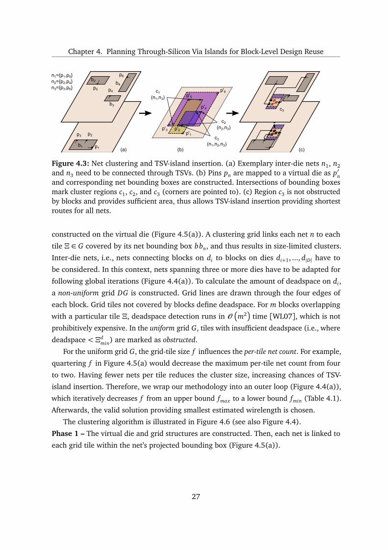
and n3 need to be connected through TSVs. (b) Pins pn are mapped to a virtual die as p′nand corresponding net bounding boxes are constructed. Intersections of bounding boxesmark cluster regions c1, c2, and c3 (corners are pointed to). (c) Region c3 is not obstructedby blocks and provides sufficient area, thus allows TSV-island insertion providing shortestroutes for all nets.
constructed on the virtual die (Figure 4.5(a)). A clustering grid links each net n to each
tile Ξ ∈ G covered by its net bounding box bbn, and thus results in size-limited clusters.
Inter-die nets, i.e., nets connecting blocks on di to blocks on dies di+1, ..., d|D| have to
be considered. In this context, nets spanning three or more dies have to be adapted for
following global iterations (Figure 4.4(a)). To calculate the amount of deadspace on di,
a non-uniform grid DG is constructed. Grid lines are drawn through the four edges of
each block. Grid tiles not covered by blocks define deadspace. For m blocks overlapping
with a particular tile Ξ, deadspace detection runs in O
m2
time [WL07], which is not
prohibitively expensive. In the uniform grid G, tiles with insufficient deadspace (i.e., where
deadspace < Ξdmin) are marked as obstructed.
For the uniform grid G, the grid-tile size f influences the per-tile net count. For example,
quartering f in Figure 4.5(a) would decrease the maximum per-tile net count from four
to two. Having fewer nets per tile reduces the cluster size, increasing chances of TSV-
island insertion. Therefore, we wrap our methodology into an outer loop (Figure 4.4(a)),
which iteratively decreases f from an upper bound fmax to a lower bound fmin (Table 4.1).
Afterwards, the valid solution providing smallest estimated wirelength is chosen.
The clustering algorithm is illustrated in Figure 4.6 (see also Figure 4.4).
Phase 1 – The virtual die and grid structures are constructed. Then, each net is linked to
each grid tile within the net’s projected bounding box (Figure 4.5(a)).
27

Chapter 4. Planning Through-Silicon Via Islands for Block-Level Design Reuse
Initializing vir tual die,Initializing gr ids
All nets connected?
TSV is land inserted?no
yes
yesno
Smalle r clusteravailable?
no
yes
Net
clu
ster
ing
Phase 1
Analyzing tiles,Determining cluster
Phase 2
Determiningdeadspace for clusters
Phase 3
Assigning netsto clusters
Phase 5
Sorting nets bydeadspace
Phase 4
Inserting TSV islandfor a largest cluster
Phase 6
TSV
-isla
nd in
sert
ion
Continue withnext iteration
(b)
(a)
3D floorplanw/o TSV islands
3D floorplanw/TSV is lands
Net clustering (di,...,d|D|) &TSV-island insertion (di)
i = i+1
i == |D| - 1 ?
|D| dies;index i = 0
no
yes
clustering-tilesize f = fmax f = f - 1
f < fmin ?
no
yes
Store solution
Apply bestsolution for di
Figure 4.4: L2Di integration flow. (a) Given a 3D floorplan, global iterations start withthe lowest die and perform net clustering and TSV-island insertion stepwise for all dies.Best solutions refer to solutions where inserted TSV islands result in smallest estimatedwirelength. (b) Details on net clustering and TSV-island insertion. First, net clusteringlocalizes global routing demand while determining cluster regions. Second, TSV-islandinsertion into cluster regions is stepwise conducted.
28
Chapter 4. Planning Through-Silicon Via Islands for Block-Level Design Reuse
1.0 0.44 0.73 1.0
(0,0) (1,0) (2,0) (3,0)
(0,0)
(0,1)
(0,2)
(0,3)
(0,0) (1,0) (2,0) (3,0)
(0,0)
(0,1)
(0,2)
(0,3) b1
b2b4
b3bbn1
bbn2
bbn3
bbn4
(a) (b)
Figure 4.5: Grid structures. (a) The uniform clustering grid G on the virtual die. Accordingto projected bounding boxes, we link nets to covered tiles. (b) In order to determinedeadspace, a non-uniform grid DG is constructed on the die (overlapped with G only forillustration purpose). The per-tile ratio of deadspace is determined and back-annotated toG, as illustrated in the last row.
Phase 2 – For each unobstructed grid tile the largest cluster is determined in procedure
DE T E R M I N E _CL U S T E R—each linked net is considered as long as the resulting inter-
section of bounding boxes is non-empty.3 Moreover, we impose a lower bound Ωmin on
the overlap area between the intersection and tiles, in order to assure the intersection is
covering the unobstructed tile to some minimal degree and to maintain a minimal cluster
size. An upper bound Onets of nets assigned to each cluster c must not be exceeded. Each
net n can be associated with at most Ol ink clusters. We note that intersections in general
can overlap more than one tile, depending on the bounding boxes. Therefore, we allow
cluster regions to be extended within procedure UP D AT E_C L U S T E R_RE G I O N in cases
where clusters are spread across several tiles. Next, we attempt to cluster yet-unclustered
nets in procedure D E T E R M I N E_F U R T H E R_C L U S T E R; nets are considered for clustering
independent of related tiles, thus several combinations of nets are resulting. Besides that,
clustering is performed as described for procedure DE T E R M I N E _CL U S T E R. This step
allows one-net clusters; all nets are thus clustered afterwards.
Phase 3 – Available deadspace is determined for each cluster region. It is summed up over
available deadspace of related grid tiles while considering the particular intersection of
the cluster region and tile.
3For example, consider the second row from top of the clustering grid in Figure 4.5(a). Note that tiles(0, 2) and (3, 2) are not used for cluster determination, since they are obstructed (Figure 4.5(b)). Clusteringfor tile (1,2) results in c1 with c1.nets =
n1, n2, n4
, and for tile (2, 2) in c2 with c2.nets =
n2, n4
.
29

Chapter 4. Planning Through-Silicon Via Islands for Block-Level Design Reuse
1: IN I T I A L I Z E _V I R T U A L _D I E
li , ..., l|L|
▷ Phase 1: initialize virtual die and grids2: G← CO N S T R U C T_C L U S T E R I N G _GR I D
li , ..., l|L|, N , B, F
3: D← CO N S T R U C T _DE A D S PA C E _GR I D(li , B, F)4: DE T E R M I N E _DE A D S PA C E(D, G) ▷ Phase 1: determine deadspace; mark tiles Ξ ∈ G where
deadspace is < Ξdmin as obstructed
5: for each net n ∈ N where n connects li and li+1, ..., l|L| do ▷ Phase 1: link nets to tiles6: bbn← DE T E R M I N E _B O U N D I N G_B O X(n, B, F)7: for each grid tile Ξ ∈ G where Ξ is covered by bbn do8: append n to Ξ.nets9: end for
10: end for11: for each grid tile Ξ ∈ G where Ξ.obst ructed == false do ▷ Phase 2: determine clusters12: c← DE T E R M I N E _C L U S T E R(Ξ,Ωmin, Onets, Ol ink)13: if c /∈ C then14: insert c into C15: for each net n ∈ c.nets do16: n.clustered = true17: end for18: else if |c.nets|> 0 then19: UP D AT E _C L U S T E R_RE G I O N(c,Ξ)20: end if21: end for22: progress = true ▷ Phase 2: handle yet unclustered nets23: while progress == true do24: RE S E T(unclustered_nets)25: for each net n ∈ N where n.clustered == false do26: append n to unclustered_nets27: end for28: c← DE T E R M I N E _FU R T H E R _C L U S T E R(unclustered_nets)29: progress = (c /∈ C)30: if progress == true then31: insert c into C32: for each net n ∈ c.nets do33: n.clustered = true34: end for35: end if36: end while37: for each cluster c ∈ C do ▷ Phase 3: determine available deadspace38: for each grid tile Ξ ∈ G where Ξ is covered by c.bb do39: c.deadspace+ =IN T E R S E C T I O N(c.bb,Ξ)×Ξ.deadspace40: end for41: end for
Figure 4.6: Net clustering algorithm. Input data are described in Subsection 4.2.1.
30
Chapter 4. Planning Through-Silicon Via Islands for Block-Level Design Reuse
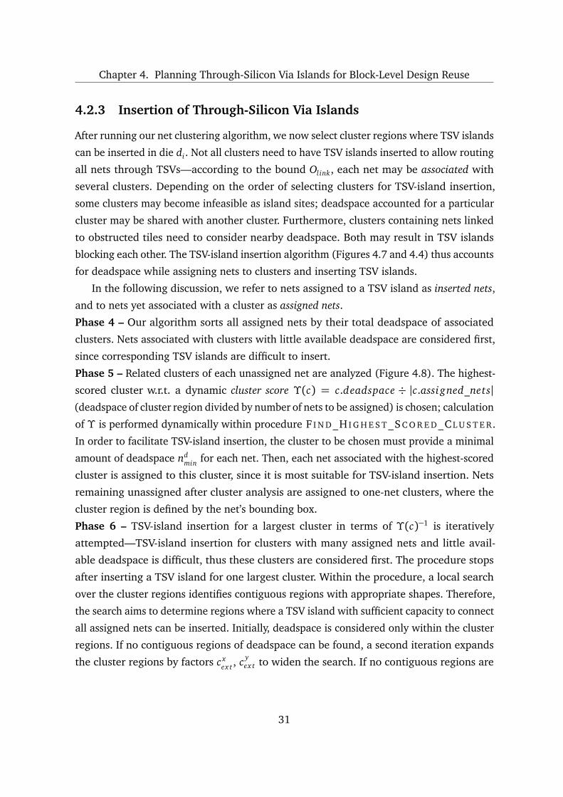
4.2.3 Insertion of Through-Silicon Via Islands
After running our net clustering algorithm, we now select cluster regions where TSV islands
can be inserted in die di. Not all clusters need to have TSV islands inserted to allow routing
all nets through TSVs—according to the bound Ol ink, each net may be associated with
several clusters. Depending on the order of selecting clusters for TSV-island insertion,
some clusters may become infeasible as island sites; deadspace accounted for a particular
cluster may be shared with another cluster. Furthermore, clusters containing nets linked
to obstructed tiles need to consider nearby deadspace. Both may result in TSV islands
blocking each other. The TSV-island insertion algorithm (Figures 4.7 and 4.4) thus accounts
for deadspace while assigning nets to clusters and inserting TSV islands.
In the following discussion, we refer to nets assigned to a TSV island as inserted nets,
and to nets yet associated with a cluster as assigned nets.
Phase 4 – Our algorithm sorts all assigned nets by their total deadspace of associated
clusters. Nets associated with clusters with little available deadspace are considered first,
since corresponding TSV islands are difficult to insert.
Phase 5 – Related clusters of each unassigned net are analyzed (Figure 4.8). The highest-
scored cluster w.r.t. a dynamic cluster score Υ (c) = c.deadspace ÷ |c.assi gned_nets|(deadspace of cluster region divided by number of nets to be assigned) is chosen; calculation
of Υ is performed dynamically within procedure F I N D_H I G H E S T _S C O R E D_C L U S T E R.
In order to facilitate TSV-island insertion, the cluster to be chosen must provide a minimal
amount of deadspace ndmin for each net. Then, each net associated with the highest-scored
cluster is assigned to this cluster, since it is most suitable for TSV-island insertion. Nets
remaining unassigned after cluster analysis are assigned to one-net clusters, where the
cluster region is defined by the net’s bounding box.
Phase 6 – TSV-island insertion for a largest cluster in terms of Υ (c)−1 is iteratively
attempted—TSV-island insertion for clusters with many assigned nets and little avail-
able deadspace is difficult, thus these clusters are considered first. The procedure stops
after inserting a TSV island for one largest cluster. Within the procedure, a local search
over the cluster regions identifies contiguous regions with appropriate shapes. Therefore,
the search aims to determine regions where a TSV island with sufficient capacity to connect
all assigned nets can be inserted. Initially, deadspace is considered only within the cluster
regions. If no contiguous regions of deadspace can be found, a second iteration expands
the cluster regions by factors c xex t , c y
ex t to widen the search. If no contiguous regions are
31

Chapter 4. Planning Through-Silicon Via Islands for Block-Level Design Reuse
1: SO R T _NE T S_BY _AR E A _SU P P LY(N, C) ▷ Phase 4: sort nets2: progress = true3: while progress == true do4: for each net n ∈ N where n.inser ted == false do ▷ Phase 5: assign nets5: c← F I N D_H I G H E S T _SC O R E D_C L U S T E R
n, C , ndmin
6: for each net m ∈ c.nets do7: append m to c.assi gned_nets8: end for9: end for
10: (c, t)← IN S E R T _TSV_IS L A N D(li, C , T ) ▷ Phase 6: iteratively insert TSV islandfor a largest cluster
11: progress = (c!= null)12: if progress == true then ▷ Phase 6: mark inserted nets13: for each net n ∈ N where n ∈ c.nets do14: n.inser ted = true15: n.TSV_island ← t16: if n connects to layers li+2, ..., l|L| then ▷ Phase 6: adapt pins for nets
spanning ≥ 3 layers17: n.pin (li+1)← t.center18: end if19: end for20: MA R K _C L U S T E R_HA N D L E D(c)21: for each cluster c ∈ C do ▷ Phase 6: remove all net assignments22: reset c.assi gned_nets23: end for24: end if25: end while
Figure 4.7: TSV-island insertion algorithm. Input data are described in Subsection 4.2.1.
32
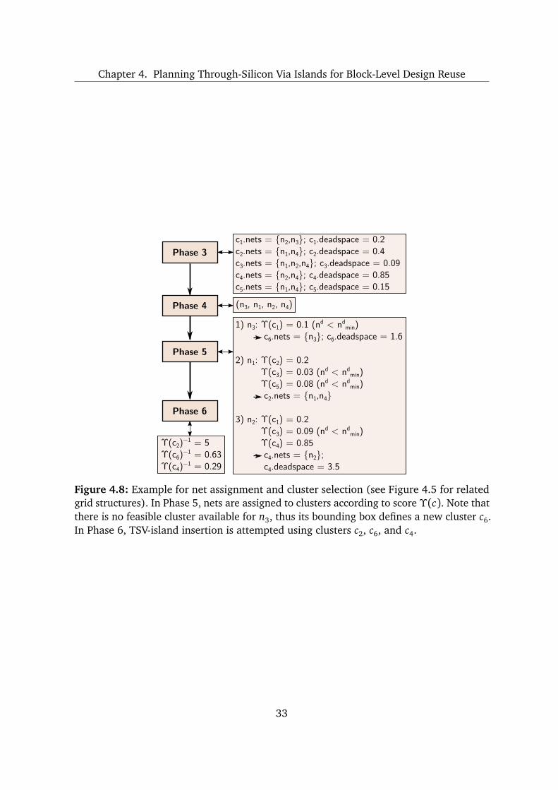
Chapter 4. Planning Through-Silicon Via Islands for Block-Level Design Reuse
Phase 4
c1.nets = n2,n3; c1.deadspace = 0.2c2.nets = n1,n4; c2.deadspace = 0.4c3.nets = n1,n2,n4; c3.deadspace = 0.09c4.nets = n2,n4; c4.deadspace = 0.85c5.nets = n1,n4; c5.deadspace = 0.15
(n3, n1, n2, n4)
Phase 5
Phase 3
1) n3: Υ(c1) = 0.1 (nd < ndmin)
c6.nets = n3; c6.deadspace = 1.6
2) n1: Υ(c2) = 0.2 Υ(c3) = 0.03 (nd < nd
min) Υ(c5) = 0.08 (nd < nd
min) c2.nets = n1,n4
3) n2: Υ(c1) = 0.2 Υ(c3) = 0.09 (nd < nd
min) Υ(c4) = 0.85 c4.nets = n2; c4.deadspace = 3.5
Phase 6
Υ(c2)−1 = 5Υ(c6)−1 = 0.63Υ(c4)−1 = 0.29
Figure 4.8: Example for net assignment and cluster selection (see Figure 4.5 for relatedgrid structures). In Phase 5, nets are assigned to clusters according to score Υ (c). Note thatthere is no feasible cluster available for n3, thus its bounding box defines a new cluster c6.In Phase 6, TSV-island insertion is attempted using clusters c2, c6, and c4.
33

Chapter 4. Planning Through-Silicon Via Islands for Block-Level Design Reuse
found again for any cluster, block shifting or deadspace-channel insertion can be performed
to increase deadspace (Subsection 4.2.4). Therefore, the cluster providing the maximum
amount of deadspace is chosen first to minimize the amount of required shifting. After
successful TSV-island insertion, inserted nets are marked as handled, and all non-inserted
nets are unassigned from remaining clusters—according to Υ , each non-inserted net may
be assigned to different clusters now. Furthermore, inserted nets connecting blocks on die
di to blocks on dies di+2, ..., d|D| (i.e., spanning three or more dies) have to be adapted. The
center of each related TSV island defines a virtual net pin, which is considered as respective
net pin for following net-clustering iterations. Iterations continue with Phase 5 until all nets
are inserted. If TSV-island insertion fails for all available clusters, our algorithm terminates
with no solution.
4.2.4 Deadspace Insertion and Redistribution
TSV-island insertion can fail because deadspace is unavailable where it is needed. To
address these failures, we propose two techniques to insert and redistribute deadspace.
(i) Deadspace-channel insertion provides regions to insert TSV islands, mainly in
cases of too compact floorplans (Figure 4.9).
(ii) Block shifting allows to redistribute available deadspace to facilitate TSV-island
insertion (Figure 4.10).
Deadspace-channel insertion is often applied in industrial chip designs to facilitate
routing, and to enable placement of buffers and glue logic. Trivially, it would also increase
flexibility of TSV-island insertion. However, this is less appropriate for compact floorplans.
Block shifting, on the other hand, facilitates compact floorplans, where outlines are
maintained. This approach is more complex, and success in gaining a sufficient amount of
continuous deadspace is dependent on the actual floorplan. We develop two block-shifting
techniques that rely on similar baseline algorithms: initial shifting and iterative shifting
(Figure 4.11). Initial shifting performs block shifting once before our methodology is
applied, as explained later on. Iterative shifting is performed during TSV-island insertion
(IN S E R T _TSV_IS L A N D, Figure 4.7) when necessary.
The algorithm for block shifting is based on the concept of spatial slack in floorplan-
ning [AM02] and performs analysis of cluster regions. Slacks, for x- and y-dimension,
describe maximal possible displacements of a block within the floorplan outline. When
34
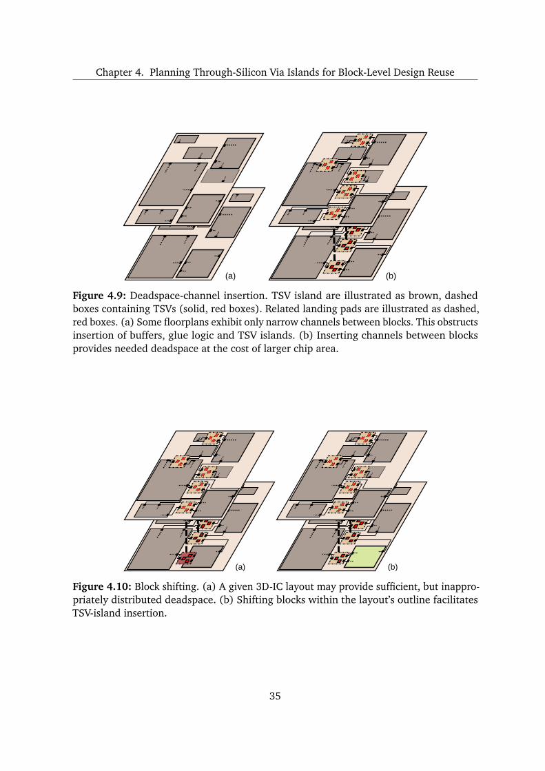
Chapter 4. Planning Through-Silicon Via Islands for Block-Level Design Reuse
M'
(a) (b)
M'
Figure 4.9: Deadspace-channel insertion. TSV island are illustrated as brown, dashedboxes containing TSVs (solid, red boxes). Related landing pads are illustrated as dashed,red boxes. (a) Some floorplans exhibit only narrow channels between blocks. This obstructsinsertion of buffers, glue logic and TSV islands. (b) Inserting channels between blocksprovides needed deadspace at the cost of larger chip area.
M' M'
(a) (b)
Figure 4.10: Block shifting. (a) A given 3D-IC layout may provide sufficient, but inappro-priately distributed deadspace. (b) Shifting blocks within the layout’s outline facilitatesTSV-island insertion.
35
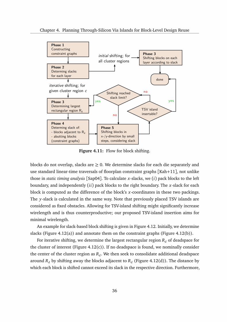
Chapter 4. Planning Through-Silicon Via Islands for Block-Level Design Reuse
Constructingconstraint graphs
Phase 1
Determing slacksfor each layer
Phase 2
initial shifting; forall cluster regions
Shifting blocks on eachlayer according to slack
Phase 3
iterative shifting; forgiven cluster region c
Determining largestrectangular region Rd
Phase 3
Determing slack of:- blocks adjacent to Rd- abutting blocks(constraint graphs)
Phase 4
Shifting blocks inx-/y-direction by smallsteps, considering slack
Phase 5
TSV islandinsertable?
Shifting reachedslack limit?
done
yes
no
yes
no
Figure 4.11: Flow for block shifting.
blocks do not overlap, slacks are ≥ 0. We determine slacks for each die separately and
use standard linear-time traversals of floorplan constraint graphs [Kah+11], not unlike
those in static timing analysis [Sap04]. To calculate x-slacks, we (i) pack blocks to the left
boundary, and independently (ii) pack blocks to the right boundary. The x-slack for each
block is computed as the difference of the block’s x-coordinates in these two packings.
The y-slack is calculated in the same way. Note that previously placed TSV islands are
considered as fixed obstacles. Allowing for TSV-island shifting might significantly increase
wirelength and is thus counterproductive; our proposed TSV-island insertion aims for
minimal wirelength.
An example for slack-based block shifting is given in Figure 4.12. Initially, we determine
slacks (Figure 4.12(a)) and annotate them on the constraint graphs (Figure 4.12(b)).
For iterative shifting, we determine the largest rectangular region Rd of deadspace for
the cluster of interest (Figure 4.12(c)). If no deadspace is found, we nominally consider
the center of the cluster region as Rd . We then seek to consolidate additional deadspace
around Rd by shifting away the blocks adjacent to Rd (Figure 4.12(d)). The distance by
which each block is shifted cannot exceed its slack in the respective direction. Furthermore,
36
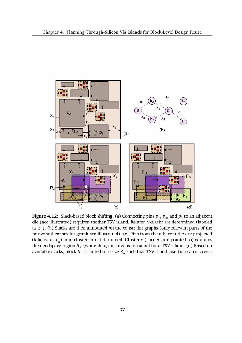
Chapter 4. Planning Through-Silicon Via Islands for Block-Level Design Reuse
(a)
(c) (d)
(b)p3 b1
b2
b3
x1
x3x4
x6
x2
p1p2
p3
p'4p'5
p'6
p1p2
p1p2
p3
p'4p'5
p'6
Rd
b1 b1
b2b2
b2b3
b2b1
b2t1
b2s
b2t2
x5
x1
x3 x4
x2
x5x6
c
Figure 4.12: Slack-based block shifting. (a) Connecting pins p1, p2, and p3 to an adjacentdie (not illustrated) requires another TSV island. Related x-slacks are determined (labeledas xn). (b) Slacks are then annotated on the constraint graphs (only relevant parts of thehorizontal constraint graph are illustrated). (c) Pins from the adjacent die are projected(labeled as p′n), and clusters are determined. Cluster c (corners are pointed to) containsthe deadspace region Rd (white dots); its area is too small for a TSV island. (d) Based onavailable slacks, block b1 is shifted to resize Rd such that TSV-island insertion can succeed.
37
Chapter 4. Planning Through-Silicon Via Islands for Block-Level Design Reuse
the sum of such displacements in each direction cannot exceed the floorplan slack, i.e., the
largest slack of any one block. Shifting a block may require shifting its abutting neighbors
and other blocks. To this end, we maintain the floorplan configuration using constraint
graphs. If Rd cannot be increased sufficiently, we choose another region of deadspace
within the cluster region.
For initial shifting, we independently determine available slacks of blocks on all dies and
shift blocks such that they are centered according to slacks. This may facilitate TSV-island
insertion around blocks—they are likely to be distributed towards the center of the die
afterwards, with deadspace around them.
4.3 Experimental Investigation
In this section, we initially describe our approach for estimating wirelengths as well as
the configuration for our experiments. Then, we discuss results for L2Di integration and
related experiments.
4.3.1 Wirelength Estimation
Tsai et al. [TWH11] show that using TSVs not only affects the final wirelength, but may also
decrease the accuracy of wirelength estimation during floorplanning, if not appropriately
addressed. As mentioned in Chapter 2, previous work on 3D integration ignores TSV
footprints and locations in some cases. Subsequently, TSV placement is likely to be hindered
due to inappropriately distributed deadspace. Therefore, the well-known metric half-
perimeter wirelength (HPWL) may be insufficient for estimating wirelength of 3D ICs.
Note that this estimation metric, however, provides a reference value for optimal TSV
insertion. We refer to it as NBB-3D-HPWL (Figure 4.13(a)). Tsai et al. [TWH11] extend it
by considering TSV locations during bounding-box construction; we refer to this technique
as BB-3D-HPWL (Figure 4.13(b)). However, Tsai et al. neglect that using TSVs implies
connecting blocks to TSV landing pads on associated dies. To estimate resulting wirelength
more precisely, Kim et al. [KAL09] introduce net splitting, i.e., they construct bounding
boxes on each die separately and sum up resulting HPWLs. We refer to this technique
as BB-2D3D-HPWL (Figure 4.13(c)); it is applied in our experiments described in the
remainder of this section.
38
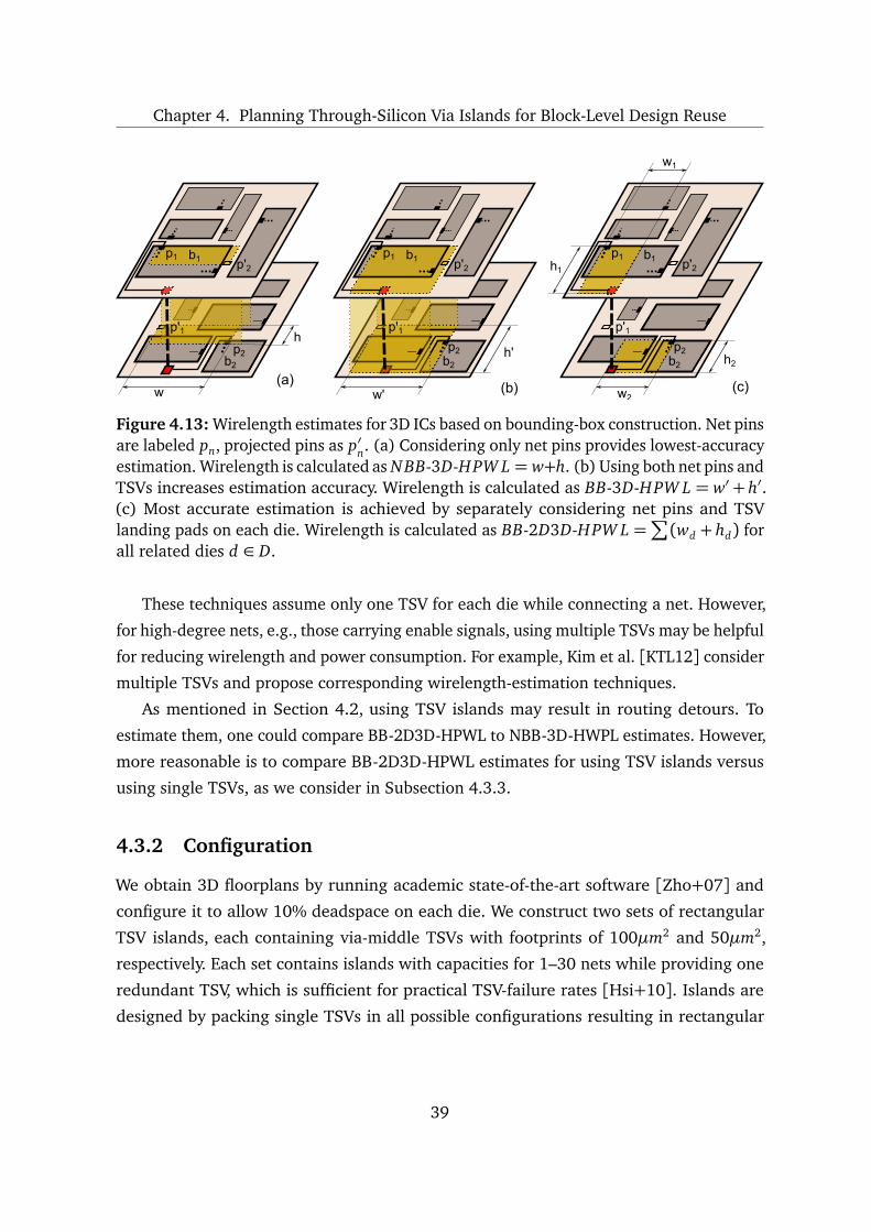
Chapter 4. Planning Through-Silicon Via Islands for Block-Level Design Reuse
(a)(b) (c)
b2p2
p'1
b2p2
p'1
w
h
w'
h'b2p2
p'1
w2
h2
b1p1p'2
b1p1p'2
b1p1p'2h1
w1
Figure 4.13: Wirelength estimates for 3D ICs based on bounding-box construction. Net pinsare labeled pn, projected pins as p′n. (a) Considering only net pins provides lowest-accuracyestimation. Wirelength is calculated as NBB-3D-HPW L = w+h. (b) Using both net pins andTSVs increases estimation accuracy. Wirelength is calculated as BB-3D-HPW L = w′ + h′.(c) Most accurate estimation is achieved by separately considering net pins and TSVlanding pads on each die. Wirelength is calculated as BB-2D3D-HPW L =
(wd + hd) forall related dies d ∈ D.
These techniques assume only one TSV for each die while connecting a net. However,
for high-degree nets, e.g., those carrying enable signals, using multiple TSVs may be helpful
for reducing wirelength and power consumption. For example, Kim et al. [KTL12] consider
multiple TSVs and propose corresponding wirelength-estimation techniques.
As mentioned in Section 4.2, using TSV islands may result in routing detours. To
estimate them, one could compare BB-2D3D-HPWL to NBB-3D-HWPL estimates. However,
more reasonable is to compare BB-2D3D-HPWL estimates for using TSV islands versus
using single TSVs, as we consider in Subsection 4.3.3.
4.3.2 Configuration
We obtain 3D floorplans by running academic state-of-the-art software [Zho+07] and
configure it to allow 10% deadspace on each die. We construct two sets of rectangular
TSV islands, each containing via-middle TSVs with footprints of 100µm2 and 50µm2,
respectively. Each set contains islands with capacities for 1–30 nets while providing one
redundant TSV, which is sufficient for practical TSV-failure rates [Hsi+10]. Islands are
designed by packing single TSVs in all possible configurations resulting in rectangular
39
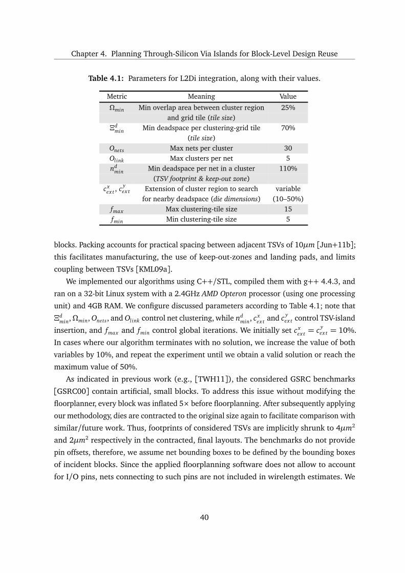
Chapter 4. Planning Through-Silicon Via Islands for Block-Level Design Reuse
Table 4.1: Parameters for L2Di integration, along with their values.
Metric Meaning Value
Ωmin Min overlap area between cluster region 25%and grid tile (tile size)
Ξdmin Min deadspace per clustering-grid tile 70%
(tile size)Onets Max nets per cluster 30Ol ink Max clusters per net 5nd
min Min deadspace per net in a cluster 110%(TSV footprint & keep-out zone)
c xex t , c y
ex t Extension of cluster region to search variablefor nearby deadspace (die dimensions) (10–50%)
fmax Max clustering-tile size 15fmin Min clustering-tile size 5
blocks. Packing accounts for practical spacing between adjacent TSVs of 10µm [Jun+11b];this facilitates manufacturing, the use of keep-out-zones and landing pads, and limits
coupling between TSVs [KML09a].We implemented our algorithms using C++/STL, compiled them with g++ 4.4.3, and
ran on a 32-bit Linux system with a 2.4GHz AMD Opteron processor (using one processing
unit) and 4GB RAM. We configure discussed parameters according to Table 4.1; note that
Ξdmin,Ωmin, Onets, and Ol ink control net clustering, while nd
min, c xex t and c y
ex t control TSV-island
insertion, and fmax and fmin control global iterations. We initially set c xex t = c y
ex t = 10%.
In cases where our algorithm terminates with no solution, we increase the value of both
variables by 10%, and repeat the experiment until we obtain a valid solution or reach the
maximum value of 50%.
As indicated in previous work (e.g., [TWH11]), the considered GSRC benchmarks
[GSRC00] contain artificial, small blocks. To address this issue without modifying the
floorplanner, every block was inflated 5× before floorplanning. After subsequently applying
our methodology, dies are contracted to the original size again to facilitate comparison with
similar/future work. Thus, footprints of considered TSVs are implicitly shrunk to 4µm2
and 2µm2 respectively in the contracted, final layouts. The benchmarks do not provide
pin offsets, therefore, we assume net bounding boxes to be defined by the bounding boxes
of incident blocks. Since the applied floorplanning software does not allow to account
for I/O pins, nets connecting to such pins are not included in wirelength estimates. We
40

Chapter 4. Planning Through-Silicon Via Islands for Block-Level Design Reuse
consider intra-die nets by summing up the HPWL of their bounding box and include them
in wirelength estimates. Since we do not perform net assignment to particular TSVs within
islands, reported wirelength estimates consider the center of TSV islands to determine
bounding boxes, resulting in presumably pessimistic wirelength estimates. We also report
runtime for our algorithms (summed up for global iterations), TSV count, and the area of
the final layouts, which is defined as the product of the maximum height and maximum
width over all dies.
We consider two design configurations; one with guaranteed channels, one without
channels.4 To insert channels between the blocks without modifying the floorplanner, every
block was inflated (by 5%) before floorplanning and contracted to the original size after
floorplanning. However, this increases floorplan area (by 10.25%).
4.3.3 Results and Discussion
As mentioned in Subsection 4.2.2, our methodology is wrapped into a loop which iteratively
decreases the grid-tile size f from an upper bound fmax to a lower bound fmin (Table 4.1).
Figure 4.14 indicates that the density of valid solutions may increase with decreasing tile
size. Small tiles limit the per-tile net count, thus also limit the cluster size. In practice,
smaller tiles lead to fewer nets being assigned per cluster, larger cluster regions and
easier TSV-island insertion. This also reduces wirelength, as expected. However, there is a
lower bound for these relations; very small tiles result in many clusters with few assigned
nets, thus many small TSV islands are inserted. Since placed TSV islands represent fixed
obstacles, this may complicate iterative block shifting. Also, our local search over cluster
regions identifies contiguous deadspace regions for TSV-island insertion in a greedy manner.
Therefore, determining appropriate regions for clusters considered late during TSV-island
insertion is more likely to fail; there are already many TSV islands spread out within
deadspace regions. After confirming these trends in different experimental configurations,
we set global iteration variables fmax = 15 and fmin = 5.
Table 4.2 reports results on GSRC benchmarks [GSRC00], which are discussed next.
First, we evaluate our techniques for deadspace insertion and redistribution. Recall
that deadspace-channel insertion increases floorplan’s deadspace by inflating blocks and
4Traditional algorithms for floorplanning pack blocks without channels. However, many industry designsaccount for channels between blocks to facilitate gate sizing or insertion of buffers and/or additional,interconnecting logic.
41
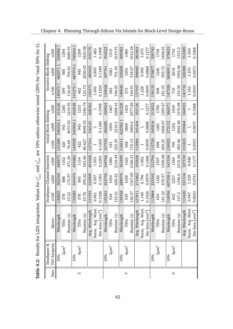
Chapter 4. Planning Through-Silicon Via Islands for Block-Level Design ReuseTa
ble
4.2:
Resu
lts
for
L2D
iint
egra
tion
.Val
ues
for
cx ext
and
cy ext
are
10%
unle
ssot
herw
ise
note
d(2
0%fo
r†a
nd50
%fo
r‡)
.
Dea
dspa
ce&
Dea
dspa
ce-C
hann
elIn
sert
ion
Init
ialB
lock
Shif
ting
Iter
ativ
eB
lock
Shif
ting
Die
sTS
Vfo
otpr
int
Met
ric
n100
n200
n300
n100
n200
n300
n100
n200
n300
2
10%
Wir
elen
gth
1308
2530
2344
4469
7313
1589
5403
24‡
4141
2614
9473
†48
2071
‡53
0096
†2µ
m2
TSV
s37
888
811
6242
094
112
8539
998
512
94R
unti
me
(s)
19.2
217
3.97
471.
2676
.69
4075
.93
1219
.95
118.
4979
4.63
2689
.91
10%
Wir
elen
gth
1330
8534
5474
4550
8214
3039
5439
62‡
4426
3815
1272
†48
7974
‡74
0244
‡4µ
m2
TSV
s37
889
511
5442
294
312
3340
294
512
09R
unti
me
(s)
19.7
829
5.22
503.
4686
.627
4698
.35
1346
.74
124.
7320
30.4
318
35.0
8A
vg.W
irel
engt
h13
1955
3239
0945
1028
1373
1454
2143
4283
8215
0373
4850
2363
5170
Nor
m.
Avg
.Wir
el.
0.96
10.
597
1.05
31
11
1.09
50.
895
1.48
3D
ieA
rea
mm
2
0.13
260.
1301
0.22
030.
1203
0.11
800.
1998
0.12
030.
1180
0.19
98
3
10%
Wir
elen
gth
1252
6325
4756
3497
6610
7556
2602
8532
9024
1345
6829
7761
3542
232µ
m2
TSV
s53
410
3414
8054
110
9414
6758
210
8115
19R
unti
me
(s)
123.
2162
8.22
2124
.44
222.
3922
16.5
3268
.41
146.
0570
1.43
1619
.91
10%
Wir
elen
gth
1303
5828
8970
3618
9011
6611
4225
82‡
3812
2814
0626
3202
0840
9382
4µm
2TS
Vs
539
1038
1425
568
3809
1455
573
1055
1485
Run
tim
e(s
)12
6.37
1167
.69
2166
.21
172.
1334
04.6
2977
.85
144.
9151
8.07
1612
.56
Avg
.Wir
elen
gth
1278
1127
1863
3558
2811
2084
3414
3435
5126
1375
9730
8985
3818
03N
orm
.A
vg.W
irel
.1.
140
0.79
61.
002
11
11.
228
0.90
51.
075
Die
Are
a
mm
2
0.10
360.
0979
0.14
080.
0939
0.08
880.
1277
0.09
390.
0888
0.12
77
4
10%
Wir
elen
gth
1138
8423
5542
3127
6411
2720
2458
1631
3033
1361
3527
0877
3297
452µ
m2
TSV
s65
411
8215
9769
612
8117
0069
812
4617
58R
unti
me
(s)
141.
2267
0.97
1590
.08
269.
2516
08.0
712
95.6
718
1.35
593.
7214
58.0
110
%W
irel
engt
h11
6956
4075
26‡
3415
3613
0925
2731
1236
6571
1473
2836
9895
‡37
6833
4µm
2TS
Vs
652
2257
1569
705
1252
1659
719
2018
1710
Run
tim
e(s
)14
7.2
1346
.623
16.3
638
3.66
2692
.46
1576
.98
154.
3619
92.4
614
15.2
Avg
.Wir
elen
gth
1154
2032
1534
3271
5012
1823
2594
6434
4933
1417
3232
0386
3532
89N
orm
.A
vg.W
irel
.0.
947
1.23
90.
948
11
11.
163
1.23
51.
024
Die
Are
a
mm
2
0.06
530.
0741
0.11
770.
0593
0.06
730.
1068
0.05
930.
0673
0.10
68
42
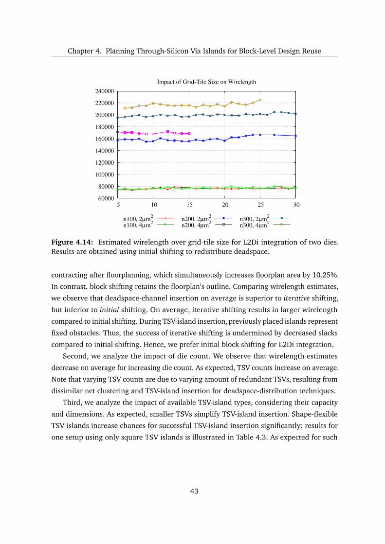
Chapter 4. Planning Through-Silicon Via Islands for Block-Level Design Reuse
60000
80000
100000
120000
140000
160000
180000
200000
220000
240000
5 10 15 20 25 30
Impact of Grid-Tile Size on Wirelength
n100, 2µm2
n100, 4µm2n200, 2µm2
n200, 4µm2n300, 2µm2
n300, 4µm2
Figure 4.14: Estimated wirelength over grid-tile size for L2Di integration of two dies.Results are obtained using initial shifting to redistribute deadspace.
contracting after floorplanning, which simultaneously increases floorplan area by 10.25%.
In contrast, block shifting retains the floorplan’s outline. Comparing wirelength estimates,
we observe that deadspace-channel insertion on average is superior to iterative shifting,
but inferior to initial shifting. On average, iterative shifting results in larger wirelength
compared to initial shifting. During TSV-island insertion, previously placed islands represent
fixed obstacles. Thus, the success of iterative shifting is undermined by decreased slacks
compared to initial shifting. Hence, we prefer initial block shifting for L2Di integration.
Second, we analyze the impact of die count. We observe that wirelength estimates
decrease on average for increasing die count. As expected, TSV counts increase on average.
Note that varying TSV counts are due to varying amount of redundant TSVs, resulting from
dissimilar net clustering and TSV-island insertion for deadspace-distribution techniques.
Third, we analyze the impact of available TSV-island types, considering their capacity
and dimensions. As expected, smaller TSVs simplify TSV-island insertion. Shape-flexible
TSV islands increase chances for successful TSV-island insertion significantly; results for
one setup using only square TSV islands is illustrated in Table 4.3. As expected for such
43
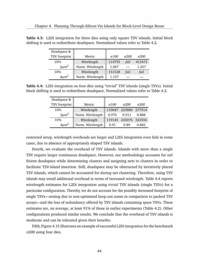
Chapter 4. Planning Through-Silicon Via Islands for Block-Level Design Reuse
Table 4.3: L2Di integration for three dies using only square TSV islands. Initial blockshifting is used to redistribute deadspace. Normalized values refer to Table 4.2.
Deadspace &TSV footprint Metric n100 n200 n300
10% Wirelength 114795 fail 4134722µm2 Norm. Wirelength 1.067 — 1.257
10% Wirelength 151528 fail fail4µm2 Norm. Wirelength 1.157 — —
Table 4.4: L2Di integration on four dies using “trivial” TSV islands (single TSVs). Initialblock shifting is used to redistribute deadspace. Normalized values refer to Table 4.2.
Deadspace &TSV footprint Metric n100 n200 n300
10% Wirelength 110047 223880 2779142µm2 Norm. Wirelength 0.976 0.911 0.888
10% Wirelength 119145 243076 3235564µm2 Norm. Wirelength 0.91 0.89 0.882
restricted setup, wirelength overheads are larger and L2Di integration even fails in some
cases, due to absence of appropriately shaped TSV islands.
Fourth, we evaluate the overhead of TSV islands. Islands with more than a single
TSV require larger continuous deadspace. However, our methodology accounts for suf-
ficient deadspace while determining clusters and assigning nets to clusters in order to
facilitate TSV-island insertion. Still, deadspace may be obstructed by iteratively placed
TSV islands, which cannot be accounted for during net clustering. Therefore, using TSV
islands may entail additional overhead in terms of increased wirelength. Table 4.4 reports
wirelength estimates for L2Di integration using trivial TSV islands (single TSVs) for a
particular configuration. Thereby, we do not account for the possibly increased footprint of
single TSVs—arising due to non-optimized keep-out-zones in comparison to packed TSV
arrays—and the loss of redundancy offered by TSV islands containing spare TSVs. These
estimates are, on average, at least 91% of those in earlier experiments (Table 4.2). Other
configurations produced similar results. We conclude that the overhead of TSV islands is
moderate and can be tolerated given their benefits.
Fifth, Figure 4.15 illustrates an example of successful L2Di integration for the benchmark
n200 using four dies.
44
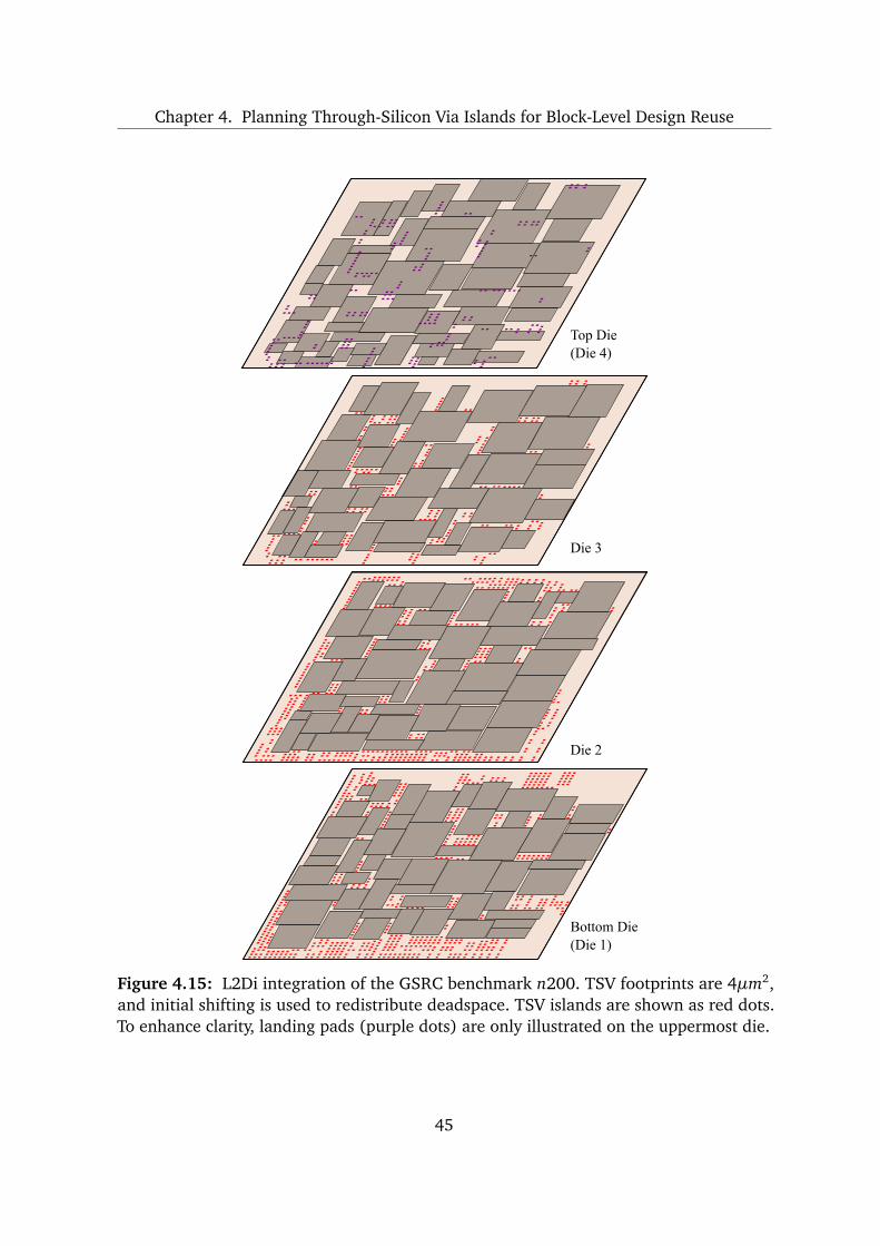
Chapter 4. Planning Through-Silicon Via Islands for Block-Level Design Reuse
Bottom Die(Die 1)
Die 2
Die 3
Top Die(Die 4)
Figure 4.15: L2Di integration of the GSRC benchmark n200. TSV footprints are 4µm2,and initial shifting is used to redistribute deadspace. TSV islands are shown as red dots.To enhance clarity, landing pads (purple dots) are only illustrated on the uppermost die.
45

Chapter 4. Planning Through-Silicon Via Islands for Block-Level Design Reuse
4.4 Summary and Conclusions
Our work presented in this chapter seeks to streamline the transition from existing practice
in 2D chip design to 3D integration. Numerous technical challenges in this transition were
pointed out in Section 2.5, as well as by industry experts, namely Borkar (Intel) [Bor11] and
Topaloglu (GLOBALFOUNDRIES) [Top11]. TSVs tend to disrupt conventional layouts and,
thereby, impact several dies at once. Manufacturing of 3D-enabled dies is complicated by
considerations of yield for TSVs and stacked dies [FRB07; Pan+12], as well as cost-effective
testing [LC09; Mar+10]. EDA tools need to support both 3D design-space exploration efforts
and comprehensive layout optimization, in particular TSV management [Lim10]. Power
delivery and thermal management are further challenges for tool development [CAD10;
CS09].The lack of commercial 3D EDA tools hinders a cost-effective transition, and even when
such tools become widely available, upgrading extensive 2D-IP portfolios for 3D integration
may take years. A key insight in our work is that many of the benefits provided by 3D ICs
can be obtained while reusing existing 2D-IP blocks. In fact, such reuse is required for
heterogeneous 3D system-on-chips where circuit modules cannot be split between memory,
digital, analog, and MEMS dies. We introduce the design style L2Di, where TSVs can be
clustered into TSV islands rather than always placed individually. This style appears most
promising and least risky for 3D-IC design in the next 5-8 years.
To enable the L2Di style, we contribute novel techniques for net clustering and TSV-
island insertion. We also develop techniques to insert and redistribute deadspace. Exper-
iments validate the feasibility and efficiency of our methodology. Typically, initial block
shifting is the most promising technique to redistribute deadspace for L2Di integration
Initial experiments conducted at the outset of our research indicated that naive al-
gorithms for L2Di integration lead to very high interconnect overhead. Our early ISPD
publication [KML11] reported smaller, but still significant overhead of roughly 13 to 17%.
However, the highly optimized techniques developed in the course of our research reduce
this overhead down to ≈ 9% for block-level interconnect, making it tolerable. We note that
compared to the entire interconnect stack, the wirelength overhead for L2Di integration is
negligible because the majority of wires are contained within individual blocks [SK00].5
5In this context, we note that a recent Intel study [SP13] points out that ≈ 30% of signal delay anddynamic power consumption are related to these local intra-block wires.
46
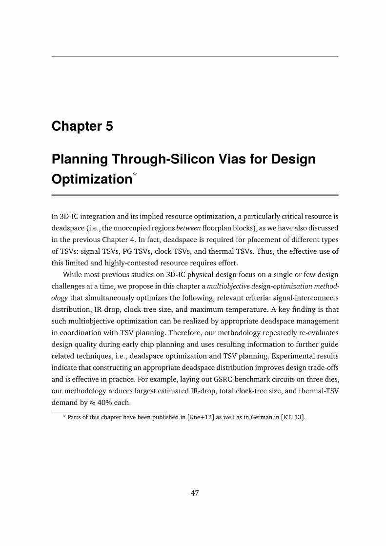
Chapter 5
Planning Through-Silicon Vias for DesignOptimization*
In 3D-IC integration and its implied resource optimization, a particularly critical resource is
deadspace (i.e., the unoccupied regions between floorplan blocks), as we have also discussed
in the previous Chapter 4. In fact, deadspace is required for placement of different types
of TSVs: signal TSVs, PG TSVs, clock TSVs, and thermal TSVs. Thus, the effective use of
this limited and highly-contested resource requires effort.
While most previous studies on 3D-IC physical design focus on a single or few design
challenges at a time, we propose in this chapter a multiobjective design-optimization method-
ology that simultaneously optimizes the following, relevant criteria: signal-interconnects
distribution, IR-drop, clock-tree size, and maximum temperature. A key finding is that
such multiobjective optimization can be realized by appropriate deadspace management
in coordination with TSV planning. Therefore, our methodology repeatedly re-evaluates
design quality during early chip planning and uses resulting information to further guide
related techniques, i.e., deadspace optimization and TSV planning. Experimental results
indicate that constructing an appropriate deadspace distribution improves design trade-offs
and is effective in practice. For example, laying out GSRC-benchmark circuits on three dies,
our methodology reduces largest estimated IR-drop, total clock-tree size, and thermal-TSV
demand by ≈ 40% each.
* Parts of this chapter have been published in [Kne+12] as well as in German in [KTL13].
47

Chapter 5. Planning Through-Silicon Vias for Design Optimization
5.1 Deadspace Requirements for Optimized Planning of
Through-Silicon Vias
Early physical-design phases of 3D-IC integration are driven by floorplanning and intercon-
nect planning / TSV placement. These stages are also responsible for regulating the amount
and distribution of deadspace. An important fact is that the same amount of deadspace
can be distributed throughout a die in many different ways. Depending on floorplanning
objectives, blocks—and thus deadspace—are typically distributed to reduce wirelength
and facilitate thermal management [CWZ04; Li+06b; LMH09; Zho+07]. However, other
design concerns like interconnect planning can require blocks to be redistributed (later on).
Such floorplan modifications can be implemented using the notion of spatial slacks [AM03],as we proposed in Chapter 4. Redistributing blocks and deadspace is essential for placing
different types of TSVs and related optimization goals, as we will show in this chapter.
Table 5.1 contrasts properties of different TSV types and outlines resulting requirements
for deadspace distribution. For example, PG TSVs are preferably aligned among adjacent
dies to limit electromigration, IR-drop and routing congestion [Che+11; HL10; HL11;
JL10]. Irregular placement is preferred for all types of TSVs and requires several non-
uniformly distributed regions of deadspace. Given such a spread-out TSV placement,
routing congestions may be limited due to locally low and/or medium TSV densities.
This is emphasized by block-level integration, where only a limited number of global nets
require signal TSVs [SK00].Depending on the die-stacking technique, TSVs may require aligned deadspace regions
on adjacent dies—we refer to this as the deadspace-alignment problem. For B2B die stacking,
this applies to each TSV since they are passing through adjacent substrate layers. For F2B
stacking, alignment should be considered according to Table 5.1. Some studies (Table 5.1)
propose aligned TSV stacks which span multiple dies. Such stacks must be carefully co-
ordinated. First, this requires deadspace alignment. Second, these stacks obstruct many
enclosed routing tracks; connecting the TSVs’ landing pads requires several vias (passing
through all metal layers) to enable proper signal, clock, or power delivery. Besides, we
note that some 3D-IC designs contain NoCs, i.e., massive interconnect structures [Loi+11;
MWH12; Pas09]. They can be realized by groups of TSVs placed within or closely nearby
the related macro blocks (Chapter 6). This may require aligned deadspace as well.
48

Chapter 5. Planning Through-Silicon Vias for Design Optimization
Tabl
e5.
1:Pr
oper
ties
ofdi
ffer
ent
type
sof
TSV
san
dre
late
dde
adsp
ace-
dist
ribu
tion
requ
irem
ents
.
Type
Dia
met
erA
lignm
ent
Loca
lDen
sity
Pref
erre
dPl
acem
ent
Dea
dspa
ceR
equi
rem
ents
nonu
nifo
rm;
Sign
al≈
2–20µ
mso
met
imes
enco
urag
edlo
w–h
igh
irre
gula
r;po
ssib
lygr
oupe
dsm
all–
larg
eco
ntig
uous
regi
ons;
[HC
H13
;Li+
06a]
[HB
C13
;HL1
2;K
TL12
;TW
H11]
poss
ibly
alig
ned
nonu
nifo
rm;
Ther
mal≈
2–40µ
men
cour
aged
low
–med
ium
irre
gula
rsm
all–
med
ium
cont
igou
sre
gion
s;
[Bud+
13;C
he+
11;H
CH
13]
[CLS
11;C
WZ0
4;Li+
06b]
poss
ibly
alig
ned
nonu
nifo
rm;
Pow
er/≈
10–4
0µ
mst
rong
lypr
efer
red
low
irre
gula
rsm
allc
onti
gous
regi
ons;
Gro
und
[Che+
11;H
L10;
HL1
1;JL
10]
[Fal+
10;H
L10;
HL1
1;JL
10]
nece
ssar
ilyal
igne
d
nonu
nifo
rm;
Clo
ck≈
2–20µ
mso
met
imes
enco
urag
edlo
wir
regu
lar
smal
lcon
tigo
usre
gion
s;
[ZL1
0][Z
L10;
ZML1
1]po
ssib
lyal
igne
d
49
Chapter 5. Planning Through-Silicon Vias for Design Optimization
5.2 Multiobjective Design Optimization of 3D Integrated
Circuits
While previous work succeeds in addressing individual challenges for 3D-IC integration, a
unified approach—to simultaneously address major requirements and provide efficient
design-quality analysis—remains a key challenge. The closest prior work is presented by
Lee and Lim [LL11]. However, they consider only gate-level integration and ignore clock
networks. Also, their deadspace optimization is restricted to thermal TSVs.
In the previous section, we outlined how prior work in (block-level) 3D-IC integration
has been relying on specific deadspace-distribution characteristics. In case these require-
ments are not satisfied, we (Chapter 4) and others [CWZ04; He+09; Li+06a; Li+08]propose to redistribute deadspace. However, prior work mainly focuses on single-objective
deadspace optimization, which may undermine overall design quality. In contrast, multiob-
jective optimization offers a greater promise, as confirmed by our experiments (Section 5.3).
Such optimization requires understanding of the impact of different TSV-planning phases
on design quality, as well as techniques for multiobjective deadspace optimization. Note
that multiobjective deadspace optimization seeks to improve block and TSV placement in
order to diminish TSV overhead and account for multiple design constraints and optimiza-
tion goals. Such an optimization process can be successfully implemented during early
design phases, as described in this chapter.
5.2.1 Methodology Overview and Configuration
In order to enable multiobjective design optimization, we propose a methodology which
can guide existing 3D-IC design flows and provide feedback to specific design steps. We
construct a design-flow extension using our algorithms and available 3D design tools. The
approach is modular and can be extended to accommodate other tools or stages.
Our proposed design-flow extension called MoDo is illustrated in Figure 5.1; it is based
on an incremental process aiming for deadspace-optimized floorplans which satisfy multiple
design criteria. As is typical in modular 3D-IC design flows, TSV planning can be separated
from the floorplanning and/or placement stages. Thus, the main loop encapsulating TSV
planning and deadspace optimization seeks to (i) determine appropriate TSV sites, likely
requiring deadspace redistribution and/or alignment, (ii) place a TSV into or near the
site, and (iii) perform deadspace optimization considering updated TSV sites. To guide
50
Chapter 5. Planning Through-Silicon Vias for Design Optimization
TSV planning, related quality-analysis metrics are evaluated during iterations. After the
main loop has converged, overall design quality is evaluated, possibly restarting global
optimization (global loop). Our algorithms and methodology are presented next; additional
implementation details and parameter values are provided in Subsection 5.3.1.
We assume a notation similar to the problem formulation given in Section 4.2.1.
Given a 3D-IC design, we perform the following methodology-configuration steps.
First, an initial 3D floorplan is obtained (Subsection 5.3.1). This floorplan provides the
inter-die block partitioning and preliminary block locations. Second, a die ordering to
improve the thermal distribution and to minimize the TSV count is performed. Given
|D| dies, we analyse all |D|! possible die sequences. For each sequence, we estimate the
power distribution and the signal-TSV count. The sequence with the lowest cost Γseq =wseq∗γP,norm+
1−wseq
∗γTSV,norm is chosen where γP,norm and γTSV,norm denote normalized
and weighted power distribution and TSV count, respectively. Note that die ordering is
performed only once initially, i.e., not during subsequent global-loop iterations. Third, the
total TSV count is estimated. In addition to the fixed signal-TSV count, a conservative
estimate for PG, clock, and thermal TSVs is taken into account (Subsection 5.2.4). Fourth,
the required deadspace amount is determined and annotated for each die. This accounts
for TSV footprints and possibly for some design-specific deadspace requirements.
5.2.2 Techniques for Deadspace Optimization
Note that the main loop including TSV planning (Subsection 5.2.4) and deadspace optimiza-
tion is a key part of MoDo. Thereby, TSV planning seeks to guide deadspace optimization
and thus to address the following concerns.
• Managing deadspace utilization, i.e., regulate the TSV count and determine TSV
sites. Given that TSVs of different types compete for available deadspace, managing
the utilization directly impacts design quality.
• Accounting for deadspace-distribution requirements (Section 5.1) eases TSV
placement. Once TSV sites are determined, they are considered as rectangular blocks,
occupying some amount of deadspace. This resource accounting is convenient during
subsequent deadspace optimization.
51
Chapter 5. Planning Through-Silicon Vias for Design Optimization
Floorplanning
Design-qualityanalysis
Optimized3D-IC design
3D-ICdesign flow
Methodologyconfiguration
Criteriasatisfied ?Yes No
Deadspaceoptimization
- Die ordering- Control deadspace demand Provide initial floorplan
- Regulate TSV count- Determine TSV sites- Perform deadspaceredistribution & alignment- Shift blocks & TSVs Optimize floorplan
- Determine qual. IR-drop- Determine clock-tree size- Determine signal wirelength- Det. thermal-TSV demand Evaluate overall quality
Globalloop
TSV planning
Placementetc.
3D-IC design
Main loop
Figure 5.1: Main parts of MoDo, integrated in a 3D-IC design flow at early design phases.
52

Chapter 5. Planning Through-Silicon Vias for Design Optimization
• Tackling the deadspace-alignment problem, i.e., aligning deadspace regions to
enable placement of aligned TSVs. To ease placement of all TSVs, those to be aligned
should be considered first.
Addressing these challenges allows us to improve TSV and block placement while
exploiting given deadspace. For that purpose, we invoke deadspace redistribution and
alignment as well as shifting of blocks and TSVs. We limit deadspace insertion because
it can increase area and wirelength overhead (Subsection 4.3.3). However, when design
quality is judged unacceptable, the amount of deadspace must increase to ease deadspace
optimization and TSV insertion. By doing so, we aim to reach the desired design quality
during global-loop iteration(s).
We consider planned TSV sites as movable blocks. This allows us to place TSVs into
nearby deadspace in cases where sites overlap with design blocks. Furthermore, we allow
design blocks to be shifted as well; this enables deadspace redistribution and alignment.1
Thus, strict TSV-placement requirements can also be satisfied. Note that we have to perform
shifting of both blocks and TSVs such that (i) a valid placement can be assured and (ii) the
desired design quality is only marginally affected.
To address both issues, we base our shifting algorithm on the concepts of the constraint
graph (CG) [Kah+11, Chapter 3], range constraints [YCH04] and spatial slacks [AM03].Recall that the concept of spatial slacks is also applied in Chapter 4. Representing a
floorplan using a CG pair (one horizontal and one vertical graph) allows us to maintain
a valid placement and to handle the relations between blocks efficiently. Spatial slacks
describe maximal shifting ranges of blocks within a given floorplan outline, whereas range
constraints are used to limit block shifting—and its impact on design quality w.r.t. altered
layouts—within certain regions.
In our incremental flow, we initially generate the CG pair for each die separately,
considering placed blocks, and update them during TSV planning.2 We transform block and
TSV coordinates (x , y) into range constraints [x−δ, x+δ], [y−δ, y+δ], defining different
shifting windows (Figure 5.2(a)). In order to judge the feasibility of considered sites during
TSV planning, i.e., to evaluate the capabilities for required block shifting, we determine
1These deadspace-optimization techniques may also be implemented in a more explicit manner. However,given that local TSV densities are mostly low or medium (Table 5.1), it appears more appropriate to shiftblocks and/or TSVs in cases of locally lacking deadspace.
2Updating the CGs is trivial if a planned TSV site occurs within deadspace. For cases where the TSV siteoverlaps one or several existing blocks, the respective slacks have to considered. To furthermore minimizerequired shifting, TSV insertion takes place next to the nearest border of the overlapped blocks.
53
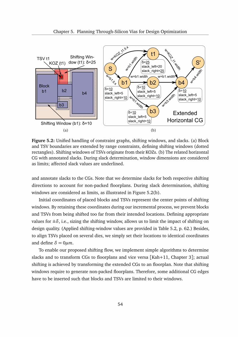
Chapter 5. Planning Through-Silicon Vias for Design Optimization
TSV t1KOZ (t1)
Shifting Win-dow (t1): δ=25
Shifting Window (b1): δ=10
b2
b3
b4
Blockb1
(a)
δ=25slack_left=20slack_right=25
δ=10slack_left=5slack_right=10
δ=10slack_left=5slack_right=10
δ=10slack_left=5slack_right=10
δ=10slack_left=5slack_right=10
SS'
b1 b2 b4
b3
t1
w=b1.ll.x
w=b
1.w
idth
w=b1.width
w=b1.width
w=b1.width
w=b3.w
idth
w=KO
Z_t1.width
w=b
4.w
idth
w=KOZ_t1.ll.x
ExtendedHorizontal CG
(b)
Figure 5.2: Unified handling of constraint graphs, shifting windows, and slacks. (a) Blockand TSV boundaries are extended by range constraints, defining shifting windows (dottedrectangles). Shifting windows of TSVs originate from their KOZs. (b) The related horizontalCG with annotated slacks. During slack determination, window dimensions are consideredas limits; affected slack values are underlined.
and annotate slacks to the CGs. Note that we determine slacks for both respective shifting
directions to account for non-packed floorplans. During slack determination, shifting
windows are considered as limits, as illustrated in Figure 5.2(b).
Initial coordinates of placed blocks and TSVs represent the center points of shifting
windows. By retaining these coordinates during our incremental process, we prevent blocks
and TSVs from being shifted too far from their intended locations. Defining appropriate
values for ±δ, i.e., sizing the shifting window, allows us to limit the impact of shifting on
design quality. (Applied shifting-window values are provided in Table 5.2, p. 62.) Besides,
to align TSVs placed on several dies, we simply set their locations to identical coordinates
and define δ = 0µm.
To enable our proposed shifting flow, we implement simple algorithms to determine
slacks and to transform CGs to floorplans and vice versa [Kah+11, Chapter 3]; actual
shifting is achieved by transforming the extended CGs to an floorplan. Note that shifting
windows require to generate non-packed floorplans. Therefore, some additional CG edges
have to be inserted such that blocks and TSVs are limited to their windows.
54

Chapter 5. Planning Through-Silicon Vias for Design Optimization
5.2.3 Design-Quality Analysis
Our methodology provisions for frequent estimation of design quality; the quality metrics—
referred to as cost terms in the following—are iteratively determined during the main
loop. Thus, we estimate design quality during TSV planning and deadspace optimization
to guide this both alternating and incremental process appropriately. However, we also
seek to evaluate the overall design quality after finishing the main loop and possibly start
over with optimization if costs are not sufficiently reduced. For example, in cases where
our flow fails to reduce cost Γ 0γIR
to Γ optγIR= wopt
γIR∗ Γ 0γIR
, design quality in terms of IR-drop is
not ensured. Thus, additional PG-TSV sites are required; the floorplanner is reconfigured
to increase deadspace, and the main loop is revisited.
5.2.4 Planning Different Types of Through-Silicon Vias
We order TSV types as follows to facilitate deadspace optimization: (i) PG TSVs, (ii) clock
TSVs, (iii) signal TSVs, and (iv) thermal TSVs. The rationale for this ordering is as follows.
First, PG TSVs should be aligned throughout the whole 3D IC and are thus given priority.
Clock TSVs may also be aligned, but not necessarily for the whole stack. Second, critical
PG and clock networks should be planned early. Third, signal-TSV planning adheres some
flexibility for site determination; previously placed TSVs are not expected to significantly
obstruct it. Fourth, all placed TSVs serve also as thermal TSVs and thus facilitate thermal
management. Nevertheless, additional thermal TSVs may be warranted.
For each TSV-planning phase, our algorithms aim for the initial value Γ 0γ
of the corre-
sponding cost γ (e.g., maximum IR-drop Γ 0γIR
) to be reduced to Γ optγ= wopt
γ∗Γ 0γ
by step-wise
planning and placement of TSVs. Note that during each planning phase, deadspace op-
timization is performed in order to remain a valid placement and to obtain deadspace
where required for TSV insertion.
For TSV-count estimates required by methodology configuration, deadspace optimiza-
tion is not performed; all TSV sites are considered as feasible, ignoring possible overlaps.
In this context, TSVs are assumed to be placed (i.e., the actual insertion is skipped) such
that cost terms can be reduced as described above.
In the following subsections, we describe our techniques for TSV planning in detail.
55

Chapter 5. Planning Through-Silicon Vias for Design Optimization
Power/Ground-TSV Planning
Placing irregularly distributed TSVs stacks in high-power regions is most useful for limiting
IR-drop and TSV count (Table 5.1 and Section 2.4). We consider PG-grid structures,
illustrated in Figure 5.3(a); structural properties are described in Subsection 5.3.1.
In order to determine PG-TSV sites, i.e., PG-grid nodes, previous work mostly considers
modified nodal analysis of a equivalent resistance circuit. However, scaling such network
analysis to large designs, resulting in possibly millions of network nodes, is difficult. Hence,
we propose a simplified diagnostic—the qualitative IR-drop distribution. Our approach is
based on the following observations, obtained while performing SPICE-based simulations
for the IR-drop on abstracted PG-grid networks. (See Figure 5.3(b); a simulation result
is illustrated in Figure 5.4.) First, we observe that aligned PG TSVs influence IR-drop in
the circumference of that TSV site on all dies. Second, the IR-drop caused by modules is
distributed less evenly than the drop caused by TSVs and grid wires. Third, the total IR-drop
distribution can be interpreted as the superposition of separate distributions originating
from power-consuming modules. Each distribution can be described using an exponential
function while considering nearby power consumption and PG TSVs.
Applying these observations, we determine the qualitative IR-drop distribution as
follows. First, we construct 2D grids, similar structured as the 3D-IC PG grids. Second,
we sum up power consumption of modules which overlap among different dies in the
3D-IC stack, and assign normalized values P(n) to related nodes n in the 2D grids. Third,
given such 2D lumped-power grids, we determine for each node n, where no TSV is yet
assigned, four power-spreading factors (one for each cardinal direction; see Figure 5.5).
Each of the factors (ale f t , ari ght , atop, and abot tom) is calculated as a = − ln (amin)/dmax
where amin represents a minimal IR-drop factor (Table 5.2) to be reached at distance
dmax away from n; dmax is determined by following the respective grid direction until the
nearest TSV / die boundary is reached. Fourth, we determine the superposition of power-
spreading factors on all nodes, representing the qualitative IR-drop IR′. For a particular
node n, we consider itself and other nodes n′ = n in the same quadrant and determine
IR′(n) = sTSV ∗
P(n) +
n′,a P (n′) ∗ exp (−a ∗ dist(n, n′))
where sTSV is a scaling factor
(Table 5.2) applied for nodes with a TSV assigned. Note that only the two relevant factors
a are considered, i.e., the ones pointing towards n.
Employing the diagnostic of qualitative IR-drop distribution, we perform PG-TSV
planning as follows. First, we consider the largest-value node as TSV site and place a
56
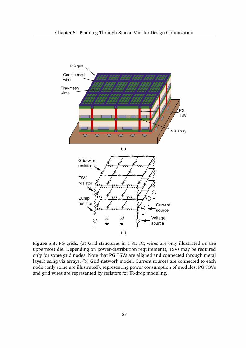
Chapter 5. Planning Through-Silicon Vias for Design Optimization
PG grid
Via array
Coarse-meshwires
Fine-meshwires
PGTSV
(a)
+ − + −
+ −
TSVresistor
Bumpresistor
Grid-wireresistor
Currentsource
Voltagesource
(b)
Figure 5.3: PG grids. (a) Grid structures in a 3D IC; wires are only illustrated on theuppermost die. Depending on power-distribution requirements, TSVs may be requiredonly for some grid nodes. Note that PG TSVs are aligned and connected through metallayers using via arrays. (b) Grid-network model. Current sources are connected to eachnode (only some are illustrated), representing power consumption of modules. PG TSVsand grid wires are represented by resistors for IR-drop modeling.
57
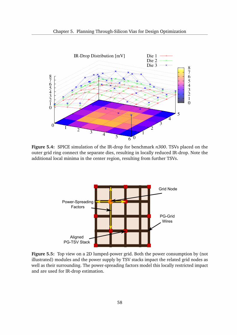
Chapter 5. Planning Through-Silicon Vias for Design Optimization
IR-Drop Distribution [mV] Die 1Die 2Die 3
0 1 2 3 4 5 6 01
23
45
012345678
012345678
Figure 5.4: SPICE simulation of the IR-drop for benchmark n300. TSVs placed on theouter grid ring connect the separate dies, resulting in locally reduced IR-drop. Note theadditional local minima in the center region, resulting from further TSVs.
PG-GridWires
AlignedPG-TSV Stack
Power-SpreadingFactors
Grid Node
Figure 5.5: Top view on a 2D lumped-power grid. Both the power consumption by (notillustrated) modules and the power supply by TSV stacks impact the related grid nodes aswell as their surrounding. The power-spreading factors model this locally restricted impactand are used for IR-drop estimation.
58
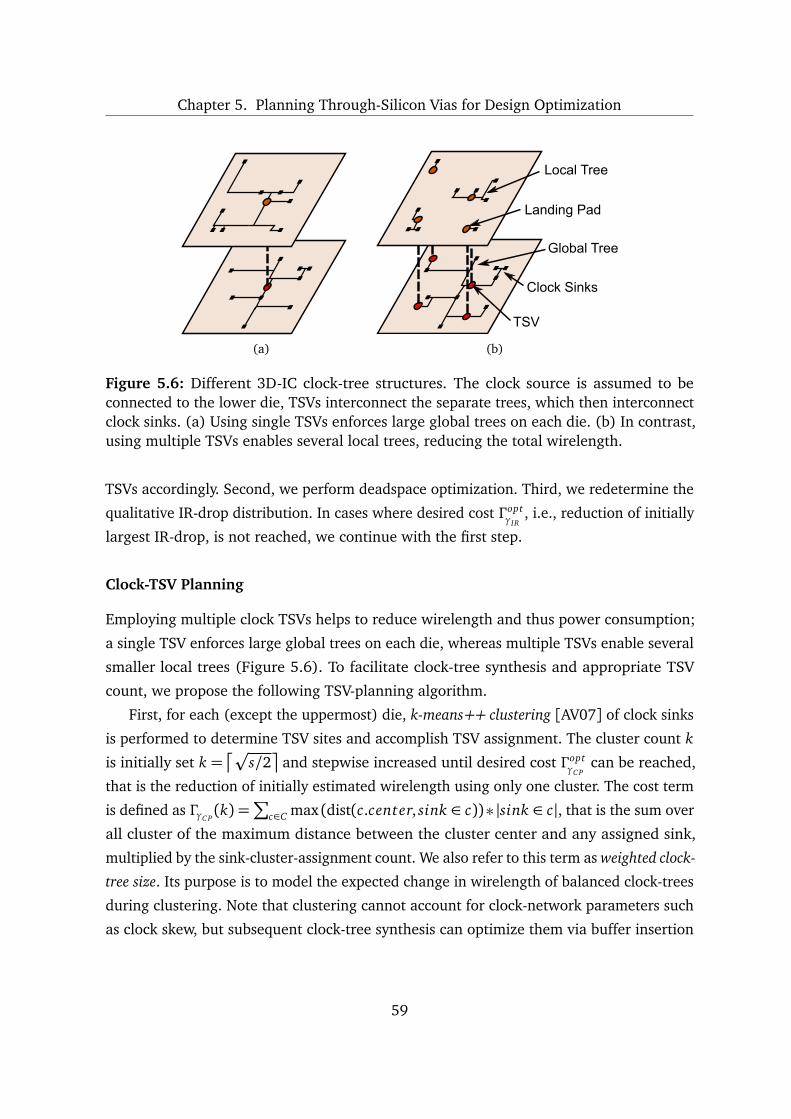
Chapter 5. Planning Through-Silicon Vias for Design Optimization
(a)
TSV
Clock Sinks
Global Tree
Landing Pad
Local Tree
(b)
Figure 5.6: Different 3D-IC clock-tree structures. The clock source is assumed to beconnected to the lower die, TSVs interconnect the separate trees, which then interconnectclock sinks. (a) Using single TSVs enforces large global trees on each die. (b) In contrast,using multiple TSVs enables several local trees, reducing the total wirelength.
TSVs accordingly. Second, we perform deadspace optimization. Third, we redetermine the
qualitative IR-drop distribution. In cases where desired cost Γ optγIR
, i.e., reduction of initially
largest IR-drop, is not reached, we continue with the first step.
Clock-TSV Planning
Employing multiple clock TSVs helps to reduce wirelength and thus power consumption;
a single TSV enforces large global trees on each die, whereas multiple TSVs enable several
smaller local trees (Figure 5.6). To facilitate clock-tree synthesis and appropriate TSV
count, we propose the following TSV-planning algorithm.
First, for each (except the uppermost) die, k-means++ clustering [AV07] of clock sinks
is performed to determine TSV sites and accomplish TSV assignment. The cluster count k
is initially set k =p
s/2
and stepwise increased until desired cost Γ optγC P
can be reached,
that is the reduction of initially estimated wirelength using only one cluster. The cost term
is defined as ΓγC P(k) =
c∈C max (dist(c.center, sink ∈ c))∗ |sink ∈ c|, that is the sum over
all cluster of the maximum distance between the cluster center and any assigned sink,
multiplied by the sink-cluster-assignment count. We also refer to this term as weighted clock-
tree size. Its purpose is to model the expected change in wirelength of balanced clock-trees
during clustering. Note that clustering cannot account for clock-network parameters such
as clock skew, but subsequent clock-tree synthesis can optimize them via buffer insertion
59
Chapter 5. Planning Through-Silicon Vias for Design Optimization
and clock-tree tuning [LM12; ZL12]. If required, clock sinks may be even reassigned to
TSVs or swap assignments with signal TSVs.
Deadspace optimization is then performed after considering determined cluster center
as TSV sites. Thereby, the shifting windows are initially set δC = 0µm to fix the cluster
centers. In case of infeasible TSV insertion, the value is iteratively adapted (Table 5.2).
Signal-TSV Planning
We perform signal-TSV planning similarly as proposed in Section 4.2. However, deadspace
management is differing here as follows. We perform TSV-island insertion, using a local
search, as long as deadspace is locally available. If this fails due to insufficient deadspace,
islands are placed into nearby deadspace whenever possible such that wirelength overheads
as well as efforts for deadspace optimization are limited. The reason for doing so is that
previously placed PG TSVs / clock TSVs are considered as fixed / only marginally shiftable
in order to maintain design quality w.r.t. these critical networks.
Note that we define no cost term for signal-TSV planning since their count is minimized
by die ordering. However, we evaluate the impact of densely packed TSV islands on
wirelength and routing utilization in our experiments, as discussed in Subsection 5.3.2.
Thermal-TSV Planning
Recall that die ordering (Subsection 5.2.1) and aligned TSVs (i.e., mainly PG TSVs) facilitate
thermal management. Nevertheless, we consider the insertion of additional thermal TSVs
to further decrease maximal temperatures.
We leverage findings by Cong et al. [CLS11] for our approach. Initially, we construct 2D
lumped-power grids as proposed for PG-TSV planning. We construct grids for all ordered
subsets d1 , d1, d2 , . . . ,
d1, . . . , d|D|
of dies; d1 denotes the bottom die. The following
steps are then performed independently for each lumped-power grid g and its uppermost
die dtop. First, we determine the TSV count Tcur r(b) for each bin b in dtop. Second, we
determine the ratio r =
b (Tcur r(b)/l p(b)) of dtop ’s total TSV count and g ’s total lumped
power. Third, we determine the desired TSV count Tdes(b) = ⌊0.5+ r ∗ l p(b)⌋ for each b
in dtop. Fourth, we plan sites for b using a local search if Tcur r(b)< Tdes(b); the search is
designed similarly as for signal-TSV planning. Since the last step of TSV placement likely
impacts r, we repeat all enumerated steps until cost Γ optγT
can be reached or no further TSV
60
Chapter 5. Planning Through-Silicon Vias for Design Optimization
can be inserted for any b due to Tcur r(b) = Tdes(b) or lacking deadspace. The initial cost is
defined as Γ 0γT=
b Tdes(b)− Tcur r(b).Note that our approach aims, in practice, for thermal-TSV insertion especially on the
top die of the stack which is adjacent to the heatsink. This die is typically characterized
by largest power-consumption values and likely provides many and/or large deadspace
regions since no/few TSVs are placed yet. Placing thermal TSVs, i.e., increasing the vertical
thermal conductivity directly towards the heatsink, appears thus beneficial.
5.3 Experimental Investigation
In this section, we first discuss the configuration of our methodology, benchmarks, and ex-
periments. Then, we discuss results and our findings on multiobjective design optimizations
by means of interacting TSV planning and deadspace optimization.
5.3.1 Configuration
Methodology Configuration
Parameters introduced in Section 5.2 are summarized in Table 5.2 along with their values.
Initial 3D floorplans are obtained using an academic tool [Zho+07] which accounts for
wirelength, area, and thermal distribution. The tool is configured such that all three
objectives are equally weighted.
Signal-Interconnects Evaluation
Although signal interconnects are not used to control global-loop iterations, they are
evaluated and reported as design-quality criterion. We estimate signal wirelength by
extending the HPWL-based metric BB-2D3D-HPWL (Subsection 4.3.1); here, the overall
wirelength estimate also considers TSVs’ lengths. Besides, to estimate the signal-routing
utilization, we construct separate routing grids for each die using tiles with dimensions
according to signal-TSV dimensions. Each (partial) net is assumed to be routed in L-shaped
wires on the related grid(s); wire segments ws are mapped to the tiles r t they cover. The
average utilization is then determined as u=
d
r t |ws(r t)| × |r t|−1
× |d|−1.
61
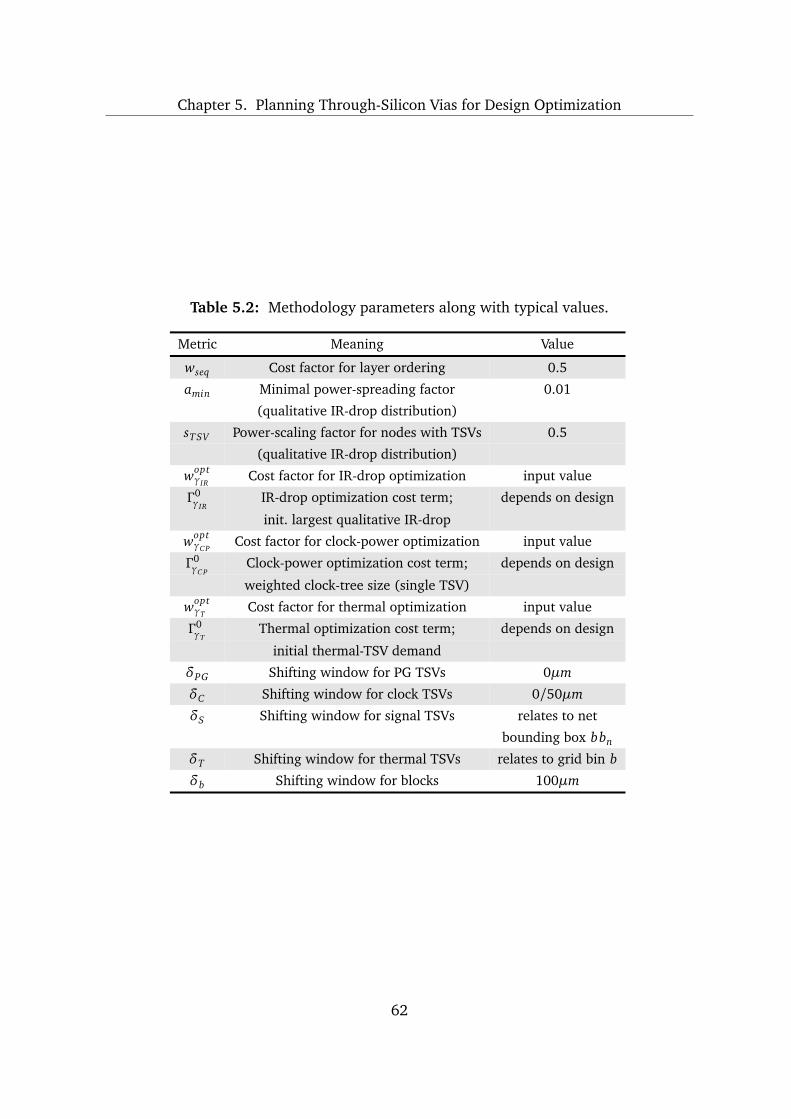
Chapter 5. Planning Through-Silicon Vias for Design Optimization
Table 5.2: Methodology parameters along with typical values.
Metric Meaning Value
wseq Cost factor for layer ordering 0.5
amin Minimal power-spreading factor 0.01
(qualitative IR-drop distribution)
sTSV Power-scaling factor for nodes with TSVs 0.5
(qualitative IR-drop distribution)
woptγIR
Cost factor for IR-drop optimization input value
Γ 0γIR
IR-drop optimization cost term; depends on design
init. largest qualitative IR-drop
woptγC P
Cost factor for clock-power optimization input value
Γ 0γC P
Clock-power optimization cost term; depends on design
weighted clock-tree size (single TSV)
woptγT
Cost factor for thermal optimization input value
Γ 0γT
Thermal optimization cost term; depends on design
initial thermal-TSV demand
δPG Shifting window for PG TSVs 0µm
δC Shifting window for clock TSVs 0/50µm
δS Shifting window for signal TSVs relates to net
bounding box bbn
δT Shifting window for thermal TSVs relates to grid bin b
δb Shifting window for blocks 100µm
62
Chapter 5. Planning Through-Silicon Vias for Design Optimization
3D-IC Configuration and Benchmarks
We consider F2B stacking and via-middle TSVs (Figure 1.4; Section 1.2) with a diameter
of 4µm and a square KOZ with dimensions of 8µm × 8µm. PG-TSVs are larger, with a
diameter of 8µm and a KOZ of 12µm×12µm. Signal and thermal TSVs are grouped as TSV
islands; individual KOZs are, therefore, reduced to 6µm× 6µm. Dies are thinned down to
40µm. Metal layers are 4µm and bonding layers are 2µm thick. Power and ground grids
are offset by 12µm. Note that die boundaries are extended by 24µm to enable PG-TSV
rings. Coarse PG-grid wires are 8µm wide, 0.8µm thick, and their pitch is 80µm; this pitch
also applies to PG TSVs.
Experiments are conducted using representative GSRC benchmarks [GSRC00] with
the following modifications. External pins are represented by package bumps; nets linked
to such pins must thus connect through to the lowermost die. Each block is assumed to
have multiple spread-out clock sinks, one placed at the block’s center and four placed in
the corners. Net pins are placed at the related block’s center.
Experimental Configuration
Our experiments validate the capabilities of our methodology for multiobjective design
optimization. We independently decrease the different cost factors woptγ
in steps of 10%, in
the range from 90% to 40%. Experiments sweep through the parameter space; best results
are reported in Table 5.3. Estimated cost reductions determined by final design-quality
analysis are labeled as “↓”; they typically correlate to 100%−woptγ
.
Results are compared to the following settings, subsequently referred to as baseline
cases. For IR-drop optimization, PG-TSVs are only placed on the rings. For clock-power
optimization, single clusters define global TSV sites on each die. For interconnects opti-
mization, signal TSVs are not densely packed into islands but placed separately. For thermal
optimization, no additional thermal TSVs are considered on any die and no redundant PG
TSVs are placed in the uppermost die.
If the deadspace amount is insufficient to reach the desired cost reductions, our method-
ology requests the floorplanner to increase deadspace. Our experiments swept the range
from 10% to 60% in 10%-steps.3
3We observe that the initial deadspace obtained by [Zho+07] does not scale well with the requestedamount. However, our methodology is able to handle this shortcoming by monitoring the reachable designcost and the additionally required deadspace.
63

Chapter 5. Planning Through-Silicon Vias for Design Optimization
Tabl
e5.
3:R
esul
tsfo
rap
plyi
ngM
oDo
onG
SRC
benc
hmar
ks.
2D
ies
3D
ies
4D
ies
Met
ric
n100
n200
n300
n100
n200
n300
n100
n200
n300
Init
.lar
gest
qual
itat
ive
IR-d
rop
0.26
050.
2492
0.48
220.
2333
0.25
020.
4108
0.23
760.
2196
0.40
37Q
ualit
ativ
eIR
-dro
p↓
(%)
40.2
330
.85
30.2
134
.27
51.6
445
.46
37.9
838
.03
42.3
0IR
-dro
pre
d.de
t.by
SPIC
Esi
m.(
%)
52.4
941
.57
39.8
039
.45
49.4
455
.15
32.5
031
.88
44.1
2In
it.w
eigh
ted
cloc
k-tr
eesi
ze∗
(µm
)13
9231
2654
8047
7488
1038
0223
4309
3777
1192
468.
617
9463
3323
38W
eigh
ted
cloc
k-tr
eesi
ze↓
(%)
31.8
530
.39
30.7
423
.03
42.5
041
.27
29.1
843
.07
37.5
3In
it.t
herm
al-T
SVde
man
d∗30
748
653
956
988
710
3785
016
1717
79Th
erm
al-T
SVde
man
d↓
(%)
21.0
251
.83
61.3
930
.37
77.1
422
.58
23.9
214
.84
16.5
0Es
t.si
gnal
WL
(µm
)13
5588
2984
0040
7762
1466
9034
4503
4592
0316
4400
4421
4759
9411
Est.
sign
al-W
Lre
d.(%
)8.
0616
.71
7.24
11.4
019
.24
n.a.∗∗∗
11.2
9n.
a.∗∗∗
n.a.∗∗∗
Est.
sign
al-r
outi
ngut
il.in
cr.(
%)
-8.3
5-1
7.48
-8.4
1-1
2.60
-20.
77n.
a.∗∗∗
-13.
59n.
a.∗∗∗
n.a.∗∗∗
PG-T
SVco
unt∗
9292
110
108
115
131
128
109
166
Clo
ck-T
SVco
unt∗
68
86
1216
918
12Th
erm
al-T
SVco
unt∗
222
305
307
189
393
186
202
148
142
Sign
al-T
SVco
unt∗
464
935
1123
838
1714
2022
1235
2455
2879
Die
area
µm
2
2065
2820
6540
2626
5612
4906
1660
3618
7740
1127
0010
4940
1542
98In
ital
min
.dea
dspa
ce∗∗
(%)
55.6
556
.97
46.9
551
.61
64.6
050
.61
59.3
257
.36
54.6
9Fi
nalm
in.d
eads
pace∗∗
(%)
33.7
921
.04
15.3
219
.85
16.9
28.
7126
.40
3.14
4.04
∗ Ref
ers
toth
eto
talv
alue
cons
ider
ing
alld
ies.
∗∗R
efer
sto
the
min
imal
valu
eof
alld
ies.
Exte
nded
boun
dary
regi
ons
for
PG-T
SVri
ngs
are
incl
uded
;TSV
KOZs
are
excl
uded
.∗∗∗
Sign
al-T
SVpl
anni
ngw
itho
utco
nsid
erin
gpa
ckin
gw
asin
feas
ible
for
the
give
nou
tlin
e.
64
Chapter 5. Planning Through-Silicon Vias for Design Optimization
5.3.2 Results and Discussion
Experimental results presented in Table 5.3 suggest several observations.
First, our methodology enables a tangible increase of deadspace utilization; in all
experiments, most of deadspace finds good use, with < 5% deadspace left in some cases.
Second, multiple deadspace-distribution requirements can be satisfied during early chip-
planning phases; this enables a multiobjectively optimized design. However, the prospects
for optimization depend on initial floorplans. A large amount of available deadspace may
not be sufficient per se; the relative block ordering and correspondingly available spatial
slacks are also important. For example, consider the benchmark n100. It is characterized
by large slacks due to a small block count. Comparing to results for other benchmarks, we
observe that reachable cost reductions are on average not worse, despite smaller initial
deadspace ratio.
Third, we note that the deadspace-alignment problem can be successfully addressed
within our methodology by sizing shifting windows to δ = 0.
Fourth, the die count impacts design optimization results. The best results are typically
obtained for three-die chips. On the one hand, using four dies—and consequently a larger
amount of total deadspace—may not be justified. Different optimization steps require more
TSVs to maintain quality, thus increasing overhead and cost while decreasing deadspace-
optimization chances. On the other hand, considering two dies typically results in decreased
slacks, thus also limits the options for optimization.
Fifth, the dimensions of shifting windows influence deadspace optimization and thus
TSV planning. For example, we observe that increasing δC above 50µm is counterproductive
in terms of weighted clock-tree size reduction. Furthermore, the initial value of δb = 50µm
resulted in worse cost reductions, mainly for IR-drop reduction.
Based on experimental results, we also made the following general observations on
3D-IC integration of the GSRC benchmarks.
First, the signal-wirelength reduction due to packing TSVs into islands scales with the
amount of interconnect, as expected.4 Interestingly, the average signal-routing utilization
is reduced for the TSV-islands setup; this is possibly due to small spatial offsets for TSVs
4Note that this scenario is different from the experiments conducted in Section 4.3. Here, we neglect toreduce/share KOZs of adjacent TSVs for the baseline case, i.e., while placing single TSVs. In Section 4.3(Table 4.4), such sharing of KOZs was considered for “trivial” TSVs islands containing only one TSV. Theresults described here are thus more pessimistic and reveal larger wirelength estimates for placing singleTSVs than compared to employing TSV islands.
65

Chapter 5. Planning Through-Silicon Vias for Design Optimization
0 1 2 3 4 5 6 01
23
45
00.050.10.150.20.25
00.050.10.150.20.25
Figure 5.7: Qualitative IR-drop distribution on the power grid of benchmark n300, inte-grated on three dies.
embedded in different islands. This way, wires connecting to landing pads of different
islands can be assigned to different routing tracks in most cases. However, the estimated
wirelength increases notably with the die count, which favors integration using only two
dies. This increase is presumably due to longer interconnects passing multiple dies—mainly
caused by nets connecting to external pins—which undermines wirelength reduction by
shorter inter-die routes.5
Second, weighted clock-tree sizes decrease with increasing die count. Smaller sizes
indicate lower power consumption; considering more dies is thus effective for measures of
clock-power optimization.
Third, our proposed IR-drop optimization is effective when using two or three dies but
limited in case of four dies. Also, the initially largest qualitative IR-drop decreases with
die count in some cases. Both observations are possibly due to closer packing of blocks.
Figure 5.7 illustrates the qualitative IR-drop distribution of the benchmark n300 integrated
on three dies; compare to Figure 5.4 for the corresponding SPICE simulation.
5Depending on die thickness, insertion of multiple TSVs per net may reduce wirelength [KTL12]. However,we neglected such scenario; this would notably increase TSV count and thus directly affect cost as well asoverall optimization prospects.
66
Chapter 5. Planning Through-Silicon Vias for Design Optimization
Fourth, the thermal-TSV demand increases with die count, as expected. This is due to
closer packing and stacking of blocks. Similar to IR-drop optimization, considering four
dies is not appropriate w.r.t. thermal optimization.
In summary, these general observations on 3D-IC integration of the GSRC benchmarks
suggest that a limited die count helps to maintain overall design quality.
To validate our qualitative IR-drop distribution, we perform SPICE simulations of
the PG grids with planned PG TSVs. The resistance of PG TSVs is calculated as RTSV ≈16mΩ, considering the electrical resistivity of copper ρCu = 0.02Ωµm and TSV properties
(Subsection 5.3.1). Grid-wire resistances are calculated in a similar way. A voltage source
supplying 1V is assumed to be connected to the lowermost die by placed PG TSVs. SPICE-
simulation results for the IR-drop reduction are given in Table 5.3. We observe that our
qualitative IR-drop distribution tends to underestimate simulated IR-drop reduction by on
average 7.5% for integration using two or three dies, and to overestimate it by on average
3.3% for four-die integration. Thus, our proposed diagnostic is able to measure IR-drop
distributions with acceptable limitations of accuracy.
We validate our thermal-TSV planning algorithm by performing finite element analysis
(FEA) of the 3D-IC stacks. Therefore, we employ the open-source tools SALOME [SAL]and Elmer [ELM], where SALOME generates finite-element meshes to facilitate heat-
transfer modeling in Elmer. Considered dimensions result from the 3D-IC configuration
(Subsection 5.3.1). For thermal conductivity λ
Wm×K
, the following values are assumed:
for dies (silicon) λSi = 130, for TSVs (copper) λCu = 395, and for the bonding layer and
metal layers λBEOL = 66. The heatsink atop has a heat transfer coefficient h = 0.1 Wm2×K
and an ambient temperature T = 300K. Performing FEA after deadspace optimization,
we observe that maximal-temperatures reduction does not scale well with the number
of placed thermal TSVs—temperature reductions are mainly below 4% while comparing
optimized layouts to baseline layouts. However, considering the initially optimized thermal
distribution (Subsection 5.2.1) and the increase of vertical thermal conductivity due to
previously TSVs, this reduction appears reasonable. Furthermore, we note that the cost for
additional thermal TSVs is limited; the ratio of thermal TSVs to all TSVs is below 17% on
average. Figure 5.8 illustrates a FEA-derived temperature plot for the benchmark n100.
For illustration purposes of the final block and TSV arrangement, Figure 5.9 provides
the floorplan of benchmark n300 integrated on three dies.
67
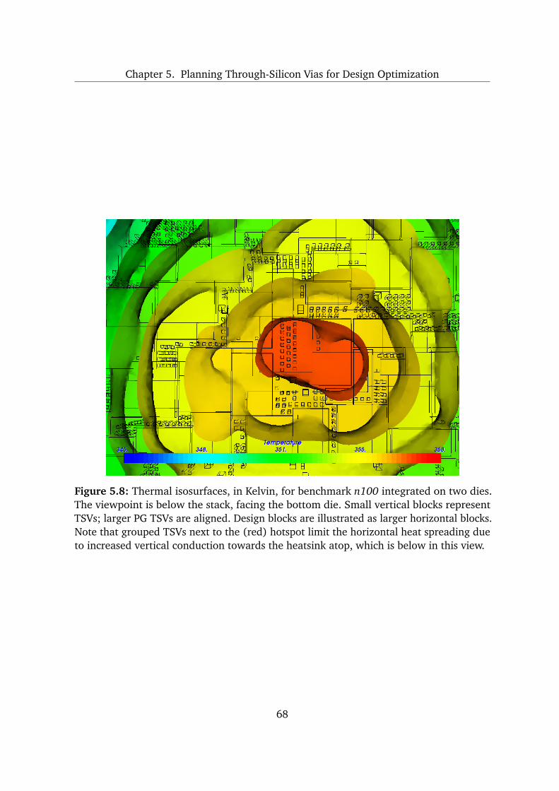
Chapter 5. Planning Through-Silicon Vias for Design Optimization
Figure 5.8: Thermal isosurfaces, in Kelvin, for benchmark n100 integrated on two dies.The viewpoint is below the stack, facing the bottom die. Small vertical blocks representTSVs; larger PG TSVs are aligned. Design blocks are illustrated as larger horizontal blocks.Note that grouped TSVs next to the (red) hotspot limit the horizontal heat spreading dueto increased vertical conduction towards the heatsink atop, which is below in this view.
68
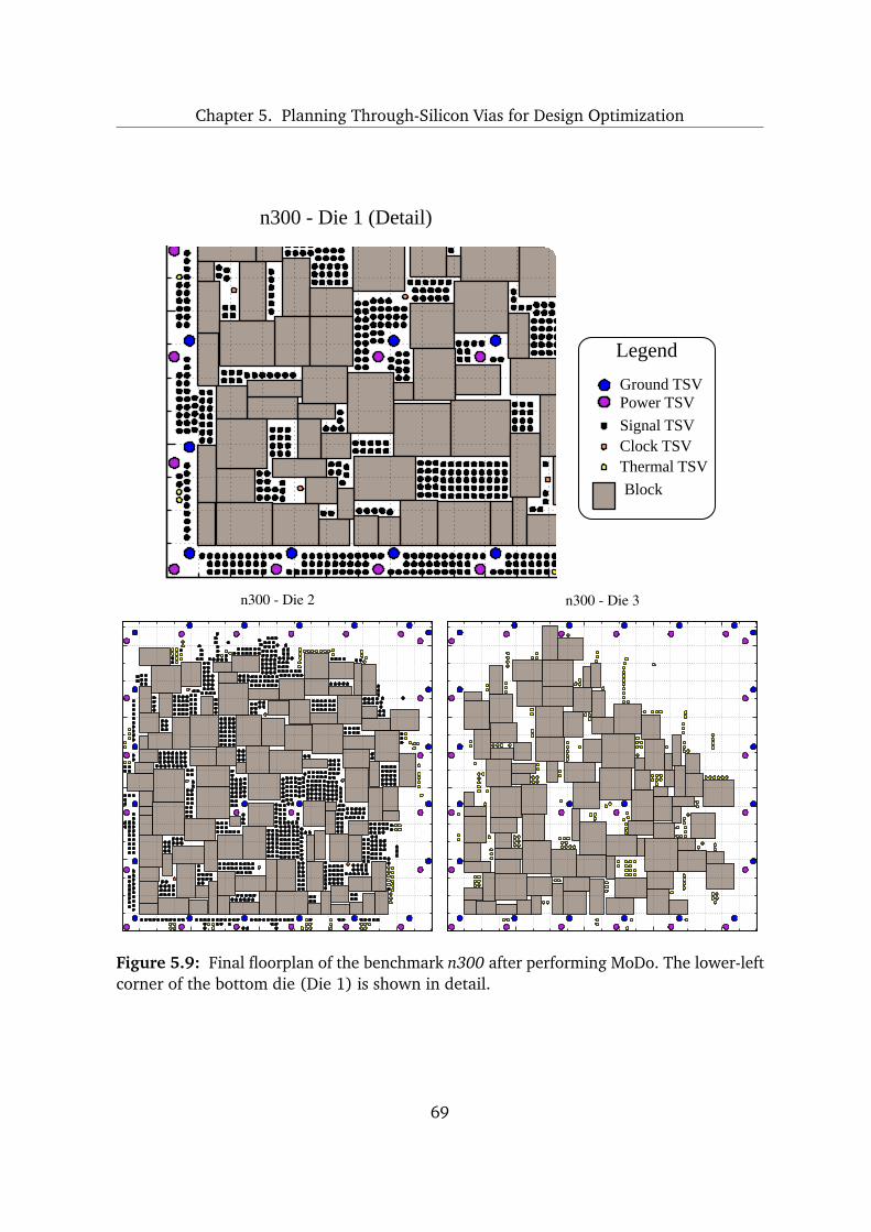
Chapter 5. Planning Through-Silicon Vias for Design Optimization
n300 - Die 1 (Detail)
Legend
Ground TSVPower TSV
Signal TSVClock TSVThermal TSV
Block
n300 - Die 2 n300 - Die 3
Figure 5.9: Final floorplan of the benchmark n300 after performing MoDo. The lower-leftcorner of the bottom die (Die 1) is shown in detail.
69
Chapter 5. Planning Through-Silicon Vias for Design Optimization
5.4 Summary and Conclusions
In this chapter, we proposed multiobjective design optimization for 3D ICs. A key concept of
our approach is to focus on deadspace, a critical resource for 3D-IC integration. Deadspace
is limited and highly contested because it is required for several design tasks during early
chip planning, most importantly for planning different types of TSVs. To facilitate these
tasks, we present a lightweight and modular optimization methodology.
We initially identify deadspace-distribution requirements for key design challenge of
3D ICs. We observe that these different requirements should be simultaneously satisfied in
order to effectively improve design quality. To do so, we develop a design-flow extension
which incorporates algorithmic optimization for TSV planning, deadspace optimization, as
well as design-quality evaluation.
Experimental results show that our methodology can simultaneously optimize in-
terconnect structures, maximum temperature, estimated IR-drop and clock-tree size by
improving deadspace distributions. This is achieved by guided interaction of TSV planning
and deadspace management. As for TSV planning, we successfully evaluate our tech-
niques by experimental comparison to dedicated baseline cases. Additionally, our proposed
techniques for estimating IR-drop and thermal-TSV planning are analysed in more detail.
Regarding the prospects of block-level 3D-IC design, we note that a greater die count
leads to greater TSV overhead and may thus undermine overall design quality. This suggests
to limit the die count and, more importantly, indicates the need for careful design-space
exploration w.r.t. stacking configurations for 3D ICs.
70
Chapter 6
3D Floorplanning for Structural Planning ofMassive Interconnects*
High-performance and/or highly-parallel 3D ICs—as successfully demonstrated in [Bor11;
Fic+13; Jun+13; Kim+12; TLF12]—rely on optimized massive interconnect structures;
hundreds or even thousands of routes are linking blocks which are spread among one
or multiple dies. In this context, 3D NoC architectures have been proposed to increase
communication capabilities for logic integration [Loi+11; MWH12] and for many-core
devices with dedicated memory architectures [Li+06a; Sew12]. Complementing such
approaches, the well-known concept of bus planning, i.e., grouping multiple signals into
adjacent wires, remains also relevant for 3D-IC design.
In this chapter, we demonstrate how both 2D and 3D block alignment can be effectively
utilized for structural planning of different massive interconnect structures. We implement
block alignment for improved efficiency during early design phases, namely during floor-
planning. Besides block alignment, our simulated annealing (SA)-based floorplanning tool
accounts for key objectives in 3D-IC design like fast thermal management, fixed-outline
floorplanning, and layout compaction. Experimental results on GSRC and IBM-HB+ circuits
demonstrate the capabilities of our tool for both planning massive 3D-IC interconnects
and for 3D floorplanning in general.
* Parts of this chapter have been published in [KYL14].
71
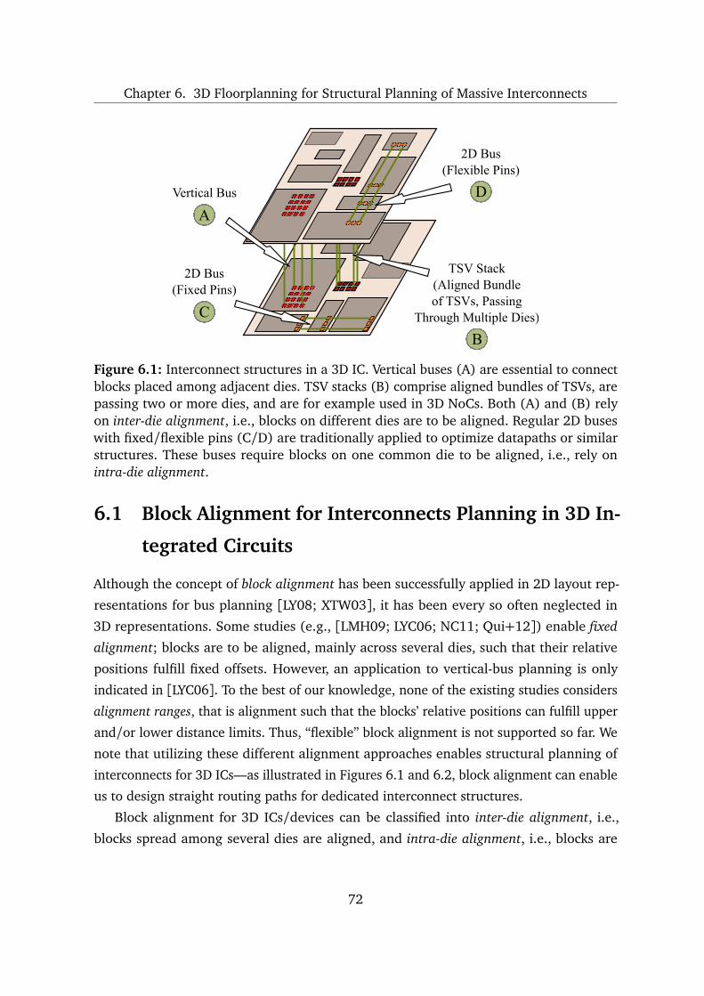
Chapter 6. 3D Floorplanning for Structural Planning of Massive Interconnects
B
TSV Stack(Aligned Bundleof TSVs, Passing
Through Multiple Dies)
A
Vertical Bus D
2D Bus(Flexible Pins)
C
2D Bus(Fixed Pins)
Figure 6.1: Interconnect structures in a 3D IC. Vertical buses (A) are essential to connectblocks placed among adjacent dies. TSV stacks (B) comprise aligned bundles of TSVs, arepassing two or more dies, and are for example used in 3D NoCs. Both (A) and (B) relyon inter-die alignment, i.e., blocks on different dies are to be aligned. Regular 2D buseswith fixed/flexible pins (C/D) are traditionally applied to optimize datapaths or similarstructures. These buses require blocks on one common die to be aligned, i.e., rely onintra-die alignment.
6.1 Block Alignment for Interconnects Planning in 3D In-
tegrated Circuits
Although the concept of block alignment has been successfully applied in 2D layout rep-
resentations for bus planning [LY08; XTW03], it has been every so often neglected in
3D representations. Some studies (e.g., [LMH09; LYC06; NC11; Qui+12]) enable fixed
alignment; blocks are to be aligned, mainly across several dies, such that their relative
positions fulfill fixed offsets. However, an application to vertical-bus planning is only
indicated in [LYC06]. To the best of our knowledge, none of the existing studies considers
alignment ranges, that is alignment such that the blocks’ relative positions can fulfill upper
and/or lower distance limits. Thus, “flexible” block alignment is not supported so far. We
note that utilizing these different alignment approaches enables structural planning of
interconnects for 3D ICs—as illustrated in Figures 6.1 and 6.2, block alignment can enable
us to design straight routing paths for dedicated interconnect structures.
Block alignment for 3D ICs/devices can be classified into inter-die alignment, i.e.,
blocks spread among several dies are aligned, and intra-die alignment, i.e., blocks are
72
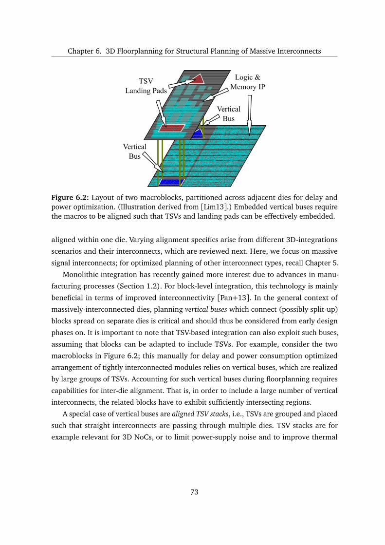
Chapter 6. 3D Floorplanning for Structural Planning of Massive Interconnects
TSVLanding Pads
Logic &Memory IP
VerticalBus
VerticalBus
Figure 6.2: Layout of two macroblocks, partitioned across adjacent dies for delay andpower optimization. (Illustration derived from [Lim13].) Embedded vertical buses requirethe macros to be aligned such that TSVs and landing pads can be effectively embedded.
aligned within one die. Varying alignment specifics arise from different 3D-integrations
scenarios and their interconnects, which are reviewed next. Here, we focus on massive
signal interconnects; for optimized planning of other interconnect types, recall Chapter 5.
Monolithic integration has recently gained more interest due to advances in manu-
facturing processes (Section 1.2). For block-level integration, this technology is mainly
beneficial in terms of improved interconnectivity [Pan+13]. In the general context of
massively-interconnected dies, planning vertical buses which connect (possibly split-up)
blocks spread on separate dies is critical and should thus be considered from early design
phases on. It is important to note that TSV-based integration can also exploit such buses,
assuming that blocks can be adapted to include TSVs. For example, consider the two
macroblocks in Figure 6.2; this manually for delay and power consumption optimized
arrangement of tightly interconnected modules relies on vertical buses, which are realized
by large groups of TSVs. Accounting for such vertical buses during floorplanning requires
capabilities for inter-die alignment. That is, in order to include a large number of vertical
interconnects, the related blocks have to exhibit sufficiently intersecting regions.
A special case of vertical buses are aligned TSV stacks, i.e., TSVs are grouped and placed
such that straight interconnects are passing through multiple dies. TSV stacks are for
example relevant for 3D NoCs, or to limit power-supply noise and to improve thermal
73
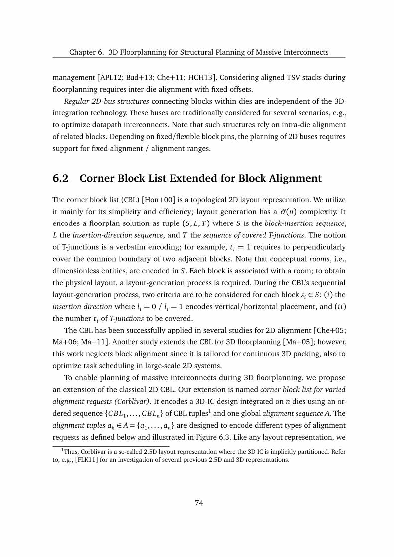
Chapter 6. 3D Floorplanning for Structural Planning of Massive Interconnects
management [APL12; Bud+13; Che+11; HCH13]. Considering aligned TSV stacks during
floorplanning requires inter-die alignment with fixed offsets.
Regular 2D-bus structures connecting blocks within dies are independent of the 3D-
integration technology. These buses are traditionally considered for several scenarios, e.g.,
to optimize datapath interconnects. Note that such structures rely on intra-die alignment
of related blocks. Depending on fixed/flexible block pins, the planning of 2D buses requires
support for fixed alignment / alignment ranges.
6.2 Corner Block List Extended for Block Alignment
The corner block list (CBL) [Hon+00] is a topological 2D layout representation. We utilize
it mainly for its simplicity and efficiency; layout generation has a O (n) complexity. It
encodes a floorplan solution as tuple (S, L, T) where S is the block-insertion sequence,
L the insertion-direction sequence, and T the sequence of covered T-junctions. The notion
of T-junctions is a verbatim encoding; for example, t i = 1 requires to perpendicularly
cover the common boundary of two adjacent blocks. Note that conceptual rooms, i.e.,
dimensionless entities, are encoded in S. Each block is associated with a room; to obtain
the physical layout, a layout-generation process is required. During the CBL’s sequential
layout-generation process, two criteria are to be considered for each block si ∈ S: (i) the
insertion direction where li = 0 / li = 1 encodes vertical/horizontal placement, and (ii)the number t i of T-junctions to be covered.
The CBL has been successfully applied in several studies for 2D alignment [Che+05;
Ma+06; Ma+11]. Another study extends the CBL for 3D floorplanning [Ma+05]; however,
this work neglects block alignment since it is tailored for continuous 3D packing, also to
optimize task scheduling in large-scale 2D systems.
To enable planning of massive interconnects during 3D floorplanning, we propose
an extension of the classical 2D CBL. Our extension is named corner block list for varied
alignment requests (Corblivar). It encodes a 3D-IC design integrated on n dies using an or-
dered sequence CBL1, . . . , CBLn of CBL tuples1 and one global alignment sequence A. The
alignment tuples ak ∈ A= a1, . . . , an are designed to encode different types of alignment
requests as defined below and illustrated in Figure 6.3. Like any layout representation, we
1Thus, Corblivar is a so-called 2.5D layout representation where the 3D IC is implicitly partitioned. Referto, e.g., [FLK11] for an investigation of several previous 2.5D and 3D representations.
74

Chapter 6. 3D Floorplanning for Structural Planning of Massive Interconnects
s1
s2
s3
s4
s5
s6
s7
s8
s9
s10s11
200 units
400
units
(A) a1 = (s1, s2, (40, 1), (40, 1))
(C) a3 = (s9, s10, (150, 2), (0, 0)), a4 = (s9, s11, (150, 2), (0, 0))
Alignment Encoding
(B) a2 = (s7, s8, (0, 0), (0,0))
(D) a5 = (s3, s4, (30, 1), (150, 2)), a6 = (s4, s5, (30, 1), (150, 2)), a7 = (s5, s6, (30, 1), (150, 2))
B
TSV Stack(Aligned Bundleof TSVs, Passing
Through Multiple Dies)
A
Vertical Bus D
2D Bus(Flexible Pins)
C
2D Bus(Fixed Pins)
Figure 6.3: Interconnect structures in a 3D IC and related block-alignment encoding.
have to embed Corblivar in a floorplanning tool; core parts and main features of our tool
are outlined in Figure 6.4.
6.2.1 Alignment Encoding
Definition of Alignment Tuples
Assume the placement of block s j has to consider some alignment w.r.t. block si. The related
request is then defined as tuple ak =
si, s j, (ARx , ARTx), (AR y , ARTy)
where (ARx , ARTx)and
AR y , ARTy
denote the partial requests w.r.t. the x- and y-coordinate. These requests
can be independently defined as fixed offsets (ART = 0), as minimal overlaps (ART = 1), as
maximal distances (ART = 2), or as don’t cares (ART = −1); the meaning of these types is
explained next.
75
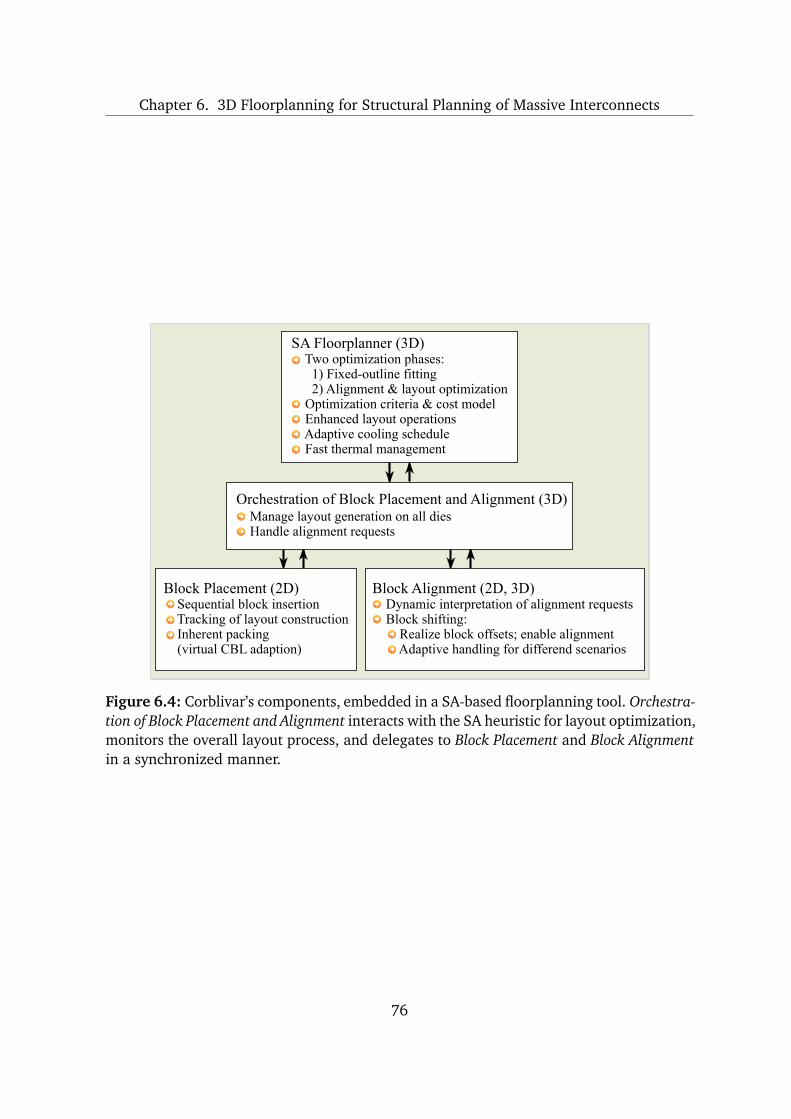
Chapter 6. 3D Floorplanning for Structural Planning of Massive Interconnects
Orchestration of Block Placement and Alignment (3D) Manage layout generation on all dies Handle alignment requests
Block Alignment (2D, 3D) Dynamic interpretation of alignment requests Block shifting: Realize block offsets; enable alignment Adaptive handling for differend scenarios
Block Placement (2D) Sequential block insertion Tracking of layout construction Inherent packing (virtual CBL adaption)
SA Floorplanner (3D) Two optimization phases: 1) Fixed-outline fitting 2) Alignment & layout optimization Optimization criteria & cost model Enhanced layout operations Adaptive cooling schedule Fast thermal management
Figure 6.4: Corblivar’s components, embedded in a SA-based floorplanning tool. Orchestra-tion of Block Placement and Alignment interacts with the SA heuristic for layout optimization,monitors the overall layout process, and delegates to Block Placement and Block Alignmentin a synchronized manner.
76

Chapter 6. 3D Floorplanning for Structural Planning of Massive Interconnects
Alignment Types
Given a fixed offset, s j is to be placed ARx/AR y units to the right/top (ARx/AR y ≥ 0) or
to the left/bottom (ARx/AR y < 0) of si, respectively, w.r.t. the blocks’ lower-left corners.
Fixed-offset alignment is required for restricted placement, e.g., of blocks with fixed pins.
For a (per definition positive) minimal overlap, the projected intersection of blocks si
and s j must be at least ARx units wide and/or AR y units high. The idea of such alignment
is to ensure overall straight but locally flexible paths for subsequent bus routing and/or
placement of vertical interconnect structures.
An alignment request defining a maximal distance requires the center points of blocks
si and s j to be at most ARx/AR y units apart. This way, interconnect structures can be easily
limited in their length and/or width.
It may not be necessary to define a request for both x- and y-coordinates; we label the
unrestricted coordinates’ request simply as don’t care.
Dynamic Interpretation of Alignment Tuples
The introduced tuples can be utilized for both intra-die/inter-die alignment by assigning
related blocks to one common CBL (die) / separate CBLs (dies). In other words, the align-
ment encoding does not restrict blocks to particular dies, which preserves the floorplanner’s
capability for optimizing block-die assignments.
Definition of Tuples for Alignment of Multiple Blocks
For 3D-IC interconnects, implementing links among multiple blocks is an essential sce-
nario. Thus, let us assume the placement of blocks s1 . . . sn has to consider several, com-
bined alignment requests for interconnect planning. The required set of tuples can
be derived in any desired fashion. For example, for requests requiring one reference
block s1 (e.g., to represent one specific end of a bus), the tuples would be defined as
s1, s2,
ARx2, ARTx2
,
AR y2, ARTy2
, . . . . . . . . . . . . . . ,
s1, sn,
ARxn, ARTxn
,
AR yn, ARTyn
.
To give another example, we can encode alignments in a chain-like fashion to enable
flexible interconnect structures (i.e., with local deviations from a straight, global path):
s1, s2,
ARx2, ARTx2
,
AR y2, ARTy2
,
s2, s3,
ARx3, ARTx3
,
AR y3, ARTy3
, . . . . . . . . . . . . . . ,
sn−1, sn,
ARxn, ARTxn
,
AR yn, ARTyn
.
77
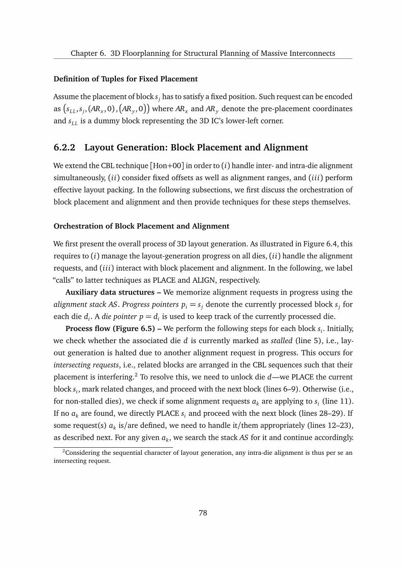
Chapter 6. 3D Floorplanning for Structural Planning of Massive Interconnects
Definition of Tuples for Fixed Placement
Assume the placement of block s j has to satisfy a fixed position. Such request can be encoded
as
sLL, s j, (ARx , 0) ,
AR y , 0
where ARx and AR y denote the pre-placement coordinates
and sLL is a dummy block representing the 3D IC’s lower-left corner.
6.2.2 Layout Generation: Block Placement and Alignment
We extend the CBL technique [Hon+00] in order to (i) handle inter- and intra-die alignment
simultaneously, (ii) consider fixed offsets as well as alignment ranges, and (iii) perform
effective layout packing. In the following subsections, we first discuss the orchestration of
block placement and alignment and then provide techniques for these steps themselves.
Orchestration of Block Placement and Alignment
We first present the overall process of 3D layout generation. As illustrated in Figure 6.4, this
requires to (i)manage the layout-generation progress on all dies, (ii) handle the alignment
requests, and (iii) interact with block placement and alignment. In the following, we label
“calls” to latter techniques as PLACE and ALIGN, respectively.
Auxiliary data structures – We memorize alignment requests in progress using the
alignment stack AS. Progress pointers pi = s j denote the currently processed block s j for
each die di. A die pointer p = di is used to keep track of the currently processed die.
Process flow (Figure 6.5) – We perform the following steps for each block si. Initially,
we check whether the associated die d is currently marked as stalled (line 5), i.e., lay-
out generation is halted due to another alignment request in progress. This occurs for
intersecting requests, i.e., related blocks are arranged in the CBL sequences such that their
placement is interfering.2 To resolve this, we need to unlock die d—we PLACE the current
block si, mark related changes, and proceed with the next block (lines 6–9). Otherwise (i.e.,
for non-stalled dies), we check if some alignment requests ak are applying to si (line 11).
If no ak are found, we directly PLACE si and proceed with the next block (lines 28–29). If
some request(s) ak is/are defined, we need to handle it/them appropriately (lines 12–23),
as described next. For any given ak, we search the stack AS for it and continue accordingly.
2Considering the sequential character of layout generation, any intra-die alignment is thus per se anintersecting request.
78

Chapter 6. 3D Floorplanning for Structural Planning of Massive Interconnects
1: p← d1 ▷ start w.l.o.g. on bottom die2: pi ← s1
3: loop4: si ← pi ← p5: if die d ← p is stalled then6: PLACE(si)7: mark si in any ai′ ∈ A as placed8: mark d as not stalled9: pi ← pi+1
10: else ▷ d is not stalled11: if some ak are defined for si then12: for all ak do ▷ consider ak w/ placed blocks first13: if ak in AS then14: ALIGN(ak)15: remove ak from AS16: mark si, s j in any ai′ ∈ A as placed17: mark d j = die
s j
as not stalled18: else19: add ak to AS20: mark d as stalled21: p← die
s j
22: end if23: end for ▷ all ak considered24: if d is not stalled then25: pi ← pi+1
26: end if27: else ▷ no ak defined for si
28: PLACE(si)29: pi ← pi+1
30: end if31: end if ▷ si processed32: if pi = end then33: if some p j = end then34: p← p j
35: else36: return done37: end if38: end if39: end loop
Figure 6.5: Orchestration of block placement and alignment.
79

Chapter 6. 3D Floorplanning for Structural Planning of Massive Interconnects
• If ak is found, it was previously handled while processing s j, the block to be aligned
with si. Thus, it is assured that preceding blocks on both related dies are placed
at this point. We can now safely ALIGN si and s j, mark them as placed, and drop
the request ak (lines 14–17). Note that only in cases where all requests for si are
handled, we proceed on the current die d (line 25). Otherwise, we continue layout
generation without loss of generality (w.l.o.g.) on s j ’s die d ′ (line 21).
• If ak is not found in AS, s j was not processed yet. We then memorize ak as in progress,
halt layout generation on d, and continue on d ′ (lines 19–21).
Finally, if layout generation is done on d, we proceed on yet unfinished dies until the whole
3D-IC layout is generated (lines 32–38).
Be aware that deadlock situations, i.e., layout generation on different dies is waiting
for each other until particular blocks can be aligned, cannot occur due to resolving of
stalled dies. This is true for any valid alignment request; see also the subsection on block
alignment for related implications.
Block Placement
To maintain a valid layout during placement, it is necessary to consider previously placed
blocks. We propose a technique which allows us to (i) efficiently keep track of relevant
blocks, (ii) fix CBL tuples w.r.t. exceeding T-junctions, and (iii) virtually adapt CBL tuples
for layout compaction. Our approach differs from [Hon+00] in these features but follows
the same principle of sequential block placement.
Auxiliary data structures – We keep track of placed blocks using two stacks H j/Vj for
each CBL j. More precisely, these stacks are governed to contain CBL j ’s blocks currently
covering the vertical right / horizontal upper front of die d j; these are considered as the
boundary fronts for further placement.
Placement flow (Figure 6.6) – We determine each blocks’ si ∈ S j lower-left coordinates
(x i, yi) as follows (see Figure 6.7 for an example). First, we retrieve t i+1 previously placed
blocks from the respective stacks H j/Vj (line 3/20). These blocks are referred to as relevant
blocks in the following steps. Note that in cases where only tmax < t i+1 blocks are available,
the related CBL tuple is technically infeasible [Hon+00]. To fix such invalid tuples, we
simply consider all tmax blocks in order to fulfill the desired covering of T-junctions as best
as possible. Second, we determine si ’s y/x-coordinate—i.e., the coordinate orthogonal to
80

Chapter 6. 3D Floorplanning for Structural Planning of Massive Interconnects
1: b← ; ▷ set of relevant blocks2: if li = 1 then ▷ horizontal placement3: b←min
(t i + 1) ,
H j
× pop
H j
4: if H j = ; then5: si.l l.y ← 06: else7: si.l l.y ←min (b′.l l.y | b′ ∈ b)8: end if9: si.ur.y ← si.l l.y + si.height
10: si.l l.x ←max
b′.ur.x | [placed b′ ∈ S j]∗ ∧ si, b′ intersect in y-axis
11: si.ur.x ← si.l l.x + si.wid th12: if ∄(b′ ∈ b | si.ur.y ≤ b′.l l.y) then13: push(Vj, si)14: end if15: push(H j, si)16: for all b′ ∈ b | b′ not left of si do17: push
H j, b′
18: end for19: else ▷ vertical placement20: b←min
(t i + 1) , |Vj|
× pop(Vj)21: if Vj = ; then22: si.l l.x ← 023: else24: si.l l.x ←min(b′.l l.x | b′ ∈ b)25: end if26: si.ur.x ← si.l l.x + si.wid th27: si.l l.y ←max
b′.ur.y | [placed b′ ∈ S j]∗ ∧ si, b′ intersect in x-axis
28: si.ur.y ← si.l l.y + si.height29: if ∄(b′ ∈ b | si.ur.x ≤ b′.l l.x) then30: push
H j, si
31: end if32: push
Vj, si
33: for all b′ ∈ b | b′ not below of si do34: push
Vj, b′
35: end for36: end if∗ Can be replaced by b′ ∈ b in case no alignment requests are given for the whole layout,i.e., no shifted blocks have to be considered.
Figure 6.6: Algorithm for block placement and related determination of coordinates.
81
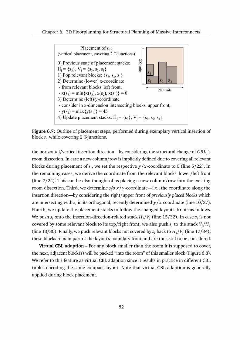
Chapter 6. 3D Floorplanning for Structural Planning of Massive Interconnects
s3s1
s4
s2
200 units
200 units
0) Previous state of placement stacks:Hj = s3, Vj = s3, s2, s11) Pop relevant blocks: s3, s2, s12) Determine (lower) x-coordinate - from relevant blocks' left front; - x(s4) = minx(s3), x(s2), x(s1) = 03) Determine (left) y-coordinate - consider in x-dimension intersecting blocks' upper front; - y(s4) = maxy(s1) = 454) Update placement stacks: Hj = s3, Vj = s3, s2, s4
Placement of s4 :(vertical placement, covering 2 T-junctions)
Figure 6.7: Outline of placement steps, performed during exemplary vertical insertion ofblock s4 while covering 2 T-junctions.
the horizontal/vertical insertion direction—by considering the structural change of CBL j ’s
room dissection. In case a new column/row is implicitly defined due to covering all relevant
blocks during placement of si, we set the respective y/x-coordinate to 0 (line 5/22). In
the remaining cases, we derive the coordinate from the relevant blocks’ lower/left front
(line 7/24). This can be also thought of as placing a new column/row into the existing
room dissection. Third, we determine si ’s x/y-coordinate—i.e., the coordinate along the
insertion direction—by considering the right/upper front of previously placed blocks which
are intersecting with si in its orthogonal, recently determined y/x-coordinate (line 10/27).
Fourth, we update the placement stacks to follow the changed layout’s fronts as follows.
We push si onto the insertion-direction-related stack H j/Vj (line 15/32). In case si is not
covered by some relevant block to its top/right front, we also push si to the stack Vj/H j
(line 13/30). Finally, we push relevant blocks not covered by si back to H j/Vj (line 17/34);
these blocks remain part of the layout’s boundary front and are thus still to be considered.
Virtual CBL adaption – For any block smaller than the room it is supposed to cover,
the next, adjacent block(s) will be packed “into the room” of this smaller block (Figure 6.8).
We refer to this feature as virtual CBL adaption since it results in practice in different CBL
tuples encoding the same compact layout. Note that virtual CBL adaption is generally
applied during block placement.
82
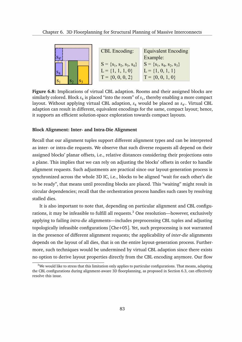
Chapter 6. 3D Floorplanning for Structural Planning of Massive Interconnects
s3s1
s4
s2
s4'
CBL Encoding:
S = s1, s2, s3, s4L = 1, 1, 1, 0T = 0, 0, 0, 2
Equivalent EncodingExample:S = s1, s4, s2, s3L = 1, 0, 1, 1T = 0, 0, 1, 0
Figure 6.8: Implications of virtual CBL adaption. Rooms and their assigned blocks aresimilarly colored. Block s4 is placed “into the room” of s1, thereby enabling a more compactlayout. Without applying virtual CBL adaption, s4 would be placed as s4′ . Virtual CBLadaption can result in different, equivalent encodings for the same, compact layout; hence,it supports an efficient solution-space exploration towards compact layouts.
Block Alignment: Inter- and Intra-Die Alignment
Recall that our alignment tuples support different alignment types and can be interpreted
as inter- or intra-die requests. We observe that such diverse requests all depend on their
assigned blocks’ planar offsets, i.e., relative distances considering their projections onto
a plane. This implies that we can rely on adjusting the blocks’ offsets in order to handle
alignment requests. Such adjustments are practical since our layout-generation process is
synchronized across the whole 3D IC, i.e., blocks to be aligned “wait for each other’s die
to be ready”, that means until preceding blocks are placed. This “waiting” might result in
circular dependencies; recall that the orchestration process handles such cases by resolving
stalled dies.
It is also important to note that, depending on particular alignment and CBL configu-
rations, it may be infeasible to fulfill all requests.3 One resolution—however, exclusively
applying to failing intra-die alignments—includes preprocessing CBL tuples and adjusting
topologically infeasible configurations [Che+05]. Yet, such preprocessing is not warranted
in the presence of different alignment requests; the applicability of inter-die alignments
depends on the layout of all dies, that is on the entire layout-generation process. Further-
more, such techniques would be undermined by virtual CBL adaption since there exists
no option to derive layout properties directly from the CBL encoding anymore. Our flow
3We would like to stress that this limitation only applies to particular configurations. That means, adaptingthe CBL configurations during alignment-aware 3D floorplanning, as proposed in Section 6.3, can effectivelyresolve this issue.
83
Chapter 6. 3D Floorplanning for Structural Planning of Massive Interconnects
described below includes layout-aware techniques, i.e., enables alignment in some cases
of previously placed blocks.
Alignment flow – Remember that alignment tuples cover two blocks; requests spanning
more blocks/tuples are implicitly handled stepwise. Initially, we need to check whether one
or both blocks have been previously placed. As indicated, the latter occurs (i)when multiple
requests cover the same block(s), (ii) after resolving stalled dies due to intersecting request,
or (iii) for intra-die requests in general. Depending on preceding placement, the following
three scenarios are to be distinguished for handling request ak.
Scenario I, both blocks are placed – In this case, we cannot fulfill ak since we omit post-
placement shifting for the following reason. Based on our observations, shifting placed
blocks requires abutting and/or nearby blocks to be shifted as well in order to maintain
a valid layout. This is impractical in the presence of different alignment requests—such
shifting can then undermine handling of remaining requests and/or invalidate previously
processed ones.
Scenario II, one block is yet unplaced – Here, we assume w.l.o.g. that si ∈ ak is yet
unplaced and s j ∈ ak was previously placed. Depending on both the coordinates of placed
s j and the properties of ak, we may be able to fulfill ak as follows. First, we determine si ’s
y/x-coordinates orthogonal to its horizontal/vertical insertion direction (see “Second”
step of block placement). Next, based on both the inherent offset between si and s j and
the defined alignment of ak, we derive the required shifting range rsy
si, s j
/rsx
si, s j
,
i.e., the remaining offset of si w.r.t. s j in order to fulfill ak. Note that rs
si, s j
= −rs
s j, si
,
i.e., the shifting range is directed and invertible. In cases rs
si, s j
= 0, ak is already
fulfilled. In cases rs
si, s j
< 0, we would need to shift si downward/leftward which is
trivially prohibited while maintaining a valid and (due to virtual CBL adaption) packed
layout. Alternatively, we could shift placed s j upward/rightward; however, this is not
applicable, as mentioned before. (See also Figure 6.9 for an illustration.) Third, if and only
if rsy/x
si, s j
≥ 0, we can perform a corresponding forwards shift of si in y/x-direction
and thus satisfy ak’s partial request. Next, we perform above steps similarly for si ’s x/y-
coordinates along its insertion direction. Finally, we handle the placement stacks. In case
block shifting was conducted, we need to rebuild them. Therefore, the stacks’ current
blocks, along with si, are sorted by their coordinates in descending order; afterwards
uncovered (i.e., relevant) blocks redefine the stack. In case block shifting was not required,
we simply update the stacks, as described for block placement.
84
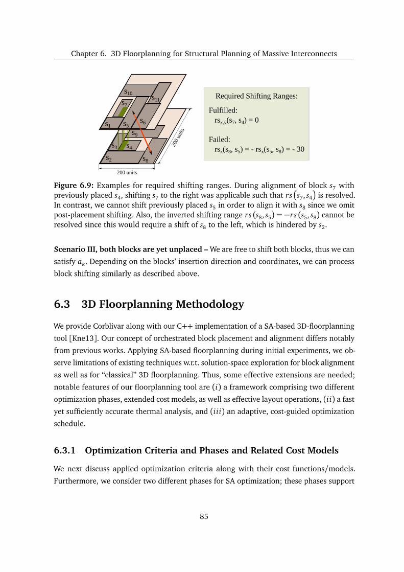
Chapter 6. 3D Floorplanning for Structural Planning of Massive Interconnects
s8s2
s3
200 units
s9
s4 200
units
Fulfilled: rsx,y(s7, s4) = 0
Failed: rsx(s8, s5) = - rsx(s5, s8) = - 30
Required Shifting Ranges:
s1 s5s6
s7
s10s11
Figure 6.9: Examples for required shifting ranges. During alignment of block s7 withpreviously placed s4, shifting s7 to the right was applicable such that rs
s7, s4
is resolved.In contrast, we cannot shift previously placed s5 in order to align it with s8 since we omitpost-placement shifting. Also, the inverted shifting range rs (s8, s5) = −rs (s5, s8) cannot beresolved since this would require a shift of s8 to the left, which is hindered by s2.
Scenario III, both blocks are yet unplaced – We are free to shift both blocks, thus we can
satisfy ak. Depending on the blocks’ insertion direction and coordinates, we can process
block shifting similarly as described above.
6.3 3D Floorplanning Methodology
We provide Corblivar along with our C++ implementation of a SA-based 3D-floorplanning
tool [Kne13]. Our concept of orchestrated block placement and alignment differs notably
from previous works. Applying SA-based floorplanning during initial experiments, we ob-
serve limitations of existing techniques w.r.t. solution-space exploration for block alignment
as well as for “classical” 3D floorplanning. Thus, some effective extensions are needed;
notable features of our floorplanning tool are (i) a framework comprising two different
optimization phases, extended cost models, as well as effective layout operations, (ii) a fast
yet sufficiently accurate thermal analysis, and (iii) an adaptive, cost-guided optimization
schedule.
6.3.1 Optimization Criteria and Phases and Related Cost Models
We next discuss applied optimization criteria along with their cost functions/models.
Furthermore, we consider two different phases for SA optimization; these phases support
85
Chapter 6. 3D Floorplanning for Structural Planning of Massive Interconnects
efficient solution-space exploration and layout optimization for 3D floorplanning with
block alignment. Each phase considers a subset of criteria, as discussed later on.
Outline
This criteria unifies evaluation of the layout’s bounding boxes, i.e., packing density, as well
as fixed-outline fitting. This is achieved by extending Chen and Chang’s aspect-ratio-based
cost model [CC06]. Our model is defined as
cOL = cPD + cARV
cPD = 12α
1+n f easible
n
×maxdi
Aoutl ine(b∈di)Aoutl ine(di)
cARV = 12α
1− n f easible
n
×maxdi
∆AR(di)2
∆AR (di) = ARoutl ine (b ∈ di)− ARoutl ine (di)
where cPD and cARV denote the respective cost terms for packing density and aspect-ratio
violation. Functions Aoutl ine and ARoutl ine determine the outline’s area and aspect ratio,
respectivly; both functions are determined w.r.t. a set of blocks b ∈ di / a die di. Note
that we perform cost calculation for previous n layout operations where n f easible ≤ n
operations resulted in a valid layout, i.e., blocks on all dies are fitting into the fixed outline.
Furthermore note that considering the respective maxima of both packing density and
aspect-ratio violation is critical; average values would be misleading the search in cases
where particular overflowing and fitting dies are compensating each others’ cost impact.
For n f easible = 0, cPD∝12α and cARV ∝
12α, which implies that cost functions guide the
SA search towards simultaneously increasing packing density and reducing aspect-ratio
violation. For n f easible = 1, cPD ∝ α and cARV = 0; only the packing density contributes
in case the SA search reached a solution-space region with only fitting layouts “nearby”.
Note that for best, fitting solutions, we determine cost with fixed n f easible = 1, i.e., we
temporarily ignore cost history to enable meaningful comparison of best solutions.
Alignment Mismatch
For an alignment tuple ak, we describe the spatial mismatch between desired alignment and
actual layout as cost cAM M (ak) =
rs
si, s j
(based on shifting ranges, Subsection 6.2.2).
For example, consider ak =
si, s j, (50,2), (0,−1)
where si and s j ’s center points are 100
86

Chapter 6. 3D Floorplanning for Structural Planning of Massive Interconnects
units apart w.r.t. the x-coordinate. Then, cAM M (ak) = 50. Overall cost is generally calculated
as cAM M =
ak∈A cAM M (ak).
Wirelength and TSV Count
We estimate wirelength based on the BB-2D3D-HPWL model introduced in Subsection 4.3.1.
However, since we refrain from placing TSVs explicitly during floorplanning, we consider
the related blocks’ outline—and terminal pins’ outline where applicable—for construction
of net bounding boxes. In order to account for wires connecting to TSV landing pads, we
also consider blocks on the upper die d j, j > i during construction of bounding boxes.
Partial estimation of wirelength for each net n on each corresponding die di, based on
these bounding boxes, is referred to as HPW L(n, di). Overall cost are then defined as
cW L =
n
lTSV × TSVs(n) +
di∈n HPW L (n, di)
cTSVs =
n TSVs(n)
where TSVs(n) denotes the required TSV count for net n. Note that we also account
for “TSV wirelength” lTSV in cW L. Also note that this model provides the most accurate
HPWL-based wirelength estimate without performing actual TSV placement, assuming
that TSVs can be subsequently placed into the nets’ bounding boxes.
Thermal Management
The optimization cost cT is defined by the estimated maximum temperature of the critical die
furthest away from the heatsink. Details on thermal analysis are given in Subsection 6.3.2.
SA Optimization Phase I, “Fixed-Outline Fitting”
The cost function is defined as cI = cOL. Note that we do not perform alignment in this
phase. The reason for initially focusing SA’s search solely on the fixed outline is simply that
non-fitting layouts are a “knock-out” criterion, regardless of any achieved block alignment
and layout optimization. The transition to Phase II is made when the SA search triggers
the first valid, i.e., fixed-outline-fitting layout.
87
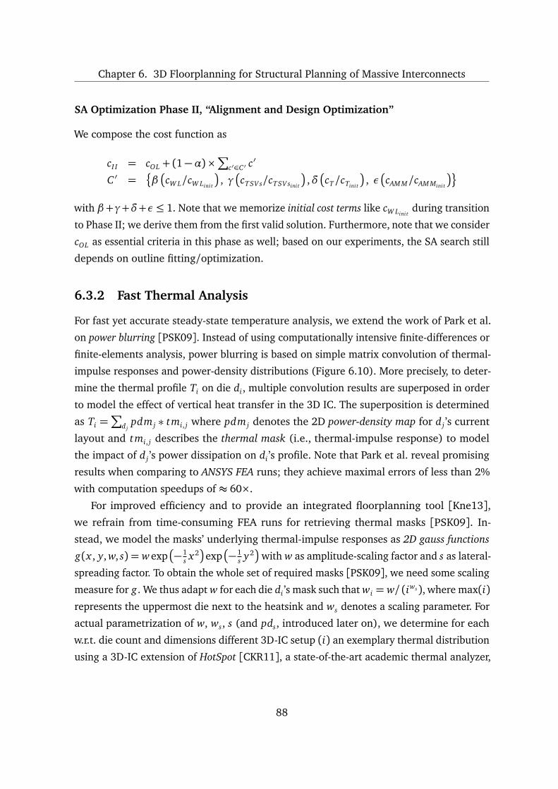
Chapter 6. 3D Floorplanning for Structural Planning of Massive Interconnects
SA Optimization Phase II, “Alignment and Design Optimization”
We compose the cost function as
cI I = cOL + (1−α)×
c′∈C ′ c′
C ′ =
β
cW L/cW Lini t
, γ
cTSVs/cTSVsini t
,δ
cT/cTini t
, ε
cAM M/cAM Mini t
with β+γ+δ+ε≤ 1. Note that we memorize initial cost terms like cW Lini tduring transition
to Phase II; we derive them from the first valid solution. Furthermore, note that we consider
cOL as essential criteria in this phase as well; based on our experiments, the SA search still
depends on outline fitting/optimization.
6.3.2 Fast Thermal Analysis
For fast yet accurate steady-state temperature analysis, we extend the work of Park et al.
on power blurring [PSK09]. Instead of using computationally intensive finite-differences or
finite-elements analysis, power blurring is based on simple matrix convolution of thermal-
impulse responses and power-density distributions (Figure 6.10). More precisely, to deter-
mine the thermal profile Ti on die di, multiple convolution results are superposed in order
to model the effect of vertical heat transfer in the 3D IC. The superposition is determined
as Ti =
d jpdm j ∗ tmi, j where pdm j denotes the 2D power-density map for d j ’s current
layout and tmi, j describes the thermal mask (i.e., thermal-impulse response) to model
the impact of d j ’s power dissipation on di ’s profile. Note that Park et al. reveal promising
results when comparing to ANSYS FEA runs; they achieve maximal errors of less than 2%
with computation speedups of ≈ 60×.
For improved efficiency and to provide an integrated floorplanning tool [Kne13],we refrain from time-consuming FEA runs for retrieving thermal masks [PSK09]. In-
stead, we model the masks’ underlying thermal-impulse responses as 2D gauss functions
g(x , y, w, s) = w exp
−1s x2
exp
−1s y2
with w as amplitude-scaling factor and s as lateral-
spreading factor. To obtain the whole set of required masks [PSK09], we need some scaling
measure for g. We thus adapt w for each die di ’s mask such that wi = w/ (iws), where max(i)represents the uppermost die next to the heatsink and ws denotes a scaling parameter. For
actual parametrization of w, ws, s (and pds, introduced later on), we determine for each
w.r.t. die count and dimensions different 3D-IC setup (i) an exemplary thermal distribution
using a 3D-IC extension of HotSpot [CKR11], a state-of-the-art academic thermal analyzer,
88
Chapter 6. 3D Floorplanning for Structural Planning of Massive Interconnects
Temperature Map for Die 1
Die 1
Die 2
Die n
... ... ... ... ... ...
Die 1
Die 2
Die n
+Superposition
Thermal-Impulse ResponsePower-Density Map
Models (very small) impact of inDie n dissipated power on
thermal profile in Die 1*Convolution
Models (small) impact of inDie 2 dissipated power on
thermal profile in Die 1
Thermal-Impulse ResponsePower-Density Map
*Convolution
Models (large) impact of inDie 1 dissipated power on
thermal profile in Die 1
Thermal-Impulse ResponsePower-Density Map
*Convolution
Figure 6.10: Power-blurring approach for thermal analysis. Given are a set of power-density maps and thermal-impulse responses. The latter describe how heat spreads fromvirtual power (point) sources placed within different dies; thus, they model the overall heatconduction within a 3D IC. Each power-density map is to be convoluted with the relatedthermal-impulse response. The superposition of these convolution results provides thetemperature map for a particular die. Note that the (partial) floorplans are contained withinthe white rectangles of the power-density maps; each map itself is padded, i.e., extendedfor means of estimation-error compensation and efficient convolution implementation.
89
Chapter 6. 3D Floorplanning for Structural Planning of Massive Interconnects
and (ii) a best fit for above parameters based on a local search using HotSpot’s solution as
reference model.
The gauss function g can be easily separated, i.e., substituted by a 1D functions’ product
gx × g y where gx(w, x , s) =p
w exp
−1s x2
and g y(w, y, s) =p
w exp
−1s y2
. For separa-
ble functions defining a matrix of size n×n, performing two subsequent and orthogonal 1D
convolutions is on par with 2D convolution [Ahn05]. By applying the first approach, how-
ever, we can decrease required operations from n2 to 2n [Ahn05]. For initial experiments
with n = 9, we observed a speedup of ≈ 4× while applying separated 1D convolutions
compared to a full 2D convolution.
As explained in Park et al.’s study [PSK09], we require some means of error com-
pensation for thermal estimation nearby die boundaries. We realize this by introducing
power-density padding zones, i.e., we extend the power-density maps with a “ring” of ⌊n/2⌋additional bins whose values are derived from blocks abutting the die boundaries (Fig-
ure 6.10). Additionally, these bins’ values are weighted with a scaling factor pds. It is
important to note that these bins are not extending the actual layout but only effect the
power-density matrix itself. This approach has two benefits: (i) the error compensation
can be flexibly tuned via pds and is thus adaptable to different 3D-IC setups, and (ii) calcu-
lation of the convolution itself is freed from consistently checking if bins are within defined
matrix boundaries. Since the latter checks are required for innermost loops, their omission
is expected to reduce runtime notably [Ahn05]; in initial experiments, we observed a
speedup of ≈ 3.5×.
6.3.3 Layout Operations
We consider the following set of layout operations to support the SA heuristic in effective
exploration of Corblivar’s solution space:
• swapping blocks within CBL sequences (i.e., dies),
• swapping blocks across CBL sequences,
• swapping or moving whole CBL tuples within CBL sequences,
• swapping or moving whole CBL tuples across CBL sequences,
• switching a block’s insertion direction,
• switching a block’s T-junctions,
• rotating hard blocks, and
• guided shaping of soft blocks as proposed in [CC06].
90
Chapter 6. 3D Floorplanning for Structural Planning of Massive Interconnects
Note that swap and move operations are subject to power-density constraints. Specifically,
we maintain a fixed block-die assignment, i.e., partitioning, such that blocks with highest
power consumption remain in the die nearest to the heatsink. During initial experiments,
this straightforward measure has proven as crucial for thermal management.
For optimization Phase I, blocks / CBL tuples and operations are selected randomly.
In Phase II, particularly blocks corresponding with failed alignment requests are selected.
They are swapped with adjacent blocks such that
rs(si, s j)
is reduced, i.e., such that the
alignment is more likely to be fulfilled.
6.3.4 Adaptive Optimization Schedule
As indicated earlier, we require an adaptive cooling schedule for improved efficiency of
solution-space exploration. Our schedule is capable of (i) guiding the SA search within
the two optimization phases and (ii) escaping local minima.
We determine the initial SA-temperature T0 by calculating the standard deviation of
Phase-I costs σ (cI), after stepwise application of some layout operations. Then, we set
T0 ≈ σ (ci) [SM91]. As for classical SA, applied operations are probabilistically accepted
in case of
rand[0..1]≤ exp−∆c/Ti
where ∆c is the layout’s cost difference after applying
a particular operation. Furthermore, Ti represents the current SA-temperature.
We next present the schedule’s three phases along with their temperature model. Note
that i labels the current step of imax total cooling steps.
Phase “Adaptive Cooling”
We apply this cooling phase during SA-Phase I, which is aiming for fixed-outline fitting.
Ti+1 =
c f1 +i−1
imax−1 × (c f2 − c f1)
× Ti
Given that c f1 < c f2 < 1.0, the cooling rate slows down. Here, the intention is to
achieve initially fast cooling for the global scope, followed by slower cooling in a confined,
“local” solution space.
Phase “Reheating and Freezing”
This is applied for SA Phase II, i.e., after a fitting layout was found in step i f irst .
Ti+1 =
1− i−i f irst
imax−i f irst
× c f3 × Ti
91
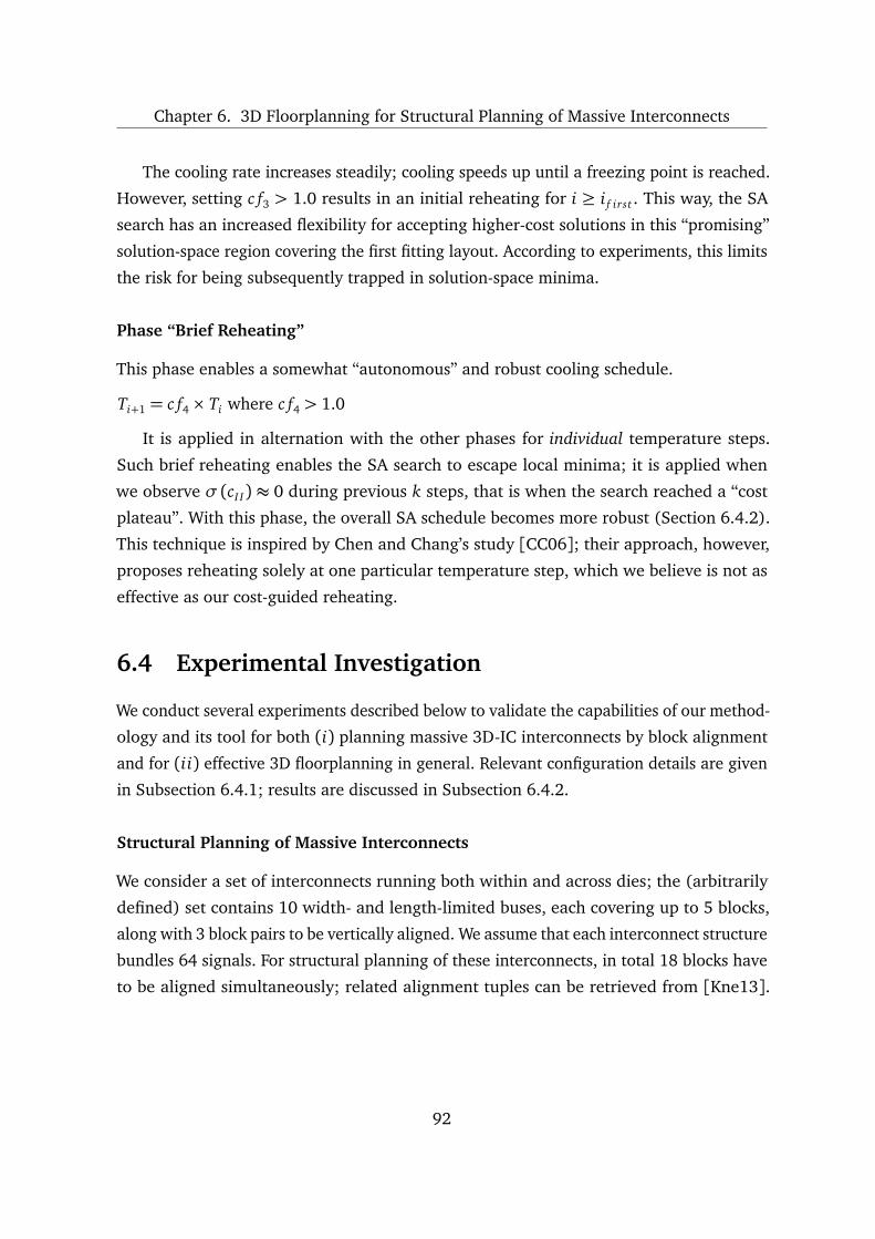
Chapter 6. 3D Floorplanning for Structural Planning of Massive Interconnects
The cooling rate increases steadily; cooling speeds up until a freezing point is reached.
However, setting c f3 > 1.0 results in an initial reheating for i ≥ i f irst . This way, the SA
search has an increased flexibility for accepting higher-cost solutions in this “promising”
solution-space region covering the first fitting layout. According to experiments, this limits
the risk for being subsequently trapped in solution-space minima.
Phase “Brief Reheating”
This phase enables a somewhat “autonomous” and robust cooling schedule.
Ti+1 = c f4 × Ti where c f4 > 1.0
It is applied in alternation with the other phases for individual temperature steps.
Such brief reheating enables the SA search to escape local minima; it is applied when
we observe σ (cI I) ≈ 0 during previous k steps, that is when the search reached a “cost
plateau”. With this phase, the overall SA schedule becomes more robust (Section 6.4.2).
This technique is inspired by Chen and Chang’s study [CC06]; their approach, however,
proposes reheating solely at one particular temperature step, which we believe is not as
effective as our cost-guided reheating.
6.4 Experimental Investigation
We conduct several experiments described below to validate the capabilities of our method-
ology and its tool for both (i) planning massive 3D-IC interconnects by block alignment
and for (ii) effective 3D floorplanning in general. Relevant configuration details are given
in Subsection 6.4.1; results are discussed in Subsection 6.4.2.
Structural Planning of Massive Interconnects
We consider a set of interconnects running both within and across dies; the (arbitrarily
defined) set contains 10 width- and length-limited buses, each covering up to 5 blocks,
along with 3 block pairs to be vertically aligned. We assume that each interconnect structure
bundles 64 signals. For structural planning of these interconnects, in total 18 blocks have
to be aligned simultaneously; related alignment tuples can be retrieved from [Kne13].
92
Chapter 6. 3D Floorplanning for Structural Planning of Massive Interconnects
Such scenario has not been considered in previous studies, thus we cannot meaningfully
compare to other work.4
Regular and Large-Scale 3D Floorplanning
To evaluate Corblivar’s efficiency w.r.t. key 3D floorplanning objectives, we look into layout
packing, wirelength reduction5, and thermal optimization. We compare our work to relevant
previous studies [Che10; Zho+07]. Furthermore, we demonstrate Corblivar’s scalability
by utilizing the IBM-HB+ benchmark suite [Ng+06]. To the best of our knowledge, this is
the first time that these large-scale circuits are considered for 3D floorplanning.
6.4.1 Configuration
3D-IC Configuration and Benchmarks
We assume F2B-stacking of two or three dies. Dies are 100µm thick; further properties
are given in [Kne13]. Terminal pins are only available on the lowermost die which is
assumed to be connected to the package board. Practical (i.e., stackable) fixed outlines
are ranging from 10mm× 10mm up to 15mm× 15mm. We consider GSRC [GSRC00] and
IBM-HB+ [Ng+06] circuits. For reasonable utilization of die outlines, benchmarks are
enlarged. In this context, power-density values are scaled down by factor 10. Also, results
are referring to packed layouts where feasible; reduced outlines are reported. Deadspace
utilization by 10µm×10µm-sized TSVs was negligible in most cases, we thus refrain from
optimizing and reporting TSV counts.
4Previous studies on block alignment for 3D ICs have looked into differing scenarios. Nain andChrzanowska-Jeske [NC11] propose techniques to split up and align modules among adjacent dies withzero offsets. They neglect to provide derived benchmarks containing split-up blocks, thus a comparisonis hindered. Law et al. [LYC06] consider a more flexible problem formulation; for vertical bus planning,they define sets of blocks for each die separately and require that at least one block from each set/die isvertically aligned with one block from the other sets/dies. This simplified problem is not compatible withour approach; we require that all specified blocks are to be aligned. Li et al. [LMH09] indicate capabilitiesfor block alignment, but refrain from providing further details and related experimental results. Finally, notethat all aforementioned studies consider only inter-die alignment with fixed offsets. In contrast, we enableinter-die as well as intra-die alignment, both with fixed and/or flexible offsets.
5We neglect to derive alignment tuples from the considered benchmarks’ nets. In other words, we do notapply block alignment for planning of “regular-sized” signal interconnects.
93

Chapter 6. 3D Floorplanning for Structural Planning of Massive Interconnects
Table 6.1: Results on enlarged GSRC benchmarks for applied interconnect planning, i.e.,block alignment (upper part), compared to results for floorplanning without interconnectplanning (lower part).
2 Dies 3 Dies
Metric n100 n200 n300 n100 n200 n300
Wirelength
cm× 103
1.18 1.81 1.97 1.10 1.93 2.07
Die Outlines
cm2
1.14 1.14 1.14 0.73 0.84 0.91
Total Deadspace (%) 29.21 30.39 31.14 26.81 37.20 42.06
Runtime (s) 80 359 891 81 360 858
Wirelength
cm× 103
1.83 2.60 2.53 1.34 2.59 2.76
Die Outlines
cm2
1.00 1.08 1.07 0.77 0.82 0.35
Total Deadspace (%) 18.82 27.04 26.39 29.81 36.00 32.19
Runtime (s) 59 304 726 59 304 734∗Estimated routing detours for (presumably) unaligned interconnect structures are included.
Experimental Setup
We conduct all experiments on a Intel Core 2 system; reported runtimes are thus comparable.
Corblivar and [Che10] are embedded in SA-based tools; best results are chosen from 5
up to 25 runs. Applied Corblivar parameters are retrievable from [Kne13]. For HotSpot,
default settings are applied [CKR11].
6.4.2 Results and Discussion
Structural Planning of Massive Interconnects
We observe that the entire set of interconnects is successfully integrated, i.e., all related
blocks can be simultaneously aligned (upper part of Table 6.1). Compared to experiments
where planning of interconnects is ignored (lower part of Table 6.1), we expect and observe
an increase of die outlines and deadspace—block alignment limits the flexibility of layout
packing. More importantly, however, we observe notable wirelength increases in case of
neglected interconnect planning; on average 35% routing detours arise from interconnects
embedded in unaligned blocks. Finally, fixed die outlines were fulfilled in any case, i.e.,
the proposed SA phases are effective. (Further discussion on the adaptive optimization
schedule is given at the end of this subsection.)
An example for successful interconnect planning is illustrated in Fig. 6.11.
94

Chapter 6. 3D Floorplanning for Structural Planning of Massive Interconnects
0
2000
4000
6000
0 2000 4000 6000 8000
8000
Width [µm]
Hei
ght [µ
m]
Legend
Block
Vertical bus
Via bus connected,aligned block
Classical bus
Figure 6.11: Successfully planned interconnect structures with corresponding block align-ment, for enlarged benchmark n100. For illustration purposes, we consider a reduced setof buses, covering nine blocks.
95
Chapter 6. 3D Floorplanning for Structural Planning of Massive Interconnects
Regular 3D Floorplanning
Next, we discuss results on floorplanning with applied layout packing and equally weighted
consideration of thermal and wirelength optimization (Table 6.2). We observe that Cor-
blivar is competitive with a force-directed tool [Zho+07] and superior to a SA-based
tool [Che10]; both represent state-of-the-art academic works. In particular, we achieve
comparable wirelengths and temperatures as [Zho+07] but with on average by 17.5%
reduced deadspace ratios. This indicates the efficiency of layout packing, which is most
likely achieved by the proposed virtual CBL adaption. Comparing to [Che10], however,
we note that Corblivar’s layouts exhibit on average 10% larger deadspace ratios and thus
reduced packing densities. Nonetheless, we achieve on average onto 80% reduced wire-
lengths. Also, the high packing density of [Che10] comes at a price; maximal temperatures
are notably increased by tens of Kelvins compared to Corblivar. Thus, our tool effectively
addresses the trade-off between packing density and maximum temperature. Furthermore,
fixed outlines were fulfilled in these experiments as well.
As for our temperature analysis, we observe that it shows some local deviations com-
pared to HotSpot-verification runs (Figure 6.12). As indicated in [PSK09], convolution-
based thermal analysis particularly induces estimation errors at die boundaries. Thanks to
our proposed mask parametrization, the actual thermal-distribution scale—i.e., the scale
w.r.t. HotSpot runs—is matched nevertheless. For analysis during layout optimization, i.e.,
maximal-temperatures estimation, our approach is sufficiently accurate and thus applica-
ble. It is also efficient due to fast computation; one run can be conducted in ≈ 20ms. For
comparison, one HotSpot run can take tens of seconds up to a few minutes.
Large-Scale 3D Floorplanning
The IBM-HB+ suite does not include power information; we thus restricted Corblivar
to wirelength and packing optimization, with successful application of fixed-outline con-
straints. Results on arbitrarily selected and enlarged circuits are provided in Table 6.3.
We observe that the overall deadspace amount for these experiments is on average larger
than for experiments on some GSRC circuits. This is expected and likely due to the fact
that IBM-HB+ circuits contain up to ≈ 1, 500 blocks where largest blocks are ≈ 33, 000×bigger than smallest ones; such designs are difficult to floorplan [Roy+09]. Nevertheless,
considering that deadspace results for these highly-irregular and large-scale circuits are
96

Chapter 6. 3D Floorplanning for Structural Planning of Massive InterconnectsTa
ble
6.2:
Com
para
tive
resu
lts
onG
SRC
benc
hmar
ksfo
rla
yout
pack
ing
wit
hth
erm
alan
dw
irel
engt
hop
tim
izat
ion.
Ben
chm
arks
are
not
enla
rged
for
fair
com
pari
son.
Cor
bliv
ar,2
Die
sC
orbl
ivar
,2D
ies
Met
ric
n100
n200
n300
Avg
ami3
3xe
rox
Avg
Wir
elen
gth
µm×
105
3.70
6.57
9.07
6.45
2.02
13.8
97.
96D
ieO
utlin
es
µm
2×
105
1.01
0.99
1.61
1.20
10.3
814
3.15
76.7
7To
talD
eads
pace
(%)
11.9
812
.01
15.6
513
.21
44.3
132
.41
38.3
6M
axTe
mp[C
KR
11]
(K
)31
3.81
314.
5331
5.95
314.
7630
9.14
353.
8533
1.49
Run
tim
e(s
)10
828
654
831
450
1432
[Zho+
07],
2D
ies
[Che
10],
2D
ies
Met
ric
n100
n200
n300
Avg
ami3
3xe
rox
Avg
Wir
elen
gth
µm×
105
3.65
6.18
9.53
6.45
1.81
17.1
49.
48D
ieO
utlin
es
µm
2×
105
1.19
1.21
2.15
1.52
9.65
125.
1767
.41
Tota
lDea
dspa
ce(%
)25
.02
27.8
736
.69
29.8
640
.09
22.7
031
.40
Max
Tem
p[C
KR
11]
(K
)31
3.31
313.
7431
4.63
313.
8933
6.36
366.
4835
1.42
Run
tim
e(s
)43
944
652
647
019
347
120
Cor
bliv
ar,3
Die
sC
orbl
ivar
,3D
ies
Met
ric
n100
n200
n300
Avg
ami3
3xe
rox
Avg
Wir
elen
gth
µm×
105
4.24
7.19
10.2
87.
242.
0616
.36
9.21
Die
Out
lines
µm
2×
105
0.75
0.68
1.08
0.84
8.98
117.
4863
.23
Tota
lDea
dspa
ce(%
)20
.53
14.6
216
.27
17.1
457
.08
45.0
951
.09
Max
Tem
p[C
KR
11]
(K
)35
5.62
363.
9436
3.35
360.
9733
3.17
416.
6137
4.89
Run
tim
e(s
)15
438
070
441
371
2247
[Zho+
07],
3D
ies
[Che
10],
3D
ies
Met
ric
n100
n200
n300
Avg
ami3
3xe
rox
Avg
Wir
elen
gth
µm×
105
4.59
7.17
10.6
17.
462.
2221
.86
12.0
4D
ieO
utlin
es
µm
2×
105
0.97
0.82
1.48
1.09
7.54
88.9
348
.24
Tota
lDea
dspa
ce(%
)38
.89
28.6
438
.65
35.3
948
.87
27.4
738
.17
Max
Tem
p[C
KR
11]
(K
)34
8.55
360.
6036
1.35
356.
8338
4.39
482.
1643
3.28
Run
tim
e(s
)26
649
757
444
619
348
121
97

Chapter 6. 3D Floorplanning for Structural Planning of Massive Interconnects
322
324
326
328
330
332
334
(a) (b)
Figure 6.12: Thermal maps of the critical die, i.e., the die furthest away from the heatsink,benchmark n300. The Kelvin-based temperature scale of our fast analysis (a) mostlymatches with the HotSpot-scale (b); yet, minor local deviations are recognizable.
Table 6.3: Results on IBM-HB+ benchmarks for packing and wirelength optimization.
2 Dies 3 Dies
Metric ibm01 ibm03 ibm07 ibm01 ibm03 ibm07
Wirelength
cm× 103
4.77 7.29 1.77 4.67 7.39 1.67
Die Outlines
cm2
0.64 0.65 0.79 0.46 0.48 0.57
Total Deadspace (%) 17.24 19.26 18.59 24.97 27.86 24.88
Runtime (s)∗ 1195 3611 3081 1285 3792 3895
on average better than results obtained by applying [Che10; Zho+07] on “regular-scale”
GSRC benchmarks, Corblivar’s scalability w.r.t. layout packing is successfully demonstrated.
Impact of the Adaptive Optimization Schedule
One drawback typically associated with SA is the task of appropriate cooling-schedule
parametrization, which in turn governs the solution-space exploration. Based on initial
experiments, we found this task to be especially challenging for our scenario of block
alignment; thus we proposed an adaptive schedule (Subsection 6.3.4). We observe that
its phases have positive impact on the solution-space exploration. For example, when
cost has not changed notably over the course of several cooling steps, the Phase “Brief
Reheating” is applied to escape a solution-space minima. This enables the search to
98
Chapter 6. 3D Floorplanning for Structural Planning of Massive Interconnects
1e-181e-161e-141e-121e-101e-081e-06
0.00010.01
1100
0 50 100 150 200 250 300 350 400 450 5000.4
0.5
0.6
0.7
0.8
0.9
1
SA
Tem
pera
ture
Norm
aliz
ed A
vg S
olu
tion C
ost
SA Step
Temperature and Cost Schedule - n100
SA Temperature
Avg Cost (Accepted Sol.) - SA Phase 1Best Cost - SA Phase 2
New Best Solution
A
B
C
Figure 6.13: Temperature-cost correlation, benchmark n100. “Brief Reheating” (A, C)enables to escape local minima while “Reheating and Freezing” (B) increases chances fortriggering new best solutions notably.
continue despite previously inadequate (e.g., too fast) cooling—the cooling schedule can
be considered robust (Figure 6.13, Regions A and C). Furthermore, after the first valid
(i.e., fixed-outline fitting) solution is found, the Phase “Reheating and Freezing” increases
chances for triggering new best solutions notably (Figure 6.13, Region B).
6.5 Summary and Conclusions
With the methodology and tool presented in this chapter, we extend 3D floorplanning
towards structural planning of interconnects—an important yet inadequately addressed
scenario for future highly-parallel, massively-interconnected 3D ICs.
To tackle this omission of previous works, we promote block alignment. We initially
discuss how 3D (inter-die) and 2D (intra-die) alignment can be applied for planning of
diverse interconnects, e.g., vertical buses connecting possibly split-up blocks on separate
dies, or classical 2D buses. We then introduce Corblivar, a 3D layout representation based
on an extended corner block list including novel alignment tuples. To this end, we also
develop effective techniques for block placement and alignment. We note that it is essential
99

Chapter 6. 3D Floorplanning for Structural Planning of Massive Interconnects
to synchronize alignment across the whole 3D IC—inter-die alignment requires to con-
sider each die’s layout in progress. Our techniques handle this appropriately for different
scenarios of blocks to be aligned and/or to be placed.
We embed Corblivar into an open-source, SA-based floorplanning tool. We also develop
necessitated extensions like adaptive SA cooling and convolution-based fast thermal anal-
ysis. Experimental results on GSRC and large-scale IBM-HB+ benchmarks demonstrate
Corblivar’s applicability for structural planning of interconnects as well as its competi-
tive performance for “classical” 3D floorplanning while considering fixed outlines, layout
packing, thermal management, and wirelength optimization.
100
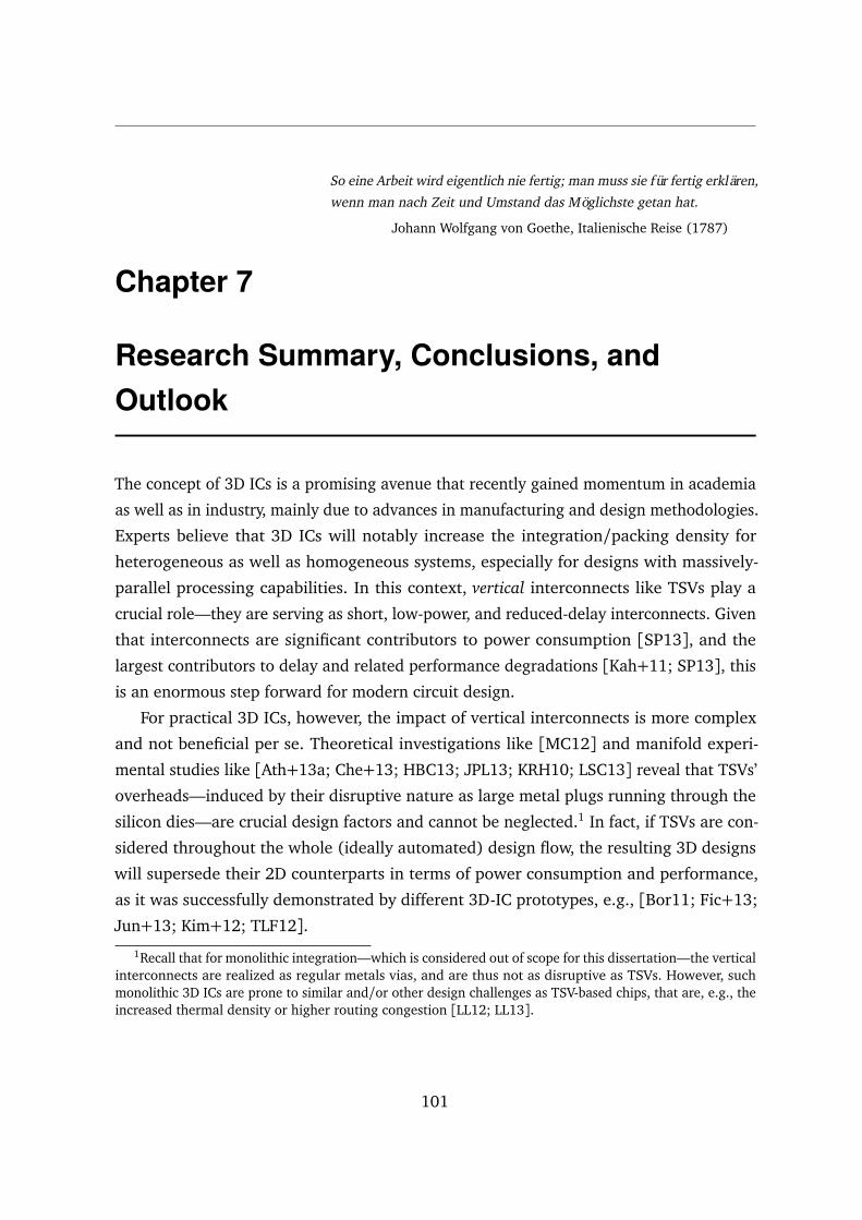
So eine Arbeit wird eigentlich nie fertig; man muss sie für fertig erklären,
wenn man nach Zeit und Umstand das Möglichste getan hat.
Johann Wolfgang von Goethe, Italienische Reise (1787)
Chapter 7
Research Summary, Conclusions, andOutlook
The concept of 3D ICs is a promising avenue that recently gained momentum in academia
as well as in industry, mainly due to advances in manufacturing and design methodologies.
Experts believe that 3D ICs will notably increase the integration/packing density for
heterogeneous as well as homogeneous systems, especially for designs with massively-
parallel processing capabilities. In this context, vertical interconnects like TSVs play a
crucial role—they are serving as short, low-power, and reduced-delay interconnects. Given
that interconnects are significant contributors to power consumption [SP13], and the
largest contributors to delay and related performance degradations [Kah+11; SP13], this
is an enormous step forward for modern circuit design.
For practical 3D ICs, however, the impact of vertical interconnects is more complex
and not beneficial per se. Theoretical investigations like [MC12] and manifold experi-
mental studies like [Ath+13a; Che+13; HBC13; JPL13; KRH10; LSC13] reveal that TSVs’
overheads—induced by their disruptive nature as large metal plugs running through the
silicon dies—are crucial design factors and cannot be neglected.1 In fact, if TSVs are con-
sidered throughout the whole (ideally automated) design flow, the resulting 3D designs
will supersede their 2D counterparts in terms of power consumption and performance,
as it was successfully demonstrated by different 3D-IC prototypes, e.g., [Bor11; Fic+13;
Jun+13; Kim+12; TLF12].1Recall that for monolithic integration—which is considered out of scope for this dissertation—the vertical
interconnects are realized as regular metals vias, and are thus not as disruptive as TSVs. However, suchmonolithic 3D ICs are prone to similar and/or other design challenges as TSV-based chips, that are, e.g., theincreased thermal density or higher routing congestion [LL12; LL13].
101
Chapter 7. Research Summary, Conclusions, and Outlook
Previous work on design automation for 3D ICs often neglects and/or oversimplifies the
cost and overhead introduced by vertical interconnects, especially during early phases like
floorplanning (Chapter 2). In contrast—and in compliance with more recent studies—we
advocate consistent consideration of vertical interconnects during the whole design process
for 3D chips. Specifically, we focus on interconnect planning and related design-quality
management during early design phases, as indicated in Chapter 3. An illustrative overview
of the dissertation’s contributions is given in Figure 7.1; in the remainder of this chapter,
we summarize and conclude our findings, and provide a corresponding outlook.
Research Summary and Conclusions
In the first part of this dissertation (Chapter 4), we address principles for interconnecting
pre-designed 2D blocks within new 3D-IC designs. In this context, we promote the use of
TSV islands, i.e., groups of TSVs. By reusing 2D blocks, we seek to enhance the transition
towards 3D integration in terms of limiting the needs for new, sophisticated 3D-EDA tools,
which are currently still in R&D stage. More importantly, even when such tools become
widely available, upgrading extensive IP portfolios appears too time- and cost-intensive.
An insight of our work is that many benefits provided by 3D ICs can be obtained while
reusing existing 2D blocks. Our proposed design style, placing TSV islands among IP-block-
reuse-based layouts, appears most promising and least risky for 3D-IC design in the next
few years.2 To enable our design style, we contribute novel techniques for net clustering
and TSV-island insertion. From the concept of spatial slacks, we derive techniques to insert
and redistribute deadspace. The resulting capabilities for deadspace management are an
important requirement for optimized placement of possibly large TSV islands in compact
layouts. Our techniques are bundled in a modular post-floorplanning process, which can
be easily integrated in existing design flows.
Experiments validate the feasibility and efficiency of our methodology. In this context,
however, we observe that TSV islands also come with some cost—initial experiments
revealed that naive algorithms may lead to high interconnect overhead of more than 30%.
The optimized techniques developed in the course of our research reduce this overhead
down to ≈ 9% for global block-level interconnects, making it tolerable, especially consid-
2It is important to note that this design style has been successfully applied by case studies like [Ath+13b;Jun+13; KTL12; ZL12]; thus it has proven as practically relevant and feasible.
102
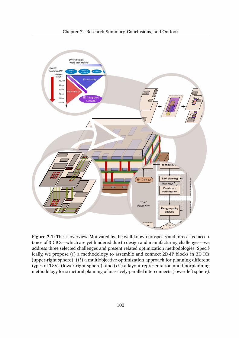
Chapter 7. Research Summary, Conclusions, and Outlook
Diversification:"More than Moore"
Scaling:"More Moore" Sensors
ActuatorsAnalog
RFBiochipsPhotonics
130 nm
90 nm
65 nm
45 nm
32 nm
22 nm
StandardCMOS
Performance
Functionality
3D IntegratedCircuits
Floorplanning
Design-qualityanalysis
3D-ICdesign flow
Methodologyconfiguration
Criteriasatisfied ?Yes No
Deadspaceoptimization
Globalloop
TSV planning
Placementetc.
3D-IC designMain loop
Figure 7.1: Thesis overview. Motivated by the well-known prospects and forecasted accep-tance of 3D ICs—which are yet hindered due to design and manufacturing challenges—weaddress three selected challenges and present related optimization methodologies. Specif-ically, we propose (i) a methodology to assemble and connect 2D-IP blocks in 3D ICs(upper-right sphere), (ii) a multiobjective optimization approach for planning differenttypes of TSVs (lower-right sphere), and (iii) a layout representation and floorplanningmethodology for structural planning of massively-parallel interconnects (lower-left sphere).
103

Chapter 7. Research Summary, Conclusions, and Outlook
ering that the majority of wires are running within blocks [SK00]. Thus, we successfully
enable the use of TSV islands within block-level-integrated 3D chips; such a process is
considered a prerequisite for high-quality physical design of 3D ICs.
The dissertation’s second part (Chapter 5) comprises a more comprehensive approach
for TSV planning. An important observation is that different types of TSVs have manifold
implications on design quality. Thus, we have to aim for a unified approach; our multiob-
jective design-optimization methodology can simultaneously place different types of TSVs
and evaluate their resulting impact on design quality. Notable aspects of our methodol-
ogy include (i) management of deadspace, the most critical and contested resource for
TSV placement, (ii) algorithms for planning different types of TSVs, and (iii) iterative
design-quality evaluation, enabling an appropriately guided optimization flow. Deadspace
management, in comparison to the first part of the dissertation, was extended to allow more
controlled deadspace manipulation. This was achieved by introducing shifting windows
and by exploiting the concept of constraint graphs. As in the first part of this disserta-
tion, the methodology is implemented as modular design-flow extension to be plugged in
parallel to or after floorplanning.
Experiments suggest that our methodology—with capabilities for planning of signal,
thermal, PG, and clock TSVs—can simultaneously optimize the interconnect distribution,
maximum temperature, estimated IR-drop, and clock-tree size. An important observation
is that this is enabled by quality-controlled interaction of TSV planning and deadspace
management. For general aspects of block-level 3D integration, we note that a greater
die count leads to greater TSV overhead and can subsequently undermine overall design
quality; this trend was not evident for solely planning of signal TSVs (Chapter 4). This
suggests to limit the die count for practical 3D ICs and, more importantly, indicates the need
for careful design-space exploration, i.e., the process of determining the chip architecture
and die specifications.
Besides explicit planning of single and/or grouped TSVs, we furthermore enable the
planning of massively-parallel interconnect structures, proposed in the last part of this
dissertation (Chapter 6). Future 3D ICs may rely on such large interconnect structures,
running between blocks spread among one and/or multiple dies. This is especially true for
3D ICs with massively-parallel processing capabilities—an emerging trend for 3D chips, as
already affirmed by prototypes like [Bor11; Fic+13; Kim+12]. We observe that structural
planning of such interconnects has been previously ignored during early design steps,
most likely impeding the interconnects’ routing in subsequent steps. Thus, we advocate
104
Chapter 7. Research Summary, Conclusions, and Outlook
integration of interconnect planning into 3D floorplanning. We realize this by means of
block alignment; 3D (inter-die) and 2D (intra-die) block alignment are applied for planning
of diverse interconnects, e.g., vertical buses interconnecting separate dies, or horizontal
buses running within dies. Our concept of flexible alignment encoding allows us to handle
several, differing bus configurations within one 3D IC. The encoding itself is wrapped into
an extended 3D layout representation, based on the well-known and efficient corner block
list. To this end, we also develop effective techniques for block placement, block alignment,
layout packing, as well as fast steady-state thermal analysis.
Initial experiments provide an important observation, namely that it is both essential
and feasible to synchronize alignment across the whole 3D IC. In particular, planning
vertical buses—with their inter-die alignment—requires to consider each die’s layout in
progress. Our developed techniques handle this appropriately for different scenarios of
block placement and alignment. For the implementation, we embed our methodology
into an open-source, SA-based floorplanning tool. Besides for planning of massive in-
terconnects, it has also proven competitive in other key objectives for 3D designs, e.g.,
thermal management and fixed-outline floorplanning. This is mainly achieved by elaborate
extensions like our cost-guided optimization schedule. In addition to the well-known
GSRC benchmarks, we apply large-scale IBM-HB+ benchmarks—for the first time in the
literature—for 3D floorplanning. Related results indicate that these designs mostly benefit
from increased die counts, in terms of reduced wirelength. Recalling other experiments
with GSRC benchmarks, where this was not necessarily the case, this finding suggests that
only large designs can obtain overall shorter interconnects by 3D-IC design.
Further findings and conclusions of this dissertation are given in the next chapter.
Research Outlook
This dissertation successfully addressed selected challenges w.r.t. interconnect planning in
3D ICs. The following outlook discusses possible further, related research directions.
As stated in Chapter 3, this dissertation’s focus is on early design phases. Thus, it was
out of scope, but appears interesting to extend and apply the proposed methodologies for a
more detailed physical-design flow, i.e., covering physical synthesis down to transistor and
wire layouts, as it was applied in other studies [Ath+13b; Jun+13; KTL12; LL10]. In this
context, it is important to note that our proposed methodologies address different steps of
105
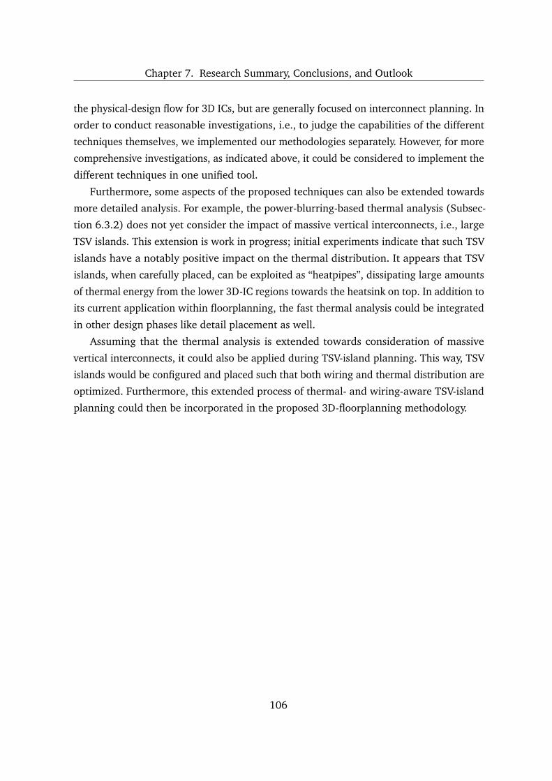
Chapter 7. Research Summary, Conclusions, and Outlook
the physical-design flow for 3D ICs, but are generally focused on interconnect planning. In
order to conduct reasonable investigations, i.e., to judge the capabilities of the different
techniques themselves, we implemented our methodologies separately. However, for more
comprehensive investigations, as indicated above, it could be considered to implement the
different techniques in one unified tool.
Furthermore, some aspects of the proposed techniques can also be extended towards
more detailed analysis. For example, the power-blurring-based thermal analysis (Subsec-
tion 6.3.2) does not yet consider the impact of massive vertical interconnects, i.e., large
TSV islands. This extension is work in progress; initial experiments indicate that such TSV
islands have a notably positive impact on the thermal distribution. It appears that TSV
islands, when carefully placed, can be exploited as “heatpipes”, dissipating large amounts
of thermal energy from the lower 3D-IC regions towards the heatsink on top. In addition to
its current application within floorplanning, the fast thermal analysis could be integrated
in other design phases like detail placement as well.
Assuming that the thermal analysis is extended towards consideration of massive
vertical interconnects, it could also be applied during TSV-island planning. This way, TSV
islands would be configured and placed such that both wiring and thermal distribution are
optimized. Furthermore, this extended process of thermal- and wiring-aware TSV-island
planning could then be incorporated in the proposed 3D-floorplanning methodology.
106
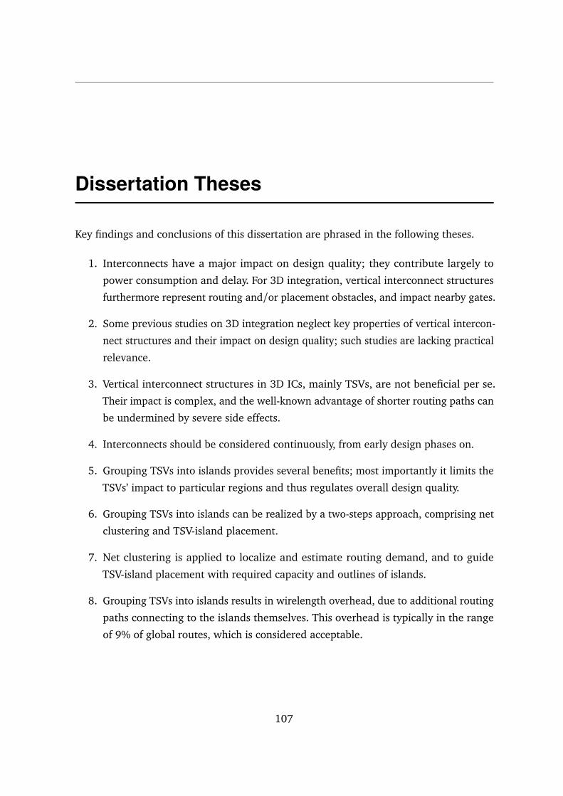
Dissertation Theses
Key findings and conclusions of this dissertation are phrased in the following theses.
1. Interconnects have a major impact on design quality; they contribute largely to
power consumption and delay. For 3D integration, vertical interconnect structures
furthermore represent routing and/or placement obstacles, and impact nearby gates.
2. Some previous studies on 3D integration neglect key properties of vertical intercon-
nect structures and their impact on design quality; such studies are lacking practical
relevance.
3. Vertical interconnect structures in 3D ICs, mainly TSVs, are not beneficial per se.
Their impact is complex, and the well-known advantage of shorter routing paths can
be undermined by severe side effects.
4. Interconnects should be considered continuously, from early design phases on.
5. Grouping TSVs into islands provides several benefits; most importantly it limits the
TSVs’ impact to particular regions and thus regulates overall design quality.
6. Grouping TSVs into islands can be realized by a two-steps approach, comprising net
clustering and TSV-island placement.
7. Net clustering is applied to localize and estimate routing demand, and to guide
TSV-island placement with required capacity and outlines of islands.
8. Grouping TSVs into islands results in wirelength overhead, due to additional routing
paths connecting to the islands themselves. This overhead is typically in the range
of 9% of global routes, which is considered acceptable.
107
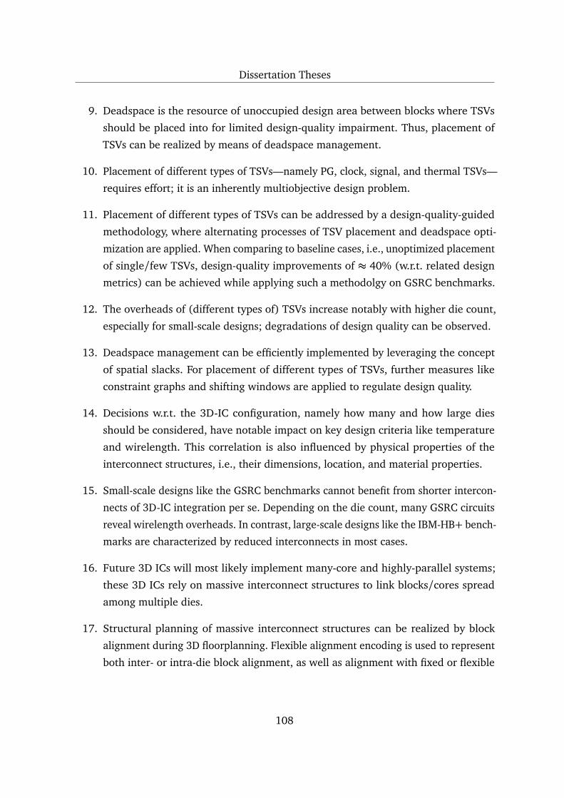
Dissertation Theses
9. Deadspace is the resource of unoccupied design area between blocks where TSVs
should be placed into for limited design-quality impairment. Thus, placement of
TSVs can be realized by means of deadspace management.
10. Placement of different types of TSVs—namely PG, clock, signal, and thermal TSVs—
requires effort; it is an inherently multiobjective design problem.
11. Placement of different types of TSVs can be addressed by a design-quality-guided
methodology, where alternating processes of TSV placement and deadspace opti-
mization are applied. When comparing to baseline cases, i.e., unoptimized placement
of single/few TSVs, design-quality improvements of ≈ 40% (w.r.t. related design
metrics) can be achieved while applying such a methodolgy on GSRC benchmarks.
12. The overheads of (different types of) TSVs increase notably with higher die count,
especially for small-scale designs; degradations of design quality can be observed.
13. Deadspace management can be efficiently implemented by leveraging the concept
of spatial slacks. For placement of different types of TSVs, further measures like
constraint graphs and shifting windows are applied to regulate design quality.
14. Decisions w.r.t. the 3D-IC configuration, namely how many and how large dies
should be considered, have notable impact on key design criteria like temperature
and wirelength. This correlation is also influenced by physical properties of the
interconnect structures, i.e., their dimensions, location, and material properties.
15. Small-scale designs like the GSRC benchmarks cannot benefit from shorter intercon-
nects of 3D-IC integration per se. Depending on the die count, many GSRC circuits
reveal wirelength overheads. In contrast, large-scale designs like the IBM-HB+ bench-
marks are characterized by reduced interconnects in most cases.
16. Future 3D ICs will most likely implement many-core and highly-parallel systems;
these 3D ICs rely on massive interconnect structures to link blocks/cores spread
among multiple dies.
17. Structural planning of massive interconnect structures can be realized by block
alignment during 3D floorplanning. Flexible alignment encoding is used to represent
both inter- or intra-die block alignment, as well as alignment with fixed or flexible
108

Dissertation Theses
offsets. Thus, any type of vertical buses (interconnecting dies) or classical horizontal
buses (running within dies), with fixed or flexible shapes, can be implemented.
18. Planning vertical buses, based on inter-die block alignment, requires to synchronize
the layout-generation process across all dies. Therefore, an orchestrated layout-
generation process is proposed.
19. Simulated annealing, applied for 3D floorplanning with means of block alignment,
can be improved by a cost-guided optimization schedule. Such a schedule increases
the SA-temperature in cases where local minima are triggered; the minima can sub-
sequently be escaped. Thus, higher-quality solutions can be found, and the schedule
is less prone to misconfiguration (e.g., by means of too fast cooling).
20. Omitting structural planning of massive interconnects can lead to notable routing
overheads. For example, even for small-scale GSRC benchmarks comprising only ten
buses, each bundling 64 wires, we observe an wirelength increase of up to ≈ 45%.
21. Thermal management is a critical task for 3D floorplanning; fast and sufficiently
accurate techniques are required for continuous thermal evaluation.
22. Fast thermal management can be realized by power blurring which is based on
matrix convolution of thermal-impulse responses and power-density distributions.
Power blurring can determine the temperature profiles of a 3D IC approximately
3, 000× faster than HotSpot, an acknowledged thermal-analysis tool. The accuracy
of power blurring and HotSpot are comparable; power blurring reveals only minor
temperature-profile deviations when compared to HotSpot.
23. Fast thermal management enables the 3D-floorplanning tool to effectively trade-off
temperature with other design criteria. For example, an area increase of ≈ 20% can
notably reduce temperatures by up to 60 Kelvin for GSRC benchmarks.
109

Notation
Abbreviations
3D
Three-Dimensional
B2B
Back-to-Back
BEOL
Back End of the Line
CBL
Corner Block List
CG
Constraint Graph
CMOS
Complementary Metal-Oxide-Semiconductor
D2D
Die-to-Die
D2W
Die-to-Wafer
DFT
Design for Testability
EDA
Electronic Design Automation
110

Notation
F2B
Face-to-Back
F2F
Face-to-Face
FEA
Finite Element Analysis
FEOL
Front End of the Line
HPWL
Half-Perimeter Wirelength
IC
Integrated Circuit
IP
Intellectual Property
ITRS
International Technology Roadmap for Semiconductors
KOZ
Keep-Out Zone
L2D
Legacy 2D Style
L2Di
Legacy 2D Style With TSV Islands
NoC
Network-on-Chip
PG
Power/Ground
111

Notation
R2D
Redesigned 2D Style
RDL
Redistribution Layer
SA
Simulated Annealing
SiP
System-in-Package
TSV
Through-Silicon Via
W2W
Wafer-to-Wafer
w.l.o.g.
Without Loss of Generality
w.r.t.
With Respect to
Selected Symbols (Sorted by Appearance)
D
A set of dies / chips / active layers.
d
A particular die.
(hd , wd)The height and width of a particular die.
B
A set of (rectangular) IP blocks.
112

Notation
b
A particular IP block.
(hb, wb)The height and width of a particular IP block.
P b
A set of pins for IP block b.
P
A set of boundary pins, connecting the chip with its periphery.
p
A particular pin.
δxp ,δ y
p
The pin p’s horizontal and vertical offset, with respect to the related block’s geometric
center.
N
A set of nets, also called netlist.
n
A particular net, which describes a connection between two or more pins.
T
A set of TSV islands.
t
A particular TSV island.
(ht , wt)The height and width of a particular TSV island.
κt
The capacity of a particular TSV island.
F
A 3D floorplan; each block b is assigned a location (xb, yb, db) such that no blocks
113

Notation
overlap, whereas the coordinate of the block’s origin is denoted as (xb, yb) and db
denotes the assigned die.
OThe big-O notation; it describes the runtime complexity of a particular algorithm.
C
A set of net clusters.
c
A particular net cluster.
bbn
The net n’s bounding box.
Υ (c)The cluster c’s score, depending on the amount of covered deadspace and the number
of assigned nets.
NBB-3D-HPW L
A HPWL-based wirelength estimation, considering only a net n’s bounding box itself.
BB-3D-HPW L
A HPWL-based wirelength estimation, considering a net n’s pins and related TSVs
during bounding-box determination.
BB-2D3D-HPW L
A HPWL-based wirelength estimation, considering a net n’s pins and related TSVs
during bounding-box determination which is conducted stepwise for each die.
δ
The size of a particular shifting window, allowing a block to be shifted by ±δ units
in horizontal and vertical direction.
Γ optγ
The design-quality goal, that is a particular design-metric value to be fulfilled.
woptγ
A particular design-optimization weighting factor.
114

Notation
Γ 0γIR
Initial cost for IR-drop optimization, i.e., maximum IR-drop.
ale f t , ari ght , atop, abot tom
The four power-spreading factors, applied for estimation of the IR-drop for a particular
grid node.
IR′(n)The qualitative IR-drop of a particular grid node n.
Γ 0γC P
Initial cost for clock-power optimization, i.e., largest weighted clock-tree size.
Γ 0γT
Initial cost for thermal optimization, i.e., initial number of additionally warranted
thermal TSVs.
u
The average routing utilization of a particular floorplan.
CBL
An ordered set of CBL tuples.
ak
A particular block-alignment tuple.
s j
A particular block, encoded within a CBL tuple.
t i
The number of T-junctions to be covered during placement of block si.
rsx
si, s j
/rsy
si, s j
The required horizontal/vertical shifting range for successful alignment of blocks si
and s j.
cOL
A cost term for floorplanning optimization, related to the floorplan’s outline.
115

Notation
cAM M
A cost term for floorplanning optimization, related to block-alignment mismatches.
cW L
A cost term for floorplanning optimization, related to wirelength.
cTSV
A cost term for floorplanning optimization, related to the TSV count.
cT
A cost term for floorplanning optimization, related to thermal profiles.
Ti
The temperature profile/matrix for a particular die di.
pdm j
A particular die d j ’s power-density matrix.
tmi, j
A particular thermal-impulse matrix, modeling the thermal impact of die d j on di.
g(x , y, w, s)The 2D gauss function.
116

Glossary
117
Glossary
Notation Description
3D IC 3D integrated circuits (3D ICs) comprise a vertical stack of multiple
dies, and are directly interconnected, e.g., by TSVs.
B2B Back-to-back (B2B) describes a possible orientation of stacked
dies/wafers; the substrate (“back”) of the dies/wafers are facing
each other.
Bonding Bonding is the general term for connecting separate dies. This can
be realized, for example, via thick wires (wire bonding), via solder
bumps (flip-chip bonding), or via direct wafer bonding.
Bounding Box A bounding box is a minimal rectangle, enclosing a more complex
structure, e.g., a set of distributed net pins. Bounding boxes are
mainly used for estimation of the complex structures’ dimensions.
CBL The corner block list (CBL) is a topological 2D layout representation.
Its basic concept is to sequentially pack blocks into “rooms” which
represent a spatial dissection of a given floorplan outline.
CG A constraint graph (CG) generally models a restricted system, where
nodes encode entities of the system and edges encode the constrained
relations between entities. For example, a CG pair (one vertical and
one horizontal CG) can encode a floorplan as follows. Nodes repre-
sent blocks, whereas a node weight is used to encode the respective
block dimension. Edges are inserted between nodes where blocks
are in spatial correlation; edge weights represent the distance of
adjacent blocks’ boundaries.
Deadspace Deadspace describes unoccupied design regions, between blocks.
Note that we differentiate deadspace from whitespace as follows.
Deadspace is used during floorplanning while whitespace is used
during placement and refers to locally unoccupied space that is
distributed within blocks. Whitespace is used to facilitate routing,
gate sizing, net buffering and detail placement.
118

Glossary
Notation Description
Die A die is a silicon chip which comprises an active layer (i.e., gates
and transistors), metal layers, and silicon substrate. Dies are mass-
manufactured using large silicon wafers.
F2B Face-to-back (F2B) describes a possible orientation of stacked
dies/wafers; the metal layers (“face”) of one die/wafer are facing
the substrate (“back”) of the adjacent die/wafer.
F2F Face-to-face (F2F) describes a possible orientation of stacked
dies/wafers; the metal layers (“face”) of the dies/wafers are directly
bonded together.
FEA The finite element analysis (FEA) is an approximation technique
for boundary-value problems of differential equations. For example,
given a dissection of a chip into finite elements/volumes, the FEA
can analyse the chip’s heat conduction by applying the differential
heat equation to the related system of volumes.
Floorplanning Floorplanning is the design step where blocks are arranged within
one die—or multiple dies, for 3D ICs—such that no overlaps arise and
such that all blocks fit into the possibly fixed die outline. Floorplan-
ning is a optimization task; criteria typically include the estimated
wirelength, die area, and thermal distribution.
HPWL The half-perimeter wirelength (HPWL) is a model for routing esti-
mation. It is commonly applied because it is reasonably accurate and
can be efficiently calculated. A net’s bounding box is the smallest
rectangle enclosing the net’s pin locations; the HPWL is estimated
as half the perimeter of that bounding box.
119

Glossary
Notation Description
IP Intellectual property (IP) generally describes some means of encap-
sulated functionality. In the context of chip design, IP blocks refer to
optimized and functionally stand-alone circuit modules, e.g., USB
cores. Due to the extensively applied concept of design reuse, IP
blocks represent essential building blocks for modern chip design.
KOZ A keep-out zone (KOZ) describes the surrounding of a TSV where
conservatively no active gates should be placed. These “safety re-
gions” experience significant thermo-mechanical stress due to the
intrusive character of metal TSVs running through silicon chips,
which in turn impacts timing behaviour of gates.
Layout
Representation
A layout representation is an abstract encoding of a chip’s layout. It
comprises a data structure—which is typically optimized for efficient
handling of single and/or groups of layout entities—and a set of
layout operations. These operations are required for optimization of
the abstract layout and/or the actual chip layout.
NoC Network-on-chip (NoC) structures represent means of massive on-
chip communication. Typically, these structures contain some addi-
tional logic for data synchronization and/or signal multiplexing. For
3D ICs, NoC structures can be realized by intra-die buses and/or by
inter-die TSV islands.
PG Power/ground (PG) mainly refers to PG networks, which supply
each block of a chip with sufficient current. The PG networks are
typically designed as grid-like structures with hierarchical features;
few thick wires are used as main grid paths whereas thinner wires
connect to the blocks.
120
Glossary
Notation Description
Physical Design Physical design transforms a chip’s abstract representation (blocks
and interconnects) into a physical layout, required for the litho-
graphic manufacturing process of microelectronics. Physical design
encompasses multiple, hierarchical and interacting steps; key steps
include floorplanning, detail placement, and routing.
SA Simulated annealing (SA) is a heuristic optimization approach with
probabilistic behaviour. In general, an initial (possibly arbitrary)
solution is stepwise adapted; the probabilistic acceptance of altered
solutions depends on the cost difference w.r.t. previous solutions and
the optimization progress. In other words, during early optimization
phases, a broad neighborhood of the current solution is considered
for searching new solutions whereas during later phases a more
confined solution space is investigated. SA is commonly applied
within floorplanning algorithms.
TSVs Through-silicon vias (TSVs) are the key interconnect structures for
3D ICs. Simply put, they are vertical metal plugs running through
the dies’ silicon in order to electrically (and thermally) interconnect
two adjacent dies.
121
Bibliography
[A410] Apple A4 Teardown. Chipworks Inc. Apr. 2010. U R L: http://www.ifixit.com/Teardown/Apple+A4+Teardown/2204/ (cit. on p. 4).
[Ahn05] S. H. Ahn. Convolution. 2005. U R L: http://www.songho.ca/dsp/convolution/convolution.html (cit. on p. 90).
[AM02] S. N. Adya and I. L. Markov. „Consistent placement of macro-blocks using
floorplanning and standard-cell placement“. In: Proc. Int. Symp. Phys. Des.
2002, pp. 12–17 (cit. on p. 34).
[AM03] S. N. Adya and I. L. Markov. „Fixed-outline floorplanning: enabling hier-
archical design“. In: Trans. VLSI Syst. 11.6 (2003), pp. 1120–1135. D O I:
10.1109/TVLSI.2003.817546 (cit. on pp. 48, 53).
[AMV06] S. N. Adya, I. L. Markov, and P. G. Villarrubia. „On whitespace and stability
in physical synthesis“. In: Integration 39.4 (2006), pp. 340–362. D O I: 10.
1016/j.vlsi.2005.08.003 (cit. on p. 15).
[APL12] K. Athikulwongse, M. Pathak, and S. K. Lim. „Exploiting Die-to-Die Thermal
Coupling in 3D IC Placement“. In: Proc. Des. Autom. Conf. 2012, pp. 741–746
(cit. on pp. 15, 74).
[Ard+10] W. Arden, M. Brillouët, P. Cogez, M. Graef, B. Huizing, and R. Mahnkopf.
“More-than-Moore” White Paper. Tech. rep. ITRS, 2010 (cit. on pp. 2, 5).
[Ath+10] K. Athikulwongse, A. Chakraborty, J.-S. Yang, D. Z. Pan, and S. K. Lim. „Stress-
driven 3D-IC placement with TSV keep-out zone and regularity study“. In:
Proc. Int. Conf. Comput.-Aided Des. 2010, pp. 669–674. D O I: 10.1109/ICCAD.
2010.5654245 (cit. on pp. 8, 15, 23).
122
Bibliography
[Ath+13a] K. Athikulwongse, J.-S. Yang, D. Z. Pan, and S. K. Lim. „Impact of Mechanical
Stress on the Full Chip Timing for Through-Silicon-Via-based 3-D ICs“. In:
Trans. Comput.-Aided Des. Integr. Circuits Sys. 32.6 (2013), pp. 905–917. D O I:
10.1109/TCAD.2013.2237770 (cit. on pp. 7, 15, 101).
[Ath+13b] K. Athikulwongse, D. H. Kim, M. Jung, and S. K. Lim. „Block-level designs of
die-to-wafer bonded 3D ICs and their design quality tradeoffs“. In: Proc. Asia
South Pacific Des. Autom. Conf. 2013, pp. 687–692. D O I: 10.1109/ASPDAC.
2013.6509680 (cit. on pp. 11, 24, 102, 105).
[Ath12] K. Athikulwongse. „Placement for Fast and Reliable Through-Silicon-Via (TSV)
Based 3D-IC Layouts“. PhD thesis. Georgia Institute of Technology, 2012
(cit. on p. 15).
[AV07] D. Arthur and S. Vassilvitskii. „k-means++: the advantages of careful seeding“.
In: Proc. Symp. Discr. Alg. 2007, pp. 1027–1035 (cit. on p. 59).
[Bat+11] P. Batude et al. „Advances, challenges and opportunities in 3D CMOS sequen-
tial integration“. In: Proc. Int. Elec. Devices Meeting. 2011, pp. 7.3.1–7.3.4.
D O I: 10.1109/IEDM.2011.6131506 (cit. on p. 6).
[Bob+11] S. Bobba et al. „CELONCEL: effective design technique for 3-D monolithic
integration targeting high performance integrated circuits“. In: Proc. Asia
South Pacific Des. Autom. Conf. 2011, pp. 336–343 (cit. on pp. 6, 8).
[Bor11] S. Borkar. „3D Integration for Energy Efficient System Design“. In: Proc. Des.
Autom. Conf. 2011, pp. 214–219 (cit. on pp. 4, 15, 17, 46, 71, 101, 104).
[Bro11] K. Brock. Three Shifts for SIP. Ed. by E. Lee. Synopsys. Mar. 2011. U R L:
http://www10.edacafe.com/blogs/ed-lee/2011/03/22/what-does-the-
future-hold-for-semiconductor-ip/ (cit. on p. 12).
[Bud+13] P. Budhathoki, J. Knechtel, A. Henschel, and I. A. M. Elfadel. „Integration
of Thermal Management and Floorplanning Based on Three-Dimensional
Layout Representations“. In: Proc. Int. Conf. Elec. Circ. Sys. 2013, pp. 962–965
(cit. on pp. 14, 49, 74).
[CAD10] 3D ICs with TSVs — Design Challenges And Requirements. Cadence Design
Systems, Inc. 2010. U R L: http://www.cadence.com/rl/Resources/white_
papers/3DIC_wp.pdf (cit. on pp. 4, 10, 46).
123

Bibliography
[CC06] T.-C. Chen and Y.-W. Chang. „Modern floorplanning based on B*-Tree and
fast simulated annealing“. In: Trans. Comput.-Aided Des. Integr. Circuits Sys.
25.4 (2006), pp. 637–650. D O I: 10.1109/TCAD.2006.870076 (cit. on pp. 86,
90, 92).
[CDW05] L. Cheng, L. Deng, and M. D. F. Wong. „Floorplanning for 3-D VLSI design“.
In: Proc. Asia South Pacific Des. Autom. Conf. 2005, pp. 405–411 (cit. on
p. 15).
[Cha+12] H.-L. Chang, H.-C. Lai, T.-Y. Hsueh, W.-K. Cheng, and M. C. Chi. „A 3D IC
Designs Partitioning Algorithm with Power Consideration“. In: Proc. Int. Symp.
Quality Elec. Des. 2012 (cit. on p. 14).
[Che+05] S. Chen, X. Hong, S. Dong, Y. Ma, and C.-K. Cheng. „VLSI block placement
with alignment constraints based on corner block list“. In: Proc. Int. Symp.
Circ. Sys. Vol. 6. 2005, pp. 6222–6225. D O I: 10.1109/ISCAS.2005.1466062
(cit. on pp. 74, 83).
[Che+11] H.-T. Chen, H.-L. Lin, Z.-C. Wang, and T. T. Hwang. „A new architecture for
power network in 3D IC“. In: Proc. Des. Autom. Test Europe. 2011, pp. 1–6
(cit. on pp. 16, 48, 49, 74).
[Che+12] S.-H. Chen, S. Thijs, D. Linten, M. Scholz, G. Hellings, and G. Groeseneken.
„ESD protection devices placed inside keep-out zone (KOZ) of through
Silicon Via (TSV) in 3D stacked integrated circuits“. In: Electrical Over-
stress/Electrostatic Discharge Symp. 2012, pp. 1–8 (cit. on p. 8).
[Che+13] Y. Chen, E. Kursun, D. Motschman, C. Johnson, and Y. Xie. „Through Silicon
Via Aware Design Planning for Thermally Efficient 3-D Integrated Circuits“.
In: Trans. Comput.-Aided Des. Integr. Circuits Sys. 32.9 (2013), pp. 1335–1346.
D O I: 10.1109/TCAD.2013.2261120 (cit. on pp. 24, 101).
[Che10] Y. Chen. 3DFP – Thermal-aware Floorplanner for Three-Dimensional ICs. For a
related publication, refer to [Hun+06]. Oct. 2010. U R L: http://www.cse.
psu.edu/~yxc236/3dfp/index.html (cit. on pp. 93, 94, 96–98).
[Cho+13] C.-H. Chou, N.-Y. Tsai, H. Yu, Y. Shi, J.-H. Chien, and S.-C. Chang. „On the
futility of thermal through-silicon-vias“. In: Proc. Int. Symp. VLSI Des. Autom.
Test. 2013, pp. 1–6. D O I: 10.1109/VLDI-DAT.2013.6533886 (cit. on p. 24).
124
Bibliography
[CKM03] A. E. Caldwell, A. B. Kahng, and I. L. Markov. „Hierarchical Whitespace
Allocation in Top-Down Placement“. In: Trans. Comput.-Aided Des. Integr.
Circuits Sys. 22.11 (2003), pp. 716–724 (cit. on p. 15).
[CKR09] A. K. Coskun, A. B. Kahng, and T. S. Rosing. „Temperature- and Cost-Aware
Design of 3D Multiprocessor Architectures“. In: Proc. Euromicro Conf. Digit.
Sys. Des. 2009, pp. 183–190 (cit. on p. 15).
[CKR11] A. Coskun, K. Kawakami, and D. Rossell. HotSpot 3D Extension. Nov. 2011.
U R L: http://lava.cs.virginia.edu/HotSpot/links.htm (cit. on pp. 88, 94, 97).
[CLS11] J. Cong, G. Luo, and Y. Shi. „Thermal-Aware Cell and Through-Silicon-Via
Co-Placement for 3D ICs“. In: Proc. Des. Autom. Conf. 2011, pp. 670–675
(cit. on pp. 14, 15, 49, 60).
[CM10] J. Cong and Y. Ma. „Thermal-Aware 3D Floorplan“. In: Three Dimensional
Integrated Circuit Design. Ed. by Y. Xie, J. Cong, and S. Sapatnekar. Integrated
Circuits and Systems. Springer US, 2010. Chap. 4, pp. 63–102. D O I: 10.
1007/978-1-4419-0784-4_4 (cit. on p. 15).
[CS09] C. Chiang and S. Sinha. „The road to 3D EDA tool readiness“. In: Proc. Asia
South Pacific Des. Autom. Conf. 2009, pp. 429–436 (cit. on pp. 4, 46).
[CWZ04] J. Cong, J. Wei, and Y. Zhang. „A thermal-driven floorplanning algorithm for
3D ICs“. In: Proc. Int. Conf. Comput.-Aided Des. 2004, pp. 306–313 (cit. on
pp. 15, 17, 48–50).
[Dor10] P. Dorsey. Xilinx Stacked Silicon Interconnect Technology Delivers Breakthrough
FPGA Capacity, Bandwidth, and Power Efficiency. Tech. rep. Xilinc, Inc., 2010
(cit. on p. 4).
[ELM] Elmer: Open Source Finite Element Software for Multiphysical Problems. CSC -
IT Center for Science. U R L: http://www.csc.fi/english/pages/elmer (cit. on
p. 67).
[Fal+10] P. Falkenstern, Y. Xie, Y.-W. Chang, and Y. Wang. „Three-dimensional integrated
circuits (3D IC) floorplan and power/ground network co-synthesis“. In: Proc.
Asia South Pacific Des. Autom. Conf. 2010, pp. 169–174 (cit. on p. 49).
125

Bibliography
[Fic+13] D. Fick et al. „Centip3De: A Cluster-Based NTC Architecture With 64 ARM
Cortex-M3 Cores in 3D Stacked 130 nm CMOS“. In: J. Solid-State Circ. 48.1
(2013), pp. 104–117. D O I: 10.1109/JSSC.2012.2222814 (cit. on pp. 4, 8,
71, 101, 104).
[FLK11] R. Fischbach, J. Lienig, and J. Knechtel. „Investigating modern layout repre-
sentations for improved 3D design automation“. In: Proc. Great Lakes Symp.
VLSI. 2011, pp. 337–342. D O I: 10.1145/1973009.1973076 (cit. on pp. 15,
74).
[FLM09] R. Fischbach, J. Lienig, and T. Meister. „From 3D circuit technologies and
data structures to interconnect prediction“. In: Proc. Int. Workshop Sys.-Level
Interconn. Pred. 2009, pp. 77–84 (cit. on p. 14).
[FRB07] C. Ferri, S. Reda, and R. I. Bahar. „Strategies for improving the parametric
yield and profits of 3D ICs“. In: Proc. Int. Conf. Comput.-Aided Des. 2007,
pp. 220–226 (cit. on pp. 12, 46).
[GF13] Open-Silicon and GLOBALFOUNDRIES Demonstrate Custom 28nm SoC Us-
ing 2.5D Technology. Nov. 2013. U R L: http://www.globalfoundries.com/newsroom/2013/20131121.aspx (cit. on p. 4).
[GIA10] 3D Chips (3D IC): A Global Market Report. Global Industry Analysts, Inc. 2010.
U R L: http://www.prweb.com/releases/3D_chips/3D_IC/prweb4400904.
htm (cit. on p. 5).
[GM09] S. Garg and D. Marculescu. „3D-GCP: An analytical model for the impact of
process variations on the critical path delay distribution of 3D ICs“. In: Proc.
Int. Symp. Quality Elec. Des. 2009, pp. 147–155 (cit. on pp. 10, 17).
[GM13] S. Garg and D. Marculescu. „Mitigating the Impact of Process Variation on the
Performance of 3-D Integrated Circuits“. In: Trans. VLSI Syst. 21.10 (2013),
pp. 1903–1914. D O I: 10.1109/TVLSI.2012.2226762 (cit. on pp. 12, 17).
[GSRC00] GSRC Benchmarks. 2000. U R L: http : / / vlsicad . eecs . umich . edu / BK /GSRCbench/ (cit. on pp. 40, 41, 63, 93).
[HBC13] M.-K. Hsu, V. Balabanov, and Y.-W. Chang. „TSV-Aware Analytical Placement
for 3-D IC Designs Based on a Novel Weighted-Average Wirelength Model“.
In: Trans. Comput.-Aided Des. Integr. Circuits Sys. 32.4 (2013), pp. 497–509.
D O I: 10.1109/TCAD.2012.2226584 (cit. on pp. 49, 101).
126
Bibliography
[HCH13] P.-Y. Hsu, H.-T. Chen, and T. Hwang. „Stacking signal TSV for thermal dissipa-
tion in global routing for 3D IC“. In: Proc. Asia South Pacific Des. Autom. Conf.
2013, pp. 699–704. D O I: 10.1109/ASPDAC.2013.6509682 (cit. on pp. 14,
49, 74).
[He+09] X. He, S. Dong, Y. Ma, and X. Hong. „Simultaneous buffer and interlayer via
planning for 3D floorplanning“. In: Proc. Int. Symp. Quality Elec. Des. 2009,
pp. 740–745. D O I: 10.1109/ISQED.2009.4810385 (cit. on pp. 22, 50).
[Hea+07] M. Healy et al. „Multiobjective Microarchitectural Floorplanning for 2-D
and 3-D ICs“. In: Trans. Comput.-Aided Des. Integr. Circuits Sys. 26.1 (2007),
pp. 38–52. D O I: 10.1109/TCAD.2006.883925 (cit. on p. 15).
[Hea+10] M. B. Healy et al. „Design and Analysis of 3D-MAPS: A Many-Core 3D Pro-
cessor with Stacked Memory“. In: Proc. Cust. Integr. Circ. Conf. 2010, pp. 1–4
(cit. on pp. 4, 23).
[HL09] M. B. Healy and S. K. Lim. „A study of stacking limit and scaling in 3D ICs:
an interconnect perspective“. In: Proc. Elec. Compon. Technol. Conf. 2009,
pp. 1213–1220. D O I: 10.1109/ECTC.2009.5074166 (cit. on p. 13).
[HL10] M. B. Healy and S. K. Lim. „Power delivery system architecture for many-tier
3D systems“. In: Proc. Elec. Compon. Technol. Conf. 2010, pp. 1682–1688.
D O I: 10.1109/ECTC.2010.5490753 (cit. on pp. 16, 48, 49).
[HL11] M. B. Healy and S. K. Lim. „Power-supply-network design in 3D integrated
systems“. In: Proc. Int. Symp. Quality Elec. Des. 2011, pp. 223–228. D O I:
10.1109/ISQED.2011.5770729 (cit. on pp. 16, 48, 49).
[HL12] Y.-J. Huang and J.-F. Li. „Built-In Self-Repair Scheme for the TSVs in 3-D ICs“.
In: Trans. Comput.-Aided Des. Integr. Circuits Sys. 31.10 (2012), pp. 1600–
1613. D O I: 10.1109/TCAD.2012.2198475 (cit. on pp. 22, 49).
[HLH11] Y.-S. Huang, Y.-H. Liu, and J.-D. Huang. „Layer-Aware Design Partitioning
for Vertical Interconnect Minimization“. In: ISVLSI. 2011, pp. 144–149. D O I:
10.1109/ISVLSI.2011.16 (cit. on p. 14).
127
Bibliography
[HMC13] Hybrid Memory Cube Specification 1.0. Altera Corporation, ARM Ltd., Hewlett-
Packard Company, International Business Machines Corporation, Micron
Technology, Inc., Open-Silicon, Inc., Samsung Electronics Co., Ltd., SK Hynix,
Inc., and Xilinx, Inc. Jan. 2013. U R L: http://hybridmemorycube.org/files/SiteDownloads/HMC_Specification%201_0.pdf (cit. on p. 4).
[Hon+00] X. Hong et al. „Corner block list: an effective and efficient topological rep-
resentation of non-slicing floorplan“. In: Proc. Int. Conf. Comput.-Aided Des.
2000, pp. 8–12. D O I: 10.1109/ICCAD.2000.896442 (cit. on pp. 74, 78, 80).
[Hsi+10] A.-C. Hsieh, T. T. Hwang, M.-T. Chang, M.-H. Tsai, C.-M. Tseng, and H.-C. Li.
„TSV redundancy: Architecture and design issues in 3D IC“. In: Proc. Des.
Autom. Test Europe. 2010, pp. 166–171 (cit. on pp. 23, 39).
[Hun+06] W.-L. Hung, G. M. Link, Y. Xie, N. Vijaykrishnan, and M. J. Irwin. „Interconnect
and Thermal-aware Floorplanning for 3D Microprocessors“. In: Proc. Int.
Symp. Quality Elec. Des. 2006, pp. 98–104 (cit. on pp. 15, 17, 124).
[ITRS09] International Technology Roadmap for Semiconductor. ITRS. 2009. U R L: http:
//www.itrs.net/Links/2009ITRS/Home2009.htm (cit. on pp. 3, 4, 6–8, 13).
[Jai+10] P. Jain, P. Zhou, C. H. Kim, and S. S. Sapatnekar. „Thermal and Power Delivery
Challenges in 3D ICs“. In: Three Dimensional Integrated Circuit Design. Ed. by
Y. Xie, J. Cong, and S. Sapatnekar. Integrated Circuits and Systems. Springer
US, 2010. Chap. 3, pp. 33–61. D O I: 10.1007/978-1-4419-0784-4_3 (cit. on
p. 13).
[Jao+12] H. Jao et al. „The impact of through silicon via proximity on CMOS device“.
In: Proc. Microsys. Packag. Assemb. Circ. Technol. Conf. 2012, pp. 43–45. D O I:
10.1109/IMPACT.2012.6420253 (cit. on p. 23).
[Jia+09] L. Jiang, Q. Xu, K. Chakrabarty, and T. M. Mak. „Layout-driven test-
architecture design and optimization for 3D SoCs under pre-bond test-pin-
count constraint“. In: Proc. Int. Conf. Comput.-Aided Des. 2009, pp. 191–196
(cit. on p. 11).
[JL10] M. Jung and S. K. Lim. „A study of IR-drop noise issues in 3D ICs with
through-silicon-vias“. In: Proc. 3D Sys. Integr. Conf. 2010, pp. 1–7. D O I:
10.1109/3DIC.2010.5751462 (cit. on pp. 16, 48, 49).
128
Bibliography
[JPL12] M. Jung, D. Z. Pan, and S. K. Lim. „Chip/Package Co-Analysis of Thermo-
Mechanical Stress and Reliability in TSV-based 3D ICs“. In: Proc. Des. Autom.
Conf. 2012 (cit. on p. 23).
[JPL13] M. Jung, D. Z. Pan, and S. K. Lim. „Chip/Package Mechanical Stress Impact
on 3-D IC Reliability and Mobility Variations“. In: Trans. Comput.-Aided Des.
Integr. Circuits Sys. 32.11 (2013), pp. 1694–1707. D O I: 10.1109/TCAD.2013.
2265372 (cit. on p. 101).
[Jun+11a] M. Jung, X. Liu, S. K. Sitaraman, D. Z. Pan, and S. K. Lim. „Full-Chip Through-
Silicon-Via Interfacial Crack Analysis and Optimization for 3D IC“. In: Proc.
Int. Conf. Comput.-Aided Des. 2011 (cit. on p. 24).
[Jun+11b] M. Jung, J. Mitra, D. Z. Pan, and S. K. Lim. „TSV Stress-aware Full-Chip
Mechanical Reliability Analysis and Optimization for 3D IC“. In: Proc. Des.
Autom. Conf. 2011 (cit. on pp. 23, 24, 40).
[Jun+12] M. Jung, J. Mitra, D. Z. Pan, and S. K. Lim. „TSV Stress-Aware Full-Chip
Mechanical Reliability Analysis and Optimization for 3-D IC“. In: Trans.
Comput.-Aided Des. Integr. Circuits Sys. 31.8 (2012), pp. 1194–1207. D O I:
10.1109/TCAD.2012.2188400 (cit. on p. 23).
[Jun+13] M. Jung et al. „How to Reduce Power in 3D IC Designs: A Case Study with
OpenSPARC T2 Core“. In: Proc. Cust. Integr. Circ. Conf. 2013 (cit. on pp. 4,
15, 71, 101, 102, 105).
[Kah+11] A. B. Kahng, J. Lienig, I. L. Markov, and J. Hu. VLSI Physical Design: From
Graph Partitioning to Timing Closure. Springer, 2011 (cit. on pp. 2, 15, 36,
53, 54, 101).
[KAL09] D. H. Kim, K. Athikulwongse, and S. K. Lim. „A study of Through-Silicon-Via
impact on the 3D stacked IC layout“. In: Proc. Int. Conf. Comput.-Aided Des.
2009, pp. 674–680 (cit. on pp. 22, 38).
[Kim+12] D. H. Kim et al. „3D-MAPS: 3D Massively Parallel Processor with Stacked
Memory“. In: Proc. Int. Solid-State Circ. Conf. 2012, pp. 188–190 (cit. on
pp. 4, 14, 15, 22, 71, 101, 104).
[KL11] J. Knechtel and J. Lienig. „Eine Methodik zur Nutzung von klassischen IP-
Blöcken in 3D-Schaltkreisen“. In: edaWorkshop. 2011, pp. 45–50 (cit. on
p. 21).
129

Bibliography
[KML09a] D. H. Kim, S. Mukhopadhyay, and S. K. Lim. „TSV-aware interconnect length
and power prediction for 3D stacked ICs“. In: Proc. Int. Interconn. Technol.
Conf. 2009, pp. 26–28. D O I: 10.1109/IITC.2009.5090331 (cit. on p. 40).
[KML09b] D. H. Kim, S. Mukhopadhyay, and S. K. Lim. „Through-silicon-via aware
interconnect prediction and optimization for 3D stacked ICs“. In: Proc. Int.
Workshop Sys.-Level Interconn. Pred. 2009, pp. 85–92 (cit. on pp. 7, 9, 17,
22).
[KML11] J. Knechtel, I. L. Markov, and J. Lienig. „Assembling 2D blocks into 3D chips“.
In: Proc. Int. Symp. Phys. Des. 2011, pp. 81–88. D O I: 10.1145/1960397.
1960417 (cit. on pp. 21, 46).
[KML12] J. Knechtel, I. L. Markov, and J. Lienig. „Assembling 2-D blocks into 3-D chips“.
In: Trans. Comput.-Aided Des. Integr. Circuits Sys. 31.2 (2012), pp. 228–241
(cit. on p. 21).
[Kne+12] J. Knechtel, I. L. Markov, J. Lienig, and M. Thiele. „Multiobjective Optimiza-
tion of Deadspace, a Critical Resource for 3D-IC Integration“. In: Proc. Int.
Conf. Comput.-Aided Des. 2012, pp. 705–712 (cit. on p. 47).
[Kne12] J. Knechtel. „Nutzung von klassischen IP-Blöcken in 3D-Schaltkreisen“. In:
Entwurf integrierter 3D-Systeme der Elektronik. Ed. by J. Lienig and M. Dietrich.
Springer Vieweg, 2012, pp. 145–174. D O I: 10.1007/978-3-642-30572-6_9
(cit. on p. 21).
[Kne13] J. Knechtel. Corblivar floorplanning suite. Aug. 2013. U R L: http://www.ifte.
de/english/research/3d-design/index.html (cit. on pp. 85, 88, 92–94).
[KRH10] N. H. Khan, S. Reda, and S. Hassoun. „Early estimation of TSV area for power
delivery in 3-D integrated circuits“. In: Proc. 3D Sys. Integr. Conf. 2010, pp. 1–
6. D O I: 10.1109/3DIC.2010.5751467 (cit. on p. 101).
[KTL12] D. H. Kim, R. O. Topaloglu, and S. K. Lim. „Block-level 3D IC Design with
Through-Silicon-Via Planning“. In: Proc. Asia South Pacific Des. Autom. Conf.
2012, pp. 335–340 (cit. on pp. 12, 22, 39, 49, 66, 102, 105).
[KTL13] J. Knechtel, M. Thiele, and J. Lienig. „Multikriterielle Layoutoptimierung
durch TSV- und Deadspace-Planung für den 3D-IC-Entwurf“. In: Proc. Dres-
dner Arbeitstag. Schalt. Syst.entwurf. Fraunhofer Verlag, 2013, pp. 50–56
(cit. on p. 47).
130
Bibliography
[KYL14] J. Knechtel, E. F. Y. Young, and J. Lienig. „Structural Planning of 3D-IC Inter-
connects by Block Alignment“. In: Proc. Asia South Pacific Des. Autom. Conf.
2014, pp. 53–60 (cit. on p. 71).
[Lau11] J. H. Lau. TSV Interposer: The Most Cost-Effective Integrator for 3D IC Integra-
tion. SEMATECH Symposium Taiwan. 2011 (cit. on p. 4).
[LC09] H.-H. S. Lee and K. Chakrabarty. „Test Challenges for 3D Integrated Circuits“.
In: Des. Test Comput. 26.5 (2009), pp. 26–35. D O I: 10.1109/MDT.2009.125
(cit. on pp. 10, 11, 17, 46).
[LD12] J. Lienig and M. Dietrich, eds. Entwurf integrierter 3D-Systeme der Elektronik.
Springer Vieweg, 2012 (cit. on pp. 13, 18).
[Li+06a] F. Li, C. Nicopoulos, T. Richardson, Y. Xie, V. Narayanan, and M. Kandemir.
„Design and Management of 3D Chip Multiprocessors Using Network-in-
Memory“. In: Proc. Int. Symp. Comput. Archit. 2006, pp. 130–141. D O I:
10.1109/ISCA.2006.18 (cit. on pp. 49, 50, 71).
[Li+06b] Z. Li et al. „Integrating dynamic thermal via planning with 3D floorplanning
algorithm“. In: Proc. Int. Symp. Phys. Des. 2006, pp. 178–185 (cit. on pp. 15,
17, 48, 49).
[Li+06c] Z. Li, X. Hong, Q. Zhou, J. Bian, H. H. Yang, and V. Pitchumani. „Efficient
thermal-oriented 3D floorplanning and thermal via planning for two-stacked-
die integration“. In: Trans. Des. Autom. Elec. Sys. 11.2 (2006), pp. 325–345.
D O I: 10.1145/1142155.1142159 (cit. on pp. 15, 17).
[Li+08] X. Li, Y. Ma, X. Hong, S. Dong, and J. Cong. „LP based white space redistribu-
tion for thermal via planning and performance optimization in 3D ICs“. In:
Proc. Asia South Pacific Des. Autom. Conf. 2008, pp. 209–212 (cit. on pp. 15,
17, 50).
[Lim10] S. K. Lim. TSV-Aware 3D Physical Design Tool Needs for Faster Mainstream
Acceptance of 3D ICs. Proc. Des. Autom. Conf. Knowledge Center. 2010 (cit.
on p. 46).
[Lim12] S. K. Lim. Design for High Performance, Low Power, and Reliable 3D Integrated
Circuits. Springer, 2012 (cit. on p. 13).
131
Bibliography
[Lim13] S. K. Lim. Folded 2-Die Block. Personal communication. Mar. 2013 (cit. on
p. 73).
[Liu+11] C. Liu, T. Song, J. Cho, J. Kim, J. Kim, and S. K. Lim. „Full-Chip TSV-to-TSV
Coupling Analysis and Optimization in 3D IC“. In: Proc. Des. Autom. Conf.
2011 (cit. on pp. 22, 24).
[Liu+13] X. Liu, G. Yeap, J. Tao, and X. Zeng. „Integrated Algorithm for 3-D IC Through-
Silicon Via Assignment“. In: Trans. VLSI Syst. PP.99 (2013), p. 1. D O I: 10.
1109/TVLSI.2013.2246876 (cit. on p. 22).
[LL09] D. L. Lewis and H.-H. S. Lee. Test Strategies for 3D Die Stacked Integrated
Circuits. Proc. Des. Autom. Test Europe 3D Workshop. 2009 (cit. on pp. 10,
17).
[LL10] Y.-J. Lee and S.-K. Lim. „Timing analysis and optimization for 3D stacked
multi-core microprocessors“. In: Proc. 3D Sys. Integr. Conf. 2010, pp. 1–7.
D O I: 10.1109/3DIC.2010.5751444 (cit. on pp. 10, 12, 105).
[LL11] Y.-J. Lee and S. K. Lim. „Co-Optimization and Analysis of Signal, Power,
and Thermal Interconnects in 3-D ICs“. In: Trans. Comput.-Aided Des. Integr.
Circuits Sys. 30.11 (2011), pp. 1635–1648. D O I: 10.1109/TCAD.2011.
2157159 (cit. on pp. 13, 16, 22, 50).
[LL12] C. Liu and S. K. Lim. „A Design Tradeoff Study with Monolithic 3D Integra-
tion“. In: Proc. Int. Symp. Quality Elec. Des. 2012 (cit. on pp. 6, 8, 101).
[LL13] Y.-J. Lee and S. K. Lim. „Ultrahigh Density Logic Designs Using Monolithic
3-D Integration“. In: Trans. Comput.-Aided Des. Integr. Circuits Sys. 32.12
(2013), pp. 1892–1905. D O I: 10.1109/TCAD.2013.2273986 (cit. on pp. 6,
101).
[LM12] D.-J. Lee and I. L. Markov. „Obstacle-aware Clock-tree Shaping during Place-
ment“. In: Trans. Comput.-Aided Des. Integr. Circuits Sys. 31.2 (2012), pp. 205–
216 (cit. on p. 60).
[LMH09] X. Li, Y. Ma, and X. Hong. „A novel thermal optimization flow using incremen-
tal floorplanning for 3D ICs“. In: Proc. Asia South Pacific Des. Autom. Conf.
2009, pp. 347–352 (cit. on pp. 15, 17, 48, 72, 93).
132
Bibliography
[LML12] Y.-J. Lee, P. Morrow, and S. K. Lim. „Ultra High Density Logic Designs Using
Transistor-Level Monolithic 3D Integration“. In: Proc. Int. Conf. Comput.-Aided
Des. 2012, pp. 539–546 (cit. on pp. 6, 8).
[Loi+08] I. Loi, S. Mitra, T. H. Lee, S. Fujita, and L. Benini. „A low-overhead fault
tolerance scheme for TSV-based 3D network on chip links“. In: Proc. Int. Conf.
Comput.-Aided Des. 2008, pp. 598–602 (cit. on p. 23).
[Loi+11] I. Loi, F. Angiolini, S. Fujita, S. Mitra, and L. Benini. „Characterization and
Implementation of Fault-Tolerant Vertical Links for 3-D Networks-on-Chip“.
In: Trans. Comput.-Aided Des. Integr. Circuits Sys. 30.1 (2011), pp. 124–134.
D O I: 10.1109/TCAD.2010.2065990 (cit. on pp. 8, 24, 48, 71).
[LSC13] G. Luo, Y. Shi, and J. Cong. „An Analytical Placement Framework for 3-D ICs
and Its Extension on Thermal Awareness“. In: Trans. Comput.-Aided Des. Integr.
Circuits Sys. 32.4 (2013), pp. 510–523. D O I: 10.1109/TCAD.2012.2232708
(cit. on pp. 15, 101).
[LSL11] C. Liu, T. Song, and S. K. Lim. „Signal Integrity Analysis and Optimization
for 3D ICs“. In: Proc. Int. Symp. Quality Elec. Des. 2011, pp. 42–49 (cit. on
pp. 22, 24).
[Lu+09] K. H. Lu, X. Zhang, S.-K. Ryu, J. Im, R. Huang, and P. S. Ho. „Thermo-
mechanical reliability of 3-D ICs containing through silicon vias“. In: Proc.
Elec. Compon. Technol. Conf. 2009, pp. 630–634. D O I: 10.1109/ECTC.2009.
5074079 (cit. on pp. 23, 24).
[LXB07] G. H. Loh, Y. Xie, and B. Black. „Processor Design in 3D Die-Stacking Tech-
nologies“. In: Micro 27 (3 2007), pp. 31–48. D O I: 10.1109/MM.2007.59
(cit. on pp. 8, 9, 12).
[LY08] J. H. Y. Law and E. F. Y. Young. „Multi-bend bus driven floorplanning“. In:
Integration 41.2 (2008), pp. 306–316. D O I: 10.1016/j.vlsi.2007.09.002
(cit. on p. 72).
[LYC06] J. H. Law, E. F. Y. Young, and R. L. S. Ching. „Block alignment in 3D floorplan
using layered TCG“. In: Proc. Great Lakes Symp. VLSI. 2006, pp. 376–380
(cit. on pp. 72, 93).
133
Bibliography
[Ma+05] Y. Ma, X. Hong, S. Dong, and C. K. Cheng. „3D CBL: An Efficient Algorithm
for General 3-Dimensional Packing Problems“. In: Proc. Midwest Symp. Circ.
Sys. 2005, pp. 1079–1082. D O I: 10.1109/MWSCAS.2005.1594292 (cit. on
p. 74).
[Ma+06] Y. Ma, X.-L. Hong, S.-Q. Dong, C. Cheng, and J. Gu. „General Floorplans with
L/T-Shaped Blocks Using Corner Block List“. In: J. Comput. Sci. Technol. 21
(6 2006), pp. 922–926. D O I: 10.1007/s11390-006-0922-y (cit. on p. 74).
[Ma+11] Q. Ma, L. Xiao, Y.-C. Tam, and E. F. Y. Young. „Simultaneous Handling of
Symmetry, Common Centroid, and General Placement Constraints“. In: Trans.
Comput.-Aided Des. Integr. Circuits Sys. 30.1 (2011), pp. 85–95. D O I: 10.
1109/TCAD.2010.2064490 (cit. on p. 74).
[Mar+10] E. J. Marinissen, C.-C. Chi, J. Verbree, and M. Konijnenburg. „3D DfT archi-
tecture for pre-bond and post-bond testing“. In: Proc. 3D Sys. Integr. Conf.
2010, pp. 1–8. D O I: 10.1109/3DIC.2010.5751450 (cit. on p. 46).
[MC12] W.-K. Mak and C. Chu. „Rethinking the Wirelength Benefit of 3-D Integration“.
In: Trans. VLSI Syst. 20.12 (2012), pp. 2346–2351. D O I: 10.1109/TVLSI.
2011.2176353 (cit. on pp. 9, 101).
[Mil+13] D. Milojevic, P. Marchal, E. J. Marinissen, G. Van der Plas, D. Verkest, and E.
Beyne. „Design issues in heterogeneous 3D/2.5D integration“. In: Proc. Asia
South Pacific Des. Autom. Conf. 2013, pp. 403–410. D O I: 10.1109/ASPDAC.
2013.6509630 (cit. on pp. 4, 18, 22, 24).
[ML06] J. R. Minz and S. K. Lim. „Block-level 3-D Global Routing With an Application
to 3-D Packaging“. In: Trans. Comput.-Aided Des. Integr. Circuits Sys. 25.10
(2006), pp. 2248–2257 (cit. on p. 16).
[MWH12] F. Miller, T. Wild, and A. Herkersdorf. TSV-Virtualization for Multi-Protocol-
Interconnect in 3D-ICs. Tech. rep. Institute for Integrated Systems, Technische
Universität München, 2012 (cit. on pp. 24, 48, 71).
[NC11] R. K. Nain and M. Chrzanowska-Jeske. „Fast Placement-Aware 3-D Floorplan-
ning Using Vertical Constraints on Sequence Pairs“. In: Trans. VLSI Syst. 19.9
(2011), pp. 1667–1680. D O I: 10.1109/TVLSI.2010.2055247 (cit. on pp. 9,
72, 93).
134
Bibliography
[ND13] G. Neela and J. Draper. „Logic-on-logic partitioning techniques for 3-
dimensional integrated circuits“. In: Proc. Int. Symp. Circ. Sys. 2013, pp. 789–
792. D O I: 10.1109/ISCAS.2013.6571965 (cit. on pp. 4, 9, 10, 14).
[Ng+06] A. N. Ng, R. Aggarwal, V. Ramachandran, and I. L. Markov. IBM-HB+ Bench-
marks. For a related publication, refer to [Roy+09]. Aug. 2006. U R L: http:
//vlsicad.eecs.umich.edu/BK/ISPD06bench/ (cit. on p. 93).
[NM11] V. S. Nandakumar and M. Marek-Sadowska. „Layout Effects in Fine-Grain
3-D Integrated Regular Microprocessor Blocks“. In: Proc. Des. Autom. Conf.
2011, pp. 639–644 (cit. on p. 10).
[Pan+12] D. Z. Pan et al. „Design for manufacturability and reliability for TSV-based
3D ICs“. In: Proc. Asia South Pacific Des. Autom. Conf. 2012, pp. 750–755
(cit. on pp. 23, 46).
[Pan+13] S. Panth, K. Samadi, Y. Du, and S. K. Lim. „High-Density Integration of
Functional Modules Using Monolithic 3D-IC Technology“. In: Proc. Asia
South Pacific Des. Autom. Conf. 2013, pp. 681–686 (cit. on pp. 6, 8, 73).
[Pas09] S. Pasricha. „Exploring serial vertical interconnects for 3D ICs“. In: Proc. Des.
Autom. Conf. 2009, pp. 581–586 (cit. on pp. 24, 48).
[Pat+10] M. Pathak, Y.-J. Lee, T. Moon, and S. K. Lim. „Through-silicon-via management
during 3D physical design: When to add and how many?“ In: Proc. Int. Conf.
Comput.-Aided Des. 2010, pp. 387–394 (cit. on p. 22).
[PL09] M. Pathak and S. K. Lim. „Performance and Thermal-Aware Steiner Routing
for 3-D Stacked ICs“. In: Trans. Comput.-Aided Des. Integr. Circuits Sys. 28.9
(2009), pp. 1373–1386 (cit. on p. 16).
[PSK09] J.-H. Park, A. Shakouri, and S.-M. Kang. „Fast Thermal Analysis of Vertically
Integrated Circuits (3-D ICs) Using Power Blurring Method“. In: Proc. ASME
InterPACK. 2009, pp. 701–707. D O I: 10.1115/InterPACK2009-89072 (cit. on
pp. 88, 90, 96).
[PSR11] A. Papanikolaou, D. Soudris, and R. Radojcic, eds. Three Dimensional System
Integration IC Stacking Process and Design. Springer US, 2011. D O I: 10.1007/978-1-4419-0962-6 (cit. on pp. 6, 13).
135
Bibliography
[Qui+12] A. Quiring, M. Lindenberg, M. Olbrich, and E. Barke. „3D floorplanning
considering vertically aligned rectilinear modules using T*-tree“. In: Proc. 3D
Sys. Integr. Conf. 2012, pp. 1–5. D O I: 10.1109/3DIC.2012.6263030 (cit. on
p. 72).
[Roy+09] J. A. Roy, A. N. Ng, R. Aggarwal, V. Ramachandran, and I. L. Markov. „Solving
modern mixed-size placement instances“. In: Integration, the VLSI Journal
42.2 (2009), pp. 262–275. D O I: 10.1016/j.vlsi.2008.09.003 (cit. on pp. 96,
135).
[SAL] SALOME: The Open Source Integration Platform for Numerical Simulation.
Open CASCADE. U R L: http://www.salome-platform.org/ (cit. on p. 67).
[Sap04] S. S. Sapatnekar. Timing. Kluwer, 2004 (cit. on p. 36).
[Sap09] S. S. Sapatnekar. „Addressing thermal and power delivery bottlenecks in 3D
circuits“. In: Proc. Asia South Pacific Des. Autom. Conf. 2009, pp. 423–428
(cit. on p. 13).
[Sew12] K. L. Sewell. „Scaling High-Performance Interconnect Architectures to Many-
Core Systems“. PhD thesis. University of Michigan, 2012 (cit. on p. 71).
[SK00] D. Sylvester and K. Keutzer. „A global wiring paradigm for deep submicron de-
sign“. In: Trans. Comput.-Aided Des. Integr. Circuits Sys. 19.2 (2000), pp. 242–
252. D O I: 10.1109/43.828553 (cit. on pp. 10, 46, 48, 104).
[SM91] K. Shahookar and P. Mazumder. „VLSI cell placement techniques“. In: ACM
Comput. Surv. 23.2 (1991), pp. 143–220. D O I: 10.1145/103724.103725
(cit. on p. 91).
[SP13] R. S. Shelar and M. Patyra. „Impact of Local Interconnects on Timing and
Power in a High Performance Microprocessor“. In: Trans. Comput.-Aided Des.
Integr. Circuits Sys. 32.10 (2013), pp. 1623–1627. D O I: 10.1109/TCAD.2013.
2266404 (cit. on pp. 2, 46, 101).
[Sri+09] S. Sridharan, M. DeBole, G. Sun, Y. Xie, and V. Narayanan. „A criticality-driven
microarchitectural three dimensional (3D) floorplanner“. In: Proc. Asia South
Pacific Des. Autom. Conf. 2009, pp. 763–768 (cit. on p. 17).
136
Bibliography
[Tho+10] T. Thorolfsson, G. Luo, J. Cong, and P. D. Franzon. „Logic-on-logic 3D inte-
gration and placement“. In: Proc. 3D Sys. Integr. Conf. 2010, pp. 1–4. D O I:
10.1109/3DIC.2010.5751451 (cit. on pp. 4, 10).
[TLF12] T. Thorolfsson, S. Lipa, and P. D. Franzon. „A 10.35 mW/GFlop stacked SAR
DSP unit using fine-grain partitioned 3D integration“. In: Proc. Cust. Integr.
Circ. Conf. 2012, pp. 1–4. D O I: 10.1109/CICC.2012.6330589 (cit. on pp. 4,
8, 10, 71, 101).
[Top11] R. Topaloglu. „Applications Driving 3-D Integration and Corresponding Man-
ufacturing Challenges“. In: Proc. Des. Autom. Conf. 2011, pp. 214–219 (cit. on
pp. 4, 46).
[Tum08] R. R. Tummala. System on Package: Miniaturization of the Entire System.
McGraw-Hill Professional, 2008. D O I: 10.1036/0071459065 (cit. on pp. 6–
8).
[TWH11] M.-C. Tsai, T.-C. Wang, and T. T. Hwang. „Through-Silicon Via Planning in
3-D Floorplanning“. In: Trans. VLSI Syst. 19.8 (2011), pp. 1448–1457. D O I:
10.1109/TVLSI.2010.2050012 (cit. on pp. 17, 22, 38, 40, 49).
[WL07] E. Wong and S. K. Lim. „Whitespace redistribution for thermal via insertion
in 3D stacked ICs“. In: Proc. Int. Conf. Comput.-Aided Des. 2007, pp. 267–272
(cit. on pp. 17, 27).
[WYC10] R. Wang, E. F. Y. Young, and C.-K. Cheng. „Complexity of 3-D floorplans by
analysis of graph cuboidal dual hardness“. In: Trans. Des. Autom. Elec. Sys.
15.4 (4 2010), 33:1–33:22. D O I: 10.1145/1835420.1835426 (cit. on pp. 15,
18).
[XCS10] Y. Xie, J. Cong, and S. Sapatnekar, eds. Three-Dimensional Integrated Circuit
Design. Springer, 2010 (cit. on pp. 13, 18).
[XTW03] H. Xiang, X. Tang, and M. D. F. Wong. „Bus-Driven Floorplanning“. In: Proc.
Int. Conf. Comput.-Aided Des. 2003, pp. 66–73. D O I: 10.1109/ICCAD.2003.43
(cit. on p. 72).
[Yan+06] T. Yan, Q. Dong, Y. Takashima, and Y. Kajitani. „How does partitioning matter
for 3D floorplanning?“ In: Proc. Great Lakes Symp. VLSI. 2006, pp. 73–78
(cit. on p. 14).
137
Bibliography
[Yan+10] J.-S. Yang, K. Athikulwongse, Y.-J. Lee, S. K. Lim, and D. Z. Pan. „TSV Stress
Aware timing analysis with Applications to 3D-IC Layout Optimization“. In:
Proc. Des. Autom. Conf. 2010, pp. 803–806 (cit. on pp. 22, 23).
[Yan+11] J.-S. Yang, J. Pak, X. Zhao, S. K. Lim, and D. Z. Pan. „Robust clock tree synthesis
with timing yield optimization for 3D-ICs“. In: Proc. Asia South Pacific Des.
Autom. Conf. 2011, pp. 621–626 (cit. on p. 17).
[Yao+13] W. Yao, S. Pan, B. Achkir, J. Fan, and L. He. „Modeling and Application of
Multi-Port TSV Networks in 3-D IC“. In: Trans. Comput.-Aided Des. Integr.
Circuits Sys. 32.4 (2013), pp. 487–496. D O I: 10.1109/TCAD.2012.2228740
(cit. on pp. 22, 24).
[YCH04] E. F. Y. Young, C. C. N. Chu, and M. L. Ho. „Placement constraints in floorplan
design“. In: Trans. VLSI Syst. 12.7 (2004), pp. 735–745. D O I: 10.1109/TVLSI.
2004.830915 (cit. on p. 53).
[Zha+10] T. Zhang et al. „A 3D SoC design for H.264 application with on-chip DRAM
stacking“. In: Proc. 3D Sys. Integr. Conf. 2010, pp. 1–6. D O I: 10.1109/3DIC.
2010.5751446 (cit. on pp. 4, 8).
[Zho+07] P. Zhou et al. „3D-STAF: scalable temperature and leakage aware floorplan-
ning for three-dimensional integrated circuits“. In: Proc. Int. Conf. Comput.-
Aided Des. 2007, pp. 590–597 (cit. on pp. 14, 15, 17, 39, 48, 61, 63, 93,
96–98).
[Zho+08] X. Zhou, Y. Xu, Y. Du, Y. Zhang, and J. Yang. „Thermal Management for 3D
Processors via Task Scheduling“. In: Proc. Int. Conf. Parall. Process. 2008,
pp. 115–122. D O I: 10.1109/ICPP.2008.51 (cit. on p. 14).
[ZL10] X. Zhao and S. K. Lim. „Power and slew-aware clock network design for
through-silicon-via (TSV) based 3D ICs“. In: Proc. Asia South Pacific Des.
Autom. Conf. 2010, pp. 175–180 (cit. on pp. 16, 49).
[ZL11] C. Zhang and L. Li. „Characterization and Design of Through-Silicon Via
Arrays in Three-Dimensional ICs Based on Thermomechanical Modeling“. In:
Trans. Electron Devices 58.2 (2011), pp. 279–287. D O I: 10.1109/TED.2010.
2089987 (cit. on pp. 23, 24).
138
Bibliography
[ZL12] X. Zhao and S. K. Lim. „TSV array utilization in low-power 3D clock network
design“. In: Proc. Int. Symp. Low Power Elec. Design. 2012, pp. 21–26. D O I:
10.1145/2333660.2333668 (cit. on pp. 22, 60, 102).
[ZML11] X. Zhao, J. Minz, and S. K. Lim. „Low-Power and Reliable Clock Network
Design for Through-Silicon Via (TSV) Based 3D ICs“. In: Trans. Compon.,
Packag., Manuf. Technol. 1.2 (2011), pp. 247–259. D O I: 10.1109/TCPMT.
2010.2099590 (cit. on pp. 16, 49).
[ZS12] C. Zhang and G. Sun. „Fabrication cost analysis for 2D, 2.5D, and 3D IC
designs“. In: Proc. 3D Sys. Integr. Conf. 2012, pp. 1–4. D O I: 10.1109/3DIC.
2012.6263032 (cit. on p. 4).
139