intermittency detection and mitigation in ball grid array (bga
TRANSCRIPT

INTERMITTENCY DETECTION AND MITIGATION IN BALL GRID ARRAY (BGA) PACKAGES
James P. Hofmeister Sr. Principal Engineer Ridgetop Group, Inc. 3580 West Ina Road Tucson, AZ 85741
(520) 742-3300 hoffy@ridgetop-
group.com
Pradeep Lall Thomas Walter Professor
Auburn University Dept of Mechanical
Engineering and CAVE Auburn, AL 36849
(334) 844-3424 [email protected]
Douglas Goodman CEO
Ridgetop Group, Inc. 3580 West Ina Road Tucson, AZ 85741
(520) 742-3300 doug@ridgetop-
group.com
Edgar G. Ortiz Application Engineer Ridgetop Group, Inc. 3580 West Ina Road Tucson, AZ 85741
(520) 742-3300 edgar@ridgetop-
group.com
Mathieu G.P. Adams Design Engineer
Ridgetop Group, Inc. 3580 West Ina Road Tucson, AZ 85741
(520) 742-3300 mathieu@ridgetop-
group.com
Terry A. Tracy Sr. Principal Engineer
Raytheon Missile Systems
Bldg. M02, MS T15 1151 Hermans Road
Tucson, AZ 85706-1151 (520) 794-3962
Abstract – An update on a method (SJ BIST™) to detect intermittencies in Ball Grid Array (BGA) packages is presented, and another method (SJ Monitor™) is introduced. SJ BIST™ is primarily firmware embedded in the FPGA application; SJ Monitor™ is hardware on an IC chip. Failure of monitored I/O pins on operational, fully-programmed FPGAs is reported by SJ BIST and SJ Monitor to provide positive indication of damage to one or more I/O solder-joint networks of an FPGA on an electronic digital board. The board can then be replaced before accumulated fatigue damage results in intermittent or long-lasting operational faults.
INTRODUCTION
SJ BIST™ is an innovative, solder-joint built-in self-test that is in-situ within an FPGA to detect high-resistance damage to solder-joint networks of fully operational Field Programmable Gate Arrays (FPGAs) in ball-grid array (BGA) packages such as a XILINX® FG1152/FG1156 [1]. SJ Monitor™ uses innovative circuit design on an IC chip in-situ on an FPGA board to provide a
method to monitor I/O pins 24x7 at much less power than SJ BIST. FPGAs are used in all manner and kinds of control systems in both defense and commercial applications. SJ BIST is a two-port firmware core to be included in operational, fully-programmed FPGAs: SJ Monitor™ is a transistor-level circuit to be realized as an Integrated Circuit (IC) on a chip. Both correctly detect and report instances of resistance at least as low as 100 without false alarms. The Center for Advanced Vehicle Electronics (CAVE) at Auburn University is running Highly Accelerated Life Test (HALT) experiments to verify correct operation and to collect statistics; Raytheon Missile Systems, Tucson, Arizona, has purchased SJ BIST demonstration boxes; and a large automobile manufacturer has contracted for SJ BIST experiment and evaluation assistance.
Mechanics-of-Failure
Solder-joint damage under thermo-mechanical and shock stresses is cumulative and is manifested as plastic work leading to voids and cracks, as seen in Figure 1; cracks propagate to become fractures [2-5] which cause FPGA operational faults. Thermo-mechanical stresses
can result from differential expansion under environmental and operational temperature exposure due to coefficient of thermal expansion (CTE) mismatches. Shock loads might be imposed during shipping and during normal operation in harsh environments. A solder-joint network with a damaged solder ball might not immediately experience a failure, and such failures are typically transient (intermittent) in nature. One reason for this intermittent behavior is other solder balls of the BGA package remain intact and tend to keep the package pressed toward the board to maintain electrical contact between the surfaces of cracks [5-7]. Mechanical vibration or shock tends to cause fractured bumps to momentarily open and cause hard-to-diagnose, intermittent faults of high resistance – 100 to 1000 have been used as fault threshold levels [2,8-11]. Such faults typically last for periods of hundreds of nanoseconds, or less, to more than 1 s [2,6,11].
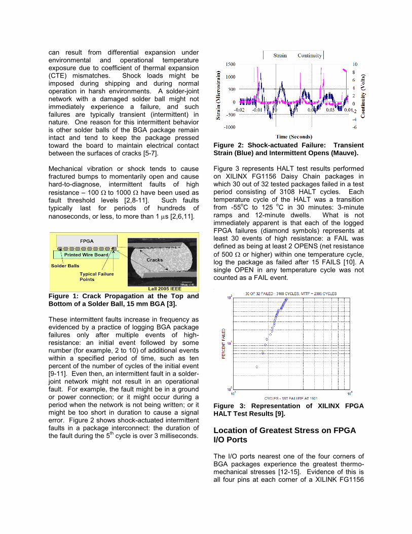
Figure 1: Crack Propagation at the Top and Bottom of a Solder Ball, 15 mm BGA [3]. These intermittent faults increase in frequency as evidenced by a practice of logging BGA package failures only after multiple events of high-resistance: an initial event followed by some number (for example, 2 to 10) of additional events within a specified period of time, such as ten percent of the number of cycles of the initial event [9-11]. Even then, an intermittent fault in a solder-joint network might not result in an operational fault. For example, the fault might be in a ground or power connection; or it might occur during a period when the network is not being written; or it might be too short in duration to cause a signal error. Figure 2 shows shock-actuated intermittent faults in a package interconnect: the duration of the fault during the 5th cycle is over 3 milliseconds.
Figure 2: Shock-actuated Failure: Transient Strain (Blue) and Intermittent Opens (Mauve). Figure 3 represents HALT test results performed on XILINX FG1156 Daisy Chain packages in which 30 out of 32 tested packages failed in a test period consisting of 3108 HALT cycles. Each temperature cycle of the HALT was a transition from -55oC to 125 oC in 30 minutes: 3-minute ramps and 12-minute dwells. What is not immediately apparent is that each of the logged FPGA failures (diamond symbols) represents at least 30 events of high resistance: a FAIL was defined as being at least 2 OPENS (net resistance of 500 or higher) within one temperature cycle, log the package as failed after 15 FAILS [10]. A single OPEN in any temperature cycle was not counted as a FAIL event.
Figure 3: Representation of XILINX FPGA HALT Test Results [9].
Location of Greatest Stress on FPGA I/O Ports
The I/O ports nearest one of the four corners of BGA packages experience the greatest thermo-mechanical stresses [12-15]. Evidence of this is all four pins at each corner of a XILINK FG1156
are ground connection pins. The next nearest I/O ports at each corner are strong candidates for testing by SJ BIST and monitoring by SJ Monitor because those I/O ports are likely to fail first.
State of the Art
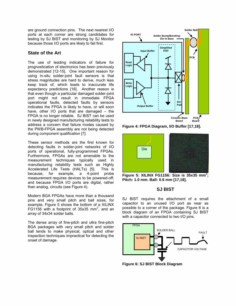
The use of leading indicators of failure for prognostication of electronics has been previously demonstrated [12-15]. One important reason for using in-situ solder-joint fault sensors is that stress magnitudes are hard to derive, much less keep track of, which leads to inaccurate life expectancy predictions [16]. Another reason is that even though a particular damaged solder-joint port might not result in immediate FPGA operational faults, detected faults by sensors indicates the FPGA is likely to have, or will soon have, other I/O ports that are damaged – the FPGA is no longer reliable. SJ BIST can be used in newly designed manufacturing reliability tests to address a concern that failure modes caused by the PWB-FPGA assembly are not being detected during component qualification [7]. These sensor methods are the first known for detecting faults in solder-joint networks of I/O ports of operational, fully-programmed FPGAs. Furthermore, FPGAs are not amenable to the measurement techniques typically used in manufacturing reliability tests such as Highly Accelerated Life Tests (HALTs) [5]. This is because, for example, a 4-point probe measurement requires devices to be powered-off; and because FPGA I/O ports are digital, rather than analog, circuits (see Figure 4). Modern BGA FPGAs have more than a thousand pins and very small pitch and ball sizes, for example, Figure 5 shows the bottom of a XILINX FG1156 with a footprint of 35x35 mm2, and an array of 34x34 solder balls. The dense array of fine-pitch and ultra fine-pitch BGA packages with very small pitch and solder ball tends to make physical, optical and other inspection techniques impractical for detecting the onset of damage.
Figure 4: FPGA Diagram, I/O Buffer [17,18].
Figure 5: XILINX FG1156: Size is 35x35 mm
2;
Pitch: 1.0 mm. Ball: 0.6 mm [17,18].
SJ BIST
SJ BIST requires the attachment of a small capacitor to an unused I/O port as near as possible to a corner of the package. Figure 6 is a block diagram of an FPGA containing SJ BIST with a capacitor connected to two I/O pins.
Figure 6: SJ BIST Block Diagram
FPGA
SJ BIST
SOLDER BALL
CAPACITOR VOLTAGE
FAULT
IO PORT
Read Logic
Simplified ESD
Solder Ball
PCB
Board
Output Buffer
Die Pad
Solder Bump/Bonding: Die to Base
PCB Land
Write Logic
Input Buffer
Ceramic Base
Board
Die
Referring to Figure 6, SJ BIST writes a logical ‘1’ to charge the capacitor and then reads the voltage across the charged capacitor. If the solder-joint network of the I/O port of the FPGA is undamaged, the write causes the capacitor to be fully charged and a logical ‘1’ is read by SJ BIST. When the solder-joint network is damaged, the effective resistance of the SJ network increases, the charging time constant increases, the write fails to sufficiently charge the capacitor, and a logical ‘0’ instead of a logical ‘1’ is read: a fault occurs, is detected by SJ BIST and is reported.
Test Results
SJ BIST was synthesized, programmed into test FPGAs and tested at various clock frequencies ranging from 10 KHz to 100 MHz and for varying solder-joint network conditions ranging from no fault to over 100 of fault resistance: All faults of 100 or larger were detected, and there were no false alarms.
Solder Joint No Fault and Fault Tests
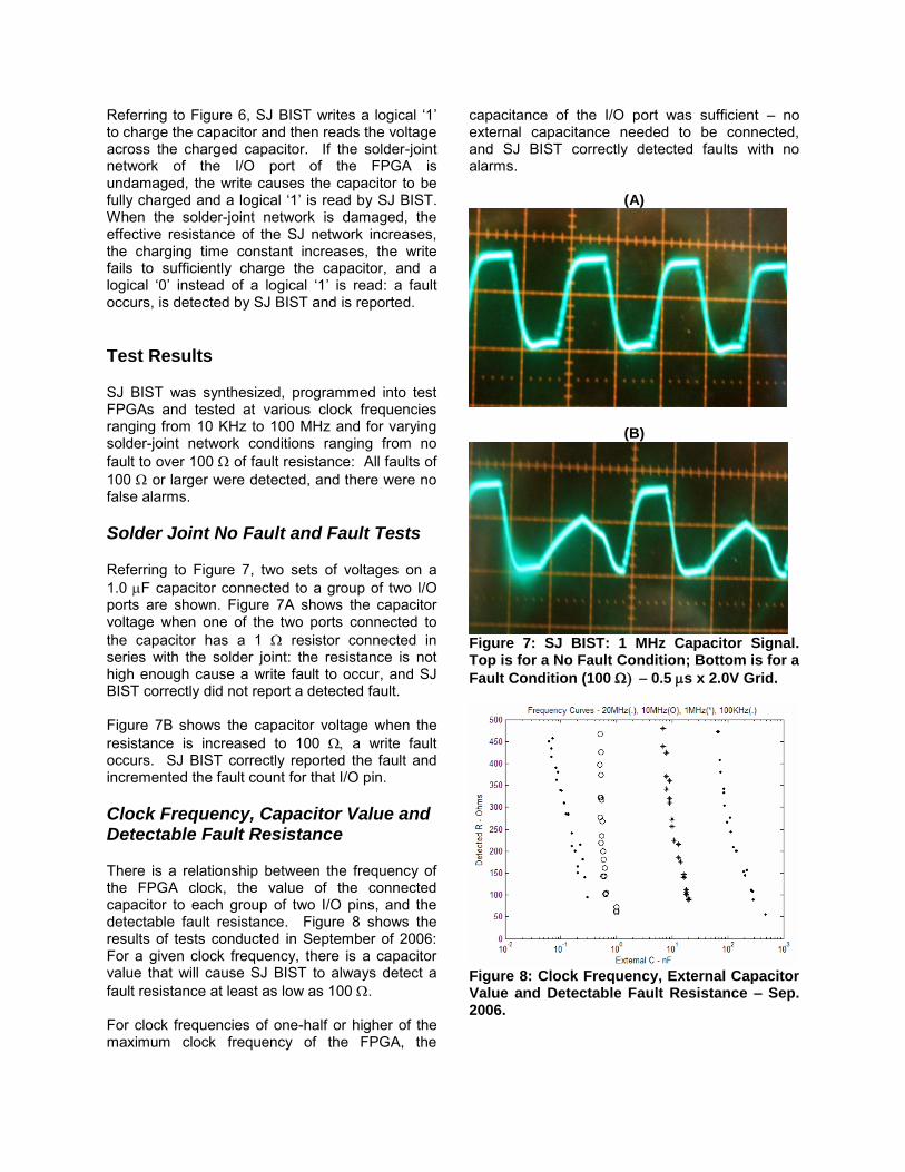
Referring to Figure 7, two sets of voltages on a 1.0 F capacitor connected to a group of two I/O ports are shown. Figure 7A shows the capacitor voltage when one of the two ports connected to the capacitor has a 1 resistor connected in series with the solder joint: the resistance is not high enough cause a write fault to occur, and SJ BIST correctly did not report a detected fault. Figure 7B shows the capacitor voltage when the resistance is increased to 100 a write fault occurs. SJ BIST correctly reported the fault and incremented the fault count for that I/O pin.
Clock Frequency, Capacitor Value and Detectable Fault Resistance
There is a relationship between the frequency of the FPGA clock, the value of the connected capacitor to each group of two I/O pins, and the detectable fault resistance. Figure 8 shows the results of tests conducted in September of 2006: For a given clock frequency, there is a capacitor value that will cause SJ BIST to always detect a fault resistance at least as low as 100 . For clock frequencies of one-half or higher of the maximum clock frequency of the FPGA, the
capacitance of the I/O port was sufficient – no external capacitance needed to be connected, and SJ BIST correctly detected faults with no alarms.
(A)
(B)
Figure 7: SJ BIST: 1 MHz Capacitor Signal. Top is for a No Fault Condition; Bottom is for a
Fault Condition (100 0.5 s x 2.0V Grid.
Figure 8: Clock Frequency, External Capacitor Value and Detectable Fault Resistance – Sep. 2006.
SJ BIST Sensitivity and Resolution
Given a correctly selected pair of CLK frequencies and capacitor values, SJ BIST is guaranteed to detect all faults at least as low as 100 (sensitivity) when the fault lasts at least two clock periods (resolution). For faults of shorter duration, the fault is detectable when it occurs shortly before the write and when it lasts about one-half of the clock period.
SJ BIST Signals
SJ BIST needs to present at least one error signal (a fault indicator) either to an external FPGA I/O port or to an internal fault management program. At least one control signal is required: an enable (disable) BIST.
Error Signals and Fault Counts
In addition to recording fault counts, the SJ BIST core has two error signals: (1) at least one fault has been detected in the 2-port network being tested and (2) at least one fault is currently active. A fault counter (1:255) is provided. For a deployed SJ BIST, we anticipate most applications would only use the two error signals. We also believe a deployed SJ BIST application would most likely use at least four groups of cores – one group of two I/O pins near each corner of an FPGA.
Control Signals
In addition to CLK, the SJ BIST core has two input signals: ENABLE and RESET. ENABLE is used to turn SJ BIST detection on and off; RESET is used to reset both the fault signal latches and the fault counters. For a deployed SJ BIST, RESET might not be used.
SJ MONITOR
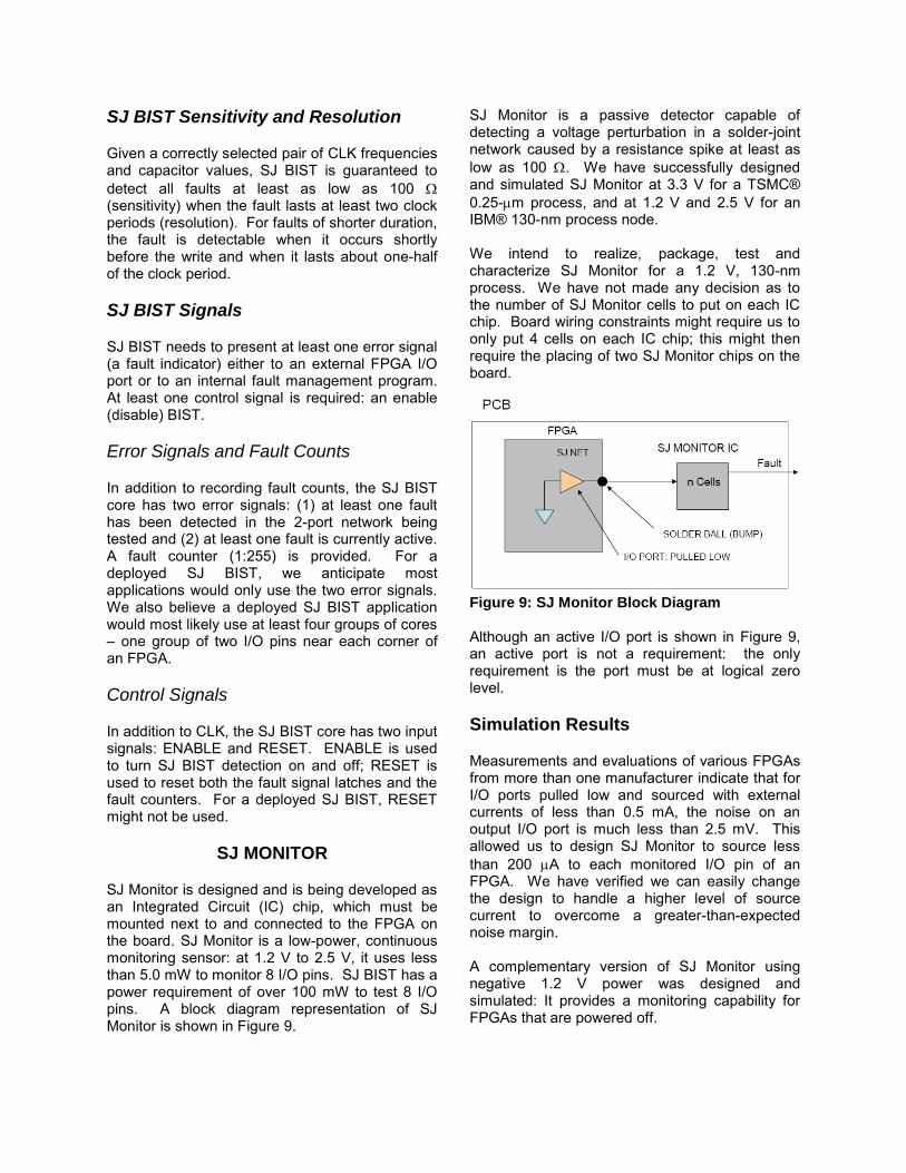
SJ Monitor is designed and is being developed as an Integrated Circuit (IC) chip, which must be mounted next to and connected to the FPGA on the board. SJ Monitor is a low-power, continuous monitoring sensor: at 1.2 V to 2.5 V, it uses less than 5.0 mW to monitor 8 I/O pins. SJ BIST has a power requirement of over 100 mW to test 8 I/O pins. A block diagram representation of SJ Monitor is shown in Figure 9.
SJ Monitor is a passive detector capable of detecting a voltage perturbation in a solder-joint network caused by a resistance spike at least as low as 100 . We have successfully designed and simulated SJ Monitor at 3.3 V for a TSMC® 0.25-m process, and at 1.2 V and 2.5 V for an IBM® 130-nm process node. We intend to realize, package, test and characterize SJ Monitor for a 1.2 V, 130-nm process. We have not made any decision as to the number of SJ Monitor cells to put on each IC chip. Board wiring constraints might require us to only put 4 cells on each IC chip; this might then require the placing of two SJ Monitor chips on the board.
Figure 9: SJ Monitor Block Diagram Although an active I/O port is shown in Figure 9, an active port is not a requirement: the only requirement is the port must be at logical zero level.
Simulation Results
Measurements and evaluations of various FPGAs from more than one manufacturer indicate that for I/O ports pulled low and sourced with external currents of less than 0.5 mA, the noise on an output I/O port is much less than 2.5 mV. This allowed us to design SJ Monitor to source less than 200 A to each monitored I/O pin of an FPGA. We have verified we can easily change the design to handle a higher level of source current to overcome a greater-than-expected noise margin. A complementary version of SJ Monitor using negative 1.2 V power was designed and simulated: It provides a monitoring capability for FPGAs that are powered off.
Noise Rejection and Fault Detection
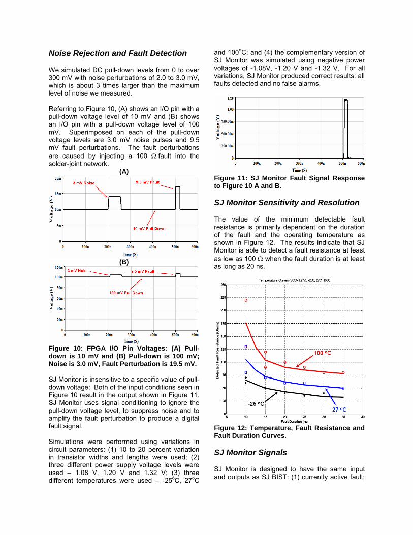
We simulated DC pull-down levels from 0 to over 300 mV with noise perturbations of 2.0 to 3.0 mV, which is about 3 times larger than the maximum level of noise we measured. Referring to Figure 10, (A) shows an I/O pin with a pull-down voltage level of 10 mV and (B) shows an I/O pin with a pull-down voltage level of 100 mV. Superimposed on each of the pull-down voltage levels are 3.0 mV noise pulses and 9.5 mV fault perturbations. The fault perturbations are caused by injecting a 100 fault into the solder-joint network.
(A)
(B)
Figure 10: FPGA I/O Pin Voltages: (A) Pull-down is 10 mV and (B) Pull-down is 100 mV; Noise is 3.0 mV, Fault Perturbation is 19.5 mV. SJ Monitor is insensitive to a specific value of pull-down voltage: Both of the input conditions seen in Figure 10 result in the output shown in Figure 11. SJ Monitor uses signal conditioning to ignore the pull-down voltage level, to suppress noise and to amplify the fault perturbation to produce a digital fault signal. Simulations were performed using variations in circuit parameters: (1) 10 to 20 percent variation in transistor widths and lengths were used; (2) three different power supply voltage levels were used – 1.08 V, 1.20 V and 1.32 V; (3) three different temperatures were used – -25oC, 27oC
and 100oC; and (4) the complementary version of SJ Monitor was simulated using negative power voltages of -1.08V, -1.20 V and -1.32 V. For all variations, SJ Monitor produced correct results: all faults detected and no false alarms.
Figure 11: SJ Monitor Fault Signal Response to Figure 10 A and B.
SJ Monitor Sensitivity and Resolution
The value of the minimum detectable fault resistance is primarily dependent on the duration of the fault and the operating temperature as shown in Figure 12. The results indicate that SJ Monitor is able to detect a fault resistance at least as low as 100 when the fault duration is at least as long as 20 ns.
Figure 12: Temperature, Fault Resistance and Fault Duration Curves.
SJ Monitor Signals
SJ Monitor is designed to have the same input and outputs as SJ BIST: (1) currently active fault;

(2) at least one fault detected since last reset; (3) enable input; (4) reset input; (5) count of the number of faults detected (1:255).
SJ Monitor Power
Test simulations showed SJ Monitor has a power requirement of between 0.9 mW and 2.4 mW to monitor 8 I/O pins, depending on temperature and voltage. This low power requirement makes SJ Monitor suitable for continuous monitoring and for short test applications.
Figure 13: Power Used vs Temperature and Supply Voltage (VCC).
INTERMITTENCY MITIGATION
SJ BIST and SJ Monitor are very useful sensors for mitigating intermittencies when corner I/O pins of a BGA package are monitored. Early detection of failure of an unused I/O pin allows the electronic board to be replaced before subsequent fatigue damage causes an application I/O pin to fail, and therefore intermittent operational anomalies are avoided. Reported detection of one or more faults can be used to confirm that the electronic board with that FPGA is a likely candidate for replacement to address reported opearational anomalies.
PRESENT ACTIVITIES
Extensive experiments, including HALTs, have been planned and are presently being conducted.
The primary objectives are the following: (1) perform final sensitivity, resolution and clock frequency measurements to update Figure 8; (2) collect, evaluate and publish statistical data related to test I/O port location, first failure and probability of failure distribution. Figure 14 is a footprint for a XILINX FG1156 FPGA showing the I/O pins (shaded) we selected for testing by SJ BIST. Sixty-four I/O pins were selected, so there are 32 groups of SJ BIST cores in our test program.
Figure 14: FG1156 Footprint Showing Selected SJ BIST I/O Pins: 32 Groups, 64 Pins. Figure 15 is a block diagram of the HALT test board we designed. We load the SJ BIST test program into a PROM, which then loads the program into each FPGA when the board is powered on. Each FPGA generates 640 bits of data (64 x (2 faults signals + 8 bits of count)); each board generates 2560 bits of data, and we have 4 boards in the HALT oven = 10,240 bits of data for each sample period. We wrote a LabVIEW® program to control the collection of data, and we wrote a MATLAB® program to process the data. Figure 16 shows a manufactured, populated and soldered HALT test board. There are three connectors: (1) XILINX programmer connection, (2) power input and (3) experiment control connections.
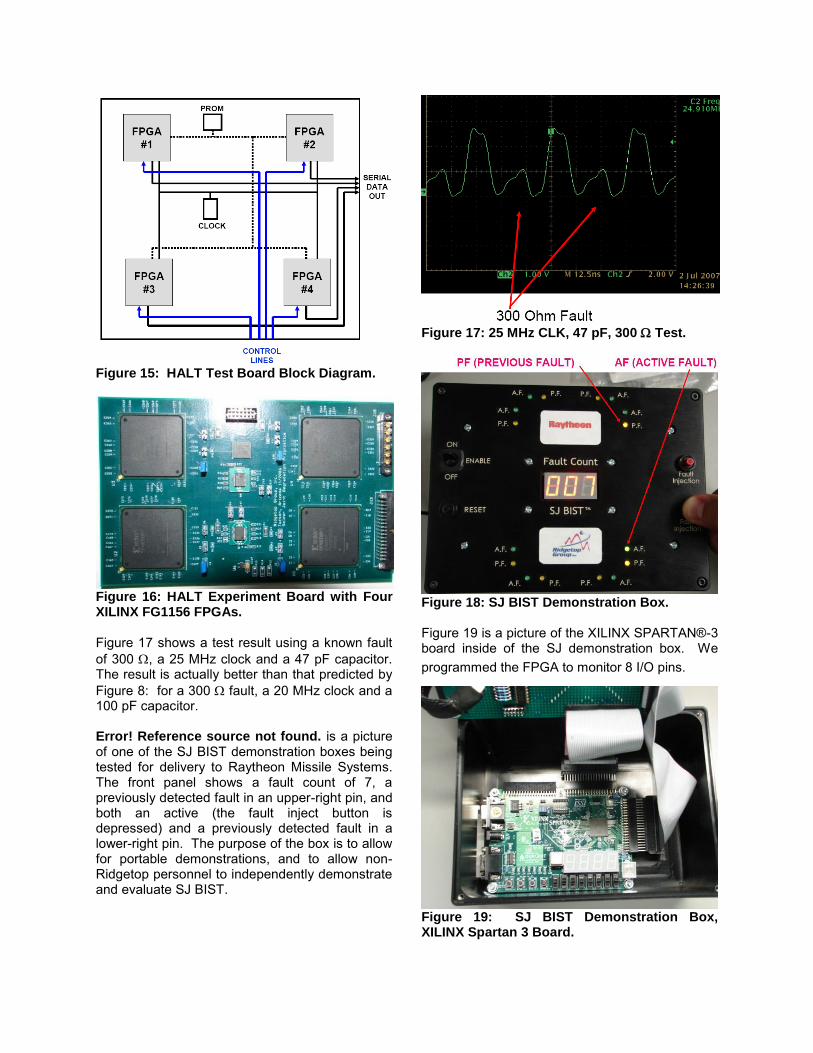
Figure 15: HALT Test Board Block Diagram.
Figure 16: HALT Experiment Board with Four XILINX FG1156 FPGAs. Figure 17 shows a test result using a known fault of 300 , a 25 MHz clock and a 47 pF capacitor. The result is actually better than that predicted by Figure 8: for a 300 fault, a 20 MHz clock and a 100 pF capacitor. Error! Reference source not found. is a picture of one of the SJ BIST demonstration boxes being tested for delivery to Raytheon Missile Systems. The front panel shows a fault count of 7, a previously detected fault in an upper-right pin, and both an active (the fault inject button is depressed) and a previously detected fault in a lower-right pin. The purpose of the box is to allow for portable demonstrations, and to allow non-Ridgetop personnel to independently demonstrate and evaluate SJ BIST.
Figure 17: 25 MHz CLK, 47 pF, 300 Test.
Figure 18: SJ BIST Demonstration Box. Figure 19 is a picture of the XILINX SPARTAN®-3 board inside of the SJ demonstration box. We programmed the FPGA to monitor 8 I/O pins.
Figure 19: SJ BIST Demonstration Box, XILINX Spartan 3 Board.

Figure 20 is a picture of the display control board for the SJ BIST demonstration board. The board provides the interface and control between the box front panel and the FPGA. Not shown is a small board upon which the 7-segment LED is mounted. Future versions of the SJ BIST demonstration box will use a printed circuit board instead of a bread board.
Figure 20: SJ BIST Demonstration Box, Display Board.
SUMMARY
In this paper we provided updated information on SJ BIST, which was originally presented in 2006, and we introduced a new solder-joint fault sensor, SJ Monitor. A brief overview of the mechanics-of-failure was included: the primary contributor to fatigue damage is thermo-mechanical stresses related to CTE mismatches, shock and vibration, and power on-off sequencing. Solder-joint fatigue damage can result in fractures that cause intermittent instances of high-resistance spikes that are hard-to-diagnose. In reliability testing, OPENS (faults) are often characterized by spikes of a 100 or more lasting for less than 100 ns to 1 s or longer. Prior to SJ BIST and SJ Monitor, there were no known methods for detecting high-resistance faults in solder-joint networks belonging to the I/O ports of operational, fully-programmed FPGAs. An in-situ SJ BIST or SJ Monitor to test or monitor selected I/O pins is useful because stress magnitudes are hard to derive, which leads to inaccurate life expectancy predictions; and even though a particular damaged solder-joint port might not result in immediate FPGA operational failure, the damage indicates the FPGA is no
longer reliable. SJ BIST can also be used in newly designed manufacturing reliability tests to investigate failure modes related to the PWB-FPGA assembly.
ACKNOWLEDGMENT
The work presented in this paper was funded by Small Business Innovation Research contract awards from the Department of Defense, Naval Air, Joint Strike Fighter program: Contract No. N68335-06-C-0356 P00002. Final patent applications have been filed: one for SJ BIST technology and one for SJ Monitor technology. U.S. Patent 7,196,294, Mar. 27, 2007, has been issued for a related technology.
REFERENCES
[1]. J.P. Hofmeister, P. Lall and Russ Graves, “In-Situ, Real-Time Detector for Faults in Solder Joints Belonging to Operational, Fully Programmed FPGAs,” Proceedings, IEEE AUTOTESTCON 2006, Anaheim, CA, Sep. 18-21, 2006, pp-237-243.
[2]. Accelerated Reliability Task IPC-SM-785, SMT Force Group Standard, Product Reliability Committee of the IPC, Published by Analysis Tech., Inc., 2005, www.analysistech.com/event-tech-IPC-SM-785.
[3]. P. Lall, M.N. Islam, N. Singh, J.C. Suhling and R. Darveaux, “Model for BGA and CSP Reliability in Automotive Underhood Applications,” IEEE Trans. Comp. and Pack. Tech.,Vol. 27, No. 3, Sep. 2004, pp. 585-593.
[4]. R. Gannamani, V. Valluri, Sidharth and M-L Zhang, “Reliability evaluation of chip scale packages,” Advanced Micro Devices, Sunnyvale, CA, in Daisy Chain Samples, Application Note, Spansion, July 2003, pp. 4-9.
[5]. Sony Semiconductor Quality and Reliability Handbook, Revised May 2001, http://www.sony.net/products/SC-HP/tec/catalog, Vol. 2, pp. 66-67, Vol. 4, pp. 120-129.
[6]. Use Condition Based Reliability Evaluation: An Example Applied to Ball Grid Array (BGA) Packages, SEMATECH Technology Transfer #99083813A-XFR, International SEMATECH, 1999, pg. 6.
[7]. Comparison of Ball Grid Array (BGA) Component and Assembly Level Qualification Tests and Failure Modes, SEMATECH
Technology Transfer #00053957A-XFR, International SEMATECH, May 31, 2000, pp. 1-4.
[8]. R. Roergren, P-E. Teghall and P. Carlsson, “Reliability of BGA Packages in an Automotive Environment,” IVF-The Swedish Institute of Production Engineering Research, Argongatan 30, SE-431 53 Moelndal, Sweden, http://www.ivf.se, accessed Dec. 25, 2005.
[9]. D.E. Hodges Popp, A. Mawer and G. Presas, “Flip chip PBGA solder joint reliability: power cycling versus thermal cycling,” Motorola Semiconductor Products Sector, Austin, TX, Dec. 19, 2005.
[10]. The Reliability Report, XILINX, xgoogle.xilinx.com, Sep. 1, 2003, pp. 225-229.
[11]. J-P. Clech, D.M. Noctor, J.C. Manock, G.W. Lynott and F.E. Bader, “Surface mount assembly failure statistics and failure-free times,” in Proceedings, 44
th ECTC, Washington, D.C., May
1-4, 1994, pp. 487-497.
[12]. P. Lall, P. Choudhary and S. Gupte, “Health Monitoring for Damage Initiation & Progression during Mechanical Shock in Electronic Assemblies,” Proceedings of the 56
th IEEE
Electronic Components and Technology Conference, San Diego, California, pp. 85-94, May 30-June 2, 2006.
[13]. P. Lall, M. Hande, M.N. Singh, J. Suhling and J. Lee, “Feature Extraction and Damage Data for Prognostication of Leaded and Leadfree Electronics,” Proceedings of the 56
th IEEE
Electronic Components and Technology Conference, San Diego, California, pp.718-727, May 30-June 2, 2006.
[14]. P. Lall, N. Islam and J. Suhling, “Leading Indicators of Failure for Prognostication of Leaded and Lead-Free Electronics in Harsh Environments,” Proceedings of the ASME InterPACK Conference, San Francisco, CA, Paper IPACK2005-73426, pp. 1-9, July 17-22, 2005.
[15]. P. Lall, M.N. Islam, K. Rahim and J. Suhling, “Prognostics and Health Management of Electronic Packaging,” Accepted for Publication in IEEE Transactions on Components and Packaging Technologies, Paper Available in Digital Format on IEEE Explore, pp. 1-12, March 2005.
[16]. P. Lall, “Challenges in Accelerated Life Testing,” Inter Society Conf., Thermal Phenomena, 2004, pg. 727.
[17]. XILINX Fine-Pitch BGA (FG1156/FGG1156) Package, PK039 (v1.2), June 25, 2004.
[18]. R.R Tummala, EJ. Rymaszewski and A.G. Klopfenstein, Ed., Microelectronics Packaging Handbook, Semiconductor Packaging Part II, Kluwer Academic Publishers, 2nd Ed., 1999, pp. II-62 to II-185.
IBM is a registered trade mark of IBM Corp. LabVIEW is a registered trade mark of National Instruments MATLAB is a registered trade mark of Mathworks, Inc. SPARTAN is a registered trade mark of Xilinx, Inc. TSMC is a registered trade mark of Taiwan Semiconductor Manufacturing Corporation. XILINX is a registered trade mark of Xilinx, Inc.