introduction to fpgas dr. philip brisk department of computer science and engineering university of...
TRANSCRIPT
Introduction to FPGAs
Dr. Philip BriskDepartment of Computer Science and Engineering
University of California, Riverside
CS 223

The Basics
SRAM
Transistor
1
Open Closed
0

Configuration Comes at a Cost
4-6 T
1T
SRAM
+ Configuration circuitry+ Error detection/correction+ Security features
6T SRAM
4T SRAM
https://en.wikipedia.org/wiki/Static_random-access_memory

Lookup Tables (LUTs)
SRAM
SRAM
SRAM
SRAM
x y Commercial FPGAs• Xilinx: 6-LUT• Altera: 6-LUT• Microsemi: 4-LUT
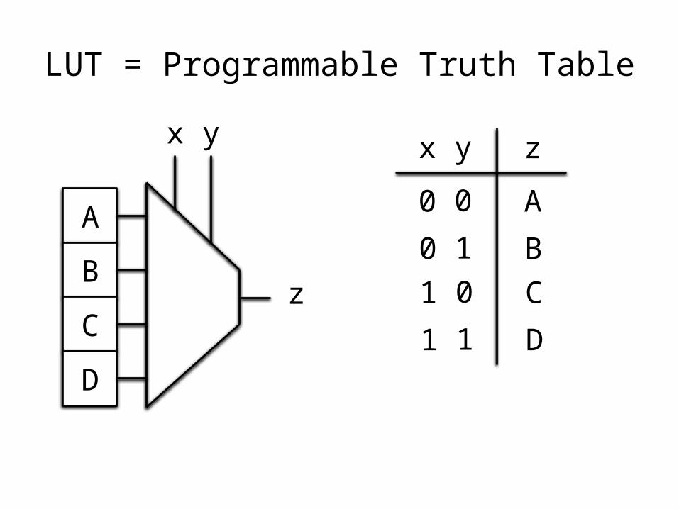
LUT = Programmable Truth Table
A
B
C
D
x y zx y
z
0 0 A
0 1 B1 0 C
1 1 D
AND
0
0
0
1
x y zx y
z
0 0 0
0 1 01 0 0
1 1 1

OR
0
1
1
1
x y zx y
z
0 0 0
0 1 11 0 1
1 1 1

NAND
1
1
1
0
x y zx y
z
0 0 1
0 1 11 0 1
1 1 0
NOR
1
0
0
0
x y zx y
z
0 0 1
0 1 01 0 0
1 1 0
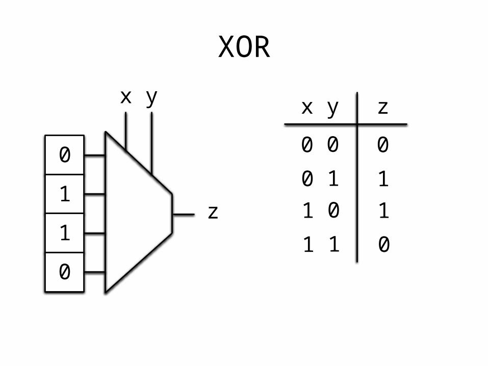
XOR
0
1
1
0
x y zx y
z
0 0 0
0 1 11 0 1
1 1 0
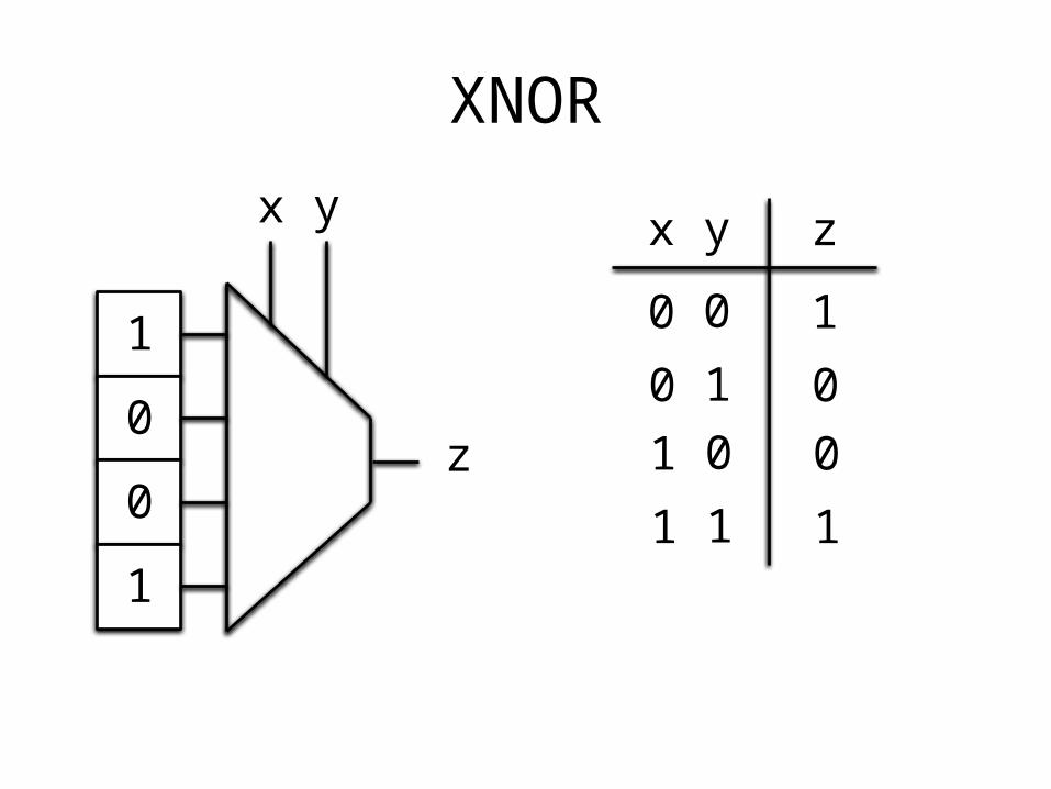
XNOR
1
0
0
1
x y zx y
z
0 0 1
0 1 01 0 0
1 1 1
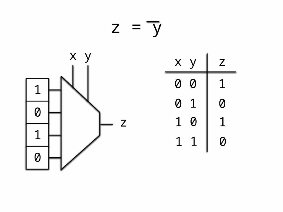
z = y
1
0
1
0
x y zx y
z
0 0 1
0 1 01 0 1
1 1 0

z = y + x
1
0
1
1
x y zx y
z
0 0 1
0 1 01 0 1
1 1 1
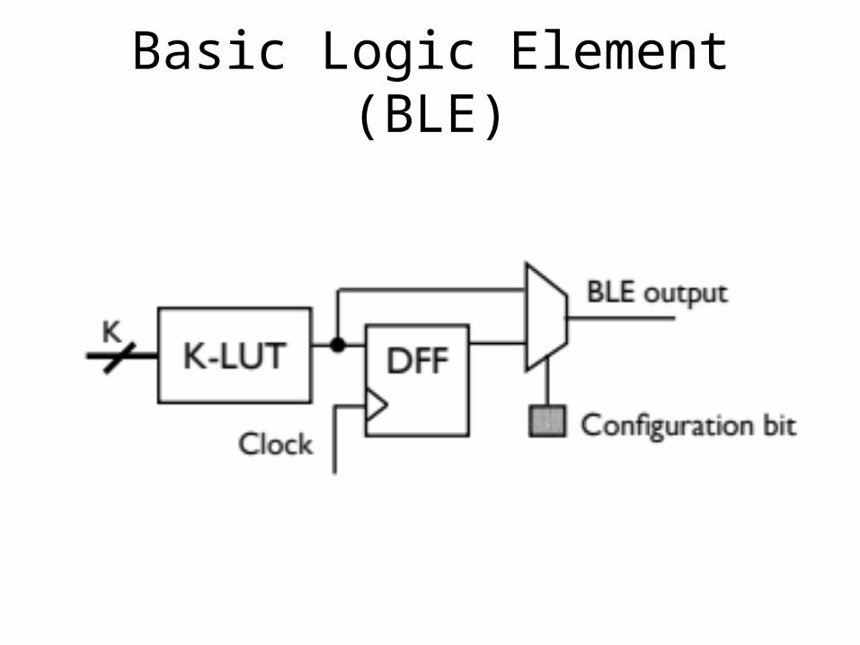
Basic Logic Element (BLE)
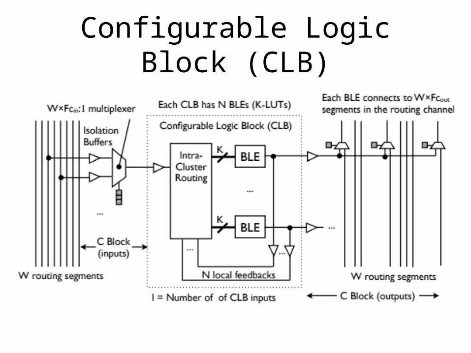
Configurable Logic Block (CLB)
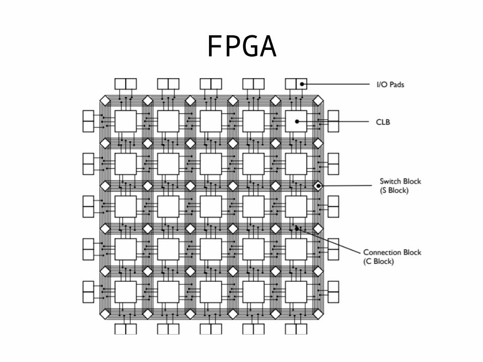
FPGA
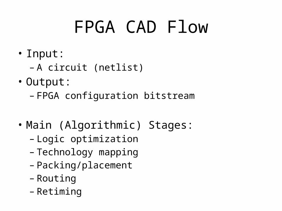
FPGA CAD Flow• Input: – A circuit (netlist)
• Output: – FPGA configuration bitstream
• Main (Algorithmic) Stages: – Logic optimization– Technology mapping– Packing/placement– Routing– Retiming

Technology Mapping
Ling et al., DAC 2005, Fig. 2
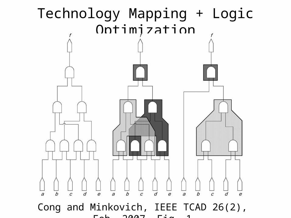
Technology Mapping + Logic Optimization
Cong and Minkovich, IEEE TCAD 26(2), Feb. 2007, Fig. 1
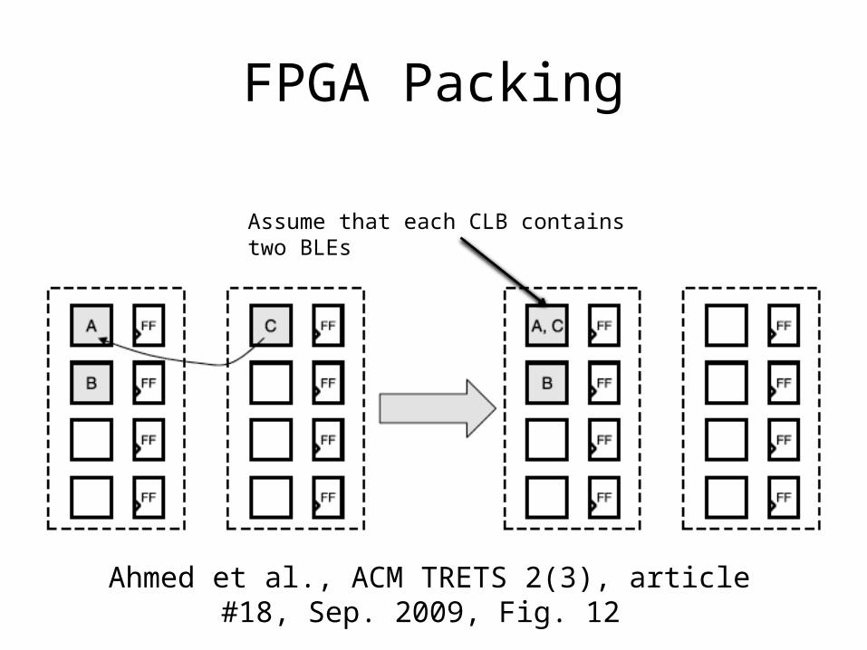
FPGA Packing
Ahmed et al., ACM TRETS 2(3), article #18, Sep. 2009, Fig. 12
Assume that each CLB contains two BLEs
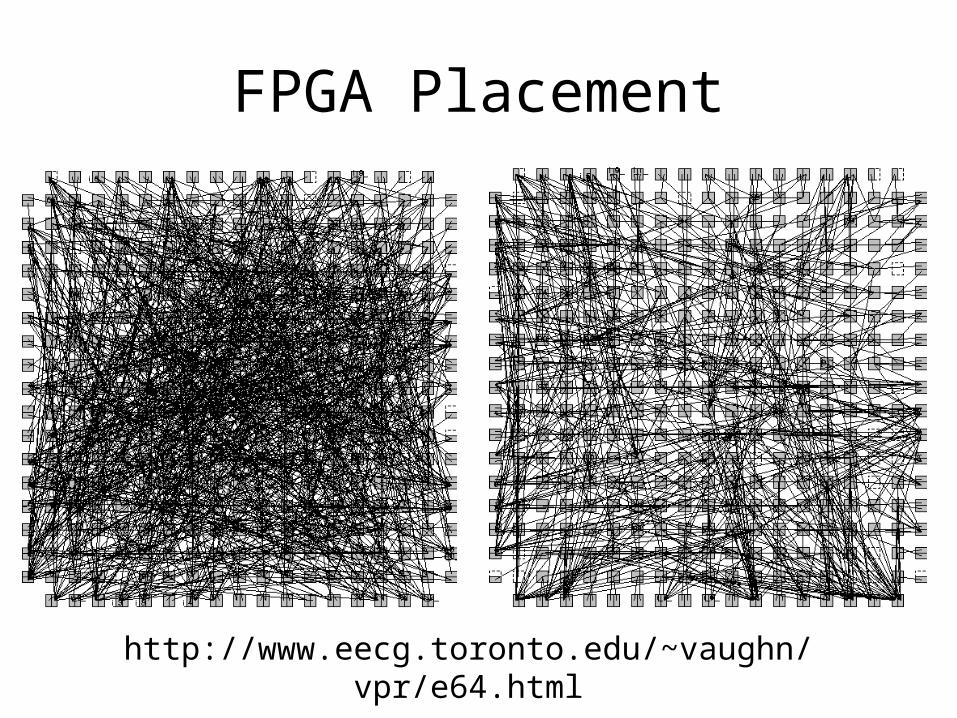
FPGA Placement
http://www.eecg.toronto.edu/~vaughn/vpr/e64.html

FPGA Routing
http://www.eecg.toronto.edu/~vaughn/vpr/e64.html
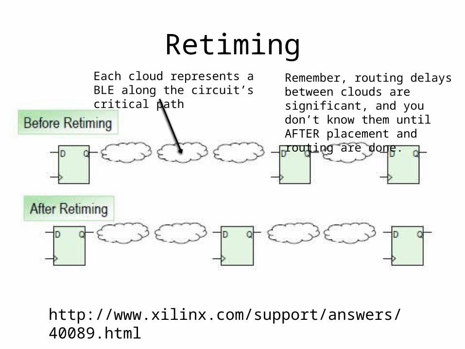
Retiming
http://www.xilinx.com/support/answers/40089.html
Each cloud represents a BLE along the circuit’s critical path
Remember, routing delays between clouds are significant, and you don’t know them until AFTER placement and routing are done.

Introduction to FPGA Design
J. Serrano, CERN, Geneva, Switzerlandhttp://cds.cern.ch/record/1100537/files/p231.pdf
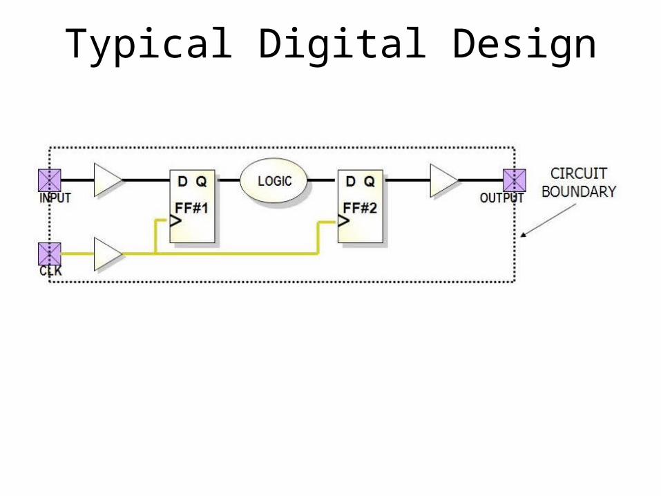
Typical Digital Design
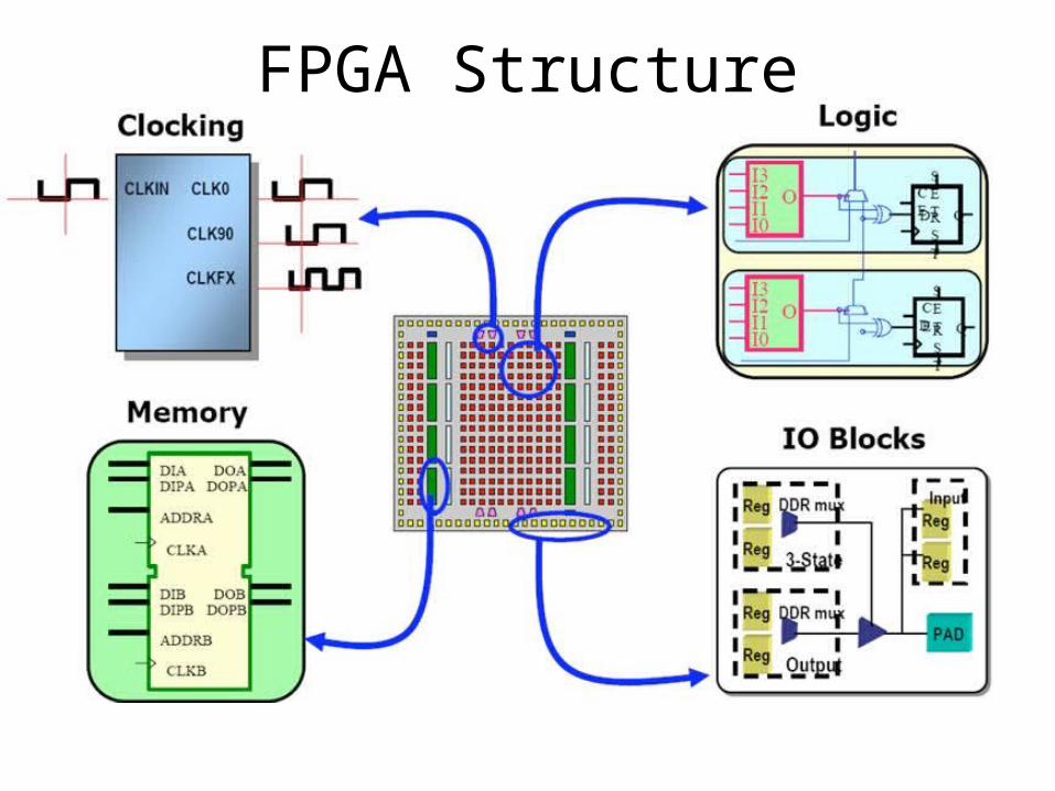
FPGA Structure

Signal Processing: CPU vs. FPGA
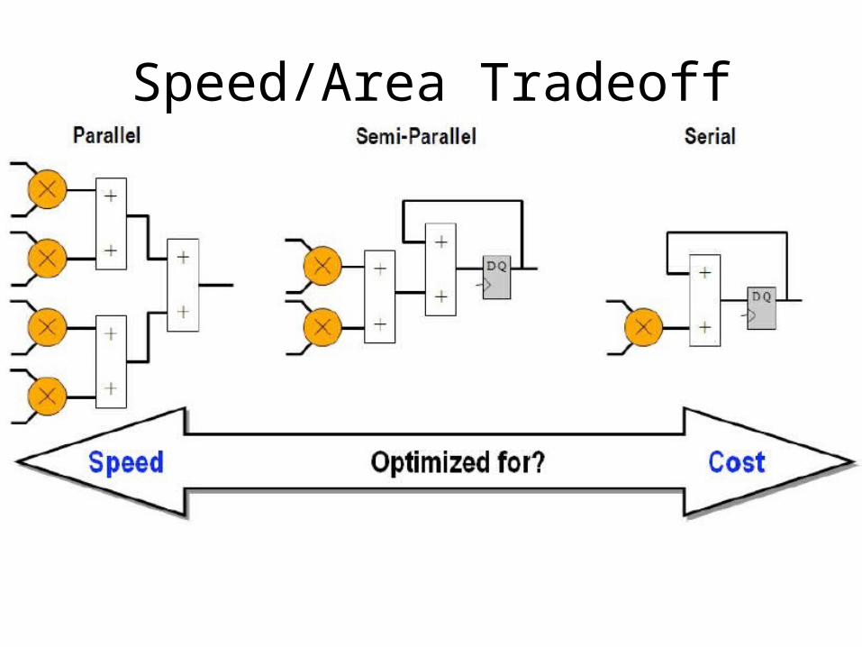
Speed/Area Tradeoff
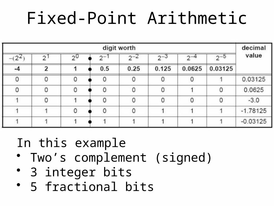
Fixed-Point Arithmetic
In this example• Two’s complement (signed)• 3 integer bits• 5 fractional bits

Truncation vs. Rounding in Fixed-Point
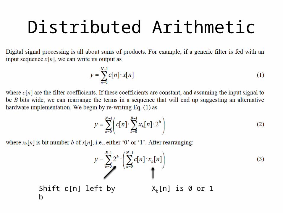
Distributed Arithmetic
Xb[n] is 0 or 1Shift c[n] left by b
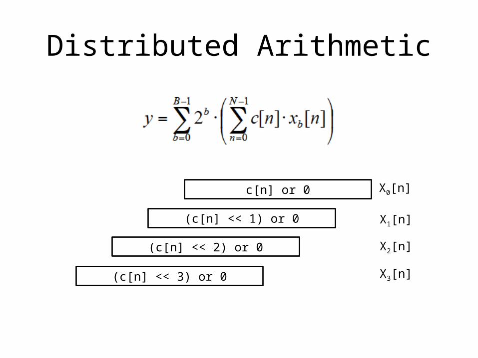
c[n] or 0
(c[n] << 1) or 0
(c[n] << 2) or 0
(c[n] << 3) or 0
X0[n]
X1[n]
X2[n]
X3[n]
Distributed Arithmetic

Distributed Arithmetic Architecture
Course Topics
• FPGA architectures– Academic (VPR)– Commercial (Xilinx / Altera / Microsemi)
• FPGA CAD algorithms• Compilers (e.g., C, OpenCL, etc. to FPGA)• FPGA Applications• Reconfigurable alternatives to FPGAs• The history of reconfigurable computing– Going back to the vacuum tube era