introduction to op ti system and practical optical systems
TRANSCRIPT

Introduction to Optisystem
And practical optical systems
Simulations and design by

Introduction to Optisystem :
Optisystem is a professional modern simulation software
produced by Optiwave Company which made great efforts in the
interests of optical communications system and practical
applications of optical networks, Fig. 4-1 shows Optiwave and
Optisystem logos.
Fig. 4-1, Optiwave and Optisystem logos
What kinds of Applications can be done?
OptiSystem gives us the ability to simulate/design:
• Next Generation optical networks.
• Current optical networks.
• SONET/SDH ring networks.
• Amplifiers, receivers, transmitters.
What about Analysis Tools provided?
OptiSystem enables users to simulate and get results via great
tools provided such as:
• Eye diagrams, BER, Q-Factor, and Signal chirp.
• Polarization state, Constellation diagrams.
• Signal power, gain, noise figure, OSNR.
• Data monitors, report generation, and more!

Getting Started with Optisystem Environment :
After Optisystem being installed, we can do all benefits of
simulations and designs, let's start here!
• To start the program go:
Start menu� Programs� Optiwave Software� Optisystem 7�
Optisystem, as shown in Fig. 4-2.
Fig. 4-2, Path toward Optisystem
When Optisystem opens, the main window would be as shown
in Fig. 4-3.
Fig. 4-3, main window of Optisystem
Basic optical components and systems:
Simulations and designs in Optisystem in mainly depends on
block diagrams, we place all needed blocks of sources,
channels, multiplexers, scopes…etc then run the simulation to
get results.
Example 4-1: simple optical transmitter system:
Create a new design work sheet and place the following
components from the default library directory to the left of the
workspace.
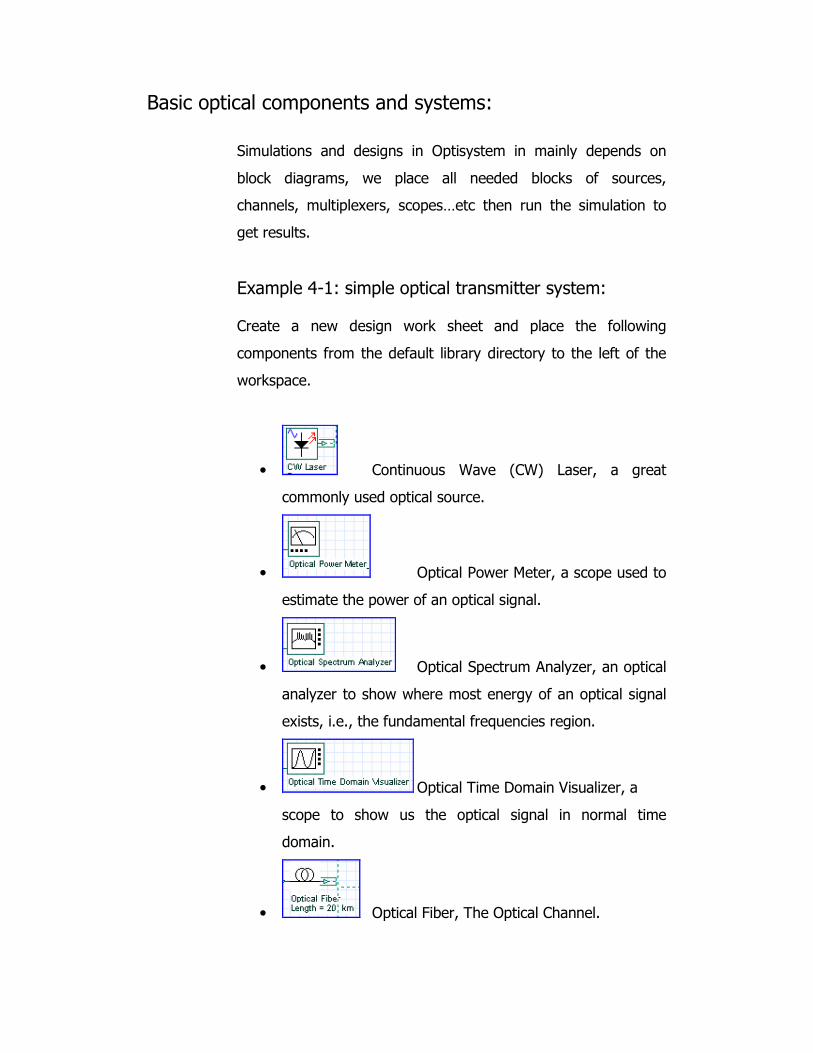
• Continuous Wave (CW) Laser, a great
commonly used optical source.
• Optical Power Meter, a scope used to
estimate the power of an optical signal.
• Optical Spectrum Analyzer, an optical
analyzer to show where most energy of an optical signal
exists, i.e., the fundamental frequencies region.
• Optical Time Domain Visualizer, a
scope to show us the optical signal in normal time
domain.
• Optical Fiber, The Optical Channel.
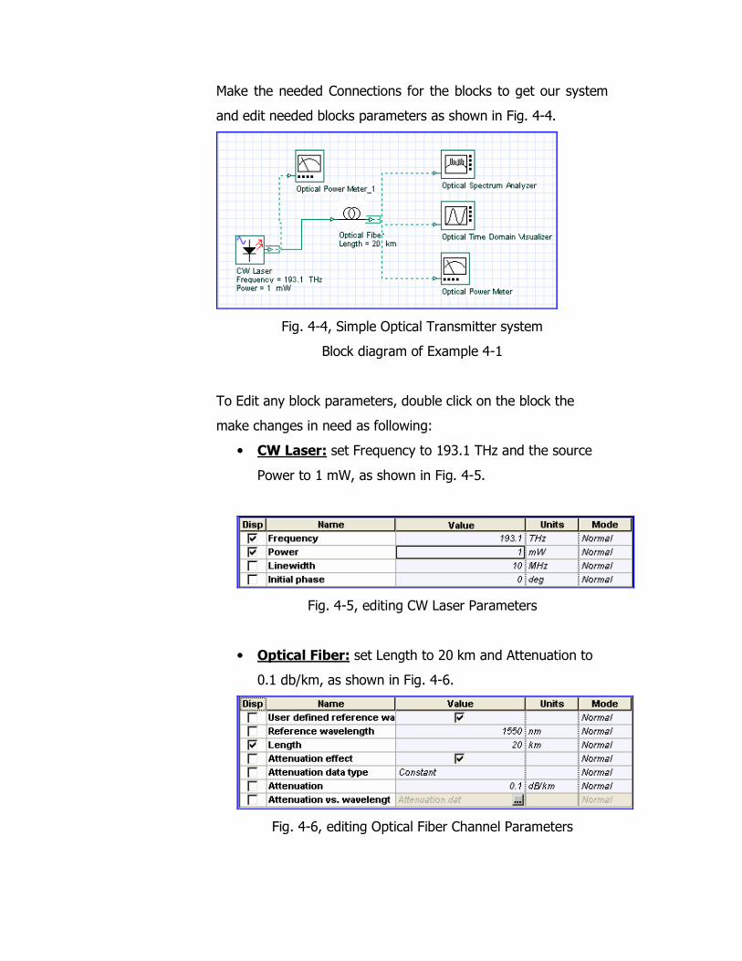
Make the needed Connections for the blocks to get our system
and edit needed blocks parameters as shown in Fig. 4-4.
Fig. 4-4, Simple Optical Transmitter system
Block diagram of Example 4-1
To Edit any block parameters, double click on the block the
make changes in need as following:
• CW Laser: set Frequency to 193.1 THz and the source
Power to 1 mW, as shown in Fig. 4-5.
Fig. 4-5, editing CW Laser Parameters
• Optical Fiber: set Length to 20 km and Attenuation to
0.1 db/km, as shown in Fig. 4-6.
Fig. 4-6, editing Optical Fiber Channel Parameters
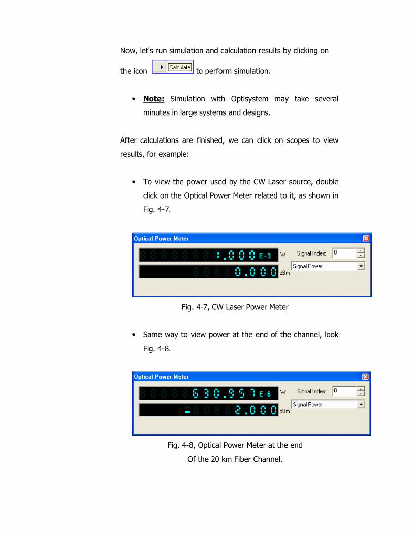
Now, let's run simulation and calculation results by clicking on
the icon to perform simulation.
• Note: Simulation with Optisystem may take several
minutes in large systems and designs.
After calculations are finished, we can click on scopes to view
results, for example:
• To view the power used by the CW Laser source, double
click on the Optical Power Meter related to it, as shown in
Fig. 4-7.
Fig. 4-7, CW Laser Power Meter
• Same way to view power at the end of the channel, look
Fig. 4-8.
Fig. 4-8, Optical Power Meter at the end
Of the 20 km Fiber Channel.

• Now let's see the Optical Spectrum Analyzer to
investigate fundamental frequency of transmitted signal,
look Fig. 4-9.
Fig. 4-9, Spectrum Analyzer Scope Screen
� Notes:
• Spectrum Analyzer results are shown versus the
Wavelength which more commonly used instead of
Frequency in Optical Communications.
• It's known that Wavelength of Light is related to
Frequency as following:
f
c=λ where,
λ: wavelength
c: speed of light ≈ 300000 km/s. f: frequency.
Thus in our case we have:
553.1101.193
103
12
8
≈×
×≈=
f
cλ µM

Example 4-2: 16-QAM Modulation system:
Create a new design work sheet and build in the following
system shown in Fig. 4-10 by placing components directly from
the library directory to the left of the workspace.
Fig. 4-10, Design for Example 4-2
New blocks used are:
• Pseudo-Random Bit Sequence
Generator, Used to generate bits sequence randomly.
• QAM Pulse Generator, Used to
generate M-Array QAM Pluses/Symbols.

• Electrical Constellation
Visualizer, a scope to scatter-plot the symbols in
Constellation diagram.
• Electrical Adder, used to perform the
summation of 2 electrical signals.
• Electrical Phase Shift, used to
delay/shift the phase of an electrical signal.
• Noise Source, simulates the noise at
specific noise power.
• Mach-Zehnder Modulator, to
modulate the optical signal according to the electrical
pulses.
To Edit any block parameters, double click on the block the
make changes in need as following:
• QAM Pulse Generator: set the bits per symbol to 4 to
get a 16-QAM system and the duty cycle to 1(100%) as
shown in Fig. 4-11.
Fig. 4-11, Parameters for QAM Pulse Generator

• Electrical Phase Shift: set the Phase shift to 90 deg,
which will be used to prepare the imaginary part of the
QAM scheme, look Fig. 4-12.
Fig. 4-12, Parameters for Electrical Phase Shift
• Noise Source: set the Noise Power to be -80 dBm as
shown in Fig. 4-13.
Fig. 4-13, Parameters for the Noise Source
Now, let's run simulation and calculation results by clicking on
the icon to perform simulation.
After calculations are finished, we can click on scopes to view
results, for example:
• To view the Constellation of the 16-QAM, double click on
the Electrical Constellation Visualizer, look Fig. 4-14.
Fig. 4-14, Constellation of 16-QAM

• To view the optical signal transmitted after modulation,
double click on the Time Domain Optical Visualizer, look
Fig. 4-15.
Fig. 4-15, Time Domain Optical signal
Notice the noise effect!
� Notes:
• Optisystem provides abilities to design many other
common modulation systems such as PSK, PAM,
FSK and son on using same methods.
• By applying the number of bits needed for each
symbol we then apply the system to be Binary, 4,
8, 16, 64, 128…-QAM.
• It's a good practice to set noise power to practical
values, thus our design be more realistic.

Example 4-3: WDM Optical System with 4 Channels:
Create a new design work sheet and build in the following
system shown in Fig. 4-16(a, b and c) by placing components
directly from the library directory to the left of the workspace.
Note: The Design is wide to show in a single Fig. so we have
portioned it into 3 graphs as shown in Fig. 4-16(a, b and c).
Fig. 4-16-a, Design of Example 4-3,
These blocks are the most left
in the Design work sheet

Fig. 4-16-b, Design of Example 4-3,
These blocks are the middle
in the Design work sheet
Fig. 4-16-c, Design of Example 4-3,
These blocks are the most right
in the Design work sheet
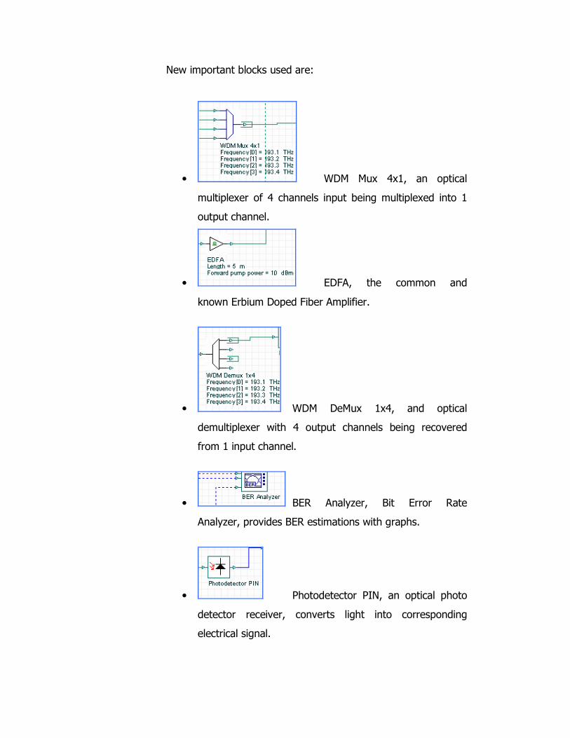
New important blocks used are:
• WDM Mux 4x1, an optical
multiplexer of 4 channels input being multiplexed into 1
output channel.
• EDFA, the common and
known Erbium Doped Fiber Amplifier.
• WDM DeMux 1x4, and optical
demultiplexer with 4 output channels being recovered
from 1 input channel.
• BER Analyzer, Bit Error Rate
Analyzer, provides BER estimations with graphs.
• Photodetector PIN, an optical photo
detector receiver, converts light into corresponding
electrical signal.

• Low Pass Gaussian Filter, a
low pass electrical filter with Gaussian response.
• RZ Pulse Generator, a return to zero
pulses generator from bits sequence.
• WDM Analyzer, a tool helps in
WDM analyzing.
Now, let's run simulation and calculation results by clicking on
the icon to perform simulation. Then we can click on scopes to view results, for example:
• To view the optical spectrum of the multiplexed
channels, double click on the optical spectrum, look
Fig. 4-17 below.
Fig. 4-17, Optical spectrum of the 4 multiplexed channels

• The WDM Analyzer can give us some useful
information about the multiplexed channels and how
much each channel is affected by noise, see Fig. 4-18.
Fig. 4-18, WDM Analyzer Window
• The other important estimation is the BER information
so make double click on the BER Analyzer block and
mark the Shoe Eye Diagram, Fig. 4-19.
Fig. 4-19, Details about BER and Eye Diagram
The Analyzer as well shows the Eye Diagram as shown in
Fig. 4-20 below.
Fig. 4-20, Eye Diagram shown by BER Analyzer