investigation of superlattice - nasa
TRANSCRIPT

NASA Contractor Report 3903 [ NASA-CR-390319850020840
Investigation of SuperlatticeDevice Structures
Isoris S. Gergis, Harold M. Manasevit,Alice L. Lin, and A. Brooke Jones
CONTRACT NAS1-16102
JUNE 1985
..,,,, .[,
[.:d_.S,!..S; r? :r v F (h-!_ [E,r.,:LI-::(- !;".',??_::A
_-_\'_:!: ',: !' L . !.I()D'.!A
N/ A


NASA Contractor Report 3903
Investigation of SuperlatticeDevice Structures
Isoris S. Gergis, Harold M. Manasevit,Alice L. Lin, and A. Brooke Jones
Rockwell International Corporation
Anaheim, California
Prepared forLangley Research Centerunder Contract NASI-16102
N/LSANational Aeronauticsand Space Administration
Scientific and TechnicalInformation Branch
1985


CONTENTS
Page
I. Introduction........................................................................................... 1
I1.CVDGrowthoftheMultilayerSi/Sil.xGexFilms............................................... 3
Apparatus............................................................................................ 3GrowthTemperatureStudies.................................................................... 3LayerThicknessDependence................................................................... 6FilmThicknessDependence..................................................................... 6SubstrateOrientationEffect...................................................................... 7CarrierConcentrationDependence............................................................. 8AnnealingEffects................................................................................... 8BufferLayerExperiment........................................................................... 9Summary............................................................................................. 10
III.InvestigationoftheFilmStructure.............................................................. 11
GermaniumDepthProfile......................................................................... 11DoubleCrystalX-RayDiffractionRockingTechnique....................................... 16TEMandSEMExamination...................................................................... 19Summary............................................................................................. 19
IV.ElectricalCharacterizationoftheFilms....................................................... 23
HallMobilityandCarrierConcentrationTemperatureDependence..................... 23CarrierConcentrationandMobilityProfiles................................................... 29DriftMobilityandCarrierDensityProfiles(Results).......................................... 38HallMobilityProfile(Results)..................................................................... 43Summary............................................................................................. 43
V.DeviceFabrication................................................................................. 47
OxidationofMultilayerSi/Sil.xGexFilms....................................................... 47C-VMeasurementof theMOSCapacitorsandVoltageBreakdownoftheOxide........................................................................................... 48AugerAnalysisoftheOxideonSi/SiGeFilms................................................. 48MESFETandMOSFETDeviceFabrication................................................... 52MOSFETFabrication.............................................................................. 54MESFETFabrication............................................................................... 54MESFETandMOSFETDevicesCharacterization....................................... ,.. 57Summary............................................................................................. 59
VI.DiscussionandConclusion...................................................................... 61
Suggestion for Future Studies .................................................................. 65
VII.AbbreviationsandSymbols..................................................................... 67VIII.References........................................................................................ 71
iii
ILLUSTRATIONS
Figure Page
1. Schematic Diagram of the Si CVD Reactor System ......................... 42. Effect of GeH4Flow and Growth Temperature on the Film Composition
of Si_.xGex Alloy Layer ............................................................. 53. SEM Photograph of A 100 Layer Alternating Multilayer Si/Si.85Gels
Film, - 5oc4mThick .................................................................. 64. Mobility Versus Layer Thickness in Si/Six.x Gex Multilayer Films with X
= 0.1 and 0.15 ........................................................................ 75. Electron Hall Mobility vs Net Carrier Concentration for (100-Oriented Si
(e), Sil.x Gex (4), and Alternating Layer Si/SiGe (X, • ) Films GrownUnder Somewhat Similar Conditions for X Between 0.10 and 0.22 forFilm Thickness Between 2.0 and 6.5 _m, and Si/SiGe Layer ThicknessBetween 300A and 1500A ......................................................... 8
6. Carrier Concentration and Mobility Versus Thickness for UndopedMultilayer Si/Si Ge Films ............................................................ 9
7. Rutherford Back Scattering Profile of Film No. 20 ........................... 128. Auger Signal of Si and Ge in Film No. 20 ..................................... 139. Auger Signal of Si Versus Sputtering Time for Multilayer
Sample No. 20......................................................................... 1410. SIMS Profile of Sample No. 27 ................................................... 1511. Rocking Curve of Sample 234 for Reflection Off the (422) Planes ...... 1712. TEM Micrograph of the Cross Section of Film No. 234 .................... 2013. TEM Micrograph Through a Thinned Section of Film No. 250 ........... 2114. Microphotograph of the Surface of Film No. 172 Showing the Surface
Morphology ............................................................................. 2215. Resistivity (+), Carrier Concentration (4) and Carrier Mobility (°) in
Multilayer Si/SiGe Film No. 39 (n-Si/SiGe on p-Si) .......................... 2416. Resistivity (+), Carrier Concentration (4) and Carrier Mobility (o)in
Single Layer Si/SiGe Film No. 75 (n-Si.ssGe.15on p-Si) ................... 2417. Resistivity (+), Carrier Concentration (A) and Carrier Mobility (o)of
Single Layer Silicon Film No. 77 (n-Epi on p-Si Substrate) ............... 2518. Resistivity Versus liT for Three Multilayer Si/SiGe Samples all Grown at
1002 _+2°C with Approximately Constant Thickness Per Layer(-1000A) but Different Total Number of Layers ............................. 26
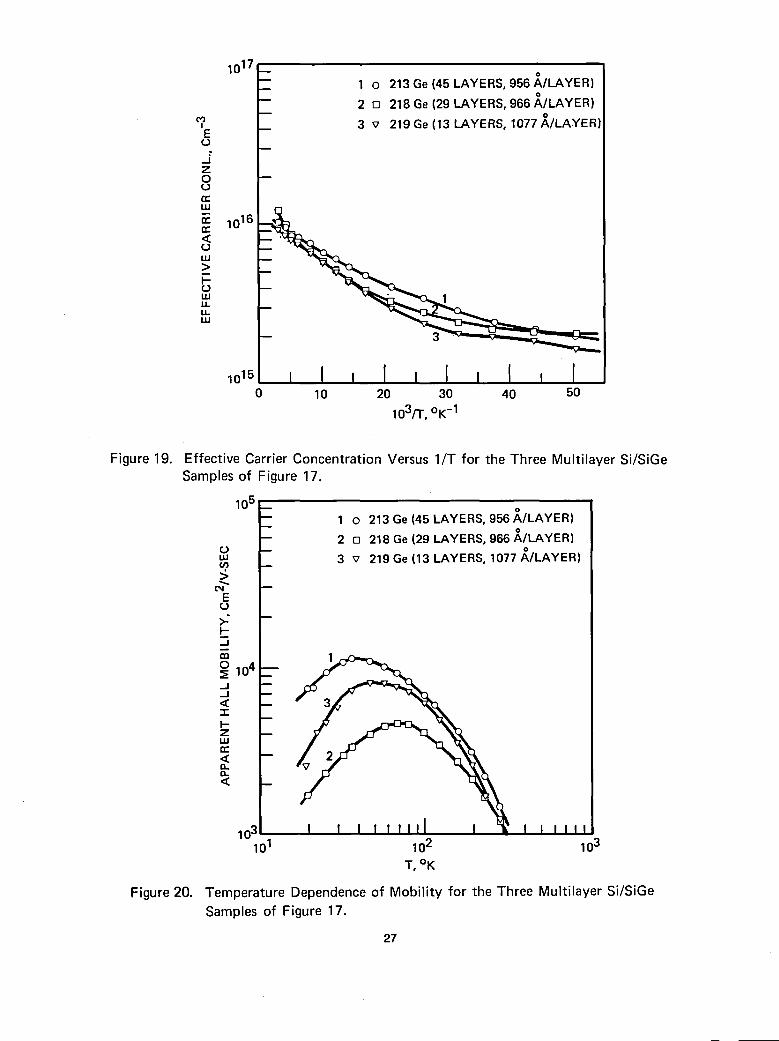
19. Effective Carrier Concentration Versus 1/T for the Three MultilayerSi/SiGe Samples of Figure 17 ..................................................... 27
20. Temperature Dependence of Mobility for the Three Multilayer Si/SiGeSamples of Figure 17 ................................................................ 27
21. Resistivity Versus 1/-I"for Two Multilayer Si/SiGe Samples Both Grownat 1004°C and with About the Same Total Thickness (-4.41_m) butDifferent Number of Layers ........................................................ 28
iv

ILLUSTRATIONS (Cont)
Figure Page
22. TemperatureDependenceofHallMobilityfortheTwoMultilayerSi/SiGeSamplesof Figure20 ................................................................ 29
23. ResistivityVersus1/'1"forMultilayerSi/SiGeSamplesContaininga2.4p.mP-TypeBufferLayerBetweentheSubstrateandthe Multilayer...................................................................... 30
24. Comparisonof TemperatureDependenceof HallMobilityforMultilayerSi/SiGeSampleswith(No. 194Ge) andwithout(No.219) Ge BufferLayer..................................................................................... 30
25. CarrierConcentrationProfileof SampleNo.29 .............................. 3226. CarrierConcentrationProfileof Sample48 at RoomTemperature..... 3327. TotalNumberof ElectronsPerUnitAreaina SuperLatticePeriodin
SampleNo.48 ........................................................................ 3328. CarrierConcentrationProfileof Sample48 at31°K ......................... 3429. CarrierConcentrationProfileof Sample48 at 21°K ......................... 3530. GatedHallDevice.................................................................... 3531. ChannelConductanceof Device324 as a Functionof GateVoltageat
77°K ...................................................................................... 3932. GateCapacitanceVersusGateVoltageof Device324 at 77°K .......... 3933. CarrierConcentration(X)andDriftMobility(I-:-I)ProfilesofDevice324at
RoomTemperature.................................................................. 4034. CarrierConcentration(X)andDriftMobility(FI) ProfilesinFilmNo.324
at 77°K ................................................................................... 4135. CarrierConcentration(X)andDriftMobility(I-:1)ProfilesinDevice231 at
RoomTemperature.................................................................. 4136. CarrierConcentration(X)andDriftMobility([]) ProfilesinDevice231at
77°K ...................................................................................... 4237. CarrierConcentration(X)andDriftMobility(l_) Profilesof Film231 at
30°K ...................................................................................... 4238. HallMobilityandCarrierConcentrationProfiles(BeforeData
Smoothing)of Device231 at 80°K ............................................... 4439. HallMobilityandCarrierConcentrationProfiles(AfterDataSmoothing)
of Device231 at 80°K ............................................................... 4540. C-V Curveof MOSCapacitorinSampleNo.42 ............................. 4841. AugerProfileof Si,Ge, andO inthe OxidizedMultilayerFilmNo. 136
(OxidizedinStreamfor30 Minutesat875°(3) ................................ 5042. AugerProfileof Si,Ge, andO intheOxidizedMultilayer
FilmNo.135 ........................................................................... 5043. AugerProfileof Si,Ge, andO inthe OxidizedMultilayerFilmNo.136
(OxidizedinSteamfor68 Minutesat 25°(3)................................... 51
V

ILLUSTRATIONS (Concluded)
Figure Page
44. Auger Profileof Si, Ge, and O in the OxidizedMultilayerFilmNo. 136(OxidizedinSteamfor300 Minutesat925°C) ................................... 51
45. A to F: ProcessingSteps Commonto BothMESFET and MOSFETDevices .................................................................................. 53
46. Ato DMOSFET ProcessingStepsFollowingStepsinFigure45 ............ 5547. A to C ProcessingStepsfoe MESFET Devices(FollowingStepsin
Figure45) ................................................................................ 5648 MESFET on Si/Si_.xGex Film No. 324, Gate Width = 40 i_m Gate
Lengths areX 36, 24, 8, and 4 i_m .................................................. 5749. I;D-VsD;Vg of MOSFET Devices ................................................... 5850. Ideal Energy BandDiagramof SiGe/Si Heterojunction ........................ 6251. Energy Band Diagram of SiGe/Si Heterojunction with
InterfaceStates ........................................................................ 6352. Hypothetical Energy Band Diagram of the Si/Si_.xGex
Heterojunction .......................................................................... 64
TABLES
Table Page
1. Characteristicsof Si: P, SiGe: P, and Si: P/SiGe: P FilmsAnnealedfor0.5 Min BetweenLayers ............................................................ 5
2. Effects of Substrate Orientation on Film Properties (Growth9
Temperature- 1000°C) ............................................................3. Si-Ge Alloy - X-Ray Strain Results ............................................... 164. X-Ray Strain Results of Thin Single Layer SiGe Alloy Films .............. 185. Summary of Parameters of Films Examined by TEM ....................... 196. Summary of Properties of Multilayer Si/SiGe Films Measured Below 20°
and 400°K ............................................................................... 267. C-V Measurements Data of Sample 124 ....................................... 49
vi

SECTION I
INTRODUCTION
The purposeOfthisprogramwasto exploresuperlatticestructures(i.e.ultrathinperiodicallylayeredsemiconductorheterostructures)in silicon-basedsemiconductorsand to explore thedeviceapplicationsin suchstructures.
Research in superlattice structures in IIl-V compound semiconductors (Ref 1, 2) resulted inthe discovery of new phenomena such as negative differential conductivity normal to thesuperlattice axis and enhanced electron mobility (Ref 2) due to the formation of a 2-dimensionalelectron gas at the heterojunctions in the superlattice. While the former was a direct result ofcoherent scattering of electrons by the superlattice potential, the latter phenomenon is in fact aheterojunction phenomenon and occurs even in a single selectively doped heterojunctionbetween two semiconductors with specific band structure line-up and doping profile (Ref 3).
Mobility enhancement was observed in MOS electron inversion layers as a result of the split-ting of the conduction band minima in the narrow energy well created by the application of thegate voltage (Ref 4). Si-based superlattice structures (Ref 5) specifically Si/Sil.xGex,were alsopredicted to exhibit electron mobility enhancement due to basically the same mechanism - thistime by the perturbation due to the superlattice potential.
Several schemes (Ref 6) have been proposed for the realization of superlattice structures insilicon by means of lithographic techniques. Another means of constructing a periodic structure isthe now familiar technique of epitaxial deposition of semiconductor thin films of different composi-tion but with small lattice mismatch. After reviewing the lithographic resolution requirements forsuperlattice structures where the electron mean free path (-300A) is comparable to thesuperlattice period, we decided to pursue the second approach of epitaxial growth of thinalternate layers of Si and Sil.xGex. The value of x was to be determined experimentally as evi-denced by the crystalline quality of the multilayer films. The method of deposition was chemicalvapor deposition (CVD) by the pyrolysis of Sill4 in an H2 atmosphere. The choice of the deposi-tion technique was dictated by the availability of a Silicon CVD System in our laboratories atMRDC. Although the molecular beam epitaxy (MBE) technique offers much better control of thelayer thickness, we thought the CVD technique should provide sufficient thickness control forfabricating the superlattice structure. In fact, films with individual layer thickness of about 300Ahad clear layered structure as seen with scanning electron microscopy (SEM) and Auger electronspectroscopy (AES) depth profiling.
The program evolved into several phases: the first phase was one of exploratory nature inwhich films with different parameters were grown and evaluated. The parameters that were variedwere layer composition (percentage Ge in the alloy layers), individual layer thickness, number oflayers, and growth temperature. The evaluation of the films consisted of measuring the conductiv-ity, carrier concentration, and mobility (Hall effect) at room temperature and 77°K, and examina-tion of the film cross section by SEM. The film composition was determined using energydisperive X-ray spectroscopy (EDXS) to measure the average film composition. Auger profilingand "secondary ion mass spectroscopy analyses were made for several films to determine thecompositional profile of the layered structure. During that phase we found that the Hall mobilitiesmeasured in multilayer films whose parameters are within a certain range were consistentlyhigher (sometimes by a factor of 50 percent) than those of single layer Si or SiGe films of compa-rable thickness and carrier concentration.
1

This finding led to the second phase of the program where systematic study of the effect ofthe film growth conditions on the film properties was made.The growth conditions that were stud-ied were the doping concentration, growth temperature, substrate orientation and the Ge contentin the alloy layers. A fairly large number of films were fabricated and evaluated. In parallel withthese activities, physical characterization of the films was performed in an effort to explain theobserved mobility enhancement in terms of the film structure. The film electrical parametersweremeasured from room temperature down to 20°K. X-ray double crystal diffraction rocking tech-nique was used to measurethe elastic strain, the strain relief, and the unstrained lattice constantsof the layers of the films. Transmission electron microscopy (TEM) examinations of some filmswere made.
The third and last phase of the program was to fabricate MESFET and MOSFET devices onsuitable multilayer films for integrated circuit applications and to use the devices to measure thelocal electrical properties of the film as a function of depth.
The results obtained from the analytic investigation shed considerable light on the cause ofthe observed enhanced electron mobility in these films and revealed very interesting features oftheir electronic structure. The results show electron confinement at the alternate interfaces of theSi and SiGe layers, namely, the interfaces with the SiGe on top of Si. The cause of this confine-ment is not yet clear although it might be due to the conduction band discontinuity at theheterojunction. The confinement then results in the splitting of the energy band minima of the con-duction band as descried by Moriarty and Krishnamurthy (Ref. 5) The resulting redistribution ofelectrons among the sub-bands leads to enhanced mobility for sufficiently low electron densityand large enough band splitting compared to the thermal energy kT. This can account for theobserved 40-50 percent mobility enhancement observed in these films.
This report is divided into six sections with the first being this introduction. Section II detailsthe film growth conditions and their effects on the film electrical parameters. Section III describesthe investigation of the film structure by various analytic techniques. Section IV describes theexperiments and results of the characterization of the electrical properties of the film includingthose obtained from the field effect transistors. Section V describes the device fabrication pro-cesses and Section VI contains discussion and conclusions.
The authors would like to acknowledge the contributions by Howard Glass (x-ray doublecrystal diffraction experiment), Jane Yang (Hall measurements), and Ilan Golecki (RBS meas-urements) and the skilled assistance of Sigfried Plonski, Jane Cooper, Roy Harada, NancyCasey, and Carol Sallee in device fabrication.

SECTION II
CVD GROWTH OF THE MULTILAYER Si/Sil.xGex FILMS
This section describes the film growth technique using chemicalvapor deposition (CVD)andthe effect of the film growth conditions on the film properties. We will discuss the properties interms of carrier mobility, carrier concentration, Ge content, and film appearance. The Van derPauw method was used to determine the resistivity and Hall coefficient from which the carrier con-centration (n) and mobility I_were deduced. The Ge content was determined by Energy Dispers-ive X-ray Spectroscopy (EDXS) and AES. The film thickness, which in turn determines thesuperlattice period, was measured using the SEM. Visual observationof the films during and aftergrowth gave indication of the film quality.
The CVD growth of the films employed hydrides as sources of Si and Ge. CVD growth ofSiGe alloys on Si using the halides was reported as early as 1962 by Oda (Ref 7) and Miller andGrieco (Ref 8) and in 1972 by Aharoni and co-workers (Ref 9), but films from the halides requirehigh growth temperatures (1100-1200°C) (Ref 9,10), and layer dopant interdiffusion would beexpected at these temperatures. In addition, the generated HCI would also be expected to causeproblems in composition and doping control of very thin layers due to a competing film-growth andetch-back process. On the other hand, epitaxial SiGe layers have been grown from the hydrideson Ge as low as 800°C (Ref 11) and on Si as low as 1000°C (Ref 12). We prepared Si and SiGealloy layers and films from one Sill4 source (5 percent in He) and two GeH4sources (5.5 percentin H2 and 5.5 percent in He) in a Pd-purified H2carrier gas on high resistivity single crystal p-typeSi substrates. Intentionallly added dopant species were from proportioned flows of phosphine(PH3, 45ppm in He) and diborane (B2H6,46ppm in He). Total gas flow was about 3 Ipm.
Apparatus
The films were grown in a CVD reactor system, a schematic of which is shown in Figure 1. Itconsists essentially of: (1) a reactant gas manifold and distribution line system of mostly 1/4 in.valving, filters and flow controls, (2) a vacuum pumping system for evacuating selected portions ofthe reactor system as needed, (3) provisions for burning the reactor exhaust gases, and (4) a75ram diameter vertical quartz deposition chamber with provision for supporting the substratesnormal to gas flow on a rotatable SiC-coated graphite susceptor. The susceptor is inductivelyheated by a radio frequency coil that surrounds the deposition chamber. An automatic sequencetimer with a mechanical counter in series is usedto control solenoid-activatedair-operated valvesfor rapid and precise flow control of the gases and reactants. Dopinggases were injected into theSill4 line. A separate line was used for the GeH4,with both lines joining near the top of the depo-sition chamber. Temperatures were measured with an optical pyrometer that was focused on theside of the if-heated susceptor. The actual temperature at the top of the susceptor is lower thanthe reported measured temperature by about 50°Cwhen the side-temperature is about 1000°C.
In the following we describe the experiments performed for investigating the effects of thegrowth conditions on the films properties.
Growth Temperature Studies
The initial phase of the experiments determined the minimumtemperature at which reasona-ble quality single-layer films of Si and SiGe could be grown in our system on (100)-oriented Sisubstrates. The temperature range 900-1000°C was examined; and based on the refiectivity and
3

VACUUM GAUGE TUBE BURN-OFt-_BOX
CONVENTIONALFLOW METERS
TIMER
'1CONTROL I
INPUT
CARRIER GAS
INPUTS J• MASS FLOW CONTROLLERS Sill4• VALVES INPUT
O GAUGES
Figure 1. SchematicDiagramof the Si CVD ReactorSystem
smoothness of these (100)-oriented films, 1000°Cwas established as a preferred growth temper-ature. As shown in Figure 2, during these early experiments it was found that the incorporation ofGe into the film was temperature dependent, i.e., more Ge was incorporated in the film at 900°Cthan at 1000°C for the same reactant gas flow rates. The wall deposit was heavy where SiH,-GeH4 mixtures were pyrolyzed, andthe growth rate was mainly influenced by the Sill4 flow at agrowth temperature of -1000°C. Si films were high resistivity, and SiGe films were n-type(-101%m "3)at growth rates of -0.31_m/min. At this growth rate and temperature the Ge molefraction was -0.08-0.10. By lowering the Sill, flow (from a value of 50 to 10ccpm), the filmsbecame p-type for rates of -0.11_m/min. using the original tanks of Sill, and GeH,. The filmsbecame more p-type as the Ge content increased (up to at least 9.27 mole fraction Ge), therebynecessitating the addition of an n-type dopant, phosphorus, to produce n-type films.
When a second tank of GeH. (-5 percent in He) was used in combination with the sametank of Sill4, the "undoped" SiGe films were n-type. It was also determined that single films of Siwere now n-type with n -1-2x1015cm"3 rather than high resistivity, as previously found. A seriesof multilayer growth experiments which repeated many of those performed with the first GeH.tank, but without PH3 additions, led to similar electrical results.
Table 1 compares the properties of phosphorus-doped single layer Si and SiGe films andmultilayered Si/SiGe films grown at the higher rate at three different temperatures. We note thatthe thicker -10 mole percent Ge films grown even as low as 900°C show comparatively highmobilities (-1350cm2/V-sec for n -101%m 3) even though the films are probably compensated.During the early stages of growth the films were gray, but they slowly changed in reflectivity as
4

6O
1000°C 1000°C iOoC 1000°C
g:_ _ 9ooocO0 40 900°c
°__ / 1000°C A 952124
oooiy = FLOW AT 50 ccpm
_O (5% IN He)u. 20
z O= Sill4 FLOW AT 10 ccpmo (SINGLE LAYER)
_ 1000°C O= Sill4 FLOW AT 10 ccpm
/ (SINGLE ALLOY LAYER0.5 MIN GROWTHINTERVAL)
o I I I I !0.10 0.20 0.30 0.40
X=(MF Ge)
Figure 2. Effect of GeH4 Flow and Growth Temperature on theFilm Composition of Sil_X Gex Alloy Layer
Table 1. Characteristics of Si: P, SiGe: P, and Si: P/SiGe: P Films Annealed for 0.5 Min BetweenLayers
APPROX. M.F. ROOMTEMP.SEQ. GROWTH FLOWS(ccpm)* GROWTH TOTAL NO. THICKNESS Ge RESIST ELECTRONCONC. MOBILITY
NO. TEMP (°C) SiH4-GeH4 TIME (MIN) OF LAYERS .urn A/LAYER (EDAX) (ohm-cm) (cm"3) (cm2/V-Sec)
15 -1000 50.0 25 1 8 - 0.23 3.5x10¹⁶ 784
16 -1000 50 -45 25 1 9 0.08 0.52 1.9x10¹⁶ 620
17 -1000 [50-0 0.2 20 1.2 600 1.1 1.7x1DTM 3471,50-45 02
23 _ 950 50-0 , 50 1 9 - 0.47 2.3x10¹⁶ 569
24 - 950 50-45 25 1 10 0.09 0.27 5.2x10¹⁶ 442
20 ~ 950 [50-0 0.2 100 5.2 520 0.43 I.lx1016 1330L 50- 45 0.2
11 - 900 50.45 25 1 10 _0.10 0.17 1.3x10¹⁷ 276(p-type)
0.4 100 6.6 060 0.26 1.6x10¹⁶ 146921 ~ 900 [50-0
L 50 -45 0.2
0.1 100 3.2 320 0.52 8.8x10¹⁵ 137039 ~ 90O [50-0I SO-45 0.1
they became thicker, ending as semi-reflective films. The thickness of each Si and SiGe layer wascontrolled by injecting the reactants into the deposition chamber for a specified time period. In thestudy, 0.5 min. was arbitrarily used between layer growths to purge the lines and reactor of resid-ual dopants and reactants. Thus, the lO0-1ayerstructure shown in Figure 3 was produced at950°C by 0.2 minute bursts of the silane source at 50ccpm and 0.2 minute bursts of the combinedSill. and GeH. sources, the latter at 45ccpm.

Figure 3. SEM Photograph of A 100 Layer Alternating Multilayer Si/Si.85Ge15Film, _' 5 #mThick. The Individual Si and SiGe Layers are "_ 500 _, Thick as Determined by an
Auger Profile.
Layer Thickness Dependence
The room temperature mobilities of thick multilayer Si/SiGe films grown at -1000°C at thelower growth rate (-0.11_m/min) using both GeH4 cylinders for Sil.xGexlayer compositions of x= 0.10 and x = 0.15 are shown in Figure 4 as a function of the Si layer thickness. In all cases, thethickness of the SiGe layer was either equal to or greater than that of the Si layer. The dopinglevels in the SiGe films are -1015cm3; in the Si, -10 is - 1016cm3. The data indicate highermobilities in the layered Si/SiGe films with 15 mole percent Ge in the SiGe layers for a Si layerthickness of _>400A.Good mobilities (-1000 cm2/V-sec)were found for multilayer films with Silayer thicknesses as thin as 250A.
In Figure 4, in the sequences 29, 53 and 54, the Si layer thickness was kept constant at-400A and the SiGe layer thickness was progressively increased from -400A to -1500A. Theresults (<10 percent mobility difference) indicate the thickness of the SiGe layer has little effecton the electrical properties of film grown under these conditionsof temperature, growth rate, layercomposition, etc.
Comparatively poor electrical results were obtained for layers grown with an injection time of0.2 min (-200A layer thickness). This may be due to a combination of insufficient gas mixing inthe reactor and layer inter-diffusion,for even the SEM at high magnificationwas unable to reveala layered pattern in such films.
Film Thickness Dependence
The electrical properties of the alternating Si/SiGe muttilayerfilms were found to be depend-ent on the total film thickness for films _<21_mthick. The results in Figure 5 includedata for two dif-
6

1500
O210 02651400 - ,231
o" 1300 - X =0.15IJJu? 53€:>_" 1200 0262E
1100._1m
o 1000)211 x=o, lo
uJn"--, 900 • 46I.-<_
'" 800a.
uJ='- 700
O FLOWSO,.,- 600 • = SiH4-GeH4 (10-20)
• = SiH4-GeH 4 (10-35)500
44
400 I I I f I I I200 400 600 800 1000 1200 1400 1600
Si LAYER THICKNESS IN SilSiGe MULTILAYER FILM (k)
Figure 4. Mobility Versus Si Layer Thickness in Si/Sil_X GeX Multilayer Filmswith X = 0.1 and 0.15. Layer Growth Rates Were _ 0.1 Per/Min at aGrowth Temperatureof "_ 1000oc. MeasuredCarrierConcentrationswere from 8 x 10¹⁵ to 3 x 1016cm-3. Total Film Thickness was between
2 gm and 6 gin.
ferent sets of films: one in which the Si layers are about 500A thick and the SiGe layers -1000Athick; and the other for films grown with layers of different thickness produced using the sameinjection times for the Si and SiGe layer in each film (from 0.3 min. to 1.5 min.).
The main feature observed in Figure 6 is that the electron mobility decreases steadily for filmthickness smaller than 1_m or thereabout. As will be discussed later, this is most likely due to theuneveness in the growth of the first few layers of the film. This was observed in the TEM examina-tion of the films and was also confirmed in the profiling of the electrical properties of the films.
Substrate Orientation Effect
Films were grown on (111) oriented substrates with film thickness about 0.25, 2.0 and4.0_m. The growth conditions were similar to those on (100) substrates. Table 2 provides a com-parison between the electrical parameters of those films to films grown on (100) substrates. Theelectron mobility in the (111) films is consistently smaller than the mobility in (100) films by a factorof 2 or more. This result, as will be discussed later, is consistentwith the proposed mechanism ofmobility enhancement which predicts that the enhancement should occur in the (100) and not inthe (111) oriented films.
7

2200
° I:UJ
2000- • SiI-- A Si Ge.J
O 1800 - Si/Si Ge> Si/Si Ge (WITH p-TYPE BUFFER)X
E 1600 -(J
>. x xA x x__ 1400 - x'---x
x,&x _% x&x _.
1200- xA x "
O e.._..._.._ x x
." 1000 - "_'_"e'_--_.a_ x x_
<I: • x x_"R'_e_"-_ o x %%1-r 800 x •,_ ._..Z •0 %
o -0_" 600 ---.._
" 40O _ _ -_'---- --"LU
200 -
0 I I I I I IIII I I I I IIIII I I I I Ittt
1015 2 4 6 8 1016 2 4 6 8 1017 2 4 6 8 1018
NET ELECTRON CONCENTRATION (Cm"3)
Figure 5. Electron Hall Mobility vs Net Carrier Concentration for (100)-OrientedSi (e),Sil. X Gex(_) , and Alternating Layer Si/SiGe (X, A) Films Grown Under SomewhatSimilar Conditions for X Between0.10 and 0.22 for Film ThicknessBetween2.0and 6.5/_m,and Si/SiGe Layer ThicknessBetween300,_ and 1500/_,.
Carrier Concentration Dependence
To determinethe propertiesof films of Si, SiGe, and multilayeredSi/SiGe (100)-orientedfilmsof differentelectronconcentrationlevels,a PH3-Hesourcewasproportionedandmixedwiththe Sill4 andSiH4-GeH4mixturesjustpriorto filmgrowth.The electricalresultsaresummarizedin Figure5 alongwithdata from manyotherfilmsgrownduringthe courseof the study,
The resultsshowa mobilityenhancementof from -20 percentto at least40 percentinthemultilayer Si/SiGe films over that of epitaxial Si layers and -100 percent over that of epitaxialSiGe layers for n from -8x10 is to -1017cm3.
Limited studies gave no indication that hole mobilities are enhanced in Si:B/SiGe:B
multilayers.On the other hand, low mobility values may be due to the fact that the B-doped p-typefilms are compensated by the n-type impurities present in the source gases.
Annealing Effects
Experimentswere made to explore the effect of extended annealing in H2 on film properties.The electrical parameters were first measured before annealing and a second time after anneal-ing. The annealing was performed at 1000°Cfor 2 hr in H2atmosphere. This extended annealingresulted in no change or a slight decrease in the electon mobility.
8

105
GO
oo •
........_" 104 --uJ -© Iu_ :E' -- I r,)
Z
a 8ILl
__ • _-
103 _ n" • • 1015_
---.5o
oo• ROOM TEMP.© I O 77°K
.-ln2 f I I I I I I I I I I t 10140 1 2 3 4 5 6 7 8 9 10 11 12
THICKNESS (/JM)
Figure 6. Carrier Concentration and Mobility Versus Thickness for UndopedMultilayer Si/Si Ge Films
Table 2. Effects of Substrate Orientation on Film Properties (Growth Temperature ~ 1000°C)
SEQ. SUBSTRATE FLOWS(ccpm) GROWTII TOTALNO. APPROX. RESIST. CARRIERC0NC. MOBILITYN0. ORIENT. SiH4-GeH4 TIME(MIN) OFLAYERS THICK(pm) (ohm-cm) (cm"3) (cmZ/V-Sec)
115 100_ 10-35 2.3 1 0.25 0.30 8.3x10TM 252111) 0.50 3.3x10¹⁰ 376
114 100_ 10-35 20 1 2 1.0 1.5x10¹⁶ 406111J 0.6 2.4x10¹⁶ 474
269 100" /10- 0 0.6 61 4.5 0.36 1.5x10TM 1165LIO-35 0.6 0.08 7,9x10¹⁵ 9462
111. flO -0 0.6 61 4.0 0.86 1.0x10¹⁶ 719LIO-35 0,6 0.33 5.6x10¹⁵ 3357
Buffer Layer Experiment
As mentionedearlier,multilayerfilmswithtotalthicknesslessthan1.0_mshowedlowermobilitiesthanthickerfilms.Thisobservationraisedthepossibilitythattheremightbe problemsassociatedwithgrowingdirectlyonthesubstratesurface.Experimentsweremadeto determinethepropertiesof thinfilmsgrownona bufferlayerof Siand/orSiGe.Tothisend,flowconditionsweresoughtusingB2H8inHe to producea P-typebufferlayerthatwouldjustcompensatethen-typeimpurityintheSiandSiGelayers.P-typealloyfilmsweregrownwithnetholeconcentra-
9

tions of -1016cm3 and resistivities as high as 4 _cm. Alternate P-type multilayer buffer Si/SiGestructures were then grown followed by thin n-type alternating Si/SiGe structures. Several films ofabout 1.0_m thickness showed electron mobility up to -1100 cm2/volt.sec compared to 800 to900 cm2/volt.secfor films grown directly on the Si substrates. Buffer layers of single layer p-Si andmultilayer Si/SiGe (also p-type) showed similar results. Thus, it appears that the buffer layerimproves the multilayer film quality as reflected in higher carrier mobility.
Summary
Enhanced electron mobility was found in n-type multilayer films under the following condi-tions:
1. Layer thickness between 300A to 1500A.
2. Total film thickness >l.0_m.
3. Growth temperatures between 950°C and 1025°Cwith a few good films grown at about900°C.
4. Alloy layer composition of 10 to 20 percent Ge.
5. Dopant concentration (or more accurately the average carrier concentration) from7x1015to 2x1017cm-3.
6. Substrate orientation (100), but not (111).
10

SECTION III
INVESTIGATION OF THE FILM STRUCTURE
In this sectionwe describe the experimentsperformed to determine the physical structureofthe multilayer films. Rutherford backscattering (RBS), Auger electron spectroscopy (AES), andsecondary ion mass spectroscopy (SIMS) were used to determine the Ge depth profile in thefilms. Energy Dispersive X-ray Spectroscopy (EDXS) providedthe average percent Ge in the film.X-ray double crystal rocking technique was used to determine the lattice constant, elastic strain,and strain relief in the Si and SiGe layers. Transmission electron microscopy (TEM) was used toexamine the crystalline quality of the film and its interface with the substrate. Scanning electronmicroscopy was used routinely to examine the film cross sections and in some cases the surfaceof the films and provided an accurate measurement of the film thickness and hence, the periodic-ity of the superlattice.
Germanium Depth Profile
Some of the early films were analyzed by RBSwhich provided a quantitative measurementof the Ge percent in the film and its profile with depth. Figure 7 shows an RBS plot of film No. 20.The plot is the number of counts versus energy of the back scattered o_-particles.Since Ge hashigher mass than Si, particles backscattered from Ge atoms will have a higher energy than thosescattered from Si atoms. Thus, the Ge content profile appears first at the right of the chart. Start-ing at about the fourteenth layer (seven Si and seven SiGe layers), the sum of the Ge and Si sig-nals causes a sharp rise of the count level. The periodicity of the Ge signal is very clear up to atleast 28 layers. Since the data are collected in parallel, the measurement should not be affectedby drift in the beam current. The fluctuation seen in the signal is thus most probably real and maybe due to fluctuation in the RF power during growth which has been noticed. The Ge contentmeasured by RBS is -10 percent.
The Auger depth profile is made by periodic measurement as the sample is being sputteredby argon ion bombardment. The nominal sputtering rate is abut 1000A/min. The silicon signalrather than the germanium peak was used. Although measuring the fluctuation of the principalconstituent is subject to magnification of errors, it was determined that this method would yieldbetter results by obtaining better signal-to-the-noise ratio since Ge has a very low Auger sensitiv-ity. Figure 8 shows the relative magnitudes of the Si and Ge signals of sample No. 20. The Gecontent of the alloy layers was determined to be 14.6 percent, which corresponds fairly well to the6.5 percent average Ge content of the multilayer structure determined by EDXS (the ratio shouldbe 2:1 if the multilayer film thicknesses are identical). Figure 9 is a plot of sputtering time vs SiAuger signal level and shows the fluctuation of the percent Si content of the first 14 layers ofSample No. 20 showing a slight reduction in signal level for the deeper layers, most likely due todrift in the electron beam current.
It appears from the AES data that there is a transitionregion at the layer interfaceswhere theSi content (hence also Ge content) changes gradually. The width of this transition region is about100A near the surface and increases to almost half the layer thickness at greater depth (seeFigure 9). The finite width of the transition region can be attributed to several factors: insufficientpurging of the reactant gases between the growth of each layer, insufficient reactant gas mixingwhen their flow is turned on after each purge period, or it may be an artifact of the profiling tech-nique as a result of mixing by recoil of target atoms (Si or Ge) during sputter etching. We tend to
11

• o
1500 --
."..°
uJZ ":.%
-r •
z I000 -- Oo
° _'-":_:,-L,o311 267)
Q
" • " ; 258'" 330 (242)_- w .... .. I
"• o°. • IZ(9 " "" " "" 11 272
• . • ePn_o /-- ¢Ib0 • Io
m _ 8". q,o _ 349 199)ILl • ,,r... ,,,,,!I--
.% 286 365(201)
ooo(/3
v 384 184) 417 (138)
41°(1v!xee
,bff ,..j _, l
•...,.,.-,,y• • o•
,n, %
o- I I I I I I I I" .... I200 400 600 800 1000 1200 1400 1600 1800
BACKSCATTERED ENERGY (KeV)
Figure 7. Rutherford Back Scattering Profile of Film No. 20. The Ge Signal of the First 14 Layers (Si and SiGe)is Seen at the Right; the Si Signal isadded to the Ge Signal at the Left.

AU3
Z
>" 0n- Ge= 14.6 at %<_ Arn-
Zw
Si 1000 1100 Ge 1200
tsp = 315 sec
I I I I I I I I I0 1O0 200 300 400 500 600 700 800 900 1000
ELECTRON ENERGY, eV
Figure 8. Auger Signal of Si and Ge in Film No. 20

#20 (RUN 2)
_F'_-D 100%Si _
, • • • . • _ : ". ; _ ! •5 • . . • •
_- !" _' :f - %_r, :, _ _ -,. ..: w,= tJ "|_o _ ;_U.U/O ol _ era" ,e m s
/NbqP • l •
" IM
x _a-I0- I0_- I";' I<uJ,,2-1
IIII
1-- IIII
0 I I It= 0 1000 A/DIV TIME, 1.0 MINUTES/DIVISION
Figure 9. Auger Signal of Si VersusSputtering Time For Multilayer Sample No. 20. Sputteringo
Rate is About 100 A/Min.

consider the later factor to be the dominant one in light of the broadening of the apparent transi-tion layer width with depth, since mixing caused by sputter etching increases with etch time.Furthermore, the data obtained from the carrier concentration profile experiment, to be discussedin the next chapter, favors the picture of well defined interfaces between layers, at least for theSiGe:Si interfaces (SiGe on top of Si). Another factor that was ruled out concerning the broad-ening of the transition region is elemental Si and Ge interdiffusion between layers. Calculationsbased on Ge diffusion in Si indicate the transition layer width should be less than 30A for thegrowth condition of the films.
SIMS analysis was made to examine the possibility of dopant (phosphorus) pile up at theinterfaces.This possibility was raised in conjunction with the results obtained from the carrier con-centration profile experiment. SIMS analysis showed no pile up of phosphorus or any otherdopant at the interfaces. The analysis, however, indicated that the phosphorus concentration inthe alloy layer is about 1/2 to 1/3 that in the Si layer in spite of the fact that the flow rate of phos-phorus was kept constant during the growth of both layers. This result might indicate lower incor-poration rate of the phosphorus atoms in the alloy layer due to the fact that the size of phosphorusatom is much closer to Si than Ge. Phosphorus atoms should thus fit more readily into the Si lat-tice than into the lattice of the SiGe alloy. Due to the relatively low concentration of dopants in thefilms (-1016cm3), each data point required considerable sputter time resulting in lower depthresolution. Dopant measurements were made at only a few points during the film analysis. The Siand Ge content were very well resolved. The data for Film No. 27 is shown in Figure 10. Again,the argument for the transition region between layers in AES also applies to SIMS.
Si
I
o
50 100 150 200 250 300
SPUTTER TIME (MINUTES)
Figure 10. SIMSProfile of SampleNo. 27
15
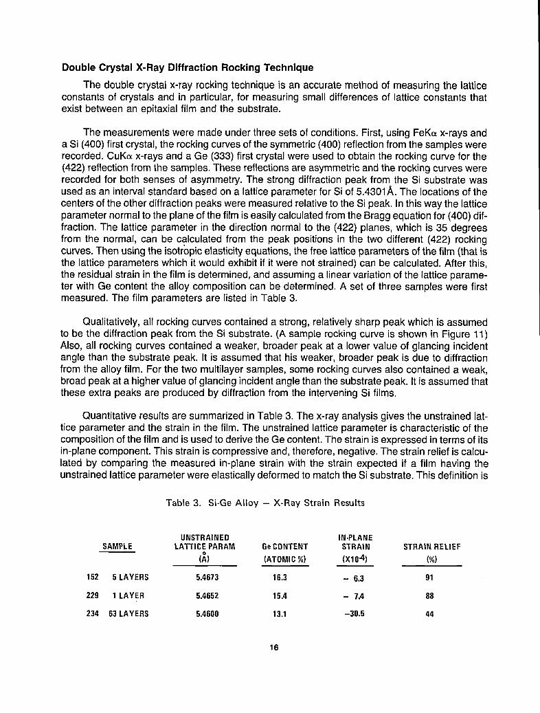
Double Crystal X-Ray Diffraction Rocking Technique
The double crystal x-ray rocking technique is an accurate method of measuring the latticeconstants of crystals and in particular, for measuring small differences of lattice constants thatexist between an epitaxial film and the substrate.
The measurements were made under three sets of conditions. First, using FeKo_x-rays anda Si (400) first crystal, the rocking curves of the symmetric (400) reflection from the samples wererecorded. CuKe_x-rays and a Ge (333) first crystal were used to obtain the rocking curve for the(422) reflection from the samples. These reflections are asymmetric and the rocking curves wererecorded for both senses of asymmetry. The strong diffraction peak from the Si substrate wasused as an interval standard based on a lattice parameter for Si of 5.4301A. The locations of thecenters of the other diffraction peaks were measured relative to the Si peak. In this way the latticeparameter normal to the plane of the film is easily calculated from the Bragg equation for (400) dif-fraction. The lattice parameter in the direction normal to the (422) planes, which is 35 degreesfrom the normal, can be calculated from the peak positions in the two different (422) rockingcurves. Then using the isotropic elasticity equations, the free lattice parameters of the film (that isthe lattice parameters which it would exhibit if it were not strained) can be calculated. After this,the residual strain in the film is determined, and assuming a linear variation of the lattice parame-ter with Ge content the alloy composition can be determined. A set of three samples were firstmeasured. The film parameters are listed in Table 3.
Qualitatively, all rocking curves contained a strong, relatively sharp peak which is assumedto be the diffraction peak from the Si substrate. (A sample rocking curve is shown in Figure 11)Also, all rocking curves contained a weaker, broader peak at a lower value of glancing incidentangle than the substrate peak. It is assumed that his weaker, broader peak is due to diffractionfrom the alloy film. For the two multilayer samples, some rocking curves also contained a weak,broad peak at a higher value of glancing incident angle than the substrate peak. It is assumed thatthese extra peaks are produced by diffraction from the intervening Si films.
Quantitative results are summarized in Table 3. The x-ray analysis gives the unstrained lat-tice parameter and the strain in the film. The unstrained lattice parameter is characteristic of thecomposition of the film and is used to derive the Ge content. The strain is expressed in terms of itsin-plane component. This strain is compressive and, therefore, negative. The strain relief is calcu-lated by comparing the measured in-plane strain with the strain expected if a film having theunstrained lattice parameter were elastically deformed to match the Si substrate. This definition is
Table 3. Si-Ge Alloy - X-Ray Strain Results
UNSTRAINED IN-PLANESAMPLE LATTICEPARAM GeCONTENT STRAIN STRAINRELIEF
o
(A) (ATOMIC%) (X10A) (%)
152 5 LAYERS 5.4673 16.3 - 6.3 91
229 1 LAYER 5.4652 15.4 - 7.4 88
234 63LAYERS 5.4600 13.1 -30.5 44
16

100 --
90 m
80
70 --
UJ
I--..% 60 --Q,..
,<w SILICON>F- 50 -- SUBSTRATE
PEAK_1
40 --
30 --
20 --
ALLOY LAYERS PEAK Si LAYERS PEAK
o _ IDIFFRACTION ANGLE
(1 DIVISION = 48 MINUTES OF ARC)
Figure 11. Rocking Curve of Sample 234 for Reflection Off the (422) Planes
17

not very accurate since the alloy layers are grown in Si layers that might be themselves elasticallystrained. Sample 234 was the only one to have very distinct extra peaks. These were observed inthe symetric and in one of the asymmetric rocking curves. If we assume that in the other asym-metric rocking curve the extra peak was hidden within the other peaks, then the extra peak can beascribed to the intervening layers of Si with a small amount (<3 percent) of Ge exhibiting in-planetensile strain of about 0.2 percent.
The quantities in the table are averages in the sense that the diffraction peak position is anaverage of the diffraction parameter of the film. To this extent,the uncertainty ineach quantity is inthe last significant figure shown. However, the diffraction peaks are fairly broad. The widths ofthese peaks could be due to a Ge content which varies from 13 to 18 percent and a strain whichvaries from -11 x 10.4to about zero.
This brings us back to the question of strain relief in the alloy layers which was calculated bysubtracting the measured in-plane lattice constant from that of the Si substrate. The actual strainrelief in a multilayer film, however, should be equal to the difference between the in-plane latticeconstants of the SiGe and the Si layers. In film No. 234 the average in-plane lattice constant is--5.4436A. This gives strain relief of only 16 percent rather than 44 percent as calculated previ-ously. It should again be pointed out that the strain distribution is quite large as seen in the widthof the diffraction peak and thus the above argument should be considered in light of this fact.
The data also indicate that the strain relief in a single alloy layer (film No. 229) and multilayerfilm with relatively thick alloy layers (No. 152) is considerably larger than that in the multilayer filmwith thinner alloy layers (No.234). This agrees well with published theoretical (Ref 13) and experi-mental (Ref 14) work indicating that thin epitaxial layers with small lattice mismatch to the sub-strate can be grown with few interface dislocation provided that they are thin enough. Interveninglayers of the same lattice constant as the substrate can leadto similar results as seen in the pres-ent case.
We thought of examining that question further by measuring the strain in the single layerfilms. Two samples with 500A alloy films were prepared. One film was grown on bare Si (No. 275)and the other (No. 277) on an epitaxial Si buffer layer grown immediately before it. The resultsshown in Table 4 confirm the conjecture that the strain relief is primarily affected by the layer thick-ness. Here the strain relief was even smaller than that of film No. 234. It should be pointed out thatthe uncertanty in the strain measurements is quite large (- _+20 percent) due to the broadness ofthe diffraction as illustrated in the rocking curve shown in Figure 11.
Table 4. X-Ray Strain Results of Thin Single Layer SiGe Alloy Films
UNSTRAINED IN-PLANE
LATTICEPARAM GeCONTENT STRAIN STRAINRELIEFSAMPLE (A) (ATOMIC%) (XlO4) (%)
275 5.4579A 0.122 -O.0041 +20%277 5.4588A 0.126 -0.0068 ..20%
18
TEM and SEM Examination
Severalfilmswereexaminedby transmissionelectronmicroscopyby Dr. D.K.Sadanaof theLawrenceBerkeleyLaboratory.The filmsexaminedare listedinTable5. A crosssectionimageofthemultilayerfilm No.234 is shownin Figure12. The firstfiveto sevenlayersclosestto thesub-stratearevery unevenandmightbediscontinuous.The layerstructurebecomesmoreevenawayfromthe substrate,eventuallybecomingregularand fairlyplanar.The unevenesscloseto thesubstrateinterfaceis consistentwiththe observationduringfilmgrowththatthe filmstartswithagrayishlookandgraduallybecomesmorereflectiveas thegrowthproceeds.Thisgrowthpatternis characteristicof initialgrowthnucleationin isolatedislandsthat grow and coalesceuntilthegrowthcoversthewholesurface.The unevenpartof the filmseen hereisaboutsevenlayers(Si+ SiGe)or about5000A. The observationthatthemobilityseen inthinfilms(<1.0l_m) isconsid-erablylowerthanthat inthickerfilmsmightbe dueto the unevennessof a substantialpart of thefilm in the thinnerfilms.
Table 5. Summary of Parameters of Films Examined by TEMTOTAL
GROWTHTEMP THICKNESS NO.OF _ p NFILMNO. °C MICRONS LAYERS CM2/VOLTSEC OHMCM CM"3
234 1002 4.5 63 1440 0.19 2.3X10¹⁶
250 1006 3.2 1 430 0.21 7.0X10¹⁶
The crystalline quality of the film seems to be fairly good with a moderate number of disloca-tions (marked by dotted lines in the picture). Figure 13shows a TEM picture normal to the plane ofa single layer film for a region close to the thinned out crater in film No. 250. Misfitdislocations areevident (straight crossed lines) along the [100] and [010] directions.
Typical surface morphology of the multilayer films is seen in Figure 14. Cross hatched sliplines are seen in all our samples and are thought to be generatedduring the cooling period of thefilm after growth due to the difference between the thermal expansion coefficientof the alloy layerand that of the Si substrate.
Summary
1. The multilayer film structureis seen to have fairly abrupt layer interfaces (<IOOA).
2. The dopant density (phosphorus) in the alloy layer is about 1/3 to 1/2 that in the Si layersindicating lower incorporation rate of phosphorus into the alloy layer than the Si layer dur-ing film growth. Within the experimental uncertainty of the SIMS technique, no dopantpile-up is observed at the layer interfaces.
3. The mismatch between the lattice constants of the alloy layer and Si is accomodatedthrough both elastic stain and strain relief defects (e.g., dislocations). The elastic strain,however, in multilayer or thin single layer alloy films is considerably larger than in thickalloy layers and consequently thin layered films are expected to have fewer dislocations.
4. The growth of the first layers of multilayer films appears to be uneven. This observationexplains the lower mobilities seen in thin multilayer films (<l.0_m).
19

l\)o
WAFERSURFACE
Figure 12. TEM Micrograph of the Cross Section of Film No. 234

Figure 13. TEM Micrograph Through a Thinned Section of Film No. 250. The Vertical andHorizontal Lines are Dislocations.

Figure 14. Microphotograph of the Surface of Film No. 172 Showing the Surface MorphologyNotice the Cross Hatch Pattern Along the (10D) and (010) DirectioTis
• 22
SECTION IV
ELECTRICALCHARACTERIZATIONOF THE FILMS
The organization of the material in this section follows the chronological order of the experi-ments performed. The investigation of the electrical properties started with Hall and conductivitymeasurements in the temperature range of 77°K to 400°K. These measurements gave an aver-age of the mobility and carrier concentration in the films. The results showed significant and unu-sual differences between the carrier concentration temperature dependence in the multilayersample compared to that in single layer Si or SiGe films. The measurements were extended tolower temperature (20°K) which revealed non-freezout of carriers. Experiments were then madeto determine the carrier concentration profile in the film using C-V measurement of Schottkydiodes fabricated on the films. This in turn showed very interestingfeatures in that the carrier con-centration (n) was strongly modulated with depth and that its peaks increased sharply at low tem-peratures. It also confirmed the carrier non-freezout which occurs at these peaks.
The above results prompted the design of an experiment to measure drift and Hall mobilitiesand the carrier concentration profiles in the film using what is known as a gated Hall device(GHD). This is simply a field effect transistor with tabs alongthe channel for measuring the poten-tial drop along the direction of the current flow, and normal to the current flow (Hall voltage). Themeasurements showed that the drift mobility is also modulated with depth and that the peaks arevery close to the peaks in the carrier concentration profile. The Hall mobility showed a similartrend, but with large data scatter. In all, the data gathered so far point to electron confinement atthe alternate layer interfaces and the possibility of mobility enhancement as a result of this con-finement as will be discussed in more detail later in this report.
Hall Mobility and Carrier Concentration Temperature Dependence
Hall measurements were made using the Van der Pauw technique. The samples were rec-tangular in shape and about 5 to 10 mm on the sides. The contacts were madewith indium dots inabout the middle of each edge. The indium contacts were alloyed for a few minutes at 400°C inN2. The measurements were made first between 77°K and 400°K in a set-up equipped with a liq-uid nitrogen dewar and with a resistance heater that surrounds the sample holder to control thetemperature. The results obtained for multilayer film No. 39, a single layer SiGe film No. 75, and asingle layer Si film No. 77, are shown in Figures 15, 16 and 17 respectively.
The Si and SiGe single layer films showed 'normal' behavior; i.e., the carrier concentrationremains constant over a range of temperatures where the donors are fully ionized, then it starts to
decrease as exp - z_E with z_E= 43 meV. Here we assumed that the semiconductor is not2kTheavily compensated, i.e.,
No > n >> NA.
The activation energy of the donors (AE) is much closer to that of phosphorus (P) in Si thanthe activation energy of P in Ge which is about 12 meV. This might lead to the conclusion that thedonor ionization energy is dependent only on the average alloy composition rather than the natureof the neighbors to the P atom.
23

J'+4"4"+ 4"4" 4- 4-+ 4- 4-
I I20 60 100 140
1/kT (1/eV)
Figure 15. Resistivity (+), Carrier Concentration (z_) and Carrier Mobility (o) in MultilayerSi/SiGe Film No. 39 (n-Si/SiGe on p-Si)
103 I I 1018-! 104
I I20 60 100 140
1/kT (1/eV)
Figure 16. Resistivity (+), Carrier Concentration (z_) and Carrier Mobility (o) of Single Layer SiGe
Film No. 75 (n-Si.85Ge.15 on p-Si)
24

103 i i 1018" 105
102 -- 1017_ 104o o o o o
E oo° LU,u o° ZE oo_c o IX:O >O o° UJ F-- ¢'4
°o _ <_-" E>- o tOI- 101 -++¢ _ _ _ i016-103 --
o++. O Z "-. >"_ U.I '- t--I- +o + "-"O _ -3b'_ ++ <] Z
o +++ ",-"O
'"s: _ ++++++o + + + + + O
v 100 _ _,,_,_,,_ _ 102
Ea = 0.044 eV
I I20 60 100 140
1/kT (1/eV)
Figure 17. Resistivity(+), CarrierConcentration(n) andCarrierMobility (o) of SingleLayerSiliconFilm No.77 ( n-SiEpion p-SiSubstrate)
Now lookingat the multilayerfilms,we foundthat n varies muchslowerat low temperature
thanin single layer films. In fact, theslopeof logn vs. 1.1.correspondsto an "activationenergy"of about 14 meV. kT
The measurements were extended to much lower temperaturesin a set up equipped with ahelium refrigeration unit capable of reaching 10°K at the sample holder. The results are summa-rized below:
The measurementswere made on five multilayersampleswhose physical properties,growthconditions and electrical properties at room temperature are summarized in Table 6. All fivesamples were grown at temperatures close to 1000°Cbut with different total film thickness andwith different total number of layers. Sample No. 194 contains a 2.5_m p-type buffer layerbetween the substrate and the Si/SiGe multilayer. The other four samples were grown directly onthe p-type (100) Si substrate. The electrical properties have been measured at room temperatureusing both the standard Hall measurement and Van der Pauwtechniques. There is a small differ-ence in the results of these two techniques as shown in Table 6. Such a small difference maycome from the inhomogeneity of the sample.
Temperature dependence of the resistivity measured between roomtemperature and 19.7°Kfor three multilayer Si/SiGe samples (No. 219Ge, No. 218Ge and No. 219Ge) is shown in Figure18. These samples were grown at 1002+-°C with approximately constant thickness per layer(-1000A/layer). The total number of layers are 45, 29 and 13 for No. 213Ge, No. 218Ge and No.219Ge, respectively. The most important result obtained in this investigation is that resistivity
25

Table 6. Summary of Properties of Multilayer Si/SiGe Films Measured Below 20° and 400°K
TOTAL LAYER GROWTH HALLEFFECT VAN DERPAUWSAMPLE THICKNESS NUMBER THICKNESS TEMP TIME N _ p N _NUMBER (_,M) LAYERS (P,) (oc) (MIN) 1016CM-3 CM2/V-SEC 0HM-CM 10TMCM"3 CM2/V-SEC 0HM-CM
194 1.1 21 523.8 1002 0.6 0.93 1453 0.4625
210 4.4 91 403.5 1004 0.4 1.093 1157 0.4942 0.865 1437 0.503
213 4.3 45 955.6 1004 0.8 1.02 1463 0.419 1.066 1382 0.424
218 2.6 29 965.5 1000 0.8 0.911 1212 0.666 1.102 1299 0.4362
219 1.4 13 1077 1002 0.8 1.24 1179 0.4274 1.10 1307 0.4344
101 _ 10 213 Ge (45 LAYERS, 956 A/LAYER)2 o
o 218 Ge (29 LAYERS, 966 A/LAYER)
3 A/LAYER)219 Ge (13 LAYERS, 1077
1001"_ 2
10-10 10 20 30 40 50
103FI",OK-1
Figure 18. ResistivityVersus 1/T for Three Multilayer Si/SiGe Samplesall Grown at 1002 +2°Cwith Approximately Constant ThicknessPer Layer (-_IO00A) but Different TotalNumber of Layers
changesverylittlebetween300°Kand19.7°Kforallfivesamplesmeasured.Thisslowchangeinresistivitywithtemperaturewasfoundtobea resultofnon-freezoutoffreecarriersat lowtemper-aturesas seen in Figure19. This resultis drasticallydifferentfroma typicaluniformlydopedn-typeSi semiconductor material. In general,ann-typeuniformlydopedbulkSi samplewithresis-tivityat roomtemperaturecomparableto the threesamplesabovewillhave almostsevenordersof magnitudechangeinresistivityinthesametemperaturerange.
The correspondingtemperaturedependenceof the Hallmobilitymeasuredfor the samethree samples is shownin Figure20. Forthesake of comparisononly,the Hall scatteringfactorwas takento beunity.
26
10171 o 213 Ge (45 LAYERS, 956.&,/LAYER)
2 o 218 Ge (29 LAYERS, 966 hJLAYER)
_E 3 _ 219 Ge (13 LAYERS, 1077 ,_/LAYER)
oo,,=,
1016
,,=
,0,_ I I _ I I I I I , I0 10 20 30 40 50
103/i -, OK-1
Figure 19. Effective Carrier Concentration Versus 1/T for the Three Multilayer Si/SiGeSamples of Figure 17.
105 m
1 o 213 Ge (45 LAYERS, 956 A/LAYER)
2 r7 218 Ge (29 LAYERS, 966 _/LAYER)
3 _ 219 Ge (13 LAYERS, 1077 _/LAYER)
oE
"7
_; 104
=<
103 I I I III101 102 103
T, OK
Figure 20. Temperature Dependence of Mobility for the Three Multilayer Si/SiGe
Samples of Figure 17.
27
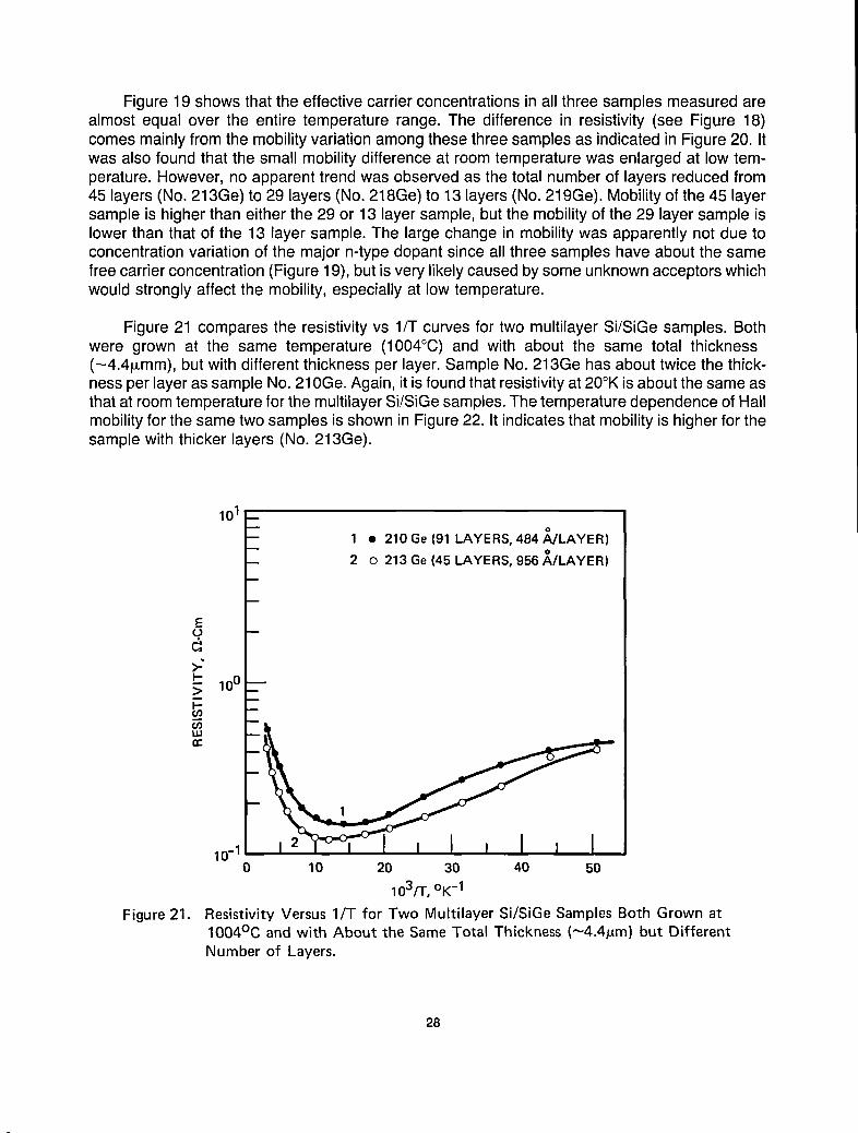
Figure 19 shows that the effective carrier concentrations in all three samples measured arealmost equal over the entire temperature range. The difference in resistivity (see Figure 18)comes mainly from the mobility variation among these three samples as indicated in Figure 20. Itwas also found that the small mobility difference at room temperature was enlarged at low tem-perature. However, no apparent trend was observed as the total number of layers reduced from45 layers (No. 213Ge) to 29 layers (No. 218Ge) to 13 layers (No. 219Ge). Mobility of the 45 layersample is higher than either the 29 or 13 layer sample, but the mobility of the 29 layer sample islower than that of the 13 layer sample. The large change in mobility was apparently not due toconcentration variation of the major n-type dopant since all three samples have about the samefree carrier concentration (Figure 19), but is very likely caused by some unknown acceptorswhichwould strongly affect the mobility, especially at low temperature.
Figure 21 compares the resistivity vs 1/T curves for two multilayer Si/SiGe samples. Bothwere grown at the same temperature (1004°C) and with about the same total thickness(-4.4t_mm), but with different thickness per layer. Sample No. 213Ge has about twice the thick-ness per layer assample No. 210Ge. Again, it is found that resistivity at 20°K is about the same asthat at room temperature for the multilayer Si/SiGe samples. The temperature dependence of Hallmobility for the same two samples is shown in Figure 22. It indicates that mobility is higher for thesample with thicker layers (No. 213Ge).
101 _
-- 1 • 210 Ge (91 LAYERS, 484 A/LAYER)o
-- 2 o 213 Ge (45 LAYERS, 956 A/LAYER)m
Eo,
>.-I-._ 100-
B
ooLUn_
-- 1
10-10 10 20 30 40 50
103/-I", °K-1
Figure 21. ResistivityVersus1/T for Two MultilayerSi/SiGeSamplesBothGrownat1004°C andwith About the SameTotal Thickness(_--4.4/_m)but DifferentNumberof Layers.
28

105 _m
1 • 210 Ge (91 LAYERS, 484,_,/LAYER)o
o 2 o 213 Ge (45 LAYERS, 956 A/LAYER)LU
>
Etj
m
m
0 104 2_,1._1<"I-I--zU.I
<o..
<
lo3 II III101 102 103
T,°K
Figure22. TemperatureDependenceof HallMobilityfor theTwoMultilayerSi/SiGeSamplesof Figure20.
Figure23 showsthe resistivityvs 1/T curveformultilayerSi/SiGesamplescontaininga2.5p.mp-typebufferlayerbetweenthesubstrateandthemultilayers.Thetemperatureinsensitiveresistivitymeasuredbetween298°Kand 19.7°Kagainwasfoundto be comingfrom a non-freezoutof freecarriersat lowtemperature.MobilityofthissampleiscomparedinFigure24withasamplewithoutbufferlayersandwitha filmthicknessperlayertwiceashigh.Highermobilityisfoundat lowtemperatureforthe samplewiththebufferlayer.
Insummary,themostsignificantresultobtainedinthemeasurementsisthatnon-freezoutoffreecarriersis observedforall fivemultilayerSi/SiGesamplesbeingmeasured.The followingtentativeconclusionsare alsoobtainedfromthelimitedsamplesbeingstudied:
1.Forsampleswithconstantthicknessperlayer,increasinglayernumbermayimprovefilmquality.
2. Forsampleswithconstanttotalthicknessdecreasinglayernumbermayimprovefilmqual-ity.
3. Sampleswithbufferlayersmayhavebetterfilmquality.
CarrierConcentrationandMobilityProfiles
Thenon-freezeoutofcarriersat lowtemperatureseeninmultilayerfilmsbringstomindthephe-nomenaof carriertransferacrosstheheterojunctionfromthehigherconductionbandsideto thelowerconductionbandside.ThisphenomenonoccursintheGaAs-GaAtAsheterojunctionandisresponsiblefortheobservedenhancedmobilityinthemodulationdopedheterostructure(Ref1).
29

101 __
-- • 194 Ge (21 LAYERS PLUS BUFFER,m O
524 A/LAYERS)
10-10 10 20 30 40 50
103/3-, OK-1
Figure 23. Resistivity Versus 1/T for Multilayer Si/SiGe Sample Containing a 2.5/_m P-Type BufferLayer Between the Substrate and the Multilayer.
105' _-- 1 • 194 Ge(21 LAYERS+ BUFFER,O
1.1 /Jm, 524 A/LAYER)L)I11
2 v 219Ge (13 LAYERS, 1.4_m,_, m o> 1077 A/LAYER)E
(.1
>: -I--_J-- 1O
104._I_.1
'-r"I--ZuJn"
n_
10301 102 103
T,°K
Figure 24. Comparison of Temperature Dependence of Hall Mobility for Multilayer Si/SiGeSamples with (No. 194 Ge) and without (No. 219 Ge) Buffer Layer.
3O

An experiment was thus made to determine the carrier concentration as a funtion of depthusing a capacitance-voltage measurement on a reverse biased Schottky or p. junction made onthe n-type semiconductor. The principle of the profiling is as follows:
The capacitance obtained in the C-V measurement is:
,o,o/0vdV dW
Where dQ is the charge stored in the semiconductor layer of width dW and dV is the change in theapplied voltage resulting in depletion layer width change dW, using the relations
c=AE and dQ=Aqn(w)W dW
where A is capacitor area, w is total depletion width, _ = Si or SiGe permitivity, q = electroniccharge, and n(w) is the carrier density which is a function of w, we can write
dl d 1(/ ca._(1) d [1 _/dV _ d [ w _/Aqn (w)=a"_'I,'_'!/ aw -8--w\_E j / c or _-_.c! =A2qcn(w)
1Thus n(w) can be determined knowing both _ and its derivative with respect to the bias voltage.
Now the value of n(W) obtained here is not equal to the free carrier concentration; rather it isequal to the free charge carrier density plus the change in the charges on the impurities andtrapping sites in response to the change of the applied voltage. At high temperature where thedonors are completely ionized, n then becomes equal to the free electron concentration. At lowtemperature where carrier freezeout is expected to occur, the interpretation of quantity n(W)becomes quite complicated since the charge contribution from the donors occurs at different loca-tions from the edge of the depletion layer (the Fermi level crosses the donor levels at finite dis-tance away from the depletion layer edge). At any rate n(W) sets an upper limiton the value of theactual free carrier concentration. In the following n(W) will sometimes be referred to as the carrierconcentration, however it is important to keep the above definition in mind.
Measurements were first made using the Lehighton ElectronicsMiller Feedback Profile Plot-ter Model 2000. Later measurements were made on a computerized set up using a Hewlett-Packard Impedence Analyzer Model 4192A for direct measurement of the capacitance as afunction of voltage.
Schottky diodes were fabricated on several films, some had Cr-Au and some had MoSi2metallization. The results are shown in Figures 25, 26 and 27 respectively. The measurement islimited from below by the depth of the depletion layer at zero bias and from above by the junctionbreakdown. At room temperature, n was modulated substantially with the peak to valley ratio of2.0 or more. The period of the carrier modulation coincided with that of the film (period = Si +SiGe thickness).
It was first thought that the maxima and minima corresponded to the SiGe or Si layer whichhave different doping when grown separately.This conjecture, however, turned out to be incorrectdue to several factors. One of them is the observation that the peaks become extremely sharp at
31
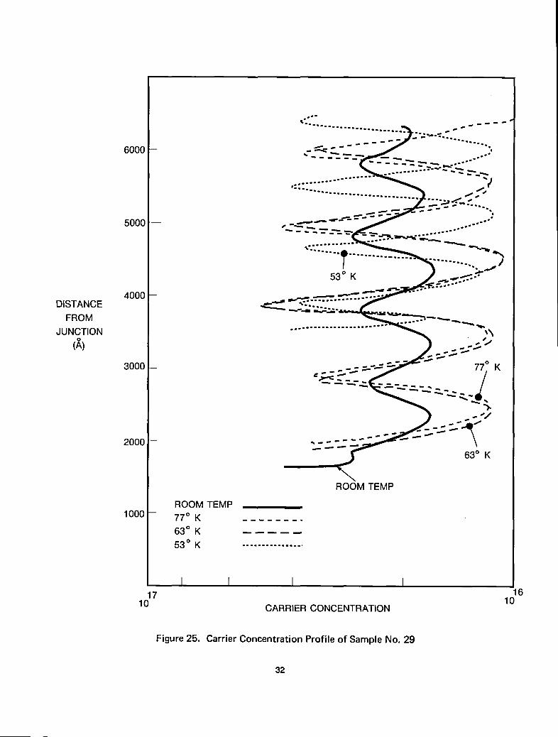
Figure 25. Carrier Concentration Profile of Sample No. 29
32

10,000
0 I I I I I I I I I
1018 1017 1016CARRIER CONCENTRATION
Figure26. CarrierConcentrationProfileofSample48 atRoom Temperature
X 10116.0
5.0 --_
0 4.0--I-
_-" 14°KZE,,,o 3.0 --
z<0'"
Z,_o _- 2.0--
_.luj1.0--
o.o I I I I I I I0 10 20 30 40 50 60 70 80
1000FF
Figure 27. Total Number of Electrons Per Unit Area in a Super Lattice Period in Sample No. 48
33

low temperature as shown in Figure 28 and Figure 29 which shows the evolution of the n distribu-tion as the temperature is lowered. This observation indicates that the peaks occur at well definedplanes in the film which are most likely the interfaces between layers. Assuming that to be thecase, by matching the profile of n to the known layer sequence of the film using the surface as areference point, the peaks were identified with the SiGe on Si interfaces. The alternate interfacesi.e., Si on SiGe, do not seem to correspond to any particular feature in the carrier profile.
At this point we considered two possibilities to account for these observations. The first is thetransfer of electrons across the heterojunction mentioned earlier. The second possibility is the fol-lowing: the Si and SiGe layers have fairly large mismatch in both their lattice parameters andthermal expansion coefficients. These are expected to cause large numbers of defects at thelayer interface and also in the bulk of the epitaxial layers. The defects can act as gettering centersfor impurity atoms resulting in dopant segregation to the interfaces.At higher temperature the car-rier distribution is relatively broad due to thermal diffusion of carriers away from the dopant atoms(Debye screening), and at lower temperature the distribution becomes narrower and morepeaked.
The next step in this investigation was the measurement of drift and Hall mobility profiles tosee if it could shed more light on the problem of determining the electronic structure of our films.The measurements are made using gated Hall devices (GHD) whose fabrication procedure ispresented in detail in the next chapter. The device is basically a Schottkyjunction field effect tran-sistor whose structure is shown schematically in Figure 30. All the pads except the gate haveohmic contacts. The gate (Pt silicide) covers the channel area and extends over to one pad (No.6). Pads 1 and 5 are connected to the voltage (or current) supply. The voltage drop along thechannel is measured between pads 2 and 4 (or 2 and 3). The Hall voltage across the channel ismeasured between pads 3 and 7.
10,000
o<
o_F- -
Z_ _
o 5000- '_"tr-
ILl(3z
I-- -
t-i
I
o ii I I II I i I1018 1017 1016
CARRI ER CONCENTRATION
Figure 28. Carrier ConcentrationProfile of Sample48 at 31°K
34

20,000
o,_v
zoF- -._1..)z _
10,000 -C)r_LL
LU€.)Z<I--U_
o '' , ' I11 , , I,, , ,1018 1017 1016 1015
CARRIER CONCENTRATION
Figure 29. Carrier Concentration Profile of Sample No. 48 at 21°K
GATE
2 3 4
I I
19 Lx =-I
Figure30. Gated Hall Device
35

The measurement of the drift mobility is made as follows: a voltage supply is connected topads 1 and 5 and the current (I) is adjusted such that the voltage drop between pads 2 and 4 issmall enough not to affect the depth resolution of themeasurement. For example, in our case
the built-in voltage - 0.8eV at Vg =0, AW ._/ q -2000 A/volt or an-1 016cm -3, and,_Vg "_2eN VbiVg
depth resolution of - 200A for V1, = 0.1 volt. At larger Vg the depth resolution improves further.The channel conductance at a given gate voltage is given by:
h
G = _qLy f # (z)n(z)dz, (1)Lx w
where h is the total film thickness and w is the depletion width given by the equation:
w
= q f zn(z)dz, (2)Vg + Vbi 7O
Differentiating (Eq 1) and (Eq 2) w.r.t. W we get
LydG = -q /l (w)n(w),and
(3)
dVg = q wn(w)dW e
dividing (Eq 3) by (Eq 4)
dG- eLy #(Vg) Ly_ = -__ _ (w) C(W) (4)dVg wL x Lx
where C(W) is the junction capacitance per unit area as measured by C-Vg technique.
The channel conductance is determined from the I-V measurement and is equal to:
115G - (5)
V24
36

Thus from G-Vg and C-Vg measurement the value of i_ as a function of gate voltage (ordepth) is obtained. Now, since the quantity n measured by the C-V technique represents an upperlimit for the free carrier density, the value of i_otherwise represents the lower limit for the actualdrift mobility.
The Hall mobility profile can be extracted from the measurements of V3z,V24as a functionof gate voltage as follows; In a film were the mobility F, the Hall factor VH, and carrier density nvary with depth the equations governing the Hall measurement are given by:
Jx(Z) = q/l (z)n(z)E x + q# H (Z)/I (z)n(z)EyB z (6)
Jy(z) = q # (z)n(z)Ey -- q # H (z) # (z)n(z)ExB z (7)
where i_and i_Hare the drift and Hallmobilitiesrespectively;their ratioFH/_is the Hall factorRH
which,we assume,is also a functionof z. Integrating(Eq 6) and (Eq 7) overz we get
Jx = q Ex/# (z)n(z)dz + q EyBz!# H (Z) # (z)n(z)dz (8)
Jy = qEyf. (z)n(z)dz - q Exgzf#" (z)# (z)n(z)dz (9)
where Jx and Jy are the sheet current densities.
Equating Jy with zero and substituting (Eq 9) in (Eq 8) we get neglecting the B2 terms:
-_xEY= Bz/H# (Z)/I (z)n(z)dz/! (z)n(z)dz/_ (10)
Jx /E_" = -_q /1(z.)n(z)dz (11)
Multiplying (Eq 10 and Eq 11) we get
h
JxEy / H (Z)_l,(z)n (z)dz (12)E2 = q Bz w _ "
37

The above quality is a function of the gate voltage through its dependence on W, the depletion'Ly 2
width. Multiplying by ([_-) we define the quantity Z(W)
Z(W) = IxV37 (Ly _2 /hV2 = q Bz /l H(z)/J.(z)n(z)dz (13)\Lx/24 w
differentiating w.r.t. W we get
H (W)_ (W)n(W) 114)Lx /\
combining Equations (14) and (3) we get
dZ = dZ / dG = BzLLy_#H(w) (15)d'--"G dVg _ _--_'x)
or
i (L dZ .do/_H (Vg)= B--z-" _ dVg (16)
Again the dependence of _1,H on Vg can be translated to a depth profile through the W-Vgrelation obtained from C-Vg measurement.
Drift Mobility and Carrier Density Profiles (Results)
The gated Hall devices were diced and mountedon DIP packages. The packages wereplugged intoa socketmountedon the coldfingerof the cryostat.Leadsconnectedthe sockettothe instrumentsoutsidethecryostatunit.The source/drainand gate biaseswere suppliedby theHewlett-Packard4140B digitalpicoammeterandvoltagesupplyunitwhichalso monitorsthedraincurrent.The voltagedrop along the channelV24was monitoredbya Hewlett-Packarddigitalvolt-meterModel3455B. The instrumentswere interfacedwitha microcomputerMINC (DigitalEquip-ment Corp) whichcollected,processedand plottedthe data as required.
Three devicesweretestedextensivelyin thisexperiment.The firstdevice(No. 324) wasfab-ricatedon a lp,m multilayerfilm with21 layers,the seconddevice(No. 231) was fabricatedon arelativelythickfilm (- 4.3_m) wth 61 layers,andthe thirddevice (No. 315) was fabricatedon a1p,mSi epitaxiallayer.
The data obtained for the channel conductance (per square) of device No. 324 as a functionof gate voltage is shown in Figure 31. The C-Vg measurement is shown in Figure 32. Both sets ofdata were taken at room temperature. The drift mobility and carrier density profiles extracted fromthese data are shown in Figure 33.
38

500.00
GSD
I I I I0 -1 -2 -3 -4 -5 -6 -7 -8 -9 -10
Vg (VOLTS)Figure31. ChannelConductanceof Device324 asa Functionof GateVoltageat 77° K
100PF
CG
0 -1 -2 -3 -4 -5 -6 -7 -8 -9 -10Vg (VOLTS)
Figure 32. Gate CapacitanceVersusGate Voltage of Device 324 at 77 OK
39
x DEVICE 324 (1/_m Si/SiGe)xROOM TEMP ._
A 6 -- Xo?, _-_ MOBILITYE(.o X CARRIER,.- ¢Jo 5 -- x CONCENTRATION -- 2000 ,,,
z :>o- _ Et- 4-- x -- (jn- >.I-z _:_ _--ILl L,.'-3 .--I
o 3- _z_ -- 1000z L_ Oon-I.U 2 -- --
n- L_rt-
1-- -- 0
I I × , I0.2 0.4 0.6 0.8 1.0
DEPTH (/_rn)
Figure33. Carrier Concentration(X) and Drift Mobility (E3) Profilesof Device324 atRoomTemperature
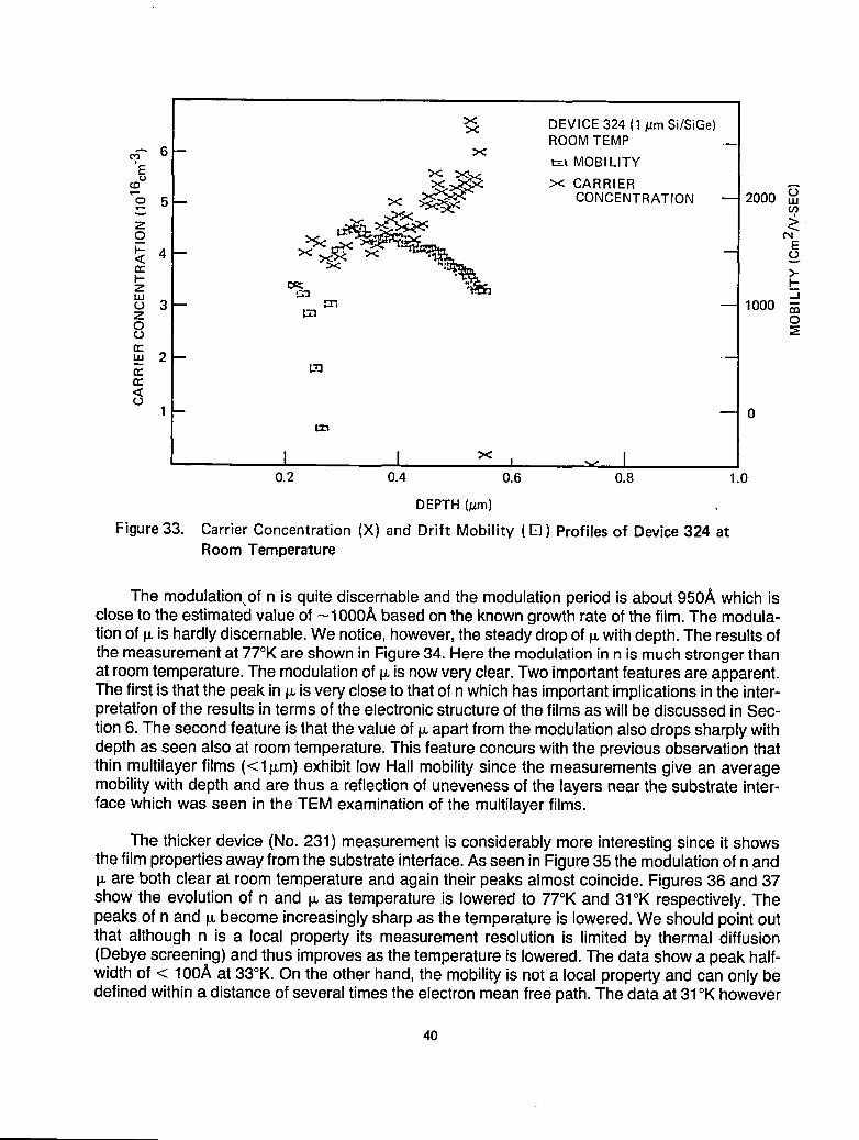
The modulation of n is quite discernable and the modulation period is about 950A which isclose to the estimated value of -IO00A based on the known growth rate of the film. The modula-tion of p,is hardly discernable. We notice, however, the steady drop of _ with depth. The results ofthe measurement at 77°K are shown in Figure 34. Here the modulation in n is much stronger thanat room temperature. The modulation of F is now very clear. Two important features are apparent.The first is that the peak in p,is very close to that of n which has important implications in the inter-pretation of the results in terms of the electronic structure of the films as will be discussed in Sec-tion 6. The second feature is that the value of p,apart from the modulation also drops sharply withdepth as seen also at room temperature. This feature concurs with the previous observation thatthin multilayer films (<lp, m) exhibit low Hall mobility since the measurements give an averagemobility with depth and are thus a reflection of uneveness of the layers near the substrate inter-face which was seen in the TEM examination of the multilayer films.
The thicker device (No. 231) measurement is considerably more interesting since it showsthe film properties away from the substrate interface. As seen in Figure 35 the modulation of n andp,are both clear at room temperature and again their peaks almost coincide. Figures 36 and 37show the evolution of n and p,as temperature is lowered to 77°K and 31°K respectively. Thepeaks of n and p,become increasingly sharp as the temperature is lowered. We should point outthat although n is a local property its measurement resolution is limited by thermal diffusion(Debye screening) and thus improves as the temperature is lowered. The data show a peak half-width of < 100A at 33°K. On the other hand. the mobility is not a local property and can only bedefined within a distance of several times the electron mean free path. The data at 31°K however
40

2.0 5000
_'_ x x1.8-- x ><
>< )<
-- 4000A 1,6-- ×op, x xE ×
X x
1.4 -- × x _ x
= x _: '"Z 1.2 -- x x × -- 3000× x x >0 x x ¢'qmI'- m x x E< 1.0 -- '-.-_'2n o
X _X X
z m _ -- 2000 --'" 0.8 -- mx m x .aL)
0 _=n 00.6 -- DEVICE 324 (1/_m Si/SiGe) _z_ .m
n- 77OK -_LU
0.4- _ MOBILITY _ -- 1000cc ,u_ CARRIER _t_ _.'_0.2 -- CONCENTRATION
I I I I I I I _ I 00 0.2 0.4 0.6 0.8 .0
DEPTH (/_m)
Figure 34. Carrier Concentration (X) and Drift Mobility (1_) Profiles in Film No. 324 at 77°K
20O02.0 x x
1.8 -- xX
X
1.6 -- ='< xxE(O _,ۥ-- 1.4-- =_,_xo _ .._ callm
m
x x Ex m "_ x _ _ 1000-- 1.0- m x_=r-xx
I-n" xx xX _ =_=' >-Z x X x I--LLI Xo 0.8 -- >< "JZ n_0 DEVICE 231 (4.3/_m Si/SiGe) O
0.6 -- ROOM TEMPn-w _ MOBILITYn- 0.4--m " CARRIER CONCENTRATION<
0,2--
I I I I I I I "1 I o0 0.2 0.4 0.6 0.8 .0
DEPTH (/_m)
Figure 35. Carrier Concentration (X) and Drift Mobility (I-q) Profiles in Device 231at Room Temperature
41
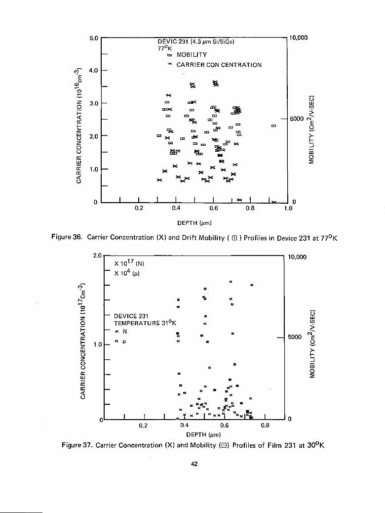
5.0 10,000DEVIC 231 (4.3/_m Si/SiGe)77°K
-- t= MOBILITY
CARRIER CON CENTRATION4.0-
E_o x =Jj_X_o
z 3.0 -- =a =_ ,,,
%, "_ r_ x _ '
F-- m m _'_ B mn- ==y_ m -- 5000I-- '-" ,-,1 ,-,1 E,",', €.JZ _ '-:, _ _n.u 2.0 -- "" x ,-,-, =_ _ _ >"o I.-Z m ,-,.,== _ =_ _ --
o -n.- o
n- X X x X
0
0 I I I I I I i_ I I_ o0.2 0.4 0.6 0.8 1.0
DEPTH (/_m)
Figure 36. Carrier Concentration (X) and Drift Mobility ( [] ) Profiles in Device 231 at 77°K
2.0 10,000X 1017 (N)
-- X 104 (/4J
o? =E
Bm
Z -- DEVICE 231 [] ,,,OO TEMPERATURE 31°K _
-- x N >< _ [] = 5000F.-- 1.0_ _ /J. x = 0Z,,, >-O I---Z -- '%O mt_ m ¢non" -- []LLI m
n,- m x _ =I:_ -- [] m m'_ X B X
0 [] _ x
0 I I I .1' "1" "_ " I_& a 00.2 0.4 0.6 0.8
DEPTH (/zm)
Figure 37. Carrier Concentration (X) and Mobility ([]) Profiles of Film 231 at 30°K
42

show the peak half-width of i_ to be about 200A. An estimate of the value of i_-10,000cm2/volt.secin Si gives a half-width of about 1200A at 30°K. This observation can be reconciledwith the experimental results if we assume large anisotropic mobility or (more likely) if electronsare confined in a energy well of dimensions less than the peak width of F. The peak value of t_isseen to reach 20,000 cm2/volt.sec at 31°K.
Hall Mobility Profile (Results)
The measurement of the Hall mobility profile is prone to errors for several reasons. Firstly,the Hall voltage is itself considerably smaller than the voltage drop along the channel for the mag-netic field available (5000 gauss) by a factor of 1/20 (for _ -1000 cm2/volt.sec). Secondly, thetime required for collecting the data is considerably larger than that of measuring the channel con-ductivity, since for each data point the magnetic field is reversedtwo times and allowed to stabil-ize for a few seconds. The result is higher chance of drifting in the measurements and morescatter in the results since the extraction of the values of _H involves taking differences betweenpoints. Typical results of the Hall mobility profile are shown in Figure 38 of sample No. 231 at80°K. Here we can see the relatively large scatter in the data, however the modulation of _H withdepth is visible. A program was written to smooth the data by recalculating each data point interms of the values of its five neighboring points. The results recalculated are shown in Figure 39.The results show that the _H profile is very similar to that of the drift mobility in that the peaksOflJ.H are very close to those of n. It also shows that _H is quite asymmetric in that its increase rateis much slower that its drop rate. Another feature is that the average mobility in the layers probedis considerably larger than that averaged over the whole film. For example, at room temperaturethe average i_Hover the whole film is about 1350 cm2/volt.sec. On the other hand, i_Hover thefew layers being probed is between 1300 and 2000 cm2/volt.sec.
Summary
The highlights of the results reported in this chapter are:
1. Carrier non-freezout occurs in the multilayer films at low temperature.
2.The carrier concentration profile shows large peaks at low temperature where thenonfreezout occurrs.
3. The electron mobility (both drift and Hall) is also modulated with depth. Mobility peaksalmost coincide with those of the electron concentration. These peaks are identified withthe alternate layer interfaces (SiGe on Si).
43

8E3
6>
E •
>_ ."4
-J
o
2
oioo Io2 Io4 Io6 08DISTANCE FROM Au/Si INTERFACE,/lm
5E16
3.75
E(J._ 2.5xz
1.25
ootoo Io2 Io4 Io6 08DISTANCE FROM Au/Si INTERFACE,/_m
Figure 38. Hall Mobility and Carrier Concentration Profiles (Before Data Smoothing) of Device 231at 80°K
44

8E3
6
o"
Eo
>." 4 • ..... _.... lI-
O
2
0 I I I0.0 0.2 0.4 0.6 0.8
DISTANCE FROM Au/Si INTERFACE, p.m
5E16
3.75
03IE
L_2.5
X °°
Z
°o
1.25 • .
oooo.o Io.2 Io.4 1o_ o.'_DISTANCE FROM Au/Si INTERFACE,/zm
Figure 39. Hall Mobility and Carrier Concentration Profiles (After Data Smoothing) in Film No. 231at 80°K
45
(Reverseof this Pageis Blank)


SECTION V
DEVICEFABRICATION
In this section we present the fabricationprocessesof the MESFET and MOSFET deviceson multilayer Si/SiGe and single epitaxial Si layers on p-Si substrates, and the results of thedevice characterization. We also discuss the oxidation experiment performed on multilayer filmsand the results obtained in the characterizationof the resultingoxide. Since the oxidation experi-ment chronologically preceded the FET fabrication we will start with the oxidation experiment.
Oxidation of Multilayer Si/Sil.xGexFilms
The aim of this experimentwas to evaluatethe oxidegrownon multilayerfilms.Boththinoxide(500-1000A) forpotentialuseas a gate insulatorinMOSdevices,andthickoxide(>2000A)whichcouldbe suitablefordeviceisolation(LOCOS)were examined.Two waferswere usedinthisexperiment.One (No. 142) has three alternatelayersstartingand endingwith Si layersof500A eachsandwichinga 2000A thickSiGelayerfora totalepithicknessof -3000A. Thesecondwafer (No. 136) had five layers(500A Si alternatingwith 2000A SiGe) for a total thicknessof-5500A. The experimentwas performedin twoparts.The firstpartwasto growa thinoxideonthe topSi layerof thewafer,whichat about500A thicknessshouldbe sufficientto growanoxidelayerslightlythickerthan 1000AwithoutconsumingtheunderlyingSiGe layer.The secondpartofthe experimentwas to growoxide filmsof differentthickness,startingwiththe same substrate,andto examinethe productof the oxidationprocess.
WaferNo. 142 wasoxidizedat875°Cinwet 02 for60 minuteswiththe targetSiO2thicknessof about1000A. The oxidationwas followedby annealingin dry N2for 30 minutes.The oxidethicknesswas 1040A, measuredwithan ellipsometer.MOS capacitorswere then fabricatedonthewaferusingthe followingprocedure.A maskof 50 milsquaredotpatternwasappliedandtheoxidewas etched outsidethe dots. Phosphorusimplantationwas made(80 keV, 1.2x1015cm"2)to forman n+ meshto act asthe returnelectrodefortheepilayer.(The substrateis p and isthusnot suitablefor electricalconnectionto the n-typeepi.) The photoresistwas removedand thewaferwas annealedat 875°C for30 minutes,to activatethe phosphorusimplant.An aluminumfilm(_8000A) wasdepositedoverthewafer.A maskwas appliedwith25 mil dotsinsidethe 50mil oxide patternand the aluminumwas etched off outsidethe 25 mil dots. The wafer was sinteredat 450°C for 15 minutes in forming gas.
The second experiment was to divide wafer No. 136into four quadrants. Quads 1 and 2 wereoxidized in steam at 875°C for 30 and 60 minutes, respectively. Quads 3 and 4 were also steamoxidized at 925°C for 68 and 300 minutes, respectively. The oxide thickness that should beobtained for Si under the above conditions are 500, 1000, 2000 and 5000A, respectively.
The ellipsometricmeasurementof theoxideswas successful only for the first two films. Thelast two films (Quads 3 and 4) gave readings that did not correspond to real solutions of a homo-geneous dielectric over a Si substrate. The oxide thickness on Quads 1 and 2 were 540A and1015A, respectively. The thickness of the oxides on Quads 3 and 4 was measured by etching astep and measuring the step height using a stylus profilometer.The steps were 2200 and 2500A,respectively.
47

C-V Measurement of the MOS Capacitors and Voltage Breakdown of the Oxide
The C-V measurements were made at room temperature. The plot shown in Figure 40 istypical of what is obtained within the central portion of the wafer (-1 in. diameter). Outside thecentral part of the wafer, the plot was flatter, indicating lower doping level. The C-V data was fedinto a computer program to calculate the interface state density and the results were tabulated inTable 7. The program was designed to handle uniformlydopedsemiconductorswhich was not thecase for our film. However, for an order of magnitude estimate of the interface state density thisseems like a reasonable choice. Here the density of interfacestates at the midgap is of the orderof 1011 cm2V -1, which is fairly reasonable for oxides grown in a steam atmosphere. SeveralMOS diodes were stressed for breakdown which occured at about 50 volts, or about 5 x 10⁶V/cm. A good thermal SiO2 usually breaks down at about 107V/cm.
Auger Analysis of the Oxide on Si/SiGe Films
The quadrants of Wafer 136 were analyzed using Auger spectroscopy inconjunction with ionmilling to determine the composition as a functionof depth. The procedure involves ion milling fora period of time then scanning the electron energy to determine the various elements present,then repeating the procedure over again. The results for Quad 1 to 4 are shown in Figures 41through 44. Quads I and 2 show no trace of Ge in the oxide up to the semiconductor interface anda few hundred A beyond. This is not surprising since only part of the uppermost Si layer isconsumedduring oxidation. ForQuads 3 and 4 the oxide also does not show any Geto within thesensitivity limit of the instrument which is only a few percent. However, a large Ge peak occurs at
1.0
DATE:6-9-83 • _ "=•
DEVICE NO.: 142Ge e_• • • • EXPERIMENTAL __,_/"
-- =
wax 0.5O
_J_J
0 I I
-5.0 -4.0 -3.0 -2.0 -1.0 0.0 1.0 2.0GATE VOLTAGE (V)
Figure40. C-V Curveof MOSCapacitorin SampleNo. 42
48

Table 7. C-V MeasurementsData of Sample124
YG C CS YG-YGFB ES-EF DF+DIT BIT(Y) (PF) US (PF) (Y) (EY) (NO./CM2) (NO.]CM2EY)
-5.0 78.7 -33.40 199.6 .4.94
-4.5 78.7 -33.13 199.6 -4.44
.4.0 78.9 -32.81 200.9 -3.94
-3.5 79.9 -29.91 207.1 -3.44 -0.395 1.21E+10
-3.3 80.8 -28.31 213.3 -3.26 -0.354 8.07E+09 9.84E+10
-3.1 82.0 -26.16 222.2 -3.10 -0.299 9.78E+08 1.28E+11
-2.9 83.4 -24.00 232.4 -2.94 -0.243 -8.38E+09 1.69E+11
-2.7 85.0 -21.56 245.5 -2.76 -0.181 -1.30E+10 7.37E+10
-2.6 85.9 -20.44 252.8 -2.68 -0.152 -1.62E+10 1.12E+11
-2.5 86.8 -19.17 261,4 -2.58 -0.119 -1.70E+10 2.27E+10
-2.4 88.1 -17.67 272.9 -2.47 -0.081 -1.35E+10 -8.97E+I0
-2,3 89.4 -16.22 285.8 -2.35 -0.043 -1.01E+10 -9.15E+10
-2.2 90.8 -14.67 301.1 -2.22 -0.004 .4.29E+09 -1.46E+11
-2.1 92.1 -13.41 316.3 -2.11 0.029 -2.44E+09 -5.70E+10
-2.0 93.4 -12.28 331.9 -2.01 0.058 -2.36E+09 -2.83E+09
-1.9 94.8 -11.16 349.4 -1.91 0.087 -1.54E+09 -2.84E+10
-1.8 96.2 -10.08 369.8 -1.80 0.114 -7.85E+08 -2.73E+10
-1.7 97.7 -9.00 393.5 -1.70 0.142 9.11E+08 -6.13E+10
-1.6 99.4 -7.95 422.5 -1.58 0.169 3.23E+09 -8.56E+10
-1.5 101.3 -6.89 458.2 -1.47 0.196 6.89E+09 -1.35E+11
-1.4 103.3 -5.86 503.4 -1.34 0.223 1.17E+10 -1.80E+11
-1.3 105.6 -4.86 562.0 -1.21 0.248 1.76E+10 -2.32E+11
-1.2 107.9 -3.94 635.6 -1.08 0.272 2.41E+I0 -2.73E+11
-1,1 110.3 -3.11 725.6 -0.95 0.293 3.06E+10 -3.03E+11
-1.0 112.5 -2.36 837.2 -0.81 0.313 3.74E+10 -3.55E+11
-0.9 114.6 -1.70 968.5 -0.68 0.329 4.40E+10 -3.93E+11
-0.8 116.4 -1.16 1110.4 -0.56 0.343 4.88E+10 -3.44E+11
-0.7 118.0 -0.67 1275.4 -0.43 0.356 5.40E+10 .4.21E+11
-0.6 119.3 -0.25 1450.1 -0.31 0.367 5.88E+10 -4.36E+11
-0.4 121.4 0.43 1829,2 -0.07 0.384 6.62E+10 -4.23E+11
-0.2 122,8 0.95 2211.8 0.14 0.397 6.94E+10 -2.41E+11
0.1 124.3 1.56 2831,3 0.46 0.413 7.34E+10 -2.51E+11
0.6 125.7 2.24 3775.4 0.92 0.431 6.42E+10 5.27E+11
1.1 126.5 2.71 4633.8• 1,31 0.443 4.25E+10 1.82E+12
1.6 127.0 3.03 5379.0 1.64 0.451 7.70E+09 4.17E+12
49

100
SAMPLE136-1
8O
2O
o I GeI I I I2 4 6 8 10 12 14o
OXIDE MILLING TIME IN MINUTES (1 MIN _ 100A)SURFACE
Figure 41. Auger Profile of Si, Ge, and O in the Oxidized Multilayer Film No. 136. (Oxidizedin Steam for 30 Minutes at 875°C)
lOO
SAMPLE 136-2
Si80--
o I I I I I Ge I IOXIDE 2.5 5.0 7.5 10.0 12.5 15.0 17.5 20.0'
SURFACE MILLING TIME IN MINUTES (1 MIN _ 100_,)
Figure42. Auger Profileof Si, Ge,andO in theOxidizedMultilayerFilm No. 136. (OxidizedinSteam for 60 Minutes at 875°C)
50

100
SAMPLE136-3
20 -- _1_ 12%Ge
\o I I I I I I
i 5 10 15 20 25 30 35 40OXIDE SURFACE MILLING TIME IN MINUTES (1 MIN_100A)
Figure43. Auger Profile of Si, Ge, and O in the Oxidized Multilayer Film No. 136 (OxidizedinSteamfor 68 Minutesat 925°C)
80SAMPLE136-4 Si
0
60
zO
_)
40 Ge
O Si€_) N
.J
20
o l 1 1 1 10 _0 20 30 40 5o 60 70!
MILLING TIME IN MINUTES (1 MIN _ 50 ,_,)OXIDESURFACE
Figure44. Auger Profile of Si, Ge,andO in the OxidizedMultilayerFilm No. 136 (OxidizedinSteam for 300 Min at 925°C)
51

the oxide semi-conductor interface indicating pile-up of Ge at that interface. This result is in agree-ment with published data about the oxidation of SiGe alloys (Ref. 15). It is thus advisable to limitthe oxidation of the multilayer films to the uppermost Si layer which should be of sufficient thick-ness for growth of the oxide. In cases where the required thickness of the uppermost Si layer isincompatible with the device structure, deposition of oxide might be useful.
MESFET AND MOSFET DEVICE FABRICATION
The first device lot was based on an existing mask set designed originally for GaAsMESFETs. A process compatible with the mask design involves metal liftoff for the source/draincontacts and for the Schottky metal gates. This attempt was abandoned due to unsuccessful lift-off caused by poor adhesion of the metal to the semiconductor surface. A new mask set wasdesigned and generated using an in-house electron beam exposure system (Cambridge EBMF).The mask set was designed for fabricating both MOSFET and MESFET devices using only fivemask plates of which three are common for both devices. The processing steps, unlike the liftoffprocess, allow for rigorous cleaning to be performed before metal deposition. The device fabrica-tion was successful on the first attempt and produced good working devices with characteristicsclose to those anticipated from the device design parameters and film properties.
The device lot contained 15 wafers: eight wafers with Si/SiGe multilayer epitaxial films, andseven wafers with n-Si epitaxial films. All epitaxial films were about 1.0_m thick. The nominal car-rier concentrations in the Si/SiGe films were about 1.0x1016cm-3 and in the Si films were about2.5xl 016cm'3.
The 15 wafers went through the processing steps common to both the MOSFET andMESFET devices and then the lot was split into three groups: a group of four wafers (two SiGeand two Si) for MESFET device fabrication, four wafers (two SiGe and two Si) for MOSFET devicefabrication, and seven wafers for backup. A step-by-step description of the fabrication procedurefollows: (see also accompanying illustration in Figure 45.)
1. The wafers were first cleaned using the standard silicon acid cleaning procedure(sulphuric-peroxide, HF dip and hydrochloric-peroxide bath). The wafers were thenloaded in the oxidation furnace. The oxidation cycle was 15 min. NV, 10 min. H2 + 02and 20 min. N2,all at 875°C. The oxide thickness was measured using ellipsometry andwas equal to - 200A. The oxide provided good surface adhesion for photoresist and alsoserved to protect the semiconductor surface during the subsequent steps.
2. The wafers were coated with photoresist (1350J at 3000 rpm) which provided a 2.5p.mthick layer. The photoresist was patterned to define the device area (Mask No. 1).
3. The oxide outside the device area was etched in buffered HF. The wafers were thenloaded into a parallel-plate plasma etcher and about 5000A of the semiconductor wasetched off using a CF4-O2plasma.
4. The photoresist left on the wafers was measured and found to be of insufficient thicknessfor the next step, and thus the wafers were repatterned using the same device area maskused before (Mask No. 1)
5. Ion implantation of boron was made at 25, 70, and 160 keY each with a dosage of 2x10¹²ions/cm2. The last two steps, namely the etching of the top 5000A of the semiconductorand the boron implant, provided the device isolation to a depth exceeding the epi thick-Bess.
52

OXIDE
OXIDE I n IP I I P
n-Epi j i
Pp-SUBSTRATE
• ANNEAL AT 1000 °C FOR 10 MIN TO• THERMAL OXIDATION (500,_) 925°C ACTIVATE THE BORON IMPLANT
--a-- -- d --
PHOTORESIST
W/y///AI n-E.i I J_{'._N_+J. L_N_+ ....... J L.
P
• APPLY ACTIVE AREA MASK• ETCH OXIDE • ETCH OXIDE
• APPLY SOURCE/DRAIN MASK• PLASMA ETCH 0.5/.{m N Epi • IMPLANT PHOSPHORUS1 X 1015 Cm-2
- b - 60 AN D 150 KeV
-e--
PR
V////////A /I I fiN+ I ' '
P I n I P P I _---- "J n _,-_. _ pJ I- .I L.
P P
o
• IMPLANT BORON 2 X 10¹⁵ Cm-2 AT • DEPOSIT 5000 A LPCVD OXIDE AT 900°C (ALSO25, 70, 170 KeV PHOSPHORUS ACTIVATION)
--C-- --f--
Figure 45. A to F: ProcessingSteps Common to Both MESFET and MOSFET Devices
53
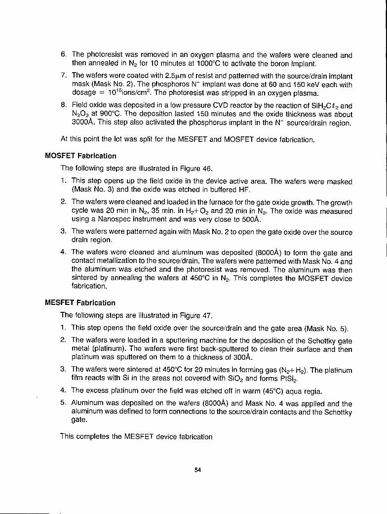
6. The photoresist was removed in an oxygen plasma and the wafers were cleaned andthen annealed in N2 for 10 minutes at 1000°C to activate the boron implant.
7. The wafers were coated with 2.51_mof resist and patterned with the source/drain implantmask (Mask No, 2). The phosphoros N. implant was done at 60 and 150 keV each withdosage = 1015ions/cm2. The photoresist was stripped in an oxygen plasma.
8. Field oxide was deposited in a low pressure CVD reactor by the reaction of SiH2C_2 andN203 at 900°C. The deposition lasted 150 minutes and the oxide thickness was about3000A. This step also activated the phosphorus implant in the N. source/drain region.
At this point the lot was split for the MESFET and MOSFET device fabrication.
MOSFET Fabrication
The following steps are illustrated in Figure 46.
1. This step opens up the field oxide in the device active area. The wafers were masked(Mask No. 3) and the oxide was etched in buffered HF.
2. The wafers were cleaned and loaded in the furnace for the gate oxide growth. The growthcycle was 20 min in N2, 35 min. in H2+02 and 20 min in N2. The oxide was measuredusing a Nanospec instrument and was very close to 500A.
3. The wafers were patterned again with Mask No. 2 to open the gate oxide over the sourcedrain region.
4. The wafers were cleaned and aluminum was deposited (8000A) to form the gate andcontact metallization to the source/drain. The wafers were patterned with Mask No. 4 andthe aluminum was etched and the photoresist was removed. The aluminum was thensintered by annealing the wafers at 450°C in N2. This completes the MOSFET devicefabrication.
MESFET Fabrication
The following steps are illustrated in Figure 47.
1. This step opens the field oxide over the source/drain and the gate area (Mask No. 5).
2. The wafers were loaded in a sputtering machine for the deposition of the Schottky gatemetal (platinum). The wafers were first back-sputtered to clean their surface and thenplatinum was sputtered on them to a thickness of 300A.
3. The wafers were sintered at 450°C for 20 minutes in forming gas (N2+ H2). The platinumfilm reacts with Si in the areas not covered with Si02 and forms PtSi2.
4. The excess platinum over the field was etched off in warm (45°C) aqua regia.
5. Aluminum was deposited on the wafers (8000A) and Mask No. 4 was applied and thealuminum was defined to form connections to the source/drain contacts and the Schottkygate.
This completes the MESFET device fabrication
54

'_]_ L _ LPCVD OXIDEI N+N+ I n I I I • ETCH OXIDE OVER DEVICE
___J I--__J I ACTIVE AREAI I P--
--J I--P
a
]1 N+ I I 1!n I N+ I • GROW GATE OXIDEI L----J /__j
P I I p..J I
P
b
I I r/_ • ETCH SOURCE/DRAINJ 'l N+ ,' n I' N+ _ CONTACTS IN GATEL--'_.-I =-__.JI OXIDE
-- I II L_
--C_
AIGATE
n L--_L--I I ALUMINUMt II I) P L_
_d--
Figure 46. A to D MOSFET Processing Steps Following Steps in Figure 45
55

n APP'YOATE/CONTAOTMASK.ETCHOX,OE_-_-p I I p_...
I L
r_l r-_ . SPUl-rER 300 _, PtN+ I , N+ _ [ • SlNTER AT450 °C FOR 20 MINn II L-___J L___J I IN FORMING GAS
I [ P_ • "ETCH EXCESSPt IN WARM"_'_P _jP AOUA REGIA
--b-
_/.////r_ • EVAPORATE 8000 ._,AII ! N+ I n I N+ I I • APPLY METALMASKI L___I L___I I • ETCH AI
_p, IJ p L
--C--
Figure 47. A to C ProcessingSteps for MESFET Devices (Following Steps in Figure 45)
56
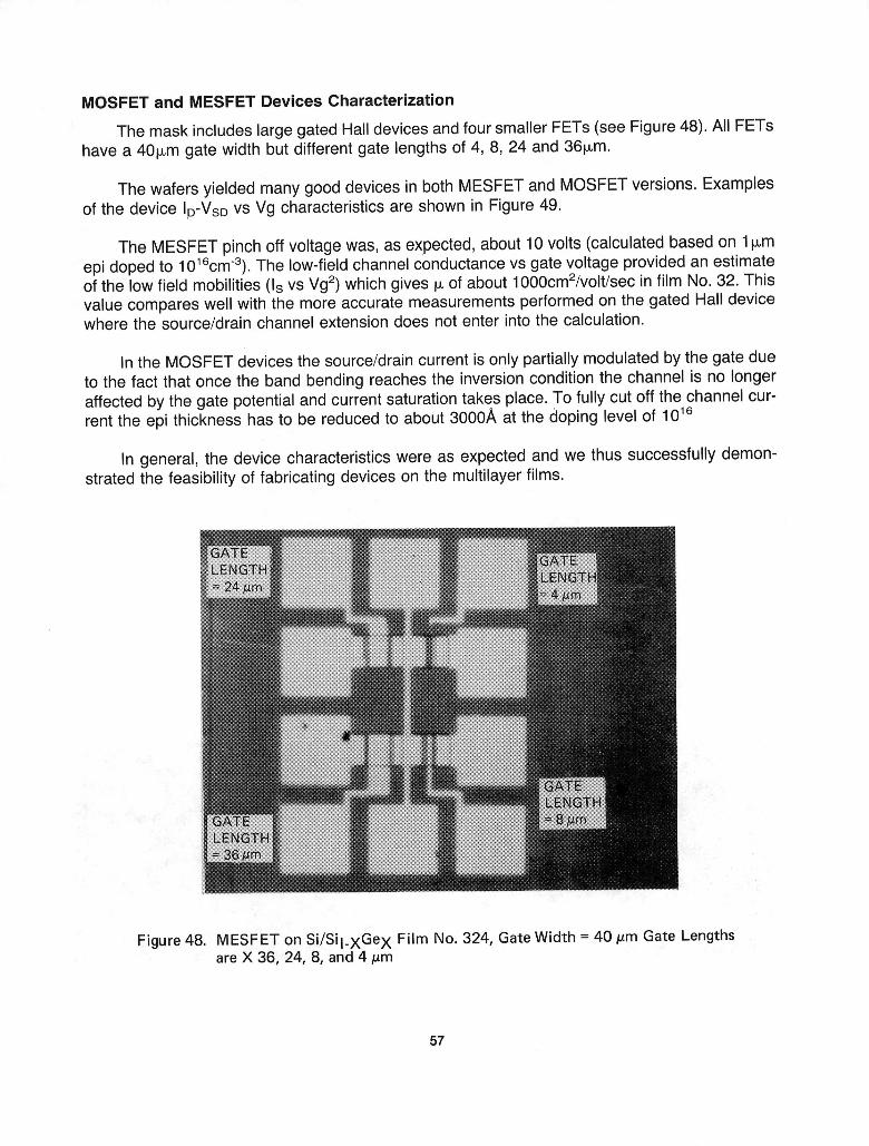
MOSFETand MESFETDevicesCharacterization
ThemaskincludeslargegatedHalldevicesandfoursmallerFETs(seeFigure48).AllFETshavea 40_m gatewidthbutdifferentgate lengthsof 4, 8, 24 and361_m.
ThewafersyieldedmanygooddevicesinbothMESFETandMOSFETversions.Examplesof thedeviceID-VsDVSVgcharacteristicsareshowninFigure49.
TheMESFETpinchoffvoltagewas,as expected,about10volts(calculatedbasedon1_mepidopedto 1016cm3).Thelow-fieldchannelconductancevsgatevoltageprovidedanestimateofthelowfieldmobilities(IsvsVg2)whichgivesi_ofabout1000cm2/volt/secinfilmNo.32.ThisvaluecompareswellwiththemoreaccuratemeasurementsperformedonthegatedHalldevicewherethesource/drainchannelextensiondoesnotenterintothecalculation.
IntheMOSFETdevicesthesource/draincurrentisonlypartiallymodulatedbythegateduetothe factthatoncethe bandbendingreachesthe inversionconditionthe channelis nolongeraffectedbythegatepotentialandcurrentsaturationtakesplace.To fullycutoff thechannelcur-rentthe epithicknesshasto be reducedto about3000Aatthedopinglevelof 10le
Ingeneral,the devicecharacteristicswereas expectedandwe thussuccessfullydemon-stratedthe feasibilityof fabricatingdevicesonthe multilayerfilms.
Figure 48. MESFET on Si/SiI_xGe x Film No. 324, Gate Width = 40/_m Gate Lengthsare X 36, 24, 8, and 4 #m
57

(a) No. 324 (b) No. 335
ID-VsD; Vg FOR MESFET ON Si/SiGe
-C-
(c) ID-VsD; Vg FOR MESFET ON Si No. 315
(d) DEVICE314 (Si) (e) DEVICE342 (Si/SiGe)
Figure 49. ID-VSD; Vg of MOSFET Devices
58

Summary
1. Thin silicon dioxide films were thermallygrown on multilayerfilms usingthe uppermostSilayer. The oxide and its interfacewith the semiconductor(Si) seem to be the same as thaton bulk Si.
2. Thermal oxide grown on multilayer films on which alloy layers are consumed shows noGe content to within =1% sensitivity. Ge pile-up at the oxide/semiconductor interfacewas detected.
3. MOSFET and MESFETdevices were successfully fabricated on multilayer Si/SiGe films.Device performance characteristics were consistent with the measured multilayer filmmaterial parameters.
59


SECTION VI
DISCUSSION AND CONCLUSION
It is now worthwhile to summarize the most prominant features of the multilayer films.
1. Hall effect measurements of the films show the electron Hall mobility in multilayer films tobe up to 50 percent higher than that of single layer of Si or SiGe alloy films of comparabletotal thickness and carrier density.
2. The enhanced mobility was observed for carrier density between 0.8 x 10¹⁶and 2 x 1017cm"3,in (100) oriented films but not on (111) films.
3. Carrier non-freezout occurs in the multilayer films at low temperature. Carrier densitydecreased by only a factor of 3 or 4 from 300°K to 20°K.
4. The mismatch in the lattice constants of the alloy and the Si layers is to a large extentaccommodated in the multilayer films through elastic strain. The strain relief (e.g.,through dislocations) in the multilayer and very thin films (e.g., 500A) is considerablysmaller than in thick alloy films (e.g, >1 i_m).
5. The electron density (n) and Hall and drift mobilities (p,H,l_)are strongly modulated withdepth, with the modulation period equal to the superlattice period. The peaks of n, pH,and p,almost coincide and occur at the SiGe on Si interfaces of the film. The modulationof n, pH, and I_ increases sharply at lower temperature with the profile of n becoming5-function-like at very low temperature.
The above experimental observations lead us to consider two distinctive mechanisms toaccount for the temperature dependence of the carrier distribution. The first is a dopant segrega-tion model in which the dopant atoms are assumed to segregate to the interfaces during the filmgrowth. This is assumed to happen as a result of gettering of the impurity atoms by the crystallineimperfections at the interfaces which are generated due to the mismatch between the two materi-als. The temperature dependence of the carrier profile can be accounted for as follows: At roomtemperature, thermal diffusion causes the broadening of the electron distribution with a character-istic length equal to the Debye length D=400A for N = 1016cm "3.At lower temperatures the elec-tron distribution becomes less diffused and eventually at very low temperature it approaches thatof the impuritydistribution. The non-freezout is assumedto occur because the actual dopant con-centration is much larger than the average value; possibly as high as 1018cm3 where the dopantactivation energy is very small.
The second mechanism considered is electron transfer across the heterojunction due to thediscontinuity (AEc)in the conduction band as illustrated in Figure 50. Electrons transfer from thehigher conduction band side to the lower conduction band side (assuming as in our case the twosides are n-doped). Band bending occurs due to the resultant electric field. With small AEc, theelectron distribution is fairly broad due to thermal diffusion but becomes sharper as the tempera-ture is lowered. Carrier non-freezout should occur only if ,_Ecis larger than the activation energyof dopants in the higher conduction band side of the junction. The activation energy for phospho-rus in Si is about 45 mV and thus the value of _Ec in the heterojunction should be larger than thatto account for the non-freezout.
61

ACCUMULATION DEPLETIONLAYER
FERMI LEVEL
l n-TYPE n-TYPE
LLIz VLU SiGe
°IuJ
DISTANCE _ _ VALENCE BAND"r" Si
Figure50. IdealEnergyBandDiagramof SiGe/Si Heterojunction
The question now is how do the two models account for the enhanced mobility and the mobil-ity profile. In the dopant segregation model, the scattering due to ionizeddopants in the bulk of thelayers is expected to be less than that in an otherwise homogeneous semiconductor with thesame average dopant density. This might result in higher average mobility, but the mobilityshouldhave its minimum value near the peak of N; the reverse of what we saw in our films. In the electrontransfer model, the separation of electrons from their parent dopant atoms should result in lessscattering and thus higher mobility in the lower conduction band side of the heterojunction. This isconsistent with the coincidence of the peaks of _ and n.
Remaining to be determined, however, is the electronic structure of the heterojunctionbetween the Si and SiGe layers. An ideal heterojunction structure is shown in Figure 50. It isbased on the assumption of the absence of interface states in the band gap. The value of _Ec(30mV) is obtained by assuming it is linearly proportional to the Ge content (-15 percent) andthus is equal to 0.15 _Ec (Si/Ge) where AEo(Si/Ge)= .18eV is the conduction band discontinuityin the Si/Ge heterojunction (Ref 16). It should be noted that this value of AEc (Si/Ge) is deducedfrom the difference between the electron affinities of the two semiconductors and not from directmeasurement.
The generation of interface states due to lattice imperfections can cause considerable com-plications in the electronic structure of the heterojunction. For example, in n-n heterojunctions theoccurrence of acceptor type interface states in the band gap will result in an energy barrier at theheterojunction as shown in Figure 51 due to the formation of depletion layers on both sides of thejunction. Other effects such as elastic strain can cause significant changes in the band structure.For example, the uniaxial strain in the (001) direction of 0.3 percent found in our films shouldresult in the splitting of the lowest conduction band valleys - (001) relative to (100) and (010) - byabout 25 meVdetermined from the deformation potential of Siwhich is -8.6V (Ref 17).The redis-tribution of electrons amongst these valleys is the major contributor to piezoresistance effect inn-type Si and Ge (Ref 18). Experimental determination of the electronic structure of theheterojunction is, however, necessary for better understanding of the problem.
62

DEPLETION LAYERS
€ ¢ ¢ 0 ® ® ® ® ®0 FERMI LEVEL®
INTERFACE STATES
> ®n-
Z
O_
DISTANCE
Figure 51. EnergyBand Diagramof SiGe/SiHeterojunction with InterfaceStates
Now, let us discuss the potential device application of the multilayer films. An importantquestion is how high a mobility can be expected in these films. Mobility enhancement occurs dueto several mechanisms including reduction of the scattering by separation of electrons from ion-ized dopants and piezoresistance effects due to tensile strain which causes the splitting of theconduction band valleys as mentioned above. Another related mechanism is the splitting of theconduction band valleys by the confinement of the electrons in narrow energy wells. This mecha-nism has been studied extensively in conjunctionwith the inversion layers in MOS devices (Ref 4,17 and 19), and by Professor J. Moriarty of Cincinnati University in SiGe/Si superlattice (Ref 5).Electron confinement is known to occur in heterojunctions such as the GaAs/GaAIAssystem andpossibly occurs in our films. Unlike GaAs where the lowest valley of the conduction band is cen-tered at the origin of the Brillouin zone, the Si valleys are located along the (100) direction and itsequivalents. The quantization of the electron motion perpendicular to the plane of the film resultsin splitting of the energy bands into several sub-bands. The lowest sub-band corresponds to the(001) valley due to the fact that the largest effective mass is associated with that direction (seeFigure 52). The energy difference between the sub-band and the next one is a function of theshape and depth of the well. If electrons occupy only the lowest sub-band, then their motion is twodimensional in nature and their effective mass is only 0.194 mo;the transverse mass of the ellip-soidal valleys of the Si conduction band. This is a factor of 1.4 smaller than the effective mass inbulk Si.
63

E100t/ EOOl
_3 Si SiGe
LI.! _z ow _
w
DISTANCE_ -r_IFigure 52. Hypothetical EnergyBandDiagramof the Si/Sil.x Gex Heterojunction
The first mechanism, namely, the separation of electrons from the ionized donors, brings themobility to the value determined by phonon scattering, i.e., the mobility of lightly doped bulk semi-conductor. For example, in the heterostructure of GaAs/GaAIAs the mobility obtained at roomtemperature is 8000 cmT/volt/secwhich is the same as that of lightly doped GaAs. The mobilityenhancement, however, is much larger at lower temperature where the ionized dopant scattering,usually the dominant mechanism at low temperature, is virtually absent. The electron mobility inlightly doped n-type Si is --1500 cm2/volt.sec.
The second and third mechanism, the elastic strain (piezoresistance) and electron confine-ment both cause the splitting of the conduction band valleys. Their effect is additive only if theelectron redistribution amongst the valleys is not complete. In the limiting case where electronsoccupy only the lowest valley, the enhancement factor is 1.4; the ratio of the 2-d effective massrelative to the bulk effective mass. Thus, the expected electron mobility in an ideal heterostructuredevice, described in the next paragraph, can reach -2,100 cm2/volt.sec. In bulk MESFETdevices with carrier concentrations of _1017cm-3 the mobility is about 800 cm2/volt-sec. Inenhancement-type MOSFET devices the channel mobility is -700 cm2/volt/sec.
An ideal film structure should be such that the lower band semiconductor m presumablySiGe -- is undoped. The dopants should be incorporated in the higher band semiconductor pref-erably some distance away from the interface to minimize ionized impurity scattering. The thick-ness of the dopant layer should be such that it is completely depleted due to electron transferacross the heterojunction. Such film requirements might only be feasible in MBE grown filmswhere low growth temperature minimizes dopant diffusion and where more precise control oflayer thickness can be achieved. A set of film parameters suitable for use in MESFET devices is:
64

average carrier density _1017, total film thickness of about 2500A, and layer thickness deter-mined by the depletion requirement and AEc. For AEc --50 mV the optimum layer thickness isabout _2000A. The gate voltage required for fully depleting the channel is about 5 volts. Deple-tion type MOSFETS can be fabricated on films of similar parameters but of only about 1000Athickness.
Suggestion for Future Studies
The experimental evidence obtained so far indicates strongly the occurrence of electron con-finement at the heterojunctions. This mechanism can lead, as seen in the work of Moriarty (Ref5)and others (Ref 4), to significant transverse mobility enhancement. It is thus of paramount impor-tance to investigate the nature of this confinement. An immediate area of concern is the investiga-tion of the electronic structure of the heterojunction between Si and SiGe layers. Another area isthe transport properties at very low temperatures. For example, magnetoresistance experimentsshould be performed to search for Schubnikov-de Haas oscillation as evidence of electron con-finement (2-dimensional electron gas).
65


SECTION VII
ABBREVATIONS AND SYMBOLS
(100), (010), (001), (111) m Miller indices of crystal planes
A m Angstrom units (10"1°Meters)
AES -- Auger Electron Spectroscopy
A1 m Aluminum
Aum Gold
B2H6- Diborane
Bz _ Magnetic field intensity in "depth" direction of gated Hall Device
C -- Capacitance
CF4_ Carbon tetrafluoride
ccpm _ cubic centimeters per minute
cm -- centimeters
cm 3 -- per cubic centimeter
cm2/volt/sec_ square centimeters per volt per second (unit of mobility)
CVD -- Chemical Vapor Deposition
Cr m chromium
D- Debye length
Ex m Electrical field component along length of gated Hall device
Ey- Electrical field component along width of gated Hal device
EBMF _ Electron Beam Micro-Fabricator
EDXS -- Energy Dispersive X-ray Spectroscopy
FET _ Field Effect Transistor
G -- Channel conductance
GHD _ Gated Hall Device
GaAs _ Gallium arsenide
GaA£As -- Gallium aluminum arsenide
Ge -- Germanium
GeH4 _ Germane
H2- Hydrogen
He _ Helium
HC1 -- Hydrogen chloride
HF _ Hydrogen fluoride
67
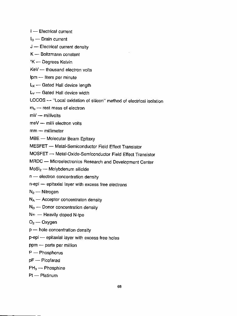
I-- Electrical current
ID -- Drain current
J -- Electrical current density
K- Boltzmann constant
°K _ Degrees Kelvin
KeV -- thousand electron volts
Ipm _ liters per minute
Lx _ Gated Hall device length
Ly- Gated Hall device width
LOCOS _ "Local oxidation of silicon" method of electrical isolation
mo-- rest mass of electron
mV- millivolts
meV- milli electron volts
mm _ millimeter
MBE _ Molecular Beam Epitaxy
MESFET _ Metal-Semiconductor Field Effect Transistor
MOSFET _ Metal-Oxide-Semiconductor Field Effect Transistor
MRDC _ Microelectronics Research and Development Center
MoSi2_ Molybdenum silicide
n -- electron concentration density
n-epi _ epitaxial layer with excess free electrons
N2_ Nitrogen
NA -- Acceptor concentraton density
ND--Donor concentration density
N+ -- Heavily doped N-tpe
02 _ Oxygen
p _ hole concentration density
p-epi -- epitaxial layer with excess free holes
ppm _ parts per million
P -- Phosphorus
pF _ Picofarad
PH3_ Phosphine
Pt _ Platinum
68

PtSi2- Platinum silicide
q m charge
RBS m Rutherford Backscattering Spectroscopy
aN -- Hall Factor
rpm -- revolutions per minute
S _ Seconds
SEM _ Scanning Electron Microscope
SIMS -- Secondary Ion Mass spectrometry
Si- Silicon
SiGe -- Silicon-germanium Alloy
Si/SiGe -- Silicon on silicon-germanium alloy
SiC w Silicon carbide
SiGe/Si -- Silicon-germanium alloy on silicon
SiH2CI2 _ Dichlorosilane
Sill4 _ Silane
Si02 _ Silicon dioxide
T m Temperature (degrees Kelvin)
TEM- Transmission Electron Microscopy
V -- Volts
Vso_ Source-drain voltage
Vg w Gate voltage
W- Depletion width of gated Hall device
u _ mobility
UHb Hall mobility
um _ microns or micrometers (10.6 meters)
x _ length
y _ width t directions on gated hall devicez -- depth
69


SECTION VIII
REFERENCES
1. L. Esaki and R. Tsu: "Superlattice and Negative Differential Conductivity in Semiconduct-ors," IBM J. Res. Develop. 14, p. 61 (1970).
2. R. Dingle, H. L. Stormer, A. C. Gossard and W. Wiegmann: "Electron Mobilities inModulation-Doped Semiconductor Heterojunction Superlattices," Appl. Phys. Lett. 33, p.665, (1978).
3. L. Stomer, R. Dingle, A. C. Gossard, W. Wiegmann, and M. D. Sturge: "Two-DimensionalElctron Gas at a Semiconductor-Semiconductor Interface," Solid State Comm. 19, p. 705(1979).
4. J.J. Quinn and P. J. Stiles, "Proceedings of the InternationalConference on Electronic Prop-erties of Quasi-Two-Dimensional Systems", Surface Science 58, No. 1, p.1 (1976).
5. J.A. Moriarty and S. Krishnamurthy:"Theory of Silicon Superlattice Electronic Structure andEnhanced Mobility," J. Appl. Phys. 54. p. 1892 (1983).
6. P.J. Stiles: "The Artificial Superlattice in a Two-Dimensional System," Science 73, p. 252(1978).
7. J. Oda: "Vapor Growth of Silicon-Germanium Crystals," Japan J. Appl. Phys. 1, p. 131(1962).
8. K.J. Miller and J. J. Grieco: "Epitaxial Silicon-GermaniumAlloy Films on Silicon Substrates,"J. Electrochem. Soc. 109, p. 70 (1962).
9. L. I. Halberg and J. H. Nevin: "Silicon Germanium Alloy Growth Control andCharacterizaton," J. Electron. Mat, 11, p. 779 (1982).
10. H. Ahroni, A. Bar-Lev, I. P. Blech, and S. Margalit: "Epitaxial Growth of Silicon-GermaniumSingle Crystals," Thin Solid Films 11, p. 313 (1972)
11. G. M. Oleszek and R. L. Anderson, "Hetroepitaxial Growth of SixGel.×Alloys by ThermalDecomposition of SiH3GeH4,"J. Electrochem. Soc. 120, p. 554 (1973).
12. V.A. Tolomasov, T. A. Zeveke, L. I. Kornev, and N. V. Gudkova: "Growth of HeteroepitaxialSi-Ge Solid-Solution Films from Hybrids," Sov. Phys. Crystallogr. 20, p. 660 (1975).
13. J. H. Van der Merwe: "Crystal Interfaces. Part I. Semi-Infinite Crystals," Appl. Phys. 34. p.117 (1963). See also references in paer by G. C. Osborn et. al. Appl. Phys. Lett. 41, p. 172(1982).
14. P. L. Gourley and R. M. Biefeld: "Ga (As,P) Strained-Layer Superlattices: A ternary Semi-conductor with Independently Adjustable Band Gap and Lattice Constant, " J. Vac. Sci. 4Technology Second Series Vol. 1, p. 383, (1983).
15. S. Margalit, A. Bar-Lev, A. B. Kuper and H. Aharoni, and A. Neugroschel: "Oxidation ofSilicon-Germanium Alloys," J. Crystal Growth, 17, p. 288 (1972).
16. A. G. Milnes and H. Veucht: "Heterojuntions band Metal-Semiconductor Junctions," pp.98-99, Academic Press (1972).
71

17. I. Eisele, H. Gersch, and G. Dorda: "Effective Masses in (100) Silicon Inversion Layers,"Solid State Comm. Vol. 22, p. 185 (1977).
18. C. S. Smith: " Piezoresistance Effect in Germanium and Silicon," Phys. Rev. Vol. 94, p. 42(1954).
19. A.B. Fowler, F. F. Fang, W. E. Howard, and P. J. Stiles: "Oscillatory Magnetoconductance inSi Surfaces," Proc. of Inst. Conf. Semiconductors, Kyoto, 1966, pp. 331-335.
72


1. Report No. 2. Government Accession No. 3. Recipient's Catalog No.NASACR-3903
4. Title and Subtitle 5. Report DateJune 1985
INVESTIGATION OF SUPERLATTICE DEVICE STRUCTURES 61 Performing Organization Code
7. Author(s) Isoris S. Gergis, Harold M. Manasevit, Alice L. Lin, and 8. Performing Organization Report NoA. Brooke Jones
10. Work Unit No.9. Performing Organization Name and Address
Rockwell International CorporationMicroelectronics Research and Development Center 11. Contract or Grant No.3370 Miraloma Ave. NASI-16102Anaheim, CA 92803
12. Sponsoring Agency Name and Address J' 13. Type of Report and Period Covered
National Aeronautics and Space Administration Contractor ReportWashington, D,C. 20546 14, Sponsoring Agency Code
506-54-13-12
15. Supplementary NotesLangley Technical Monitors: A.L. Fripp and R. L StermerFinal Report
16. Abstract
This report describes the investigationof the growth, properties, and the structure of epitaxial multilayerSi/Sil.xGexfilms grownon bulk Silicon Substrates. It also describes the fabrication and characterization of MOSFET and MESFET devices made on theseepitaxial films.
Films were grown in a CVD reactor using hydrides of Si and Ge with H2 and He as carrier gases. Growth temperatures werebetween 900°C andd 1050°C with most films grown at 1000°C.Layer thickness was between 300A and 2000A and total film thicknesswas between 0.25p.m and 71_m.The Ge content (X) in the alloy layers was between .05 and 0.2.
N-type multi{ayerfilms grown on (100) p-type Si showed Hall mobility in the range 1000 to 1500cm2Nsec for an average carrierconcentration of - 1 x 10TM cm3. This is up to 50% higher than the Hall mobility observed in epitaxial Si films grown under the samecon-ditionsand with the same average carrier concentration. The mobility enhancement occured in films with averagecarrier concentration (n)from 0.7 x 10¹⁶to 2 x 1017cm3, and total film thickness greater than 1.0p.m.No mobility enhancement was seen in n-type multilayerfilms grown on (111) Si or in p-type multilayer films.
The structure of the films was investigated was using SEM, TEM, AES, SIMS,and X-ray double crystaldiffraction techniques. Thefilm compositionprofile (AES,SIMS) showedthat the transition regionbetween layers isof the order of about IOOA.The TEM examinationrevealed a well defined layeredstructure with fairly sharp interfaces and good crystaline quality. It alsoshowed that the first few layers ofthe film (closest to the substrate) are uneven, most probably due to the initial growth pattern of the epitaxialfilm wheregrowth occurs firstin isolated islannds that eventually grow and coalesce. The X-ray diffraction measurement determined the elastic strainand strain reliefinthe alloy layers of the film and the elastic strain inthe interveningSi layers. The strain relief in thick alloy layers was found to be considera-bly larger than that in thin alloy layers, indicating that the mismatch between the lattice parameters of the alloy and Si is accommodatedmostly by elastic strain in thin layers. The elastic strain in the Si/xGe.and the Si layers are -0.3% and + .2% respectively. Measurementof the carrier density and HallMobility as a function of temperature showedthat the carriers do not completely freeze-out at very low tem-peratures (_<50°K).The measurement of the carrier concentration profile (C-V measurement)within the film showed very strong periodicvariationofwith depth. The peaks of n are coincident with the SiGe-on-Si interfaces. Hall and drift mobility profiles were also strongly mod-ulated with their peaks almost coincident with those of n. The modulation of n and the mobility increase with decreasing temperature.
The above results indicate electron confinement might be occurring at the layer interfaces of the multilayerfilms. Themechanismof electron confinement is not clear at this time. Factors that probably play important roles are the conduction band discontinuity at theheterojunction and the elastic strain in the SiGe and Si layers.
17. Key Words iSuggested by Author(s)) 18. Distribution StatementSuperlatticeSilicon Uqclassified -- UnlimitedMobility EnhancementSi/SiGe Heterostructure
Subject Category -- 33
19. Security Classif. (of this report) 20. Security Classif. (of this page) 21. No. of Pages 22. Price
UNCLASSIFIED UNCLASSIFIED 80 A05,i
i
For sale by the National Technical Information Service, Springfield, Virginia 22161NASA-Langley, 1985


National Aeronautics and THIRD-CLASS BULK RATE Postageand Fees Paid
SpaceAdministration National Aeronautics and I._ ISpace Administration
Washington, D.C. NASA45120546
Official Business
Penalty for Private Use, $300
_A POSTMASTER: If Undeliverable (Section 158Postal Manual) Do Not Return