of nanoparticle superlattice thin films
TRANSCRIPT
1
Growthmodesofnanoparticlesuperlatticethinfilms D. Mishra1, D. Greving1, G. A. Badini Confalonieri1,2, J. Perlich3, B.P. Toperverg1, H. Zabel1, and O. Petracic1,4 1 Institute for Experimental Condensed Matter Physics, Ruhr-University Bochum, D-44780 Bochum, Germany 2 Instituto de Ciencia de Materiales, E-28049 CSIC Madrid, Spain 3 Deutsches Elektronen-Synchrotron DESY, D-22607 Hamburg, Germany 4 Juelich Centre for Neutron Science JCNS-2 and Peter Gruenberg Institute PGI-4, Forschungszentrum Juelich
GmbH, 52425 Juelich, Germany
Abstract: We report about the fabrication and characterization of nanoparticle thin film
superlattices, which show two of the three thin film growth modes, i.e. Volmer-Weber and
Frank van der Merwe growth. In addition three-dimensional mesocrystallite growth is
evidenced. The formation into different systems is accomplished by tuning the particle-to-
substrate interaction. The understanding of the mechanisms ruling nanoparticle self-assembly
represents an important step toward the fabrication of novel materials with tailored optical,
magnetic or electrical transport properties.
The advent of controlled thin film growth about seven decades ago revolutionized many areas
of science and technology1-6. Examples are optical coatings1,2 , magnetic layers and
multilayers3,4 or semiconductor thin films5,6. Thin films enabled the development of
important applications and lead to the discovery of novel effects which arise from the
structure of materials and the presence of surfaces7,8 or interfaces between different layers9,10.
In the early stage of research on thin films it soon became clear that it was imperative to
understand the mechanisms which control and define the growth of thin films to achieve good
control over these novel materials. Hence the huge effort of the scientific community to
characterize, optimize and understand film growth. Evidently thin films are composed of
atoms, which are their zero-dimensional building blocks. Extending this concept,
nanoparticles (also termed 'nanocrystals') can also serve as zero-dimensional building blocks

2
which by self-assembly may form two-dimensional thin films or three-dimensional crystals
(so-called 'nanoparticle superlattices'), analogous to atomic films and crystal
lattices11,12,13,14,15,16,17,18,19,20,21. Atomic thin film growth is understood to occur in form of
three basic growth modes, which result from competing energy terms during the film
deposition, i.e. Frank van der Merwe, Stranski-Krastanov, and Volmer-Weber growth8,22,23.
Various processes occur when atoms arrive at a substrate during thin film growth. That is
adsorption, desorption, diffusion, finding or leaving of equilibrium positions. These processes
occur simultaneously averaged over the ensemble of arriving atoms. Consequently, textbooks
describe these processes in the framework of macroscopic thermodynamics8,22,23.
An important quantity, e.g., is the equilibrium vapor pressure pe of atoms, being defined as the
pressure, where condensation and evaporation of atoms at the substrate surface occurs at the
same rate. Thin film growth is possible, when the pressure of the vapor near the substrate, p,
is larger than the equilibrium vapor pressure pe. In the case of a supersaturated vapor, a free
energy difference exists between the vapor and the condensed atoms in the film.
Consequently a chemical potential exists, which is responsible for further condensation of
atoms into the film23. This concept can also be transferred to nanoparticle (NP) films and
superlattices. While NPs are in the solvent, the solvent constitutes the confining volume.
Upon evaporation of the solvent the volume shrinks and leads to an increase of the NP 'vapor'
pressure. Eventually NP film growth is possible.
As in the case of atoms, the interplay of various free energy terms determines the way on how
the NP films will grow. These are in detail23: an entropic contribution ETS, an inter-particle
energy term Ep, summing up all relevant types of interactions between NPs24, and a NP-to-
substrate interaction energy, Es. A further important factor is the diffusion energy barrier, Ed,
which can be overcome by 'thermal' energy kBTs. Hereby Ts is a quantity comparable to a
substrate 'temperature', which precise physical meaning still needs to be understood for NP

3
systems. Depending on the relative magnitudes of Ed and kBTs the NPs will either stay fixed at
one place once they are attached to the substrate or move freely to seek energetically more
favorable locations considering the two extreme cases.
From a comparison of these free energy terms one finds22,23 that three different growth modes
follow: in the case where NP-to-substrate energy, Es, dominates a layer-by-layer growth is
found, viz. the so-called Frank-van-der-Merwe growth mode (FvdM). This case is depicted in
Fig. 1. Once a stable cluster (or 'nucleus') of NPs is formed, the following NPs prefer to attach
at the periphery of the nucleus in contact with the substrate. Accordingly this leads to the
advancement of planar film growth23. Depending on the ratio of Ed and kBTs (i.e. the mobility
of NPs) one will either obtain polycrystalline or single-crystalline superlattices. In the first
case, the immobility of NPs leads to the nucleation of many independent superlattice
crystallites, while, in the other case, the large mobility enables the NPs to seek equilibrium
positions and hence promotes single-crystal growth.
Figure 1: Schematic representation of the three known film growth modes23. The spheres can
be either atoms or NPs. When NPs approach a substrate, either adsorption, desorption or
diffusion occurs. Depending on the free energy contributions one finds Frank-van-der-Merwe
(FvdM), Volmer-Weber (VW), or Stranski-Krastanov (SK) growth.
If, however, the NP-NP energy dominates, the NPs tend to attach on top of existing NPs and
hence favor three-dimensional or island growth (Fig. 1). This mode is termed Volmer-Weber

4
growth (VW). Whether polycrystalline or single-crystalline islands arise also depends on the
mobility as in the FvdM case.
The third growth mode constitutes in some sense a mixed situation, where layered and island
growth coexist. It can be understood by a change of growth mode during self-assembly. As
the first layer experiences a large interaction to the substrate the growth starts in a planar
fashion. Once the substrate is covered by a monolayer of particles the ratio of interaction
energies changes so that island growth is preferred. This mode is termed Stranski-Krastanov
mode (SK) and is shown schematically in Fig. 1.
An alternative approach toward the distinction of growth modes is based on the analysis of
'surface tension' energies. By comparing various surface tension contribution one basically
arrives at the same distinction of three basic growth modes23.
The aim of the present article is to explore thin films and superlattices composed of iron oxide
NPs. By varying the particle – substrate interaction energy we obtain two of the three growth
modes in analogy to atomic thin films, viz. FvdM and VW growth. In addition we obtain
three-dimensional growth comparable to seed-mediated bulk crystal growth. These growth
modes are verified through a series of case studies reported in this article. The third film
growth mode, SK growth, still evades experimental realization. Moreover, as increasingly
revealed by other studies,25 it turns out that the influence of the drying solvent plays a
considerable additional role in the formation of NP superlattice films.
The first case to be considered is a monolayer thin film of NPs, spin-coated onto a Si
substrate (sample 'Si'), the scanning electron microscopy (SEM) image of which is shown in
Figure 2a. A complete monolayer of NPs is clearly visible, covering the entire substrate
surface. The NPs self-assemble into a 2D hexagonal lattice, showing domain boundaries,
vacancies and other structural defects analogous to those found in polycrystalline solids.
Moreover, in some places it is possible to observe an incomplete second layer forming a

5
system of effectively 1.2 to 1.5 monolayers. The growth mode of this film clearly resembles
that of layer-by-layer or FvdM growth.
Figure 2: SEM images of NPs spin-coated on (a) silicon substrate with native oxide (sample
'Si') (b) PMMA coated silicon (sample 'PMMA_ 4P') showing a completely different NP
arrangement on the substrates. The corresponding GISAXS patterns are shown in (c) and (d)
respectively.
Although SEM imaging provides us with a useful visual inspection of the sample, it alone is
insufficient to address a comprehensive study of long-range correlations of NPs across the
substrate. A more powerful characterization technique is needed, providing information on
both the in-plane as well as the in-depth structural ordering. These requirements are met by
the use of Grazing Incidence Small Angle X-ray Scattering (GISAXS), a surface sensitive x-
ray scattering technique which provides electron density profiles statistically averaged over a

6
large lateral area. By the glancing incident and exit angles of the x-ray beams the surface
sensitivity is enhanced26.
The corresponding GISAXS pattern of NPs on Si, measured at an incident angle (αi) of 0.5º,
is shown in Figure 2c, with the intensity plotted on a logarithmic scale coded in color scale
shown on the right hand side. Two distinct features can be observed in the scattering pattern.
In first place, the intensity is distributed in ring like patterns (although not continuous). At
least three such rings can be seen in this pattern. Secondly, on top of the rings high intensity
peaks, which modulate the ring intensity, can be observed. The peaks are extended along qy
and qz directions and appear symmetrically on both sides of the qz axis along the ±qy axis.
These features represent the Fourier transform of the in- and out-of-plane electron density
variations, which basically depend on two factors: the morphology (shape and size) of the
NPs and the particle-particle correlations (NP ordering). The ring like pattern is a
manifestation of the Fourier transform of the morphology, i.e. the form factor of the spherical
NPs. Simultaneously, the intense Bragg peaks seen as streaks extending in the qz direction are
manifestations of the scattering function, the Fourier transform of the particle-particle
correlation function and hence indicate the presence of long-range ordering of the NPs. In
other words, the high intensity Bragg peaks arise from long-range NP ordering in the
GISAXS geometry, where the momentum transfer vector or the scattering vector (Q) is of the
order of the reciprocal lattice vector (~G) of the NP in-plane lattice. The Bragg peaks are an
indication of the crystal structure and can be used to determine the NP unit cell structure since
in small angle geometry the |Q|-1 correspond to few tens of nm, which is similar to the inter-
particle distances for the NPs used in this study. The pattern shown in Figure 2c can therefore
be assigned to a hexagonal close packed (HCP) lattice of lattice constant 20.38 nm, which is
larger than the NPs average diameter of 18 nm as found from SEM images. The discrepancy
can be explained by the fact that the SEM image is less sensitive to the organic oleic acid
shell, because the element contrast in SEM scales with the atomic number of the elements.
7
Consequently, the SEM will rather reveal the diameter of the individual iron oxide NPs, while
GISAXS probes correlation lengths, i.e. periodicities and hence the distances between NPs
including the organic shells.
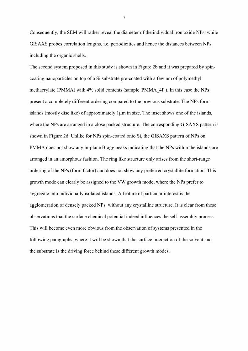
The second system proposed in this study is shown in Figure 2b and it was prepared by spin-
coating nanoparticles on top of a Si substrate pre-coated with a few nm of polymethyl
methacrylate (PMMA) with 4% solid contents (sample 'PMMA_4P'). In this case the NPs
present a completely different ordering compared to the previous substrate. The NPs form
islands (mostly disc like) of approximately 1μm in size. The inset shows one of the islands,
where the NPs are arranged in a close packed structure. The corresponding GISAXS pattern is
shown in Figure 2d. Unlike for NPs spin-coated onto Si, the GISAXS pattern of NPs on
PMMA does not show any in-plane Bragg peaks indicating that the NPs within the islands are
arranged in an amorphous fashion. The ring like structure only arises from the short-range
ordering of the NPs (form factor) and does not show any preferred crystallite formation. This
growth mode can clearly be assigned to the VW growth mode, where the NPs prefer to
aggregate into individually isolated islands. A feature of particular interest is the
agglomeration of densely packed NPs without any crystalline structure. It is clear from these
observations that the surface chemical potential indeed influences the self-assembly process.
This will become even more obvious from the observation of systems presented in the
following paragraphs, where it will be shown that the surface interaction of the solvent and
the substrate is the driving force behind these different growth modes.

8
Figure 3: SEM images of NPs spin-coated on (a) PMMA/MA 33% coated silicon (sample
'PMMA_33P') (b) silicon with 300 nm of silicon oxide substrate (sample 'SiO2'). The
corresponding GISAXS patterns are shown in (c) and (d) respectively.
In the following we consider two systems composed of NPs spin-coated on Si pre-coated with
copolymer polymethyl methacrylate/ methacrylic acid (PMMA/MA) with 33 % solid contents
(sample 'PMMA_33P') and on Si substrates with 300 nm of thermal SiO2, shown in Figure 3a
and 3b, respectively.
The use of a PMMA/MA that differs in composition from the one considered in the previous
section brings forward important changes in the self-assembly process. The NPs on
PMMA/MA 33% substrates form islands partially interconnected with each other to create a
meander like pattern.
The inset in Figure 3a shows a magnified view of one of the islands, composed of several
layers of NPs. Remarkably, the NP layers form terraces, which have preferred orientations of
crystalline order, although the orientations of the crystallites inside the terraces are different
9
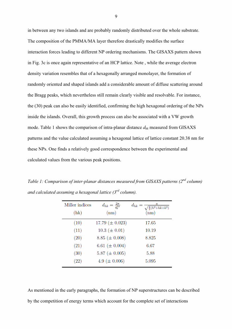
in between any two islands and are probably randomly distributed over the whole substrate.
The composition of the PMMA/MA layer therefore drastically modifies the surface
interaction forces leading to different NP ordering mechanisms. The GISAXS pattern shown
in Fig. 3c is once again representative of an HCP lattice. Note , while the average electron
density variation resembles that of a hexagonally arranged monolayer, the formation of
randomly oriented and shaped islands add a considerable amount of diffuse scattering around
the Bragg peaks, which nevertheless still remain clearly visible and resolvable. For instance,
the (30) peak can also be easily identified, confirming the high hexagonal ordering of the NPs
inside the islands. Overall, this growth process can also be associated with a VW growth
mode. Table 1 shows the comparison of intra-planar distance dhk measured from GISAXS
patterns and the value calculated assuming a hexagonal lattice of lattice constant 20.38 nm for
these NPs. One finds a relatively good correspondence between the experimental and
calculated values from the various peak positions.
Table 1: Comparison of inter-planar distances measured from GISAXS patterns (2nd column)
and calculated assuming a hexagonal lattice (3rd column).
As mentioned in the early paragraphs, the formation of NP superstructures can be described
by the competition of energy terms which account for the complete set of interactions
10
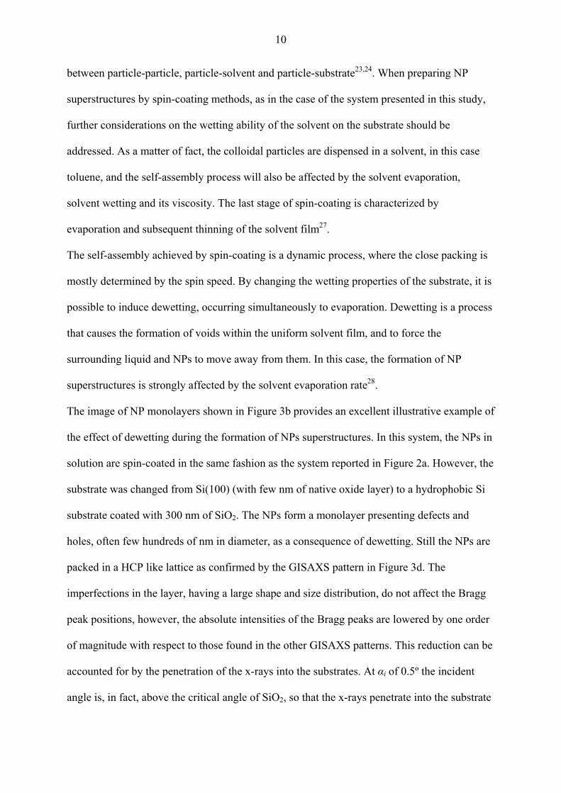
between particle-particle, particle-solvent and particle-substrate23,24. When preparing NP
superstructures by spin-coating methods, as in the case of the system presented in this study,
further considerations on the wetting ability of the solvent on the substrate should be
addressed. As a matter of fact, the colloidal particles are dispensed in a solvent, in this case
toluene, and the self-assembly process will also be affected by the solvent evaporation,
solvent wetting and its viscosity. The last stage of spin-coating is characterized by
evaporation and subsequent thinning of the solvent film27.
The self-assembly achieved by spin-coating is a dynamic process, where the close packing is
mostly determined by the spin speed. By changing the wetting properties of the substrate, it is
possible to induce dewetting, occurring simultaneously to evaporation. Dewetting is a process
that causes the formation of voids within the uniform solvent film, and to force the
surrounding liquid and NPs to move away from them. In this case, the formation of NP
superstructures is strongly affected by the solvent evaporation rate28.
The image of NP monolayers shown in Figure 3b provides an excellent illustrative example of
the effect of dewetting during the formation of NPs superstructures. In this system, the NPs in
solution are spin-coated in the same fashion as the system reported in Figure 2a. However, the
substrate was changed from Si(100) (with few nm of native oxide layer) to a hydrophobic Si
substrate coated with 300 nm of SiO2. The NPs form a monolayer presenting defects and
holes, often few hundreds of nm in diameter, as a consequence of dewetting. Still the NPs are
packed in a HCP like lattice as confirmed by the GISAXS pattern in Figure 3d. The
imperfections in the layer, having a large shape and size distribution, do not affect the Bragg
peak positions, however, the absolute intensities of the Bragg peaks are lowered by one order
of magnitude with respect to those found in the other GISAXS patterns. This reduction can be
accounted for by the penetration of the x-rays into the substrates. At αi of 0.5º the incident
angle is, in fact, above the critical angle of SiO2, so that the x-rays penetrate into the substrate

11
and hence less x-ray photons contribute to the diffuse pattern. This growth mode can therefore
still be classified as FvdM growth with incomplete coverage of the substrate due to dewetting.
So far we have presented the self-assembly of NPs which is characterized by a very fast
evaporation rate of the solvent. The opposite scenario is represented by the extreme case when
complete wetting is ensured and solvent evaporation is so slow that it seems virtually non-
existent. In this case, the NPs which are free to move within the toluene, given sufficient time,
will assemble to an equilibrium position. Such case is readily obtained by means of
sedimentation of NPs, a process by which the solvent is deposited on PMMA coated silicon
substrates (either type of PMMA layer) and let to evaporate over an extended time. Complete
evaporation takes from few minutes to few hours depending on the volume of toluene, the
temperature of the system and the atmospheric pressure conditions.

12
Figure 4: The SEM images of NPs obtained by sedimentation of NPs on PMMA coated silicon
substrates showing (a) islands (supercrystals) with random orientations. The inset shows a
single supercrystal with HCP type NP ordering. The corresponding GISAXS pattern is shown
in (b).
Figure 4a and b show the SEM images and the GISAXS pattern of NP self-assembly after
sedimentation. Due to the formation of distinct islands the growth process resembles - at the
first glance - a VW growth mode, but should rather be considered as seed-mediated growth of
three-dimensional "supercrystals" or "mesocrystals"19,29. The dark contrast, which appears as
bridges between the islands, is due to impurities of the toluene, which concentrate in the
remaining solvent before complete evaporation. The image of networks of residual toluene
also gives an impression of the complex fluid flow during the evaporation process, driven by

13
the local air-flow, toluene over-pressure and temperature fluctuations over the substrate. As
found from the SEM image, the formation of mesocrystals results in this case from another
manifestation of a dewetting process during evaporation at very small NP concentration. By
examination of the black contrast of the remaining solvent one can easily comprehend the
formation of dry cells growing ever larger until coalescing into each other. Hence, the
formation of mesocrystals is restricted mostly to areas of dry cells contacting each other, as
not until then the particle concentration and/or solvent pressure have overcome a critical
threshold.
Each supercrystal is like a single crystal formed by NPs, with different facets. The nearly
triangular shape of the supercrystal shows that the out-of-plane growth direction is primarily
along the (0001) axis and further corroborates the assumption that 3D supercrystal growth
occurs. From Figure 4a it is clear that the planar orientation of the islands is random with
respect to each other. Therefore, in the GISAXS pattern the scattered intensity is averaged
over all planar orientations. Statistically one can observe all possible lattice planes similar to a
powder sample and hence represents a 2d- pattern.
The GISAXS patterns measured at a glancing angle of 0.1° is shown in Figure 4b. It was not
possible to observe any in-plane Bragg peaks at higher angles of incidence. At this very
shallow angle of incidence, i.e. below the critical angles of Si and PMMA, the scattering is
dominated by (or originates from) the surface features, viz. the NP assembly, while the x-rays
do not penetrate the substrate material. Consequently, the shallow incident angle increases
considerably the footprint and therefore the contributing scattering volume of the NPs. Hence
the best information about the NP ordering inside the islands is obtained at low angles of
incidence.
The Bragg peaks are much sharper compared to other GISAXS patterns. Except the (10) peak
other peaks have less extension along the qz axis, indicating a 3-dimensional nature of the
islands. As the number of layers perpendicular to the substrate grows, the Bragg peaks

14
become more point-like. Instead of Bragg rods, Bragg spots are seen. The HCP lattice of the
NPs is confirmed from the observation of (11), (20), (21) and (30) peaks. The (22) peak is not
visible in this case.
Figure 5: The SEM images of NPs spin-coated on (a) electropolished aluminum ('Al') (b) a-
plane sapphire substrates ('Al2O3'). The corresponding GISAXS patterns are shown in (c) and
(d) respectively.
The analogy between atomic growth modes and NPs growth modes would not be complete
without mentioning the role of the substrate surface roughness on the NPs self-assembly.
Obviously with regards to the substrates presented up to now, lattice mismatch or the atomic
roughness can be neglected as the NP size is much bigger than the atomic size roughness. The
surface interaction between substrate and solvent represents the driving force for the growth
modes earlier considered, while the NP and substrate interaction plays only a minor role.
However, with the appropriate choice of substrate, surface roughness becomes a major player
15
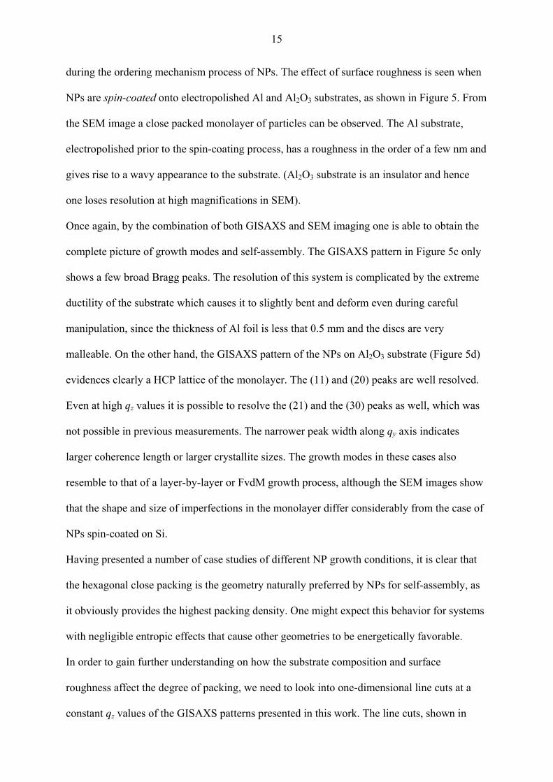
during the ordering mechanism process of NPs. The effect of surface roughness is seen when
NPs are spin-coated onto electropolished Al and Al2O3 substrates, as shown in Figure 5. From
the SEM image a close packed monolayer of particles can be observed. The Al substrate,
electropolished prior to the spin-coating process, has a roughness in the order of a few nm and
gives rise to a wavy appearance to the substrate. (Al2O3 substrate is an insulator and hence
one loses resolution at high magnifications in SEM).
Once again, by the combination of both GISAXS and SEM imaging one is able to obtain the
complete picture of growth modes and self-assembly. The GISAXS pattern in Figure 5c only
shows a few broad Bragg peaks. The resolution of this system is complicated by the extreme
ductility of the substrate which causes it to slightly bent and deform even during careful
manipulation, since the thickness of Al foil is less that 0.5 mm and the discs are very
malleable. On the other hand, the GISAXS pattern of the NPs on Al2O3 substrate (Figure 5d)
evidences clearly a HCP lattice of the monolayer. The (11) and (20) peaks are well resolved.
Even at high qz values it is possible to resolve the (21) and the (30) peaks as well, which was
not possible in previous measurements. The narrower peak width along qy axis indicates
larger coherence length or larger crystallite sizes. The growth modes in these cases also
resemble to that of a layer-by-layer or FvdM growth process, although the SEM images show
that the shape and size of imperfections in the monolayer differ considerably from the case of
NPs spin-coated on Si.
Having presented a number of case studies of different NP growth conditions, it is clear that
the hexagonal close packing is the geometry naturally preferred by NPs for self-assembly, as
it obviously provides the highest packing density. One might expect this behavior for systems
with negligible entropic effects that cause other geometries to be energetically favorable.
In order to gain further understanding on how the substrate composition and surface
roughness affect the degree of packing, we need to look into one-dimensional line cuts at a
constant qz values of the GISAXS patterns presented in this work. The line cuts, shown in

16
Figure 6 for all samples, were taken at qz = 0.9 nm-1, with the exception of the NPs prepared
by sedimentation (see Figure 6d) taken at qz = 0.166nm-1. The Bragg peaks have been indexed
assuming a HCP lattice. For simplicity, the negative qy axis alone is shown, together with
Lorentzian fits to the Bragg peaks. The inverse of the width of the Lorentzian yields the
coherence length of the NP crystallites.
Figure 6: Line cuts at constant qz for NPs self-assembled on: (a) Si, (b) SiO2,(c) Si+
PMMA/MA (33 %), (d) Sedimentation, (e) Al and (f) Al2O3 substrates. Indexing is given
according to a 2-dimensional HCP lattice. The open circles are measured data points and the
solid lines are Lorentzian profile fits to the peaks.

17
The position of the first Bragg peak is similar for all samples. That means that the hexagonal
unit cell has the same lattice constant for different growth modes. The main difference
between the samples is found in the values of long range ordering of the NPs.
Table.2. Comparison of intra-planar distance 10d (calculated from GISAXS pattern) and the
coherence length 10 of (10) planes (calculated from the Lorentzian fit to the peak of width
10 ) for NPs self-assembled on different substrates. The corresponding values for the
substrate PMMA (4%) is not included in the table because it has amorphous like structure.
Table 2 lists the intra-planar distance d(10) calculated for (10) peak from the Lorentzian fitting
and the coherence length of the films from the width of the Lorentzian (ω10) on different
substrates. As expected the sedimentation sample has the maximum coherence length of the
order of 300 nm. In this case the crystal was formed under an equilibrium condition and
shows the maximum ordering.
In all other cases the crystals were formed at a much faster rate and did not have enough time
to form a single crystal, rather forming a continuous film with polycrystalline grain
boundaries. Curiously, the rougher Al and Al2O3 substrate, although promoting monolayer

18
growth with higher density of defects, present a slightly longer correlation length than their Si
sample counterpart.
We can therefore conclude that NP ordering is different on different substrates, revealing a
striking resemblance to atomic growth modes.
The interaction between the solvent and the substrate is the most dominant of all the
interactions. The surface interaction defines the wetting ability of the solvent on different
substrates. Since in the present case toluene is used as a solvent, the "Toluenophobicity" of
the substrate determines, whether the solution will completely wet the surface or form islands
on it. Only in a second step, the ordering or crystallization of NPs takes place. The solvent
(toluene) starts evaporating and NPs form a close packed structure. The crystallization process
is a slow process. Hence, with spin-coating there is not sufficient time for the formation of
large crystals leading to the formation of domains or crystallites. If sufficient time is allowed,
as in the case of a sedimentation process, it is possible to generate three-dimensional "super-
crystals".
Methods:
The iron oxide NPs are chemically synthesized and are purchased from Ocean NanoTech
LLC Company. The mean diameter is 18 nm with a size distribution of 6.5 %. The iron oxide
core is surrounded by oleic acid shell with 2 nm thickness. This surfactant prevents the NPs
from agglomeration. The NPs are dispersed in toluene solvent and are stored in a sealed
bottle.
Samples: The samples were prepared by spin-coating as described in the literature30,31. The
concentration of NP in toluene determined the number of layers formed during spin-coating.
In order to obtain a monolayer the NP dispersion was diluted by pure toluene solvent in 1:1
ratio. Then 0.01 ml of this diluted solution with NPs was taken from the bottle in an oil and
19
silicon free plastic syringe purchased from NORM-JECT® with EROSA disposable
hypodermic needles. Different substrates with typical dimensions of 10 mm2 were used. The
various substrates used for the investigation are silicon (100) substrate with natural oxide
('Si'), silicon (100) with 300 nm silicon dioxide ('SiO2'), silicon(100) spin-coated with
copolymer polymethyl methacrylate/ methacrylic acid (PMMA/MA) with 33 % solid contents
('PMMA_33P'), polymethyl methacrylate (PMMA) with 4% solid contents ('PMMA_4P'),
polished Aluminum ('Al') and a-plane sapphire ('Al2O3'). The Al substrates were prepared
starting from high purity Al foils (Goodfellow, 99.999%), cleaned by sonication in
isopropanol and ethanol for 10 min. The electropolishing of the surface was performed in a
1:3 vol. perchloric acid and ethanol mixture at 10 °C during 10 min, with a constant dc
potential of 20 V applied between the sample and a Pt mesh. The Si and SiO2 substrates were
purchased from CrysTech. The PMMA_33P and PMMA_4P substrates were prepared by
spin-coating PMMA/MA with 33 % solid contents and PMMA with 4% solid contents on Si
substrates at 4000 revolution per minute (rpm) for 30 seconds, respectively. After spin-
coating it was heat-treated at 80° C in air for 20 minutes on a hotplate (Przitherm PR35 with
microprocessor control). The PMMA/MA and PMMA were purchased from Allresist. All
spin-coating processes were performed on a commercial spin-coater from SPIN. The NPs
were spin-coated in two steps. First, the substrate was spun at 300 rpm for 3 seconds and
within 3 seconds the NP solution was drop-cast onto the substrate. This step helps in
spreading the solution uniformly throughout the substrate. In the second step, the rotation was
increased to 4000 rpm with an acceleration of 1000 rpm per second. This step determines the
thickness of the film. Our effort was to keep the volume of NP solution used and the
rotational speed for all the substrates constant. This yields a uniform nominal thickness,
irrespective of the arrangement of the particles. After spin-coating, the samples were also heat
treated at 80° C in air for 20 minutes for the evaporation of the toluene solvent. The
sedimentation sample was prepared in a slightly different way. A PMMA_4P substrate was
20
immersed in a highly diluted solution of NPs. The volume ratio of NP solution to toluene was
1:40000. The beaker containing the substrate and the solution was tightened completely and
the solvent was allowed to evaporate slowly overnight through a small opening at the top.
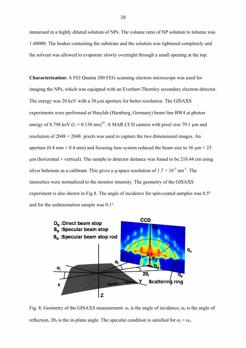
Characterization: A FEI Quanta 200 FEG scanning electron microscope was used for
imaging the NPs, which was equipped with an Everhart-Thornley secondary electron detector.
The energy was 20 keV with a 30 m aperture for better resolution. The GISAXS
experiments were performed at Hasylab (Hamburg, Germany) beam line BW4 at photon
energy of 8.798 keV (= 0.138 nm)32. A MAR CCD camera with pixel size 79.1 µm and
resolution of 2048 × 2048 pixels was used to capture the two dimensional images. An
aperture (0.4 mm × 0.4 mm) and focusing lens system reduced the beam size to 36 µm × 23
µm (horizontal × vertical). The sample to detector distance was found to be 210.44 cm using
silver behenate as a calibrant. This gives a q-space resolution of 1.7 × 10⁻³ nm-1. The
intensities were normalized to the monitor intensity. The geometry of the GISAXS
experiment is also shown in Fig 8. The angle of incidence for spin-coated samples was 0.5°
and for the sedimentation sample was 0.1°.
Fig. 8. Geometry of the GISAXS measurement. i is the angle of incidence, f is the angle of
reflection, f is the in-plane angle. The specular condition is satisfied for i = f.
21
Indexing the lattice: The indexing was performed assuming a two dimensional hexagonal
lattice. The first Bragg peak is the (10) peak and the lattice constant were calculated from the
position of this peak and using the following equation.
hky
hk qkhkh
ad
2
)(3
4 22
Here )(hk corresponds to Miller indices, hkd corresponds to the inter-planar distance, a is
the lattice constant and hkyq is the position of Bragg peak as observed in the experiment.
References:
1. Pulker, H. K. Characterization of Optical Thin Films. Applied Optics 1979, 18, 1969–77.
2. MacLeod, H. A.; MacLeod, A. Thin-Film Optical Filters; 3rd edit.; Taylor & Francis, 2001.
3. Bland, J. A. C.; Heinrich, B. Ultrathin Magnetic Structures, Vol. I-IV; Springer, 2010.
4. Zabel, H.; Bader, S. D. Magnetic Heterostructures (Springer Tracts in Modern Physics); Springer, 2010.
5. Kelly, M. J. Low-Dimensional Semiconductors; Oxford University Press, 1996.
6. Davis, J. H. The Physics of Low-dimensional Semiconductors; Cambridge University Press, 1997.
7. Woodruff, D. P.; Delchar, T. A. Modern Techniques of Surface Science; Cambridge University Press, 1994.
8. Venables, J. A. Introduction to Surface and Thin Film Processes; Cambridge University Press, 2000.
9. Mills, D. L.; Bland, J. A. C. Nanomagnetism: Ultrathin Films, Multilayers and Nanostructures; Elsevier Ltd, 2005.
10. Fert, A.; Grünberg, P. The 2007 Nobel Prize in Physics - Press Release Nobelprize.org.

22
11. Sun, S.; Murray, C.; Weller, D.; Folks, L.; Moser, A. Monodisperse FePt Nanoparticles and Ferromagnetic FePt Nanocrystal Superlattices. Science 2000, 287, 1989–1992.
12. Black, C. T.; Murray, C. B.; Sandstrom, R. L.; Sun, S. Spin-Dependent Tunneling in Self-Assembled Cobalt-Nanocrystal Superlattices. Science 2000, 290, 1131–1134.
13. Shevchenko, E. V; Talapin, D. V; Kotov, N. A.; O’Brien, S.; Murray, C. B. Structural Diversity in Binary Nanoparticle Superlattices. Nature 2006, 439, 55–59.
14. Pileni, M.-P. Self-assembly of Inorganic Nanocrystals: Fabrication and Collective Intrinsic Properties. Accounts of chemical research 2007, 40, 685–93.
15. Nykypanchuk, D.; Maye, M. M.; Lelie, D. van der; Gang, O. DNA-guided Crystallization of Colloidal Nanoparticles. Nature 2008, 451, 549–52.
16. Claridge, S. A.; Castleman, A. W.; Khanna, S. N.; Murray, C. B.; Sen, A.; Weiss, P. S. Cluster-assembled Materials. ACS nano 2009, 3, 244–55.
17. Jones, M. R.; Macfarlane, R. J.; Lee, B.; Zhang, J.; Young, K. L.; Senesi, A. J.; Mirkin, C. a DNA-nanoparticle Superlattices Formed from Anisotropic Building Blocks. Nature materials 2010, 9, 913–7.
18. Ganapathy, R.; Buckley, M. R.; Gerbode, S. J.; Cohen, I. Direct Measurements of Island Growth and Step-edge Barriers in Colloidal Epitaxy. Science (New York, N.Y.) 2010, 327, 445–8.
19. Disch, S.; Wetterskog, E.; Hermann, R. P.; Salazar-Alvarez, G.; Busch, P.; Brückel, T.; Bergström, L.; Kamali, S. Shape Induced Symmetry in Self-assembled Mesocrystals of Iron Oxide Nanocubes. Nano Letters 2011, 11, 1651–6.
20. Dong, A.; Ye, X.; Chen, J.; Murray, C. B. Two-dimensional Binary and Ternary Nanocrystal Superlattices: The Case of Monolayers and Bilayers. Nano letters 2011, 11, 1804–9.
21. Henzie, J.; Grünwald, M.; Widmer-Cooper, A.; Geissler, P. L.; Yang, P. Self-assembly of Uniform Polyhedral Silver Nanocrystals into Densest Packings and Exotic Superlattices. Nature materials 2012, 11, 131–7.
22. Pimpinelli, A.; Villain, J. Physics of Crystal Growth; Cambridge University Press, 1999.
23. Freund, L. B.; Suresh, S. Thin Film Materials: Stress, Defect Formation and Surface Evolution; Cambridge University Press, 2003.
24. Bishop, K. J. M.; Wilmer, C. E.; Soh, S.; Grzybowski, B. A. Nanoscale Forces and Their Uses in Self-assembly. Small 2009, 5, 1600–30.
25. Park, J.; Zheng, H.; Lee, W. C.; Geissler, P. L.; Rabani, E.; Alivisatos, a P. Direct Observation of Nanoparticle Superlattice Formation by Using Liquid Cell Transmission Electron Microscopy. ACS nano 2012, 6, 2078–85.

23
26. Renaud, G.; Lazzari, R.; Leroy, F. Surface Science Reports Probing Surface and Interface Morphology with Grazing Incidence Small Angle X-Ray Scattering. Surface Science Reports 2009, 64, 255–380.
27. Meyerhofer, D. Characteristics of Resist Films Produced by Spinning. Journal of Applied Physics 1978, 49, 3993.
28. Thiele, U.; Vancea, I.; Archer, A. J.; Robbins, M. J.; Frastia, L.; Stannard, A.; Pauliac-Vaujour, E.; Martin, C. P.; Blunt, M. O.; Moriarty, P. J. Modelling Approaches to the Dewetting of Evaporating Thin Films of Nanoparticle Suspensions. Journal of Physics: Condensed Matter 2009, 21, 264016.
29. Choi, J. J.; Bian, K.; Baumgardner, W. J.; Smilgies, D.-M.; Hanrath, T. Interface-induced Nucleation, Orientational Alignment and Symmetry Transformations in Nanocube Superlattices. Nano Letters 2012, 12, 4791–8.
30. Benitez, M. J.; Mishra, D.; Szary, P.; Badini Confalonieri, G. A.; Feyen, M.; Lu, A. H.; Agudo, L.; Eggeler, G.; Petracic, O.; Zabel, H. Structural and Magnetic Characterization of Self-assembled Iron Oxide Nanoparticle Arrays. J. Phys.: Condens. Matter 2011, 23, 126003.
31. Mishra, D.; Benitez, M. J.; Petracic, O.; Badini Confalonieri, G. A.; Szary, P.; Brüssing, F.; Theis-Bröhl, K.; Devishvili, A.; Vorobiev, A.; Konovalov, O.; et al. Self-assembled Iron Oxide Nanoparticle Multilayer: X-ray and Polarized Neutron Reflectivity. Nanotechnology 2012, 23, 055707.
32. Roth, S. V.; Döhrmann, R.; Dommach, M.; Kuhlmann, M.; Kröger, I.; Gehrke, R.; Walter, H.; Schroer, C.; Lengeler, B.; Müller-Buschbaum, P. Small-angle Options of the Upgraded Ultrasmall-angle X-ray Scattering Beamline BW4 at HASYLAB. Review of Scientific Instruments 2006, 77, 085106.