superlattice and negative differential conductivity in semiconductors
TRANSCRIPT

8/9/2019 Superlattice and Negative Differential Conductivity in Semiconductors
http://slidepdf.com/reader/full/superlattice-and-negative-differential-conductivity-in-semiconductors 1/5

8/9/2019 Superlattice and Negative Differential Conductivity in Semiconductors
http://slidepdf.com/reader/full/superlattice-and-negative-differential-conductivity-in-semiconductors 2/5
Conduction
(b)
Figure 1 Electron nergy n the valence nd onduction
bands s a function of distance in the direction of the
superlattice fo r (a) alternation of donor andacceptor im-
purities and (b) periodic varia tion of lloy com position.
Solid nddashedines epresent inusoidal ndperiodic
square-wellpotentials, espectively. The
E ,
are the mag-
nitudes
of
the energygap n the semiconductor materials
used and
VI
is theamp litude of theperiodic uperlattice
potential.
pound s an d their alloys, etc. The re may be
a
number of
ways to form a superlattice structure.* We considered
two methods: (1) a periodic variation of don or or cceptor
impurities, alternately, in
a
single semiconduc tor; and (2)
a
periodic v ariation of alloy composition, introduced during
the crystal growth. Both methodscouldbe used simul-
taneously and
it
would be advantageous
to
carry out the
epitaxial growth at a relatively low temperature' to mini-
mize the therm al diffusion of impurities o r alloy constit-
uents, which would tend to wash out the desired potential
profile. In this context, t is mo re desirable to apply method
(2) because of the lower diffusion coefficients in alloys.
forms known as polytypes, in which one sees a kind of one-dimensional
* Some crystals such as hexagonal SIChave a number of different structural
type of crystal. The potential amplitude and resulting energy gap are probably
superlattice structure. The periods range from 15 to 53A,depending on the
too small to demonstrate any of the effects described here.
62
L. ESAKI AND
R. TSU
In the alternating impurity system (Fig. la), the peak-
to-peak amplitude of the periodic p otential can be hosen,
in principle, as any value up to that of the energy gap,
whereas, in the alternating alloy com position system (Fig.
lb ) , t hevalue would be limited to abo uthalf of the differ-
ence between the energy gaps of the twomaterials involved.
It would not be possible to ob tain the desired superlattice
structure (with a 100-A period and a 0.1-eV potential
amplitude) with relatively light doping because of space
charge effects.
We considered two potential functions, sinusoidal wave
and
a
periodic square wave, as illustrated in Fig.
1,
a n d
two typ ical values of effective m ass, 0.025mo an d
0.07m0,
which are applicable to the InAs-based alloy an d GaAs-
based alloy systems, respectively. The Ge-GeSi system is
also attractive, particularly from an experimental point
of
view. W e would choose relatively pur e elemental or binary
compound semiconductors as the narrower gap semicon-
ductor, corresponding o th e alleys in the otential profile,
to ob tain a favorable electron scattering time.
Band
structure
We are concerned with the energy bands in a one-dimen-
sional uperlattice represented by a periodicpotential
V(x)
=
V(x
f nd
with a period d typically 10 to 20 times
greater than the lattice constant
a
in the host crystal. The
usual Brillouin zone will be subdivided into minizones as
shown in Fig. 2a. Since we ar e interested only i n t he first
minizone, because of low carrier concentrations we may
assume that the E-k relation in the directions parallel
to
the superlattice planes is parabolic as usual. For the sinu-
soidalpotential V(x)
=
Vl [cos (27rxld) - 11, the wave
equ ation in the irection of the superlattice, denoted by x,
has the fo rm of Mathieu's equation and has been studied
in great detail by Slater.3
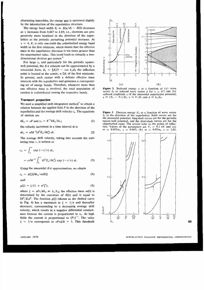
Th e reduced energy an d amplitude of the perturbing
periodic potential are defined by
=
q(k,) = (E, - Vl)/Eo
and y = V,/Eo, respectively, where
VI
is the am plitude of
the periodic superlattice potential and Eo
=
ktk:/2m; here
kd = 7r/d and m is the effective mass. In Fig. 2b we plot
r ]
vs. y for the sinusoidalpotential, using a parameter
/3 = k,/kd. Th e allowed solutions of th e wave equation
are represented by the non-shaded regions, while the for-
bidden solutions fall n the shaded regions. For the case of
y = 0.5, 7 vs. is plotted in Fig. 2a.
We also calculated the energy-momentum relation for
the periodic square-wel l p~tent ia l ,~sing the expression
given by Smith.5 A co mparison o f the E-vs.-k curves
for the two otentials is shown in Fig. 3, where d
=
loo
VI =
O.leV, and m
=
0.025mo (Fig. 3a) a nd
o.07m0
(Fig. 3b). The zeros of the energy scales in Fig. 3 are
set at the bot tom of the conduction band in the narrower
energy-gap material.Therefore th e first ban d is moved
up by anamo unt slightly less than
Vl.
In he case of
IBM
J RES. DEVELOP.
8/9/2019 Superlattice and Negative Differential Conductivity in Semiconductors
http://slidepdf.com/reader/full/superlattice-and-negative-differential-conductivity-in-semiconductors 3/5
alternating impurities, the energy gap is narrowed slightly
by the introduction of the superlattice structure.
The energy band width El =
E ?r/d)
- E(0) decreases
as increases from 0.667 to 1.85; i.e., electrons are pro-
gressively more localized in he direction of the super-
lattice as the periodic perturbing potential increases. At
y
=
4, El is only one-tenth the unperturbed energy band
width in the first minizone, which means that the effective
mass in the superlattice direction
is
ten times greater than
the unperturbed value. This trend leads to virtually a two-
dimensional electron gas system.6
For large y, and particularly for the periodic square-
well potential, the E-k relation can be approximated by a
sinusoidal form, E,
=
$E1(l - cos k,d); the inflection
point is located at the center, ?r/2d,of the first minizone.
In general, each carrier with a definite ffective mass
interacts with the superlattice and generates a correspond-
ing set of energy bands. Therefore, whenever more than
one effective mass
is
involved, the otal population of
carriers is redistributed among the respective bands.
Transport properties
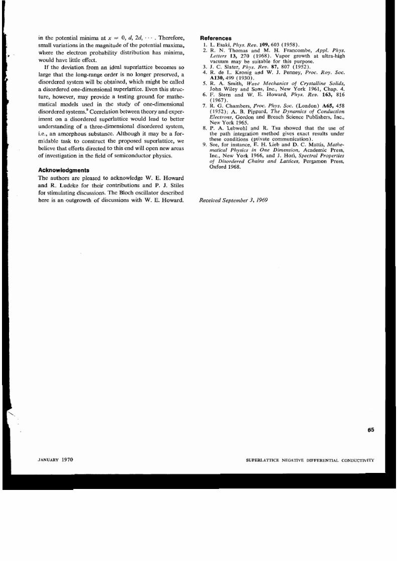
We used a simplified path integration method7 to obtain a
relation between the applied field F i n the direction of the
superlattice and the average drift velocity u . The equations
of motion are
- h k z =
eF
and
u
=
h dE,/dk,; 1 )
the velocity increment in a time interval dt is
du, = eFh-2 (d2E, / ak~)
t.
2)
The average drift velocity, taking into account the scat-
tering time T is written as
ud
=
lm
xp (- t / r du
=
eFh-' lmd'E, /dk;) exp (- t / r t . 31
Using the sinusoidal E-k approximation, we obtain
Od
g ( l ) [ h k d / m ( o ) ] 4)
and
dl
=
E / 1
+
T212>
5 )
where = eFr/hkd
=
k , / k d ; the effective mass
m(0)
is
determined by the curvature
of E ( k )
and
is
equal to
2h2/E1d2. he function g 4) (shown as the dashed curve
in Fig. 4 has maximum at =
l/?r
and thereafter
decreases, corresponding to a decreasing average drift
velocity, which results in a negative differential conduct-
ance because the current is proportional to
vd.
At high
fields the current isproportional to ( F T ) - ~ . he value
=
l / r corresponds to eFrd/h = 1 This threshold
(j = ,
9 ;
-
_
, x:R
4 -----
Figure
2 Reduced energy asunction of (a) wave
vector k , or reduced wave vector
p
for y = 0.5 and (b)
reduced amplitude y of the sinusoidal superlattice potential;
=
E ,
-
VI)
/ E o ,
y
=
V J E 0
and p
k, /ka.
Figure
3
Electron energy E, as a function of wave vector
k ,
in the direction of the superlattice. Solid curves are for
the sinusoidal potential, long-dash curves are for theperiodic
square-well potential, and the short-dash curves are for the
unperturbed cases. The arrows refer to the points of inflec-
tion. Values
of
theparameters are
VI
= 0.1 eV and
a)
rn =
0.025rno, y
=
0.667; (b)
rn =
0.07rno, y
= 1 85
/6
I
/'
.
-
2d
d
2d
7
7 317
,(
.*
6
JANUARY 1970
SUPERLATTICE
NEGATIVE
DIFFERENTIAL
CONDUCTIVIT

8/9/2019 Superlattice and Negative Differential Conductivity in Semiconductors
http://slidepdf.com/reader/full/superlattice-and-negative-differential-conductivity-in-semiconductors 4/5
I
Figure 4 Drift velocitymplitudes
as
functions of the
reduced parameter =
2 e F ~ d / h k , / k d :
(a) sinusoidal
potential; (b) periodic quare-wellpotential for
k , / k d =
0.5; and
(c)
periodic quare-well potential for
k i / k d
=
0.82.
Here
ki
is the wave vector at the inflectionpoint of
the E-k curve.Arrowsndicatehe eaks of the drift
velocity functions.
condition can be achieved with a n electric field strength
F = lo3
V/cm and
a
scattering time
T =
0.67psec.
For
small
y,
when
E k)
is not a sinusoidal function,
the
E-k
relation was approximated by sections of two
parabolas of opposite curvature, joined at the inflection
point
Ei , k i ) .
or the average drift velocity in this case
we obtained
and
Th e functionf(() is plotted in Fig. 4 for
k i /kd
=
0.82 (y
=
0.667) and 0.50 (y
=
1.85). These curves also indicate th e
existence of negative conductance, but the hreshold value,
2
0.4
or
eFrd/A
2
1.26
for the top curve, is slightly
greater tha n or he sinusoidal
E-k
relation. Since the
inflection point is shifting tow ard the minizone boun dary,
it is understandable that higher fields or longer scattering
times are required to obtain negative conductance.
As
the a pplied voltage is increased, howe ver, effects such
as Zener tunneling, avalanching and impact ionization set
in; eventually the negative conductance would be offset
by these effects. The possibility of Zener tunneling
to
the
64
second minizone when electronseach the first minizone
L. ESAKI AND R.
TSU
boundary could be a dominant factor in thecase of small
amplitude of the periodic potential. If,however, the am pli-
tude VI is of the orde r of 0.leV an d the applied field is
of the order of
lo3
V/cm, the tunneling probability can
be kept negligibly small. If the electron scattering time is
sufficiently long, electron s will undergo rf oscillation du e
to th e reflection at the minizone boundaries, the so-called
Bloch oscillation. This occur s fo r
eFrd/A >
27r, which
is several times the threshold value for negative conduct-
ance. Th e frequency of the Bloch oscillator is
eFd/h = 250
GHz for
F
= 103V/cm an d
d
=
l O O A .
The scattering
time then should be greater than 4 psec.
Discussion
In obtaining the solutions fo r the average drift velocity,
Eqs. 4 and
6 ,
we made twoassumptions; namely, that
k, =
eFf /A and tha t T is time-independent. The form er
assumption implies that k ,
= 0
a t
t
=
0,
which is justifiable
in relatively lightly do ped semiconductors.' The atte r
assumption is
a
reasonable approxim ation in the case in
which the allowed ban d width is ma de narrow.
In
the two
examples, m
=
0.025m0
and o.07m0, the smallermass
case equires an electron temperature close
to
1000 K,
whereas the larger mass case requiresonly
100 K,
t o
reach the negative differential conductivity region. This
electron temperature, which is also a function f the ampli-
tud e and the profile of the periodic potential, could be
kept very low with proper design of the structure. In such
cases the specimen could be operated with low electric
fields at cryogenic temperatures; ower emperatures are
helpful in obtaining onger cattering times.
Using th e Heisenberg uncertainty principle we estimated
the values of electron scattering time
T
and the mean free
path I that are required for these quantum mechanical
effects. For
AE
=
O.lE,
=
0.003
eV and
Ak
=
O.lkd
=
3
X
lo5
cm-', the inequalities are I2
330A
and
r 2 0.22
psec. This indicates that the mean free path should be at
least three times as long as the superlattice spacing. The
scattering time here is abo ut one-third
of
that previously
estimated for obtaining anegative differential conductance.
The scattering time
is
an impor tant factor in the effects
described and more-detailed calculations are being made
to verify the model. If the superlattice were perfect, the
scattering ime would be infinite, as is the case with an
idealcrystal lattice. Small deviations fro m he perfect
periodic potential, even when the long-range ord er is pre-
served, act as localized scattering centers. If the super-
lattice structure is prepared by
a
periodicvariation of
alloy composition, there will be unavoidable an dom varia-
tions in the magnitude of the thereby introduced super-
lattice potential maxima (at =
d/2,3d/2, . ).
However,
the probability density of conductionelectrons in he
superlattice structur e of the sinusoidal potential indicates
that electrons in the conduction ba nd would be bunched
IBM J .
RES.
DEVELOP.
8/9/2019 Superlattice and Negative Differential Conductivity in Semiconductors
http://slidepdf.com/reader/full/superlattice-and-negative-differential-conductivity-in-semiconductors 5/5
in the potential minima at
x
=
0
, 2 d , . Therefore,
small variations in themagnitude of the potential maxima,
where the electron probabilitydistribution has minima,
would have little effect.
If the deviation fro m an ideal superlattice becomes so
large that the long-range order is no longer preserved, a
disordered system will be obtained, w hich might be called
a
disordered one-dimensional superlattice. Even this struc-
ture, however, may provide
a
testing ground for mathe-
matical models used in he study of one-dimensional
disordered systems.' Correlation between theory an d exper-
iment on a disordered superlattice would lead to better
understanding of a three-dimensional disordered system,
i.e., an am orpho us substance. A lthough it may be a for-
midable task
to
construct the proposed superlattice, we
believe th at efforts directed
to
this end will ope n new areas
of investigation in the field of semiconductor physics.
Acknowledgments
The autho rs are pleased to acknowledge
W.
E. Howard
and R. Ludeke for theircontributions and P. J. Stiles
for stimulating discussions. Th e Bloch oscillator described
here is an outgrowth of discussions with W. E. Howard.
J A N U A R Y
1970
References
1 . L. Esaki, Phys . Rev . 109,603 1958).
2.R.N. Thomas and M. H. Francombe, Ap p l .Pkys .
Letters 13, 70 1968). Vapor rowth at ultra-high
vacuum may be suitable for this purpose.
3. J C . Slater, Phys .Rev . 87, 807 1952).
4.R. de
L.
Kronigand W. J Penney, Proc .Roy . SOC
A130,499 1930).
5. R. A. Smith,
Wave Mechanics of CrystallineSolids,
John
Wileyand Sons, Inc., New York 1961, Chap.
4.
6.
F.
Stern nd
W. E.
Howard,
Pkys .Rev .
163, 816
1967).
7. R. G. Chambers, Proc.Phys.SOC. London)A65, 458
1952);A. B. Pippard,
TheDynamics
of
Conduction
Electrons, Gordon and Breach Science Publishers,
Inc.,
New York 1965.
8. P.A. Lebwohl and R. Tsu showed thathe use of
the path ntegration method gives exact results under
these conditions private communication).
9. See,
for
instance, E. H. Lieb and D. C . Mattis, Mathe-
maticalPhysics in OneDimension,
Academic Press,
Inc.,
New
York
1966, and J.
Hori, Spectral Properties
of
DisorderedChains and Lattices, Pergamon Press,
Oxford 1968.
Received September 3,
1969
6
SUPERLATTICE
NEGATIVE DIFFERENTI AL CONDUCTIVI