investigation to improve the control and operation of a
TRANSCRIPT

Technological University Dublin Technological University Dublin
ARROW@TU Dublin ARROW@TU Dublin
Doctoral Engineering
2011
Investigation to Improve the Control and Operation of a Three-Investigation to Improve the Control and Operation of a Three-
phase Photovoltaic Grid-tie Inverter phase Photovoltaic Grid-tie Inverter
Mohamed Moin Hanif Technological University Dublin, [email protected]
Follow this and additional works at: https://arrow.tudublin.ie/engdoc
Part of the Electrical and Computer Engineering Commons
Recommended Citation Recommended Citation Hanif, M. (2011) Investigation to Improve the Control and Operation of a Three-phase Photovoltaic Grid-tie Inverter. Doctoral Thesis. Technological University Dublin. doi:10.21427/D7JC80
This Theses, Ph.D is brought to you for free and open access by the Engineering at ARROW@TU Dublin. It has been accepted for inclusion in Doctoral by an authorized administrator of ARROW@TU Dublin. For more information, please contact [email protected], [email protected].
This work is licensed under a Creative Commons Attribution-Noncommercial-Share Alike 4.0 License

i
DEDICATED TO MY PARENTS
AND
MY WIFE
ii
Abstract
Solar Energy or more precisely photovoltaic energy is one of the most promising
sources of electricity for the future and it can be used as a distributed generator (DG) to
play its role in ‘smart grids of the future’. Distributed PV (photovoltaic) generators can
provide numerous potential benefits such as augmenting the capacity of distribution
systems, deferring capital investments on distribution and transmission (T&D) systems and
improving power quality and system reliability. The PV energy which possesses very
special I-V and P-V characteristics has to be conditioned by a PV inverter before it can be
consumed by an ac load and/or the grid. Technical improvements in maximum power point
tracking (MPPT) and islanding detection are proposed for a three-phase photovoltaic grid
tied inverter (GTI) keeping in mind the requirements of the international standards for
connecting a DG to the utility grid. This PhD thesis will contain four major sections which
are briefed below.
A three phase GTI has been simulated using Matlab/Simulink to test the various
control blocks and algorithms involved in the building of the power conditioning unit. A
DS1104 dSpace DSP controlled, 5.625 kW three-phase GTI laboratory prototype has then
been built. Various hardware components, including inverter switches, gate drivers, LCL
filter, rectified dc source, boost circuit, transformer, 16A current protection circuit,
additional sensing interface circuits and PWM level shifter have been designed and built
within the laboratory. The software algorithm created in Simulink communicates directly
with the built hardware via the graphical user interface that has been designed with dSPace
Control Desk. Algorithms have been developed for the inverter in order to protect it from
operating out of nominal frequency and voltage ranges. An algorithm has been developed

iii
to ensure the boost dc link voltage is controlled to 300V when dc voltage source varies
between 150V and 265V.
The Z-Source inverter (ZSI), with nine operating states that employs an extra shoot
through (ST) state compared to the eight states (6 active and 2 zero states) in traditional
VSI is one of the most recent boost topologies that has been proposed in the literature. A
step by step design procedure of a ZSI has been developed. A topology comparison
between Z-Source inverter and dc-dc boost with VSI is done using literature and
simulations. Merits and demerits of the two topologies are summarised and the choice of
the topology is justified.
MPPT is a process by which maximum power from a PV panel or array is tracked
and absorbed during a particular weather condition (insolation level and temperature).
There are various MPPT techniques in the literature which are reviewed and a new MPPT
approach based on the P&O (Perturb and Observe) method is proposed. The proposed
technique is tested on the three phase GTI simulation, it is analysed and compared to the
conventionally reviewed P&O MPPT approach.
The issue of islanding of GTI’s has raised concerns of equipment and personal
safety, for which reason the inverter has to detect and stop the inverter during loss of grid.
Passive techniques can detect the grid failure quite well when there is a large power
mismatch between the DG and the load but not when the mismatch is small. Active
techniques can work well with lower levels of power mismatch but they degrade power
quality by introducing disturbances into the power system. A novel wavelet based anti-
islanding technique is proposed and incorporated into the running hardware protection.
This uses physical measurements to reduce the non-detection zone close to zero and keep
the power quality of the inverter output unchanged. The developed algorithms have been
validated in the laboratory prototype and yield very satisfactory performance.

iv
Declaration
I certify that this thesis which I now submit for examination for the award of the Degree of
Doctor of Philosophy, is entirely my own work and has not been taken from the work of
others save and to the extent that such work has been cited and acknowledged within the
text of my work.
This thesis was prepared according to the regulations for postgraduate study by research of
the Dublin Institute of Technology and has not been submitted in whole or in part for an
award in any other Institute or University.
The work reported on in this thesis conforms to the principles and requirements of the
Institute's guidelines for ethics in research.
The Institute has permission to keep, to lend or to copy this thesis in whole or in part, on
condition that any such use of the material of the thesis be duly acknowledged.
Signature __________________________________ Date ________________________
Candidate

v
Acknowledgement
I take this opportunity to express my sincere gratitude to all those people who
directly or indirectly helped me to carry out this research work successfully.
I am grateful to Dublin Institute of Technology for offering me with full scholarship to
carry out doctoral research in the School of Electrical Engineering Systems.
I am very fortunate to carry out my research work under the fantastic supervision of Dr
Malabika Basu and Mr. Kevin Gaughan. Dr. M. Basu’s dedication to research and Mr.
Kevin Gaughans’s practical hardware experience has driven me to reach my research
targets with ease. I would like to thank them both for their invaluable guidance, support
and encouragement at every stage of this research work. I would also like to thank Dr. M.
Basu for her kind patience, support and advice with non-work related problems.
As an advisory supervisor Dr. Michael Conlon was always there to hold discussions and
make suggestions through out the research period. I would also like to thank Prof. Eugene
Coyle for his friendly support during my entire time here in Dublin.
I am thankful to my previous colleagues Dr. Iurie Axente and Dr. Jayanti Navilgone
Ganesh for helping me familiarise myself with the laboratory and their experience with
research during my first year. I would also like to thank my colleagues Mr. Shafiuzzaman
Khan Khadem, Mr. Nasif Shams, Dr. Umakant Dwivedi and Mr. Gabriel Garus for their
technical discussions, suggestions and help with use of tools and equipment within the
laboratory.
I would also like to thank the laboratory technicians Mr. Terrence Kelly and Mr. Finbarr
O’Meara for all their help and co-operation in lending tools and ordering electrical and
electronic components.

vi
Finally I would like to thank my family: My parents who educated and encouraged me to
be what I am today. For their unconditional and priceless support with education and
research, for their love and caring, for listening to all my problems and frustration very
patiently and being there for me during all times. My wife for her love, patience and
tolerating my long hours of absence from home, for her support and encouragement from
the time we have known each other. My siblings for all their encouragement, love, caring
and support through out.

vii
List of Abbreviations
PV Photovoltaic
T&D Transmission and distribution
GTI Grid-tie inverter
ZSI Z-source inverter
VSI Voltage source inverter
CSI Current source inverter
MPP Maximum power point
MPPT Maximum power point tracking
ICT Incremental conductance technique
P&O Perturb and observe
CRV Constant reference voltage
DSP Digital signal processor
NDZ Non-detection zone
DG/DER Distributed generation/Distributed energy resource
PWM Pulse width modulation/modulated
PCC Point of common coupling
PLL Phase lock loop
THD Total harmonic distortion
GUI Graphical user interface
ADC Analogue to digital converter
ST Shoot-through
CMR Common mode rejection

viii
OVP/UVP Over/Under voltage protection
OFP/UFP Over/Under frequency protection
SMS Sliding mode frequency shift
AFD Active frequency drift
SFS Sandia frequency shift
DWT Discrete wavelet transform
WBA Wavelet based analysis
RMAC Root mean absolute of wavelet coefficients
DRMAC Difference in root mean absolute of wavelet coefficients
PCS/PCU Power conditioning system/unit

1
Contents
Abstract ............................................................................................................................... ii
Declaration..........................................................................................................................iv
Acknowledgement ...............................................................................................................v
List of Abbreviations......................................................................................................... vii
Contents ...............................................................................................................................1
List of Figures ......................................................................................................................7
List of Tables......................................................................................................................13
List of Symbols ..................................................................................................................14
1. INTRODUCTION .........................................................................................................17
1.0 General introduction............................................................................................... 17
1.1 Focus of research.................................................................................................... 19
1.2 Research contribution............................................................................................. 21
1.3 Organization of the thesis....................................................................................... 22
2. THREE PHASE PHOTOVOLTAIC GRID CONNECTED INVERTER .....................25
2.0 Introduction ............................................................................................................ 25
2.1 Photovoltaic source ................................................................................................ 25
2.2 Maximum power point tracker ............................................................................... 28
2.3 Inverter control types ............................................................................................. 29
2.3.1 Voltage control ................................................................................................ 30
2.3.2 Current control................................................................................................. 30
2.4 Power transfer theory ............................................................................................. 31
2.4.1 Real power flow............................................................................................... 32

2
2.4.2 Reactive power flow........................................................................................ 33
2.5 Synchronization and control of three phase grid connected inverter system......... 34
2.6 Symmetrical components ....................................................................................... 35
2.7 Voltage source inverter .......................................................................................... 36
2.7.1 Generation of PWM pulses.............................................................................. 37
2.8 Management of dc link voltage.............................................................................. 38
2.9 Standards for micro generation in the Republic of Ireland .................................... 41
2.10 Modelling of three phase grid connected photovoltaic inverter........................... 45
2.10.1 Simulink......................................................................................................... 45
2.10.2 The PV model................................................................................................ 48
2.10.3 MPPT control block....................................................................................... 49
2.10.4 Design of dc-dc boost circuit......................................................................... 51
2.10.5 Model of PWM inverter ................................................................................ 54
2.10.6 Model of LCL filter ....................................................................................... 54
2.10.7 Coupling impedance ...................................................................................... 56
2.10.8 DC link controller.......................................................................................... 56
2.10.9 List of simulations carried out ....................................................................... 57
2.11 Control program ................................................................................................... 58
2.12 Simulation and results .......................................................................................... 61
2.13 DSP....................................................................................................................... 69
2.13.1 Choice of DSP ............................................................................................... 72
2.14 Conclusion............................................................................................................ 73

3
3. TOPOLOGY COMPARISON BETWEEN Z-SOURCE INVERTER AND DC-DC
BOOST WITH VOLTAGE SOURCE INVERTER...........................................................74
3.0 Introduction ............................................................................................................ 74
3.1 Boost converter ...................................................................................................... 74
3.1.1 Choice of capacitor and inductor..................................................................... 77
3.2 Z-Source inverter.................................................................................................... 78
3.2.1 Z-Source inverter operation............................................................................. 79
3.2.2 ZSI circuit equations........................................................................................ 81
3.2.3 Alternate equations for Z-Source inverter ....................................................... 83
3.2.4 Z-network component design .......................................................................... 83
3.2.5 Shoot-through (ST) control ............................................................................. 85
3.2.6 ZSI self-boost phenomenon............................................................................. 88
3.3 Simulations of VSI (with boost) and ZSI............................................................... 91
3.4 Comparison of VSI (with boost) and ZSI .............................................................. 96
3.5 Choice of boost converter for the hardware prototype........................................... 98
3.6 Conclusion.............................................................................................................. 99
4. NEW MAXIMUM POWER POINT TRACKING APPROACH BASED ON
PERTURB AND OBSERVE METHOD .........................................................................100
4.0 Introduction .......................................................................................................... 100
4.1 Maximum power point tracker review ................................................................. 101
4.2 MPPT technique................................................................................................... 104
4.2.1 Conventionally adopted P&O method........................................................... 105
4.2.2 Novel AC side P&O MPPT technique .......................................................... 106

4
4.2.3 Algorithm for MPPT ..................................................................................... 108
4.3 Simulation results................................................................................................. 110
4.4 Conclusion............................................................................................................ 113
5. IMPLEMENTATION OF THE THREE-PHASE GRID CONNECTED INVERTER:
HARDWARE, SOFTWARE AND CONTROL ..............................................................114
5.0 Introduction .......................................................................................................... 114
5.1 Implementation of a laboratory prototype............................................................ 115
5.1.1 Power circuit configuration and components parameters.............................. 115
5.1.2 Variable rectified dc source ........................................................................... 117
5.1.3 Inverter........................................................................................................... 117
5.1.4 Boost switch and diode.................................................................................. 118
5.1.5 Boost inductor and capacitor ......................................................................... 118
5.1.6 Step down transformer................................................................................... 120
5.1.7 Filter inductors............................................................................................... 120
5.1.8 Filter capacitors ............................................................................................. 121
5.1.9 Switching device protection .......................................................................... 122
5.1.10 Cabinet and front measurement panel ......................................................... 122
5.1.11 Interface circuits .......................................................................................... 123
5.1.12 Auxiliary dc source to power the circuits .................................................... 124
5.1.13 Circuit breakers............................................................................................ 124
5.1.14 Design and fabrication of the current protection circuit.............................. 125
5.1.15 Design and fabrication of the measurement interface circuitry................... 127
5.1.16 Design and fabrication of the PWM level shifter ........................................ 140

5
5.2 Software control (Simulink control program and dSpace DS1104 controller) .... 142
5.2.1 Control program ............................................................................................ 143
5.2.2 DC link voltage control ................................................................................. 144
5.2.3 Inverter protection ......................................................................................... 145
5.2.4 Control flow chart.......................................................................................... 147
5.2.5 Software development ................................................................................... 148
5.3 Construction and testing....................................................................................... 151
5.4 Experimental results of the interface circuits ....................................................... 155
5.5 Experimental results of the system....................................................................... 158
5.6 Conclusion............................................................................................................ 165
6. NOVEL ANTI-ISLANDING TECHNIQUE PROPOSED USING WAVELET
ANALYSIS ......................................................................................................................166
6.0 Introduction .......................................................................................................... 166
6.1 Review of islanding detection .............................................................................. 167
6.1.1 Passive methods............................................................................................. 167
6.1.2 Active methods .............................................................................................. 172
6.2 Analysis of mismatched power during islanding ................................................. 178
6.3 Proposed anti-islanding technique using wavelet analysis .................................. 180
6.3.1 Wavelet transform ......................................................................................... 181
6.3.2 Proposed algorithm........................................................................................ 183
6.3.3 System setup .................................................................................................. 187
6.3.4 Simulation results .......................................................................................... 189
6.3.5 Experimental results ...................................................................................... 195

6
6.4 Conclusion............................................................................................................ 199
7. CONCLUSION AND FUTURE WORK.....................................................................200
7.1 Conclusion............................................................................................................ 200
7.2 Future work .......................................................................................................... 203
References........................................................................................................................204
Appendix 1: Three phase grid connected PV system with P&O MPPT.........................215
Appendix 2: dc-dc boost with VSI...................................................................................219
Appendix 4: Three phase grid connected PV system with novel AC side P&O MPPT..222
Appendix 5: Software control program run on dSPace DS1104 .....................................223
Appendix 6: Hardware.....................................................................................................232
Appendix 7: dSpace block set and Control Desk.............................................................237
Appendix 8: List of publications......................................................................................238

7
List of Figures
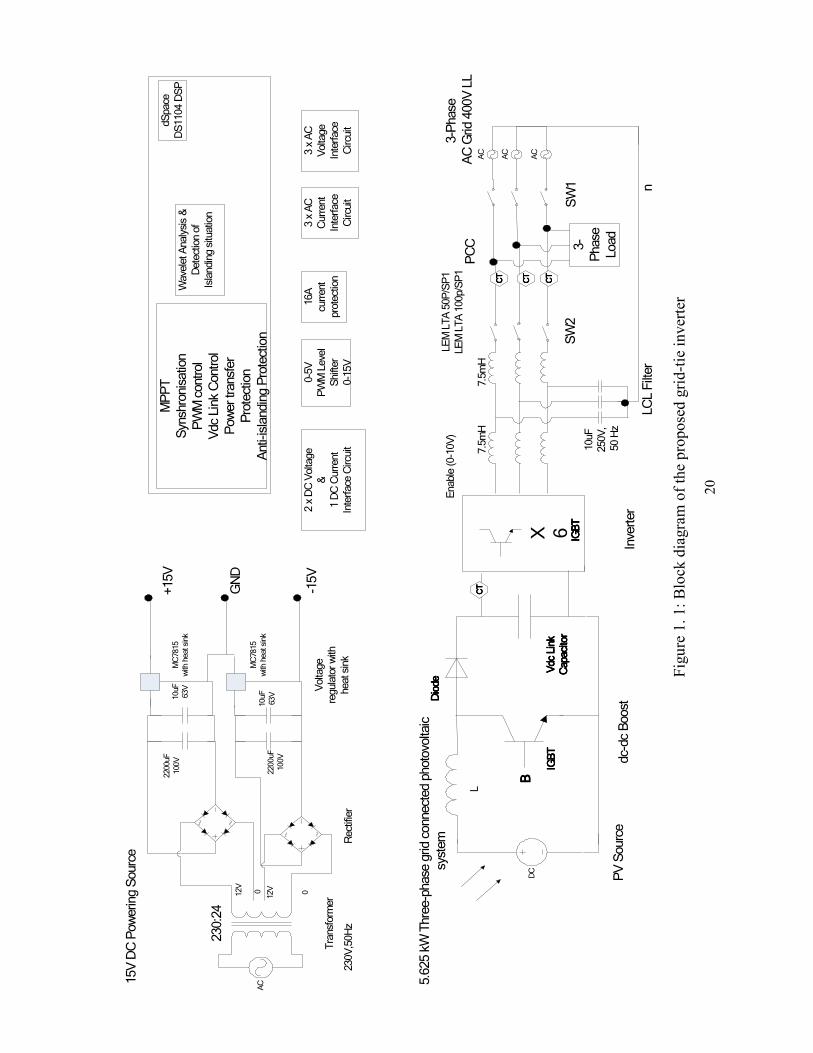
Figure 1. 1: Block diagram of the proposed grid-tie inverter .......................................... 20
Figure 2. 1: I-V curve of a solar cell [7]-[14] .................................................................. 26
Figure 2. 2: (a) Solar cell equivalent circuit, (b) Inverted diode characteristic ............... 26
Figure 2. 3: (a) PV panel insolation characteristic (b) PV panel temperature characteristic
[15]................................................................................................................................... 27
Figure 2. 4: System integration of PV power conditioning system ................................. 29
Figure 2. 5: Power flow between two AC sources........................................................... 31
Figure 2. 6: Ideal three-phase voltage vector................................................................... 34
Figure 2. 7: Showing (1 of the 3 Phases) one phase of control voltage waveforms to
modulate pulse widths...................................................................................................... 38
Figure 2. 8: Screen shot of MATLAB & Simulink environment .................................... 47
Figure 2. 9: Typical I-V & P-V characteristics with typical values for an array [16]...... 48
Figure 2. 10: PV model designed in Simulink. ................................................................ 49
Figure 2. 11: The design of MPPT block......................................................................... 50
Figure 2. 12: DC-DC boost circuit model for simulation ................................................ 51
Figure 2. 13: 3-leg inverter block and its properties........................................................ 54
Figure 2. 14: Selection of LCL filter values .................................................................... 55
Figure 2. 15: Control program used for simulation of grid connected PV inverter......... 60
Figure 2. 16: PLL tracking capability .............................................................................. 64
Figure 2. 17: Vcap maintained at 780V............................................................................. 65
Figure 2. 18: Iref changed according to the available power ............................................ 65

8
Figure 2. 19: Power from PV extracted at MPP, tracked using the MPPT algorithm..... 65
Figure 2. 20: Operating Vpv against time........................................................................ 66
Figure 2. 21: Operating Ipv against time ......................................................................... 66
Figure 2. 22: Inverter voltage and current ....................................................................... 66
Figure 2. 23: Grid voltage and injected grid current........................................................ 67
Figure 2. 24: PV inverter and grid together supply power to the load until islanded at
0.4s. .................................................................................................................................. 67
Figure 2. 25: Frequency at PCC, large mismatch at 0.4s................................................. 68
Figure 2. 26: PV inverter and grid together supply power to the load until islanded at
0.4s (large mismatch)....................................................................................................... 68
Figure 2. 27: Block diagram of Texas Instrument DSP controller TMS320F2812......... 70
Figure 2. 28: Block diagram of the dSPace DSP controller DS1104 ............................. 71
Figure 3. 1: Boost converter............................................................................................. 76
Figure 3. 2: Waveforms of current and voltage in a boost converter operating in
continuous mode. ............................................................................................................. 77
Figure 3. 3: General configuration of a ZSI [30] ............................................................. 79
Figure 3. 4: Equivalent circuits of ZSI: (I) Non–Shoot-through mode (II) Shoot-through
mode [31] ......................................................................................................................... 80
Figure 3. 5: Sketch map of simple control [36] ............................................................... 86
Figure 3. 6: Sketch map of maximum boost control [36], [37] ....................................... 87
Figure 3. 7: Sketch map of maximum constant boost control [36].................................. 87
Figure 3. 8: New operation modes during self-boost [26] ............................................... 90

9
Figure 3. 9: VSI with boost converter simulation results ................................................ 93
Figure 3. 10 : ZSI simulation results................................................................................ 94
Figure 3. 11 : VL1 and VC1 during shoot through .......................................................... 95
Figure 3. 12: (a) DC link voltage of the ZSI (b) zoomed in from 0.03s to 0.0325s ........ 95
Figure 4. 1: Basic MPPT system.................................................................................... 101
Figure 4. 2: PV array and load characteristics ............................................................... 101
Figure 4. 3: Conventional MPPT controller using open circuit voltage Voc ................. 102
Figure 4. 4: MPPT controller for the conventional method and novel proposed approach
........................................................................................................................................ 105
Figure 4. 5: MPPT controller for the conventional method........................................... 106
Figure 4. 6: Sketch of I-V and P-V characteristic of a PV panel and inverter............... 106
Figure 4. 7: MPPT controller for the novel approach.................................................... 108
Figure 4. 8 : Control flow chart of the novel P&O MPPT method................................ 109
Figure 4. 9: Vcap maintained at 780V............................................................................. 110
Figure 4. 10: Power from PV tracked using the MPPT algorithm using the
conventionally used approach........................................................................................ 111
Figure 4. 11: Power from PV calculated to show the tracked MPP using the novel
approach. ........................................................................................................................ 111
Figure 4. 12: Power from PV calculated to show the tracked MPP using the novel
approach......................................................................................................................... 112
Figure 4. 13: Vpv operating point against time ............................................................. 112
Figure 4. 14 Ipv operating point against time ................................................................ 113

10
Figure 5. 1: Power circuit configuration .........................................................................116
Figure 5. 2 : DC source to power the circuits ................................................................ 124
Figure 5. 3: Current protection circuit ........................................................................... 126
Figure 5. 4: Measurement interface card ....................................................................... 127
Figure 5. 5: Measurement interface card circuitry......................................................... 128
Figure 5. 6: Differential amplifier stage ........................................................................ 129
Figure 5. 7: Circuit diagram of 3rd
order Butterworth filter........................................... 130
Figure 5. 8: Circuit diagram of 5th
order Butterworth filter ........................................... 131
Figure 5. 9: Over-voltage protection circuit .................................................................. 132
Figure 5. 10: AC voltage interface circuit ..................................................................... 134
Figure 5. 11: Simulation result of the ac voltage interface circuit................................. 134
Figure 5. 12: Reaction of ac voltage interface circuit to high voltage, over voltage
protection circuit in action ............................................................................................. 135
Figure 5. 13: DC link interface circuit ........................................................................... 136
Figure 5. 14: Simulation result of the dc link interface circuit ...................................... 136
Figure 5. 15: DC source interface circuit....................................................................... 137
Figure 5. 16: Simulation result of the dc source interface circuit .................................. 137
Figure 5. 17: AC current interface circuit ...................................................................... 138
Figure 5. 18: Simulation result of the ac current interface circuit ................................. 138
Figure 5. 19: DC current interface circuit ...................................................................... 139
Figure 5. 20: Simulation result of the dc current interface circuit ................................. 139
Figure 5. 21: PWM level shifter circuit ......................................................................... 140
Figure 5. 22: Simulation result of the PWM level shifter circuit................................... 141

11
Figure 5. 23: Control program flow chart ...................................................................... 147
Figure 5. 24: Shows part of the control program that outputs PWM pulses................. 149
Figure 5. 25: GUI in Control Desk (design mode) ........................................................ 150
Figure 5. 26: GUI in Control Desk (Test Mode) ........................................................... 150
Figure 5. 27 : Experimental setup .................................................................................. 154
Figure 5. 28: Test result of ac voltage interface circuit, CH1: Input, CH2: Output ..... 156
Figure 5. 29: Test result of dc source voltage interface circuit, CH2: Input voltage, CH1:
Output voltage................................................................................................................ 156
Figure 5. 30 : Test result of PWM Level shifter circuit, CH1: Input 0-5V PWM, CH2:
Output 0-15V PWM....................................................................................................... 158
Figure 5. 31: Close view of the sensed ADC voltages .................................................. 159
Figure 5. 32 : Synchronization of inverter and grid voltages before closing SW 2....... 160
Figure 5. 33 : Inverter synchronized to the grid, after closing breaker SW 2................ 160
Figure 5. 34: Experimental Result: Power transfer into grid with 300V dc source voltage
........................................................................................................................................ 162
Figure 5. 35: Experimental Result : Power transfer with 200V dc source voltage, boost
circuit in action .............................................................................................................. 163
Figure 5. 36: Close view of real dc source voltage and real boosted dc link voltage.... 164
Figure 5. 37: Response of the dc link controller to a step change in dc source voltage
from 210V to 286V........................................................................................................ 164
Figure 5. 38: Inverter output (CH1: voltage L-L) and LCL filter output (CH2: voltage L-
L).................................................................................................................................... 164

12
Figure 6. 1: Power flow diagram (real and reactive power mismatch).......................... 168
Figure 6. 2: Operation of phase jump detection............................................................. 170
Figure 6. 3: Plot of the current-voltage phase angle vs. frequency characteristic of an
inverter utilizing the SMS islanding prevention method ............................................... 174
Figure 6. 4: Output current waveform (upward active frequency drift) compared to pure
sine wave........................................................................................................................ 176
Figure 6. 5: NDZ for UVP/OVP and OFP/UFP ........................................................... 179
Figure 6. 6: (a) Analysis wavelet filter banks (b) 3-stage DWT decomposition ........... 182
Figure 6. 7: The control program extended with the proposed anti-islanding scheme.. 188
Figure 6. 8: Case of large power mismatch with passive method ................................. 191
Figure 6. 9: Case of “close to zero” power mismatch (NDZ) with passive method...... 192
Figure 6. 10: Case of “close to zero” power mismatch (NDZ) with wavelet-based
detection scheme............................................................................................................ 193
Figure 6. 11: Harmonic spectrum of the PCC voltage................................................... 194
Figure 6. 12: Experiment result: Case of large power mismatch with passive method. 196
Figure 6. 13: Experimental Result: Case of “close to zero” power mismatch (NDZ) with
passive method............................................................................................................... 197
Figure 6. 14: Result: Case of “close to zero” power mismatch (NDZ) with wavelet-based
detection scheme............................................................................................................ 198

13
List of Tables
Table 2. 1: Micro-generation interface settings for the Republic of Ireland as published
in EN50438 ...................................................................................................................... 43
Table 3. 1: Simulation parameters for boost with VSI and ZSI....................................... 92
Table 3. 2: Merits and demerits between boost with VSI and ZSI .................................. 96
Table 5. 1: Measurement interface circuit parameters................................................... 133
Table 5. 2: Attenuation of voltage interface circuit ....................................................... 156
Table 5. 3: Attenuation of dc source interface circuit.................................................... 157
Table 5. 4: Attenuation of dc link interface circuit ........................................................ 157
Table 5. 5: Gain of current interface circuit................................................................... 157
Table 6. 1: Results of DRMAC applied to phase ‘A’ of voltage at PCC using simulation
........................................................................................................................................ 186

14
List of Symbols
mppV Voltage at MPP
PVV PV operating voltage
mppI Current at MPP
PVI PV operating current
ocV Open circuit voltage
scI Short circuit current
invV Inverter output voltage
invI Inverter output current
invP Inverter output power
gV Grid voltage
gI Grid current
P / PVP Active power
Q / PVQ Reactive power
aV , bV , cV Three phase voltages
aI , bI , cI Three phase currents
dcV DC link voltage
0V / outV Output voltage
iV / inV Input voltage
outP Power output

15
outI Current output
rV Voltage ripple
D Duty cycle
ZRCL ,,, Inductor, Capacitor, Resistor, Impedance
f /T Frequency / Time
M Modulation index
LI Inductor current
LV Inductor voltage
T
TT 0
0 , Shoot-through interval, Shoot through duty cycle
CI Capacitor current
CV / capV Capacitor voltage
dV Diode voltage
LV Average inductor voltage
∧
acV Peak ac voltage
∨∧
LL II , Maximum inductor current, minimum inductor current
LI Average inductor current
B Boost factor
refI AC current reference
kP Power at kth
sample
dVdP, Differential power, differential voltage

16
2,1 SWSW Switch/circuit breaker 1, switch/circuit breaker 2
LoadP Active power of load
LoadQ Reactive power of load
iω Islanding frequency
nV Nominal system voltage
P∆ Active power difference
P∆ Reactive power difference
nX Signal X with n samples
mc Scaling coefficient at level m (approximation)
md Wavelet coefficient at level m(detail)
3d 3rd
level wavelet coefficient
pE Root mean absolute of coefficients (RMAC), p Є a, b, c
17
Chapter 1
1. INTRODUCTION
1.0 General introduction
Recent developments in Photovoltaic technology have contributed towards lower cost,
increased efficiency and better performance of PV panels over a wide range of
temperatures. These positive gains coupled with deregulation as a driving thrust have
resulted in a rapidly increasing number of non utility owned distributed PV powered
generation plant/equipment operating in parallel with the utility.
The use of PV inverter integrated to the utility can provide numerous benefits to both
utilities as well as customers [1]. From the utility perspective, some of the apparent
advantages include distribution and transmission capacity relief, load peak shaving,
deferral of high cost transmission and distribution (T&D) system upgrades. Utility
customers also gain benefits from efficient use of energy from photovoltaics, enhanced
power quality and reliability, tax incentives [1], [2].
Despite the benefits gained as described, PV grid connection has many technical
challenges that remain to be tackled. Requirements for grid integration of DG are
discussed in IEEE Std 929-2000 [3], IEEE Std. 1547 [4] and EN50438 [5].
Photovoltaic (PV) cells which are usually made of semiconductor material generate low
output dc voltage (current) and have a nonlinear I-V / P-V characteristic. These cells are
connected in series and parallel to form a module, and several of these modules are
combined to form a panel which finally forms an array of panels [6].

18
In order to power the utility, the PV panels require power electronic converters to
condition this varying dc voltage to the grid. Each of these power electronic converters
in an inverter system can comprise of a dc-ac converter, boosting circuit, maximum
power point tracker (MPPT) and filtering circuit linking the dc source to the local load
and grid as shown on Figure 1.1. Figure 1.1 shows the proposed configuration of a three-
phase photovoltaic inverter connected to the utility grid.
The boost stage of the inverter is usually incorporated to connect panels that cannot
independently produce the minimum required dc link voltage (i.e. for the inverter to
produce the required ac grid voltage). Control of this dc link voltage is crucial in order to
obtain a smooth ac output. Various techniques and control methods are used to force
the PV panel(s) to operate at its maximum power point (mpp) at all times by utilizing an
algorithm called maximum power point tracker (MPPT) . The MPPT employs maximum
power transfer theory by keeping the impedance presented by the inverter bridge system
close to the internal impedance of the PV Panel(s).
One of the most serious issues in grid connected systems is the islanding phenomenon.
Islanding is a situation in which a portion of the distribution system is intentionally or
accidentally isolated from the utility grid. It is energized by the local power generation
without control and/or supervision of the utility. This phenomenon can result in a
number of potential hazards to the customer's equipment and in particular to any
maintenance personnel who attempt to service the energised feeder.
19
1.1 Focus of research
The focus of this research work is to investigate the major parts of a three phase grid
connected photovoltaic inverter system and to test the performance of the proposed
improvements (see Section 1.2 for research contributions) which can be demonstrated in
simulation and experimentally.
In order to carry out the study the following objectives were laid out.
• Literature survey dealing with: photovoltaic characteristic, PWM techniques,
boost and inverter topology, control of grid connected inverter, maximum power
point tracking, inverter output filter, islanding protection, interfacing circuits and
DSP control.
• Development of simulation models for the two boost topologies and detail
research study on operation, control and design of a ZSI.
• Simulation of full three-phase grid connected inverter system using PV
characteristic and MPPT.
• Testing of the proposed MPPT algorithm using simulation (discussed in Chapter
4).
• Construction of 5.625 kW grid connected inverter prototype (main blocks of the
system, interface circuits and cabinet with instrument panel)
• Design of software control algorithms using the DSP and development of a user
interactive interface.
• Interaction of both software and hardware to produce successful test results.
• Testing of the proposed anti-islanding algorithm in simulation and hardware
experiments (discussed in Chapter 6).
20
AC
AC
AC
Inverter
LCL Filter
SW2
3-Phase
AC Grid 400V LL
dc-dc Boost
3-
Phase
Load
PCC
B BBB
Vdc Link
Vdc Link
Vdc Link
Vdc Link
Capacitor
Capacitor
Capacitor
Capacitor
Wavelet Analysis &
Detection of
Islanding situation
Enable (0-10V)
SW1 n
3 x AC
Voltage
Interface
Circuit
7.5mH
7.5mH
10uF
250V,
50 Hz
L
dSpace
DS1104 DSP
CT
CT
CT
CT
CT
CT
CT
CT
CT
CT
CT
CT
3 x AC
Current
Interface
Circuit
MPPT
Synshronisation
PWM control
Vdc Link Control
Power transfer
Protection
Anti-islanding Protection
2 x DC Voltage
&1 DC Current
Interface Circuit
CT
CT
CT
CT
16A
current
protection
X 6
0-5V
PWM Level
Shifter
0-15V
AC
230:24
0
12V012V
+15V
GND
-15V
2200uF
100V
10uF
63V
2200uF
100V
10uF
63V
MC7815
with heat sink
MC7815
with heat sink
Transformer
Rectifier
230V,50Hz
Voltage
regulator with
heat sink
LEM LTA 50P/SP1
LEM LTA 100p/SP1
15V DC Powering Source
DC
PV Source
Diode
Diode
Diode
Diode
IGBT
IGBT
IGBT
IGBT
IGBT
IGBT
IGBT
IGBT
5.625 kW Three-phase grid connected photovoltaic
system
Fig
ure
1. 1:
Blo
ck d
iagra
m o
f th
e pro
pose
d g
rid-t
ie i
nver
ter

21
1.2 Research contribution
1. An extensive topology comparison is done between conventional voltage source
inverters (VSI) that employ a dc-dc boost circuit and recently proposed Z-Source
inverters (ZSI). This comparison looks at the relative complexity of circuits, the
relative complexity of control and the relative efficiency of both methods in order to
compare their suitability for photovoltaic grid connected applications. As part of this
work a step by step design procedure for a ZSI has been developed.
2. A new MPPT approach that uses the perturb and observe (P&O) method is proposed,
simulated, analysed and compared to the conventionally reviewed P&O MPPT
approach. The proposed P&O method does not require any voltage and current
measurements on the PV side of the inverter.
3. A 5.625 kW three-phase grid connected inverter with a rectified dc source (instead of
PV, due to laboratory limitations) has been built. Necessary interface circuits have
been designed and built for the hardware prototype to communicate with the
software that is run on the dSpace DS1104 DSP control board. Algorithms have been
developed for the inverter, in order to protect it from operating beyond nominal
frequency and voltage ranges. An algorithm has been developed to regulate the boost
dc link voltage at 300V.
4. A novel islanding detection technique has been proposed which employs wavelet
based analysis to evaluate the high frequency components introduced by the pulse

22
width modulator in the dc-ac inverter. This new passive technique will keep the
output power quality unchanged unlike other active methods used for detection and
will reduce the non-detection zone(NDZ) to near zero unlike other passive methods.
1.3 Organization of the thesis
This research thesis is divided into seven Chapters. The literature review and background
for each of the sections is discussed within their respective Chapters. The Chapters are
organised as below:
Chapter 2: Three-phase photovoltaic grid connected inverter
This Chapter details the design and simulation studies carried out on the grid connected
system in general. It covers PV characteristics, power transfer theory, and control of ac
current and ac voltage using PWM techniques. The synchronization process and the
control of the dc link voltage are explained. Standards for distributed generation (DG)
interaction are investigated and analysed. A full PV system simulated in Simulink with
simulation results is presented and discussed. The choice of DSP controller for the final
hardware implementation is justified.
Chapter 3: Topology comparison between Z-Source inverter and dc-dc boost with
voltage source inverter
The Chapter reports the investigation carried out on the boost topologies for a grid
connected inverter system. DC-DC boost being the most common boost topology
discussed in the literature is compared with the newer Z Source inverter. DC-DC boost

23
structure and control, ZSI structure, ZSI equations and shoot through control are
discussed. A step by step design procedure of a ZSI has been developed. The choice of
the topology used for this development is justified.
Chapter 4: New maximum power point tracking approach based on perturb and
observe method
This Chapter discusses the existing MPPT methods utilized to track the maximum power
of a PV panel. There are various MPPT techniques in literature of which most reliable
and commonly used are ICT (incremental conductance technique) and P&O (perturb and
observe). A new MPPT approach based on the P&O method is proposed. Simulated
results are compared to the conventional P&O MPPT approach.
Chapter 5: Implementation of the three-phase grid connected inverter: hardware,
software and control
This Chapter looks at the main hardware blocks required to develop the grid connected
inverter prototype and the necessary design calculations are presented. It also details the
design of the interface circuits that are required by the dSpace DSP to communicate with
the hardware. Details of development of the interface circuits are presented with
simulation results from Spice. Results of the hardware implementation of the circuits are
presented and compared with the simulations. Simulink is used to simulate the grid
connected system and this Simulink program is adjusted with the relevant blocks from
the ‘dSpace block set’ to run on real hardware. A flow chart of the program identifying
the various algorithms to control the inverter voltage, boosted dc link, PWM switching

24
and inverter protection is given. A user interface designed with the Control Desk
software that is linked to the Simulink program is shown. Experimental results of the
laboratory prototype under the control of DS1104 are produced to validate both the
hardware construction and the software implementation, and their interaction.
Chapter 6: Novel anti-islanding technique proposed using wavelet analysis
This Chapter discusses islanding of grid connected inverters and the current passive and
active methods used to detect island formation. It analyses the importance of power
mismatch in detecting grid failure soon after an island is formed. A new anti-islanding
technique is proposed and incorporated into the protection scheme of the operating
hardware prototype. It uses physical measurements to reduce the non-detection zone
almost to zero while keeping the power quality of the inverter output unchanged. A flow
chart of the proposed algorithm is given along with simulation and experimental results
that compare the simulation and experimental results.
Chapter 7: Conclusion and future work
Chapter 7 summarises the main findings of this research and discusses possible further
research extensions based on the research carried out in this thesis.
25
Chapter 2
2. THREE PHASE PHOTOVOLTAIC GRID CONNECTED
INVERTER
2.0 Introduction
The Chapter details the background and literature for PV characteristic, power transfer
theory, control of ac current and ac voltage using PWM techniques. The synchronization
process and control of dc link voltage is explained along with a control flow chart of the
simulation model. Various standards for distributed generation (DG) interaction with the
grid are considered. A full PV grid connected system model is simulated in Simulink and
simulation results are provided. The choice of DSP control board to use with the final
prototype is justified.
2.1 Photovoltaic source
The photovoltaic source characteristic is studied so that a dc source that represents PV
characteristic can be simulated. This section will detail the main sections and terms
related to PV. The I-V characteristic of a solar cell is similar to that of an inverted diode
characteristic and follows the general shape and equation shown below:

26
Figure 2. 1: I-V curve of a solar cell [7]-[14]
The FF (Fill Factor) describes how “square” the I-V curve is,
)/( scocmppmpp IVIVFF ⋅⋅= (2. 1)
The simplified equivalent circuit for a solar cell is a current source in parallel with a
diode as shown below:
Figure 2. 2: (a) Solar cell equivalent circuit, (b) Inverted diode characteristic
The variable resistor acts as a load. The voltage/current relationship is given by the diode
equation [7], [8]:
dph
kTqV
ph IIeIII −=−−= )1( /
0 (2. 2)
Where: q = electron charge, k = Boltzmann constant, phI = photocurrent, 0I = reverse
saturation current, dI = diode current, T = the solar cell operating temperature (o
K).

27
Figure 2.3 shows P-V and I-V characteristics of the PV module BP350U [15]. The P-V
curves below show that the power increases with voltage until it reaches its peak value
and falls down as the resistance increases, causing the current to drop-off. This peak
power point is called the Maximum Power Point (MPP).
Insolation is a measure of solar radiation energy received on a given surface area in a
given time, for photovoltaic panels: kWh / (kWp.y) (kilowatt hours per year per peak
rating) [9], [10].
(a) (b)
Figure 2. 3: (a) PV panel insolation characteristic (b) PV panel temperature characteristic
[15]
The two Figures 2.3(a) and 2.3(b) show how the MPP point varies with insolation level
and temperature respectively. When the insolation level increases, short circuit current
increases linearly and the open circuit voltage increases logarithmically [2].
With increase in temperature, the open circuit voltage decreases and the short circuit
current increases slightly, thus making the cell less efficient.

28
2.2 Maximum power point tracker
For maximum power transfer, the load should be matched to the resistance of the PV
panel at MPP. Therefore, to operate the PV panels at its MPP, the system should be able
to match the load automatically and also change the orientation of the PV panel to track
the Sun if possible (Sun tracking is usually left out of most systems due to the high cost
of producing the mechanical tracker). A control system that controls the voltage or
current to achieve maximum power is needed. This is achieved using a MPPT algorithm
to track the maximum power together with a dc-dc converter circuit that is used to
transfer this tracked power [10]-[14]. A detail review of the MPPT techniques is given in
Chapter 4 of this thesis.
Figure 2.4 shows system integration of PV inverter system which comprises of a PV
panel, associated with a dc-dc converter and a widely used dc-ac pulse width modulation
(PWM) inverter connected to the utility grid.
A single phase PV power conditioning system is often selected for low power
applications (< 3 kW) i.e., residential applications. For higher power applications i.e.,
commercial or industrial applications, a three-phase PV power conditioning system is
preferable.

29
(a)System integration of single phase PV power conditioning system
(b) System integration of three phase PV power conditioning system
Figure 2. 4: System integration of PV power conditioning system
2.3 Inverter control types
Voltage control and current control are two types of waveform generation control
schemes used for grid-connected inverters. PV inverters inject energy directly into the
grid and are controlled as power sources ie. they inject “constant” power into the grid at
close to unity power factor. The control system constantly monitors power extracted
from the PV array and adjusts the magnitude and phase of the ac voltage (in voltage
control mode) or current (in current control mode) to export the power extracted from
the PV array.

30
2.3.1 Voltage control
A voltage controlled inverter produces a sinusoidal voltage at the output. It can be used
in standalone operation supplying a local load. If non-linear loads are connected within
the rating of the inverter, the inverter’s output voltage remains sinusoidal and supplies
non sinusoidal current as demanded by the load. Since it is a voltage controlled source it
cannot be directly connected to the grid and therefore it is connected via an inductance.
The inverter voltage may be controlled in magnitude and phase with respect to the grid
voltage. The inverter voltage is usually controlled by controlling the modulation index
and this controls the reactive power. The phase angle of the inverter may be controlled
with respect to the grid which controls the active power.
2.3.2 Current control
A current controlled inverter produces a sinusoidal current at output. It is only used for
injection into the grid and not for stand alone applications. The output is generated using
a sinusoidal reference which is phase locked to the grid voltage. The output stage is
switched so that the output current follows the generated sinusoidal reference. The
reference waveform may be varied in amplitude and phase with respect to the grid and
the output current automatically follows the reference. The output current waveform is
ideally not influenced by the grid voltage waveform quality and always produces a
sinusoidal current. The current controlled inverter is inherently current-limited because
the current is tightly controlled even if the output is short circuited.

31
2.4 Power transfer theory
To understand the power flow from the PV source (PV panel and the inverter) to the grid
in a grid connected system, basic power flow theory was studied. The power flow
between two ac sources as shown in Figure 2.5 is analyzed.
Figure 2. 5: Power flow between two AC sources
The diagram above shows two power sources coupled with an impedance of jXRZ +=
whose
=
+=
−
R
X
XRZ
1
22
tan
||
φ
Source 1 and source 2 represent the PV source and the grid respectively.
Source 1 is identified with δ∠invV and source 2 with β∠gV , where V represents the rms
voltage and the angle represents the phase reference.
If power flows from source 1 to source 2 through the coupling Z, the current flow I, can
be defined as: φ
βδβδ
∠
∠−∠=
+
∠−∠=
Z
VV
jXR
VVI
ginvginv, (2. 3)
Using *VIS = we get:
*
∠
∠−∠∠=
φ
βδδ
Z
VVVS
ginv
inv (2. 4)

32
φ
βδδδ
−∠
−∠−−∠=
Z
VVVVS
ginvinvinv )()(
(2. 5)
)(
2
φβδφ +−∠−∠=Z
VV
Z
VS
ginvinv
(2. 6)
)sin()cos(sincos
22
φβδφβδφφ +−−+−−+=Z
VVj
Z
VV
Z
Vj
Z
VS
ginvginvinvinv
(2. 7)
+−−++−−= )sin(sin)cos(cos
22
φβδφφβδφZ
VV
Z
Vj
Z
VV
Z
VS
ginvinvginvinv
(2. 8)
)cos(cos]Re[
2
φβδφ +−−==Z
VV
Z
VPS
ginvinv
(2. 9)
)sin(sin]Im[
2
φβδφ +−−==Z
VV
Z
VQS
ginvinv (2. 10)
2.4.1 Real power flow
Now considering (2.9), if the phase reference β , for Source 2 (grid) is taken as the
reference ( 0=β ), we get:
)cos(cos
2
φδφ +−=Z
VV
Z
VP
ginvinv (2. 11)
And if we assume R is very small, only inductive coupling is used in Z ,
0≈R , o90≈φ jXZ ≈

33
)90cos(90cos
2
+−= δX
VV
X
VP
ginvinv
(2. 12)
δsinX
VVP
ginv= (2. 13)
2.4.2 Reactive power flow
Considering (2.10) and assuming phase reference 0=β , 0≈R , o90≈φ and jXZ ≈
We have:
)90sin(
2
+−= δX
VV
X
VQ
ginvinv
(2. 14)
δcos
2
X
VV
X
VQ
ginvinv −= (2. 15)
( )δcosginvinv VVX
VQ −= (2. 16)
Since 0∠gV represents the grid of 0230∠ (230V rms and 0 phase reference) and X is of
fixed value, using the above analysis and the simulation results it was found that when
R is close to 0, the loss across R is very small, and the power transfer depends as
follows:
• Real power mainly depends on δ
• Reactive power mainly depends on invV ( rms voltage of Source 1) [16]

34
t
t
t
V
V
V
V
V
c
b
a
abc
)3
2cos(
)3
2cos(
)cos(
++
+−
+
=
=
φπ
ω
φπ
ω
φω
2.5 Synchronization and control of three phase grid connected inverter system
One of the most important and necessary features of a power converter connected to
electric utility grid is proper synchronization with the three-phase voltages in a three
phase system. The synchronization methods used for three-phase systems are more
complex than in single phase systems due to the relationship of phase shift and phase
sequence of the coordinated three phase voltages. Figure 2.6 shows the voltage vector
describing a circular locus on a Cartesian plane, generally referred to as the α-β plane.
The modulus and the rotational speed of the three phase voltage vector are maintained
constant when balanced sinusoidal waveforms are present in the three-phase system.
Figure 2. 6: Ideal three-phase voltage vector
Non-idealities in power system can originate disturbances giving rise to undesirable
effects on electrical equipment such as resonances, increasing power losses, pre-mature
aging. Voltage disturbances may cause sensitive grid-connected power converters to lose
controllability and adequate protection should be incorporated to prevent the destruction
of the power converter. In case of voltage vectors at point of common coupling (PCC)
being distorted by high order harmonics, the detection system should cancel out the
effect of these harmonics by reducing the bandwidth of the system [10]. Having

35
protected from harmonic voltages, unbalanced voltages are going to trouble the
synchronization process, which needs attention. In case of unbalanced voltages,
sequence components of the unbalanced voltages are identified by using special
techniques, and this balanced sequence component information is passed to the inputs of
the controller. Moreover, three-phase power converters used with PV are expected to
inject positive-sequence current at fundamental frequency into the grid and only
deliberately inject negative-sequence and harmonic currents in abnormal cases,
depending on the purpose of the converter [10]. Therefore, grid synchronization of a
three phase system requires an advanced detection system designed to reject both higher
order harmonics and detect the sequence components in a quick and accurate manner.
Phase locked loops (PLL) are employed in order to track the angular frequency and
phase shift of the three phase voltages [1] or more precisely positive-sequence
components of the three-phase voltages, for synchronization. Various advanced PLL
techniques have been proposed in literature but a simple and easy to implement software
based, three-phase discrete PLL is used on the extracted positive sequence of the three-
phase voltages. The PLL is capable of synchronizing the inverter well to the grid, in
order to test the proposed ideas (goals).
2.6 Symmetrical components
In 1918, C.L Fortescue proposed a method for analyzing unbalanced polyphase
networks, which can be applied to three-phase systems and is known as symmetrical
components. The symmetrical components method decomposes the steady state phasors
of an unbalanced three-phase system into a set of balanced sequence components,

36
namely the positive, the negative and the zero sequence components [10]. The
transformation that can be applied to both the currents and voltages is given in (2.17).
=
cc
bb
aa
vi
vi
vi
aa
aa
vi
vi
vi
,
,
,
1
1
111
3
1
,
,
,
2
2
22
11
00
(2. 17)
where a is oje 120 and terms 0,1,2 subscripts are zero, positive and negative sequence
components, respectively.
The discrete three-phase PLL used in the simulation and the final software (run on the
prototype) extracts the positive sequence components before processing to retrieve the
tω information.
2.7 Voltage source inverter
The type of inverter to be used in the power conditioning unit for this study was selected
to be a VSI. This type of inverter was selected not only because of the readily available
power electronics building block (PEBB) based inverter system, but also because of the
type of control systems to be implemented. The VSI is controlled in voltage mode using
well known pulse width modulated (PWM) switching technique described in detail in
[2], [17]. The three-phase inverter comprises of three legs of two IGBT switches each.
The three top switches are enabled using three generated PWM pulses and the bottom
switches are enabled using the complementary of three generated PWM pulses. To avoid
the shorting of a single leg, a dead band needs to be incorporated between the top and
bottom PWM pulses of the same leg.

37
2.7.1 Generation of PWM pulses
PWM is generated using Sine Triangle PWM. For simulation purposes, due to the high
frequency of the carrier (20 kHz), a much higher sampling frequency (125 kHz or 8µs) is
chosen to run the simulation which reduces the speed of execution badly. This is not the
case for actual implementation as the dSPace PWM Block is used to run the real
hardware which is discussed in Chapter 5. In Sine Triangle PWM, in order to produce
the output voltage of desired magnitude waveform, phase shift and frequency, the
desired signal is compared with a carrier (triangular waveform signal) of higher
frequency to generate appropriate switching signals (shown in Figure 2.7). The dc link
capacitor is alternately connected to the inverter outputs with positive and negative
polarity. When the switches are closed at ton, the voltage time averaging over one carrier
wave begins. Control of ton and toff is achieved by comparing the modulating voltage
with the carrier voltage. When the magnitude of the carrier voltage exceeds the
magnitude of the modulating voltage, one of the active switches is opened to end any
contribution to the time average voltage. Similar triangles on the control plot of voltage
vs. time show thatcarrier
modulationcarrier
s V
V - V
T
T= . The average voltage at any time is:
222
mod dcdc
carrier
ulationdc
s
s
average
VM
V
V
VV
T
TTV =×=×
−= (2. 18)
where the modulation index, M, varies with time to synthesize the average voltage. If the
average voltage were plotted, it would look like the modulating voltage waveform
(inverter sine output).

38
The output voltage of the VSI does not have the shape of the desired signal, but
switching harmonics, can be filtered out by the series LCL low pass filter, to retrieve the
50Hz fundamental sine wave (desired average voltage as explained).
.
.
Figure 2. 7: Showing (1 of the 3 Phases) one phase of control voltage waveforms to
modulate pulse widths
2.8 Management of dc link voltage
The dc voltage input is subjected to variation depending on the power extracted from the
photovoltaic source (or dc source), i.e. the point where the load line meets the I-V
characteristic of the PV. The dc link voltage is also subjected to variation depending on
the power available and the amount of power extracted. The increase of power results in
voltage overshoot and decrease in power results in voltage undershoot at the dc link.
Either way control of dc link voltage is compensated by a charging and discharging
process.
39
The control of dc link voltage is either achieved by:
1) Controlling the exchanged power between the inverter and grid
2) Using a voltage controlled dc-dc converter
In the simulation model, PV is simulated within the grid connected system. When PV is
used, the boost stage (dc-dc converter) is used for boosting and MPPT. Therefore the dc
link voltage level is increased or decreased by injecting less or more power respectively,
into the grid. The injection of power into the grid is controlled by changing of the ac
reference current that changes the ac voltage amplitude and phase displacement across
the LCL filter. When a dc voltage source instead of PV is used, the dc link voltage is
increased or decreased by increasing or decreasing the boost duty cycle and a user
defined ac current reference (in real-time) is taken into the controller to transfer the
required power.
In both cases the ac current reference, impedance of LCL filter, dc link voltage and the
grid voltage are used in calculating the ac voltage output references of the inverter. Sine
triangle PWM (as explained above) is then used to generate the switching pulses.
Usually a PI (proportional and integral) controller needs to be properly tuned to generate
the ‘ac current reference’ for case 1 (see control flow chart in Figure 2.15) and to
generate the ‘boost duty cycle’ for case 2 (see control flow chart in Figure 5.23 of
Chapter 5). The error between the actual dc link voltage and the reference dc link voltage
is used as the input to the PI controller. To achieve the goals of this research work, the dc
link voltage control is done using an embedded Matlab function discussed in Chapter 4
and 5, which maintains the dc link voltage well, as required.

40
As part of the literature study, the importance of grid impedance was also understood.
Knowing the grid impedance helps in designing the size of coupling inductor (in order to
reduce the size of added inductance). Also in the literature, continuous detection in
change of grid impedance is used to identify the situation when islanding occurs
(impedance jump within a particular time interval). Further according to [18], it is said
that the stability of the current controller is affected by large varying impedance. Many
methods in the literature used for grid detection are based on injecting a certain
perturbation at a particular frequency (that is assumed to be absent in the grid voltage).
Then calculating the impedance (sensing the V and I at that frequency by applying
Fourier analysis on output parameters), and then predicting the impedance at 50Hz line
frequency [18], [19], [20].

41
2.9 Standards for micro generation in the Republic of Ireland
EN 50438 is the main standard followed by ESB (the dominant local energy supplier)
and Eirgrid (the Irish Transmission System Operator) in Ireland. EN50438 [5] and the
following standards are considered as guidelines during the design process of the power
conditioning unit (PCU) and control thereof:
• ANSI/IEEE C84.1 – 1995, [21]
• IEEE 519 – 1992, [22]
• IEEE 929 – 2000, [3]
• IEEE 1547 – 2003, [4]
• UL 1741, [23]
These standards provide guidelines and specifications for the interconnection and control
of DERs (distributed energy resources) to the utility grid. The following are brief
summaries of each standard:
ANSI/IEEE C84.1 – 1995 standard deals with common line voltages at different
distributions levels (i.e. residential power is single phase and an RMS voltage of 240 V,
whereas some commercial sites have three phase, with an RMS voltage of 240 V).
IEEE 519 – 1992 are recommended practices and requirements for the harmonic control
of electrical power systems. It sets maximum Total Harmonic Distortion (THD) limits on
voltages and currents that a power system is allowed; therefore the power conditioning
unit (PCS) cannot inject harmonics into the grid that cause the system to go above these

42
limits set forth by the standard, and if at all possible, the PCS should filter these
harmonics [22].
IEEE 929 – 2000 are recommended practices for the utility interface of photovoltaic
(PV) systems. Though written for PV inverters, the guidelines and specifications can be
adapted to be used for an inverter connecting a DER to the utility.
IEEE 1547 – 2003 is the standard for the interconnection of distributed resources to the
utility grid. This standard outlines requirements and specifications that the conversion
systems of the DER have to meet to be allowed to connect to the utility. This standard
does not deal with the concepts and issues of intentional islanding, and currently dictates
that the DER shall disconnect from the distribution system when islanding events occur.
As noted above, the standard does leave a section open for consideration of intentional
islanding in future revisions of the standard. An analysis of 1547 raising questions to
issues proposed by it can be found in [4].
UL 1741 is the Underwriters Laboratories’ testing standards for equipment as they relate
to IEEE 1547.
A document from ESB (Irish electricity supplier) in support of utility connected micro
generation states that [24]:
“Micro-generation is defined as a source of electrical energy and all associated
equipment, rated up to and including

43
• 25A at low voltage [230V], when the DSO network connection is single-phase
• 16A at low voltage [230/400V], when the DSO network connection is three-
phase”
All installed Micro-Generators must comply with EN 50438 with the specific Irish
protection settings [24].
EN50438 provides requirements relevant to the performance, operation, safety
consideration, testing, and maintenance of interconnection. Summary of essential
interconnection technical specifications and requirements are given in Table 2.1.
Table 2. 1: Micro-generation interface settings for the Republic of Ireland as published
in EN50438
Parameter Trip Setting Clearance time
Over voltage 230 V + 10% 0.5 s
Under voltage 230 V -10% 0.5 s
Over frequency 50 Hz + 1% 0.5 s
Under frequency 50 Hz - 4% 0.5 s

44
The document states the standard for Loss of Mains (LoM) protection, automatic
reconnection after network outage and synchronization as follows:
Loss of Mains (LoM)
LoM protection shall use rate of change of frequency or vector shift methods. The trip
setting shall ensure the micro generator stops energizing within the prescribed clearance
time irrespective of where, on ESB’s network the interruption takes place. This
requirement is deemed to be satisfied by passing the test in Section 6.4 of the document
[24]. Operation of LoM interface protection at any given site shall not in and of itself,
disturb or cause spurious operation of LoM interface protection at any other site [24].
Automatic reconnection after a network outage
The interface protection shall ensure that feeding power to the ESB’s network will only
commence, after the voltage and frequency on the ESB’s network, have been within the
limits of the interface protection settings for a minimum of
– 3 min for mechanical ac generation;
– 20 s for inverter based systems.
In order to facilitate such automatic reconnection power input to the interface protection
equipment and sensing connections to the interface protection shall be made on the ESB
Networks side of the disconnector (but on the micro-generator side of the isolator) that is
initiated by the interface micro-generator protection. Manufacturers should give
consideration to limiting the number of attempted reconnections within any one period
of time [24].

45
Synchronization
The operation of synchronizing a micro-generator with the DSO’s network shall be fully
automatic i.e. it shall not be possible to manually close the switch between the two
systems to carry out synchronization [24].
2.10 Modelling of three phase grid connected photovoltaic inverter
The whole three phase grid connected photovoltaic inverter system shown in Figure 1.1
of Chapter one, is modelled in Simulink with embedded Matlab codes where necessary.
The simulation model is used to get a better understanding of all the subsystems and
their interaction with each other. It eases the process of design and implementation of the
prototype in a safe environment before building the final product.
2.10.1 Simulink
Simulink is a software package for modeling, simulating, and analyzing dynamic
systems. It supports linear and nonlinear systems, modeled in continuous time, sampled
time, or a hybrid of the two. Systems can also be multi rate, i.e., have different parts that
are sampled or updated at different rates (this feature is used to run different controls at
different speeds).
For modeling, Simulink provides a graphical user interface (GUI) for building models as
block diagrams, using click-and-drag mouse operations. With this interface, one can
draw the models just as one would with pencil and paper (or as most textbooks depict
them).

46
Simulink includes a comprehensive block library of sinks, sources, linear and nonlinear
components, and connectors.
One can also customize and create one’s own block. Models can be hierarchical, and this
approach provides insight into how a model is organized and how its parts interact. The
graphical Simulink interface runs on an underlying MATLAB engine. After one defines
a model, one can simulate it, using a choice of integration methods, either from the
Simulink menus or by entering commands in MATLAB's command window.
The menus are particularly convenient for interactive work, while the command-line
approach is very useful for running a batch of simulations (for example, if one is doing
Monte Carlo simulations or want to sweep a parameter across a range of values). Using
scopes and other display blocks, one can see the simulation results while the simulation
is running. In addition, one can change parameters and immediately see what happens,
for "what if" exploration. The simulation results can be put in the MATLAB workspace
for post processing and visualization. Because MATLAB and Simulink are integrated,
one can simulate, analyze, and revise one’s models in either environment at any point.
Figure 2.8 below shows a screen shot of MATLAB and Simulink environment with the
Sim Power Systems tool box open.

47
Figure 2. 8: Screen shot of MATLAB & Simulink environment
Each component is modelled and evaluated on its own, to check if it gives the expected
output, before it fits into the main simulation system. Most of the blocks are built with
components available in the ‘Sim Power Systems’ toolbox and using some of the
standard Simulink components along with the dSpace library. A few embedded Matlab
control blocks are created by writing Matlab codes according to the user requirements.
Some subsystems that require slower sampling rate are enabled using a different slower
enable switching pulse. The sections below discuss most of the major simulation blocks
and their design parameters used in our simulation model. A full control program for the
Simulink model is presented in Figure 2.15. The Simulink model developed is shown in
Appendix 1.
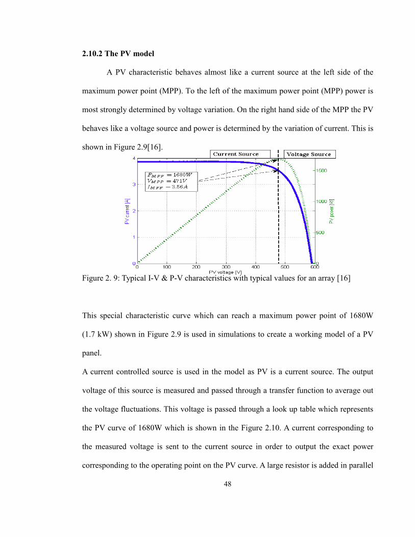
48
2.10.2 The PV model
A PV characteristic behaves almost like a current source at the left side of the
maximum power point (MPP). To the left of the maximum power point (MPP) power is
most strongly determined by voltage variation. On the right hand side of the MPP the PV
behaves like a voltage source and power is determined by the variation of current. This is
shown in Figure 2.9[16].
Figure 2. 9: Typical I-V & P-V characteristics with typical values for an array [16]
This special characteristic curve which can reach a maximum power point of 1680W
(1.7 kW) shown in Figure 2.9 is used in simulations to create a working model of a PV
panel.
A current controlled source is used in the model as PV is a current source. The output
voltage of this source is measured and passed through a transfer function to average out
the voltage fluctuations. This voltage is passed through a look up table which represents
the PV curve of 1680W which is shown in the Figure 2.10. A current corresponding to
the measured voltage is sent to the current source in order to output the exact power
corresponding to the operating point on the PV curve. A large resistor is added in parallel

49
to run the simulation without which algebraic problems occur. A few different PV curves
including 1680W, 3400W and 6800W have been developed for simulation purposes.
Figure 2. 10: PV model designed in Simulink.
2.10.3 MPPT control block
The MPPT block shown in Figure 2.11 is an Embedded Matlab Function designed to
track the operating point by measuring the output power from the PV model. The simple
Perturb and Observe (P&O is discussed in detail in Sections 4.1 and 4.2 of Chapter 4)
algorithm shows how the block observes the change in power and moves the operating
point on the curve by moving in the direction of increased power. The algorithm shown
in Figure 2.11 senses the instantaneous power (u) and compares it with the previous
value (Pold) in order to decide the change in duty cycle reference (y1) with steps of 0.1.
The output of the MPPT block is a reference to generate the required duty cycle (PWM
pulse) which is used to operate the dc-dc boost circuit.

50
y1=dc-dc boost duty cycle reference
u=PV power input
function [y1,Pold1] = MPPT(u,Pold,y)
% This block supports an embeddable
subset of the MATLAB language.
% See the help menu for details.
if (u>Pold)
inc=1;
else
inc=-1;
end
ref = y +0.1*inc;
if (ref>6)
ref=6;
else if (ref<-6)
ref=-6;
end
end
Pold1=u;
y1=ref;
Figure 2. 11: The design of MPPT block

51
2.10.4 Design of dc-dc boost circuit
The dc-dc converter in the photovoltaic system (shown in Figure 2.12) is used to convert
the dc electrical energy from the solar panel into a stable and reliable dc power source
for use by the load or transfer energy to the grid. The dc-dc converter will also provide
impedance matching for maximum power transfer.
Figure 2. 12: DC-DC boost circuit model for simulation
The 1.7 kW and 3.4 kW PV curves created in Section 2.10.2 are used in the simulation
of the PV grid connected system. A dc link of 780V is maintained to generate 325V ac
pk, 50 Hz sinusoidal voltage at the inverter output terminals with a modulation index of
0.8.

52
Inductor and capacitor calculation for the power curves of 1.7 kW and 3.4 kW are as
follows.
DC current flowing out of the dc-dc boost circuit for the two PV curves are:
A 2.15 780V
kW 1.7= and A 36.4
780V
kW 3.4=
Resistance seen by the boost circuit = 362 2.15A
780VΩ= and 179
4.36A
780VΩ=
If 400V input is considered and 780V is required output, d (duty cycle) required is 49%
using (2.19): DV
V
i
o
−=
1
1 (2. 19)
To calculate the required inductor, L and capacitor, C values, the following two
equations from [25], [43] are required:
f
DRDL
2
)1( 2−= (2. 20)
RfV
DVC
r
out= (2. 21)
Where: D is the duty cycle, f is frequency of the switching PWM, 0V is the dc link
voltage, rV is the dc link voltage ripple and R is the resistance of the load seen by the
boost converter.
The equations (2.20) and (2.21) give the minimum value of the L and C respectively,
which is required for safe operation in continuous conduction mode.
According to the equations (2.20) and (2.21), once D is fixed, the value of L and C will
depend on R and f. Once f is decided, the L value is proportional to R and the C value is

53
inversely proportional to R. The L and C values are chosen such that the converter can
operate at both the power levels efficiently. Therefore, according to the required D value
of 49%, R = 362Ω is used for choosing L and R=179 Ω is used for choosing C. Two
frequency scenarios were simulated.
(a) Low frequency PWM for running the simulation faster:
Inverter PWM frequency = 2 kHz
Simulink sampling frequency / step size = 125 kHz / 8µs
dc-dc boost PWM frequency = 2 kHz
Therefore required L≈33mH using (2.20) and C≈68µF using (2.21) with 2% voltage
ripple.
(b) High frequency PWM for running the simulation with real small sized L and
C
Inverter PWM Frequency = 20 kHz
Simulink sampling frequency/ step size = 1250 kHz / 800ns
dc-dc boost PWM frequency = 20 kHz
Therefore required 3.4mH ≈L and F7µ≈C using (2.20) and (2.21) respectively.

54
2.10.5 Model of PWM inverter
Figure 2.13 shows the inverter block in Simulink used for simulation purposes along
with its property window.
Figure 2. 13: 3-leg inverter block and its properties
2.10.6 Model of LCL filter
A low pass filter is used to retrieve the fundamental sine wave from the PWM output of
the inverter block. A compromise is made between the values of L and C, to reduce the
absorption of current by the filter and have a lower cut-off, which in turn would also
reduce the physical size of the components (mainly inductor size).
The cut of frequency of the filter can be defined asCLL
LLf
⋅⋅
+=
π21
(2. 22)
Section 5.1.7 and 5.1.8 discuss the inductor and capacitor values chosen for the final
hardware prototype, which are also used in simulation. For the setup, L=7.5mH (0.6Ω)

55
and C=10µF has been used for which the cut off frequency, f=851 Hz allows the
fundamental and up to seventeen harmonics of the inverter voltage to enter the grid.
Figure 2.14(a) shows the LC part of the filter which is connected to the series RL branch
(0.6Ω,7.5mH) in order to model the LCL filter (see Appendix 1).
Figure 2.14(b) shows the transconductance response against the frequency for the LCL
filter that was simulated in LT Spice. It clearly shows that the 50Hz components pass
through the filter and it behaves mainly as an inductor within the region of interest. 20
kHz PWM components are well attenuated and the cut off frequency is close to 850Hz.
(a) Model of LCL and LC filter subsystem
(b) Transconductance response (I[Vg]/V[Vinv])
Figure 2. 14: Selection of LCL filter values

56
2.10.7 Coupling impedance
The coupling impedance between the inverter and the grid is the impedance of the LCL
filter as shown in Figure 1.1, across which the inverter voltage is displaced to transfer the
required ac current. If the impedance of the capacitor (10µF) is ignored, the impedance
of the two inductors (0.6Ω, 7.5mH) in series comes into effect as the coupling
impedance (i.e. 71.7586.4 ∠=Z for 50 Hz).
2.10.8 DC link controller
The dc link controller algorithm shown below maintains the dc link voltage at 780V
during the simulation and outputs the ac current reference that is used to inject power
into the grid (see Figures 2.17 to 2.19).
function Iref = DC_Link_controller(Vcap,Iref_old)
% This block supports an embeddable subset of the MATLAB language.
% See the help menu for details.
if (Vcap>780)
inc=1;
else if(Vcap<779)
inc=-1;
else
inc=0;
end
end
ref = Iref_old +(0.01*inc);
if (ref>15)
ref=15;
else if (ref<0)
ref=0;

57
end
end
Iref=ref;
2.10.9 List of simulations carried out
The following simulations (a) to (f) were performed in modules to study and develop the
final grid connected photovoltaic inverter system simulation models (g) to (i).
a) SPWM and SVPWM generation
b) Voltage source inverter control using SPWM
c) Z-Source inverter control using SPWM, with simple shoot-through control
d) PV model is run with a variable resistor to see how the operating point on the
power curve moves
e) Boost circuit and three-phase inverter interaction using a fixed dc source
f) Boost and MPPT algorithm with three-phase inverter supplying a standalone load
g) Full three-phase grid connected inverter system with: PV (1.7kW and 3.4kW),
boost, MPPT, three-phase inverter and grid where full control program in Figure
2.15 is applied. (see Appendix 1 for the full Simulink model)
h) Islanding situation is simulated during the worst case, where the supply of
generator and load matches (three-phase load of 3.2 kW is used). Simulation is
carried out with 1.7kW and 3.4 kW PV curves, where the load is almost matched
with the 3.4kW PV curve.
i) Islanding situation with large mismatch of power (5 kW load and the above two
PV curves are simulated)

58
2.11 Control program
The flowchart shown in Figure 2.15 describes the full control program algorithm for the
last three simulation models (g, h, i) mentioned in Section 2.10.9. The following steps
are carried out at fixed Simulink sampling frequencies described in Section 2.10.4:
• Three-phase grid voltages (Va ,Vb,Vc) at PCC, PV operating voltage (VPV), dc
link voltage (Vdc), and PV operating current (IPV) are continuously acquired.
• The RMS and peak value )2*(RMS of these sampled grid voltages are
calculated.
• The sensed grid signals are divided by the fixed peak value to get a sinusoidal
normalised to 1V Pk-Pk, which is the normalised grid voltage signal. Any
voltage distortion, sag or swell would directly be reflected on the normalised grid
signal with this process.
• Positive sequence component is retrieved for the above three-phase voltage
signals which go through a three-phase discrete PLL.
• The PLL is then used to retrieve the frequency and phase information ( tω ) of this
normalised grid voltage signals.
• The RMS of the three grid voltages, along with the Iref (inverter ac current
reference which is generated by the dc link controller), Vdc and Z (value of
coupling impedance of the LCL filter) are used to calculate the Vinv Pk (required
inverter peak voltage) and δ (lead angle) continuously, using the power flow
theory discussed earlier in Chapter 2.
• The Vdc is sensed simultaneously. The M (modulation index) is calculated using
Vdc to produce the required Vinv .

59
• Vinv, δ and M along with the tω information is used to generate three sinusoidal
reference signals for generation of three PWM pulses at 20k Hz using SPWM.
• The three PWM pulses switch the three top switches of the inverter block.
Inverted sinusoidal references are used to generate three inverted 20 kHz
switching pulses that switch the three bottom switches.
DC link controller
The dc link controller runs in parallel to the above steps, which is based on a
programmed embedded Matlab script. It keeps the dc link voltage maintained at 780V by
controlling the refI accordingly. If the dc link voltage below 779V is sensed, refI is
decreased and if voltage above 780V is sensed then the refI is increased. This step size
for increment and decrement is carefully chosen in order to keep up with the 250 Hz
sampling frequency of the dc link controller. Algorithm shown in Section 2.10.8.
MPPT Controller
The MPPT controller is also based on an embedded Matlab script which runs in parallel
by calculating the instantaneous PVP and perturbing the duty cycle of the dc-dc boost
converter as explained in Section 2.10.3. The controller is run at only 50Hz as MPPT is
run at much lower speeds compared to the dc link controller and the main program.

60
Figure 2. 15: Control program used for simulation of grid connected PV inverter

61
2.12 Simulation and results
This section shows only the simulation results obtained from the basic grid connected
inverter control. Two PV curves 1.7kW and 3.4kW are used to supply power to the 400V
L-L three-phase grid and 400V L-L three-phase load. The P&O MPPT algorithm
extracts maximum power from the PV source at all times by controlling the boost duty
cycle. The power fed into the dc link capacitor is transferred to the grid, using the current
reference that is generated by the dc link controller. The dc link controller maintains the
dc link voltage close to 780V with a 2% ripple (this dc link voltage is required to
produce 325V ac pk, M=0.8 during synchronization, M is increased accordingly to
transfer the available power). The flow chart of the full control program with description
is given in Section 2.11.The three-phase load of 3.2 kW absorbs active power at the PCC
at all times. The simulation is run with the 1.7kW PV curve until 0.1s and automatically
shifted to the 3.4kW PV curve till the end of simulation. This is done to verify that the
MPPT algorithm works at different power levels i.e. with different panel output power
levels and extreme variation in insolation.
At this stage no islanding protection (passive or active) is incorporated in the inverter
and two main cases were simulated:
Case 1: the PV generation closely matches the load
Case 2: large mismatch of power
Islanding protection is incorporated and will be seen in Chapter 6 of this thesis.

62
Case 1
During the first 0.1s period, the PV source can only supply 1.7kW of power and the
remaining power required by the load is delivered by the grid. After 0.1s the PV can
supply all the power required by the load and the grid is expected to play no part in
delivering power (matched power situation or we can call it very little mismatch of
power). The grid is disconnected at 0.4s by opening the breaker (SW1) at the grid side
and the system experiences islanding with matched power between the source and the
load. The expected inverter voltage, grid voltage, inverter current, load current, grid
current and dc link voltage are retrieved using Simulink scopes and sent to Matlab
workspace, which are used for plots below. Photovoltaic power transferred into the grid
and the maximum power point tracking capability of the conventionally adopted P&O
method are presented. Figure 2.16(a) shows the tracked tω information with respect to
the normalized grid voltage. Figure 2.16(b) shows the frequency tracked by the three-
phase software PLL. Figure 2.17 shows the dc link voltage maintained throughout the
simulation time. Inverter dc link controller controls the Iref to keep the Vcap to 780V as
close as possible. This controlled current reference depends on the Vcap and is shown in
Figure 2.18. Figure 2.19 shows the extracted PV power. Figure 2.20 shows the PV
operating voltage and Figure 2.21 shows PV operating current against time. Figure 2.22
shows the inverter line voltage, phase voltage and inverter output current. Figure 2.23
presents the grid voltage and the injected grid current. Figure 2.24 shows the inverter
output current, grid current, load current and load voltage before and after islanding.
Results of simulation in Figure 2.24 clearly show the grid is supplying the balance of
power (2.3 A rms) until 0.1s and then the grid current goes towards zero as the 3.4 kW

63
PV is capable of fully powering the load (3.2 kW) after 0.27s (when Iref reaches the
maximum). At 0.4s the grid fails and the grid current goes to zero while the inverter
current (4.6 A rms) stays the same providing the load (islanded). The load current (4.6 A
rms) remains almost unchanged throughout the period. No appreciable change in load
voltage profile is observed with this matching power case.
Case 2
The simulation is again carried out with a large three-phase load (5 kW, 7.3A rms
required per phase) connected to the existing system model. Figures 2.25 and 2.26 show
the simulation results of an islanding scenario with large mismatch of power between the
PV source (3.4 kW) and the load after islanding.
Figure 2.25 gives the frequency at PCC. It shows that the frequency goes down after
islanding at 0.4s due to large mismatch of power.
Figure 2.26 presents the inverter output current, grid current, load current and load
voltage before and after islanding. It shows that before 0.1s the inverter provides little
current (only 2.3A rms is expected of 1.7kW PV) and the grid supplies the rest (5 A
rms). After 0.1s the power from the PV has increased (4.6A rms expected of 3.4 kW PV,
Iref reaches the maximum at around 0.23s) thus reducing the current from grid. After
0.4s, the grid has failed and inverter tries to provide all the power to the load (5 kW)
even though it is not capable (PV can provide only 4.6A of the 7.3A rms required),
hence the PCC voltage and frequency start to drop.

64
0 0.05 0.1 0.15 0.2 0.25 0.3 0.35 0.4 0.45
-1
0
1
2
4
6
8
Time(s)
Vo
lta
ge
(V)
normalized grid voltage phase 'A'
w t
0 0.05 0.1 0.15 0.2 0.25 0.3 0.35 0.4 0.4549.7
49.8
49.9
50
50.1
50.2
Time(s)
Fre
qu
en
cy
(Hz
)
1.7 kW PV 3.4 kW PV Grid connected Islanded
All plots clearly indicate the three different periods occurring:
• 1.7kW PV in grid connected mode till 0.1s
• 3.4kW PV in grid connected mode from 0.1s till the end of simulation
• Islanded at 0.4s
The results above show that the MPPT algorithm works well tracking the MPP at all
times. The dc link controller works well maintaining the dc link voltage and generating
an ac current reference as expected. The system runs as expected producing satisfactory
results leading to the construction of hardware prototype which is looked at, in Chapter
5.
Chapter 3 (detailing the boost), Chapter 4 (detailing the MPPT) and Chapter 6 (detailing
the anti-islanding) include their own detailed simulation results.
(a)
(b)
Figure 2. 16: PLL tracking capability

65
0 0.05 0.1 0.15 0.2 0.25 0.3 0.35 0.4 0.45778
780
782
Time(s)
dc
lin
k v
olt
ag
e(V
)
1.7 kW PV 3.4 kW PV Grid connected Islanded
Figure 2. 17: Vcap maintained at 780V
0 0.05 0.1 0.15 0.2 0.25 0.3 0.35 0.4 0.450
1
2
3
4
5
Time(s)
Cu
rre
nt
refe
ren
ce
(A)
Grid connected Islanded1.7 kW PV 3.4 kW PV
Figure 2. 18: Iref changed according to the available power
0 0.05 0.1 0.15 0.2 0.25 0.3 0.35 0.4 0.450
500
1000
1500
2000
2500
3000
3500
Time(s)
PV
Po
we
r(W
)
1.7 kW PV 3.4 kW PV Grid connected Islanded
Figure 2. 19: Power from PV extracted at MPP, tracked using the MPPT algorithm

66
0 0.05 0.1 0.15 0.2 0.25 0.3 0.35 0.4 0.450
100
200
300
400
Time(s)
Vp
v(V
)
1.7 kW PV 3.4 kW PV Grid connected Islanded
Figure 2. 20: Operating Vpv against time
0 0.05 0.1 0.15 0.2 0.25 0.3 0.35 0.4 0.450
2
4
6
8
Time(s)
Ipv
(A)
1.7 kW PV 3.4 kW PV Grid connected Islanded
Figure 2. 21: Operating Ipv against time
0 0.05 0.1 0.15 0.2 0.25 0.3 0.35 0.4 0.45
-600
-400
-200
0
200
400
600
Time(s)
Vo
lta
ge
(V)
/ C
urr
en
t*1
0(A
)
Vinv LL
Iinv*10
Vinv L-N
1.7 kW PV 3.4 kW PV Grid connected Islanded
Figure 2. 22: Inverter voltage and current

67
0 0.05 0.1 0.15 0.2 0.25 0.3 0.35 0.4 0.45-400
-200
0
200
400
Time(s)
Gri
d v
olt
ag
e(V
) /
Gri
d c
urr
en
t*1
0(A
)
Vg
Ig*10
1.7 kW PV Grid connected Islanded3.4 kW PV
Figure 2. 23: Grid voltage and injected grid current
0 0.05 0.1 0.15 0.2 0.25 0.3 0.35 0.4 0.45
-5
0
5
Inv
ert
er
cu
rre
nt
(A)
0 0.05 0.1 0.15 0.2 0.25 0.3 0.35 0.4 0.45
-5
0
5
Gri
d c
urr
en
t(A
)
0 0.05 0.1 0.15 0.2 0.25 0.3 0.35 0.4 0.45
-5
0
5
Lo
ad
cu
rre
nt(
A)
Load 3.2 kW
0 0.05 0.1 0.15 0.2 0.25 0.3 0.35 0.4 0.45
-325
0
325
Time(s)
Lo
ad
vo
lta
ge
(V)
Grid connected Islanded3.4 kW PV1.7 kW PV
Figure 2. 24: PV inverter and grid together supply power to the load until islanded at
0.4s.
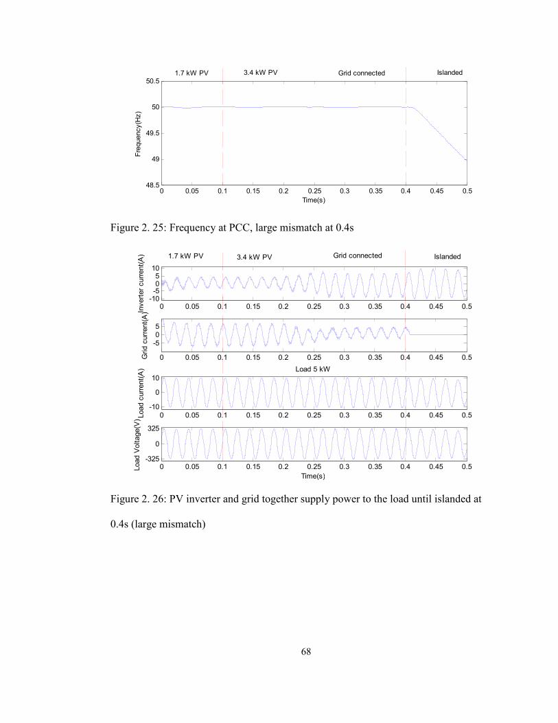
68
0 0.05 0.1 0.15 0.2 0.25 0.3 0.35 0.4 0.45 0.548.5
49
49.5
50
50.5
Time(s)
Fre
qu
en
cy
(Hz
)
Grid connected1.7 kW PV 3.4 kW PV Islanded
Figure 2. 25: Frequency at PCC, large mismatch at 0.4s
0 0.05 0.1 0.15 0.2 0.25 0.3 0.35 0.4 0.45 0.5-10
-505
10
Inv
ert
er
cu
rre
nt(
A)
0 0.05 0.1 0.15 0.2 0.25 0.3 0.35 0.4 0.45 0.5
-505
Gri
d c
urr
en
t(A
)
0 0.05 0.1 0.15 0.2 0.25 0.3 0.35 0.4 0.45 0.5-10
0
10
Lo
ad
cu
rre
nt(
A) Load 5 kW
0 0.05 0.1 0.15 0.2 0.25 0.3 0.35 0.4 0.45 0.5-325
0
325
Time(s)
Lo
ad
Vo
lta
ge
(V)
1.7 kW PV 3.4 kW PV Grid connected Islanded
Figure 2. 26: PV inverter and grid together supply power to the load until islanded at
0.4s (large mismatch)

69
2.13 DSP
Implementation of power electronic converters traditionally employs analogue control.
Lower cost compared to DSP based control was seen as a major advantage in the past.
Despite the cost competitiveness, analog control has many drawbacks such as, the
number of component counts and connections, long-term component instability (aging)
and thermal drift. These adverse effects directly degrade the performance of converters
and cause expensive routine maintenance. In addition, analogue control is typically
designed specifically for a single converter model. As a result, converter upgrade and
scalability are impossible without replacing it with new hardware. Currently, the price of
a single DSP chip has fallen substantially to a few Euros but its performance and
capability of executing millions of instructions (MIPS) is significantly increased.
Two DSP boards are available in the laboratory. Figure 2.27 shows the block diagram of
one of the available DSP controller’s, TMS320F2812 from Texas Instruments. It has a
16 bit fixed-point DSP core which is integrated with several specific peripherals on-chip
including – 2 general purpose timers and 8 PWM generators, 3 capture units, 16
channels 10 bit ADC, CAN interface, SPI, SCI etc. Integration of a high speed DSP core
with specific peripherals not only simplifies the design process but also offers flexibility
via programmability. Thus, advanced control algorithms can be implemented and
upgraded by a short period of development time.

70
Figure 2. 27: Block diagram of Texas Instrument DSP controller TMS320F2812
Figure 2.28 shows the block diagram of the second DSP controller, DS1104 from
dSpace. The DS1104 R&D controller board is a standard board that can be plugged into
the PCI slot of a PC. The DS1104 is specifically designed for the development of high-
speed multivariable digital controllers and real-time simulations which suited our grid
connected inverter application. It is a complete real-time control system based on a 603

71
PowerPC floating point processor (better precision compared to the previous one)
running at a 250 MHz (much faster compared to the previous one). For advanced I/O
purposes the board includes a slave-DSP subsystem based on the TMS320F240 DSP
microcontroller.
The controller board comes with a connector panel CP1104 which provides easy access
to all the input and output signals of the DS1104 controller board. Devices can be
individually connected, disconnected or interchanged without soldering via BNC
connectors and Sub-D connectors. This simplifies some parts of the additional hardware
circuitry that needs to be designed in order for safe usage of the DSP controller.
Figure 2. 28: Block diagram of the dSPace DSP controller DS1104

72
2.13.1 Choice of DSP
While the DIT engineering research team had prior experience with the TM320F2812
the dSpace DSP had not yet been explored prior to this project. This gave an opportunity
to explore its peripherals and capabilities and to choose which one would suit best for the
project.
A detailed study was carried out on both the controller boards with special emphasis
being given to their peripherals like Analog to Digital Converters (ADC), Timers,
General Purpose Input/Output (GPIO), Event Managers (EVA and EVB), Interrupts
system and Pulse Width Modulation (PWM) output channels.
Programming with both the controller boards was practiced, Code Composer Studio for
the TMS320F2812 board and Simulink and Control Desk for DS1104 dSPace board.
Programming with dSPace would take very little time compared to TMS (reduces design
time) as many readily available blocks from Simulink and dSpace (shown in Appendix
7) could be used to build the software.
The DSP controller DS1104 from dSpace was chosen for this project as this controller
could reduce the programming design time. Simulink programs could be run on this DSP
controller via the Real-Time Workshop feature, which means it reduces the development
time greatly. The chosen processor is a floating point processor for higher precision and
a faster processor compared to TMS320F2812.
Simple programs were tested initially to read data into the controller via the ADC and
simple PWM output (with and without dead time) were analyzed on the oscilloscope to
confirm the correct operation of hardware and software. Signals used for control and
monitoring will be received by the DSP after it is conditioned by the measurement

73
interface cards in order for the outside world to interact with the DSP controller safely. A
few measurement interface circuits including the PWM level shifter that drives the
inverter and the boost gate have been designed and built. They are discussed in detail
within the hardware section under Chapter 5 of this thesis.
2.14 Conclusion
This Chapter contained most of the sections that cover the background and literature
study required to achieve the goals stated in Chapter one. It went into details of PV, grid
connected inverter control, power transfer theory, MPPT and generation of PWM. It
also looked into detailed design of the parts that make up the full simulation model such
as PV, dc-dc boost converter, inverter switches, LCL filter etc. The full control program
flow chart is presented with comprehensive description of the steps involved. Results
seen are as expected and agree with the theory in the literature study. The design
complied mainly with the EN50438 standard and also was in agreement with some of
others listed. The two DSP boards available were discussed and the chosen board was
justified. Literature review related to boost topology, MPPT and anti islanding is detailed
in Chapter 3, 4 and 6, respectively.

74
Chapter 3
3. TOPOLOGY COMPARISON BETWEEN Z-SOURCE INVERTER
AND DC-DC BOOST WITH VOLTAGE SOURCE INVERTER
3.0 Introduction
A comparative review of VSI (voltage source inverter) with dc-dc boost and a ZSI (Z-
source inverter) was done to choose the topology to be used in implementation of the
final design of the laboratory prototype. Some papers suggest that that ZSI could
increase the efficiency of the inverter by a few percent, while some argue the difference
is not much [26]-[29]. A detailed comparison of VSI with dc-dc boost to ZSI is given in
this Chapter and the choice of boost topology employed for final design is discussed.
3.1 Boost converter
As dc-dc boost converter is a well known dc voltage step up converter (shown in Figure
3.1 (a)), only a brief description is given in this section. The dc-dc boost circuit design in
Chapter 2 and 5, operates in continuous conduction mode. When the boost converter
operates in continuous conduction mode, the inductor current (IL) never falls to zero.
Figure 3.2 shows the typical voltage and current waveforms of a boost converter
operating in the continuous conduction mode. Assuming components with ideal behavior
operating in steady state conditions, the two operating modes, ‘On state’ and ‘Off state’
are as follows.

75
During the On-state, the switch S is closed as shown in Figure 3.1 (b) and the input dc
voltage (Vi) appears across the inductor, which causes a change in current (IL) flowing
through the inductor during a time period (t) by the equation:
L
V
t
I iL =∆∆
(3. 1)
At the end of the On-state, the increase of IL is therefore:
∫ ==∆DT
iionL VL
DTdtV
LI
0
.
1 (3. 2)
Where, D is the duty cycle. It represents the fraction of the commutation period T during
which the switch is on. Therefore, D ranges between 0 (S is never on) and 1 (S is
always on).
During the Off-state, the switch S is open as shown in Figure 3.1 (b), so the inductor
current flows through the load. If we consider zero voltage drop across the diode, and the
capacitor is large enough for its voltage to remain constant, the evolution of LI is:
dt
dILVV L
oi =− (3. 3)
Therefore, the variation of LI during the Off-period is:
L
TDVV
L
dtVVI oi
TD
oioffL
)1)(()()1(
0
.
−−=
−=∆ ∫
−
(3. 4)
Substituting (3.2) and (3.4) into 0.. =∆+∆ offLonL II we get:
DV
V
i
o
−=
1
1 (3.5)
From the above expression (3.5) it can be seen that the output voltage is always higher
than the input voltage (as the duty cycle goes from 0 to 1), and that it increases with D ,
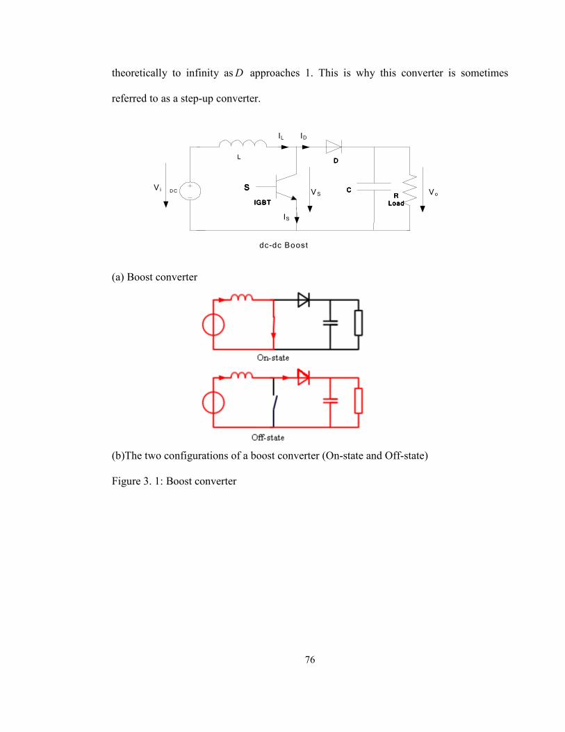
76
dc-dc Boost
SSSS CCCC
L
DC
DDDD
IGBTIGBTIGBTIGBTR R R R
LoadLoadLoadLoad
IL ID
IS
V i VS Vo
theoretically to infinity as D approaches 1. This is why this converter is sometimes
referred to as a step-up converter.
(a) Boost converter
(b)The two configurations of a boost converter (On-state and Off-state)
Figure 3. 1: Boost converter

77
Figure 3. 2: Waveforms of current and voltage in a boost converter operating in
continuous mode.
3.1.1 Choice of capacitor and inductor
The choice of inductor and capacitor values for the dc-dc boost converter can be made
using (3.6) and (3.7), respectively [25], [43]. The equations below give the minimum
value of the L and C required for safe operation in continuous conduction mode.
f
DRDL
2
)1( 2−= (3.6)
RfV
DVC
r
o= (3.7)
Where: D is the duty cycle, f is frequency of the switching PWM, 0V is the dc link
voltage, rV is the dc link voltage ripple and R is the resistance of the load seen by the
boost converter.

78
3.2 Z-Source inverter
The ZSI has a unique impedance network with two split inductors and two
capacitors in X- shape, as shown in Figure 3.3. The three-phase ZSI bridge has nine
permissible switching states unlike the traditional VSI that has eight switching states.
The ZSI has six active states when the dc voltage is impressed across the three-phase
load, and two zero states when the load terminals are shorted through either the lower or
upper three switching devices, respectively. The ninth state, the ST state (shoot-through
state) occurs when the load terminals are shorted by both the upper and lower switching
devices of any phase leg (this state is forbidden in the traditional inverters to avoid ST
fault). This ST state sometimes also called the ‘third zero state’, can be achieved by
seven different ways: ST via any phase, combinations of any two phase legs and all three
phase legs [30]-[32]. Since the ZSI uses the traditional eight states as in traditional
inverters with an extra state, the traditional PWM techniques (Sine PWM and Space
Vector PWM) can be used with slight modification to the zero states. The ST states are
inserted only into the zero states while the active states remain unchanged and hence the
ac output voltage of the inverter remains similar to a traditional inverter. The ST states
are limited by the zero states and may replace some or all of them depending on the
modulation index, M . This shoot-through zero state gives a unique buck-boost feature to
the inverter, which makes it distinct from a traditional VSI or CSI [26]-[39].
The Z-network is responsible for boosting and also tracking the MPP. The shoot-through
duty cycle T0/T [31], can be increased or decreased depending on the change in power
absorbed by the inverter from the dc source (P&O Method). This process is identical to

79
MPP tracking in the traditional VSI with dc-dc boost topology. The duty cycle at MPP,
absorbs all the power from the PV panel hence matching the PV panel with the ZSI.
Figure 3. 3: General configuration of a ZSI [30]
3.2.1 Z-Source inverter operation
Depending on the switching states of the inverter bridge, the ZSI can be classified into
three operation modes as given below:
Mode 1: Inverter bridge is operating in one of the six active states and the bridge can be
seen as an equivalent current source as shown in Figure 3.4(i). During this mode the dc
source voltage appears across the ‘inductor and the capacitor’. Capacitor is charged
(stays charged at steady state) and energy flows to the load via the inductor.
Mode 2: Inverter bridge is operating in one of the two zero states as the bridge ‘short-
circuits’ the load through either the upper or lower three switching devices. During this
mode the bridge can be viewed as an ‘open-circuit’ (current source with zero current
flowing, shown on Figure 3.4 (i)). Voltage of the dc source appears across the ‘inductor
and the capacitor’, except that no current flows to the load, from the dc source.
Mode 3: Inverter Bridge is operating in one of the seven different ways of ST. The
bridge is viewed as a ‘short-circuit’ from the dc link of the inverter as shown in Figure
3.4 (ii). During this mode, no voltage appears across the load like in the zero state

80
operation, the dc voltage of the capacitor is boosted to the required value according to
the ST duty ratio. This ST interval ( 0T ) is inserted into the zero states to boost the
voltage whenever the PV panel is unable to provide the required voltage or during any
voltage dips due to the changing insolation (irradiance) and temperature. While in this
mode the dc source (PV) is separated from the inverter bridge by the diode ( dV > PVV , dV
= cV2 ) and the voltages across 1C and 2C appear across 1L and 2L respectively causing
the inductor currents to ramp up. It is noted that the diode conducts in both modes 1 and
2 (non Shoot-through (non-ST)) while it is reversed biased during mode 3 (ST).
(I) (II)
Figure 3. 4: Equivalent circuits of ZSI: (I) Non–Shoot-through mode (II) Shoot-through
mode [31]

81
3.2.2 ZSI circuit equations
Assuming inductors 1L and 2L and capacitors 1C and 2C have the same value
( LLL == 21 and CCC == 21 ), respectively, we can write the voltage equations of ZSI
as:
LLL VVV == 21
CCC VVV == 21 (3.8)
During mode 3 (ST, T0 time interval):
V V CL =
V2 V Cd = (3.9)
0 VPN = (ST)
PNV is PV output voltage or input to the ZSI, VPN is the inverter bridge dc link Voltage
(as shown in Figure 3.4).
During mode 1 and 2 (non-ST, 1T time interval):
CL VV ≠ , VV V V CLPVd +==
PN CCPVL V -V V- V V == (3.10)
PVCL CPN V - 2V V -V V ==
During steady state, average voltage across 0VL1 = over a switching period T
(Where 1T is the non-ST period and 0T is the ST period)
0)(V 10L =−+⋅= TVVTV CPVC
PV
C
V
V=
01
1
T
T
T− (3.11)

82
Average dc link voltage of the inverter bridge:
PNV = T
)V - (2V T 0 * T PVC10 + =
T
)V - (2V T PVC1 = PVVTT
T
01
1
−
From (3.11) PNV = PVVTT
T
01
1
−= CV (3. 12)
Peak dc link voltage during non ST, PVCLCPN VVVVV −=−= 2^
(3. 13)
Substituting VC from (3.11) into (3.13) gives BV V PVPV
01
^
=−
=TT
TVPN (3.14)
Where B is the boosting factor, B =01 TT
T
−=
T
T021
1
− 1≥ (3.15) ( TT =+ 10T )
The output peak phase voltage from the inverter can be expressed as:
2
..
2
.^
^PVPN
ac
VBMVMV == (3.16)
where M is the modulation index ( M 1≤ )
By choosing the appropriate buck-boost factor BMBB ⋅= (0 to infinity) the output
voltage can be stepped up or down.
Capacitor voltage can be expressed as:
From (3.14) we have PVPVPVC V
T
TT
T
VTT
TV
TV
0
0
01
1
01
1
21
1
T
T
T
T
−
−=
−=
−= (3.17)

83
3.2.3 Alternate equations for Z-Source inverter
From equation (3.15) we can derive B
B
T
T
2
10 −= (3.18)
therefore B
B
T
T
2
11 0 +
=− (3.19)
Substituting (3.18), (3.19) into (3.17) we can have capacitor voltage as:
PVPVPVC VB
VBB
BV
T
TT
T
V2
1**
2
1
21
1
0
0
+=
+=
−
−= (3. 20)
Substituting (3.20) into (3.14) we can also have peak dc link at the inverter bridge during
non-ST as:
V1B
2B
1B
2V*BBV C
cPV +
=+
==∧
PNV (3.21)
3.2.4 Z-network component design
3.2.4.1 Inductor calculation
During traditional operation mode (when no boost is involved) the input voltage
appears across the capacitor and no voltage appears across the inductor (only a pure dc
current flows through the inductors). During Z-Source mode (boost is involved) the
inductor should be sized to limit the current ripple. During ST, the inductor current
increases linearly and the voltage across the inductor is same as the voltage across the
capacitor. During non-ST mode (traditional 8 states) the inductor current decreases
linearly and the voltage across the inductor is the difference between the PV input
voltage and the capacitor voltage [33]-[39].

84
The average current through the inductor is: PV
LV
PI = (3.22)
where P is the total power.
Maximum current ripple through the inductors is when maximum ST happens.
Therefore, the peak to peak current ripple of the inductors needs to be decided. A ripple
amplitude of 30% (60 % peak to peak) of the average inductor current is commonly
recommended in the literature [26], [33]. Inductor max current, %30+=∧
LL II
Inductor min Current, %30−=∨
LL II
During ST, VVV CL ==
2
V V V boostedunboosted += or V can be calculated using (3.20)
Inductor value can be calculated using: I
TVL
∆= 0*
(3.23)
Where∨∧
−=∆ LL III ,
T0 is the ST period per switching cycle and can be calculated using
B =01 TT
T
−=
T
T021
1
− and T =
FrequencySwitchingF ,
1
3.2.4.2 Capacitor calculation
The capacitors absorb the input current ripple and provide a stable boosted dc
voltage to the inverter bridge when it is not in ST mode [33]-[35]. Since the dc source

85
and the inverter are both decoupled from the L C section during ST the capacitor must
supply the full inductor current for the duration of the shoot through (T0) (see Figure
3.11). Limiting the capacitor voltage ripple ( CV∆ ) to about 3% at peak power (as
recommended by [26], [33] the capacitor value can be roughly calculated using:
C
L
V
TIC
∆= 0 (3.24)
Where T0 is the ST period per switching cycle, LI is the average current through the
inductor calculated using (3.22), and %3*VVC =∆
3.2.5 Shoot-through (ST) control
Several control methods have been proposed: simple, maximum boost and
maximum constant boost control [36]. Unlike the traditional inverters, the ZSI’s have an
extra ST state during which the output voltage to the load terminal is zero. In order to
maintain the sinusoidal output the active state duty ratio remains unchanged and all or
some of the zero states are turned into ST states.
3.2.5.1 Simple control
In this simple control, two straight lines are used as upper and lower ST reference lines
Vp and Vn respectively, as shown in Figure 3.5. Whenever the triangular waveform is
greater than Vp all the upper switching devices of the inverter are switched “On” while
the lower devices are already “On” causing ST. Similarly ST occurs by turning the lower
switches “On” whenever the line Vn is greater than the triangular waveform. In this
control method the ST duty ratio decreases with increase in M (modulation index) and

86
since all the zero states are not fully utilized, voltage stress on the device is relatively
high as mentioned in [27], [32], and [36].
Figure 3. 5: Sketch map of simple control [36]
3.2.5.2 Maximum boost control
Maximum boost control method is used to obtain the maximum voltage boost. This
control shoots through the entire zero state in a switching cycle, as a result reduces the
voltage stress on the devices. The top contour of all three sinusoids together and bottom
three contours of all three sinusoids together act as the upper and lower ST references
respectively. These references are compared with the triangular waveform to perform the
ST; a control map is shown on Figure 3.6(a). Figure 3.6(b) shows control with third
harmonic injection which gives the advantage of extending the modulation index range.
This method experiences varying ST duty ratio in a line cycle which causes higher
inductor ripple hence requiring high inductance for low frequency or variable-frequency
applications according to [36], [37].

87
Figure 3. 6: Sketch map of maximum boost control [36], [37]
3.2.5.3 Maximum constant boost control
This control method achieves maximum boost while maintaining a constant ST duty
ratio throughout; thus it results in no line frequency current ripple through the inductors.
The PWM control map of maximum constant boost control is shown in Figure 3.7(a) and
map of maximum constant boost control with third harmonic injection is shown in
Figure 3.7(b). Using this method the inverter can buck and boost the voltage from zero to
any desired value smoothly within the limit of the device voltage [36].
(a) Maximum constant boost (b) Maximum constant boost with third harmonic injection
Figure 3. 7: Sketch map of maximum constant boost control [36]

88
For both Figure 3.7(a) and (b) 2
31
M
T
To −= (3.25) according to [36]
Boost factor and voltage gain:
13
1
21
1
0 −=
−=
M
T
TB and
132/ −==
∧
M
MMB
V
V
PV
PN (3.26)
Range of M for Figure 3.7(a) is 3
1 to 1
Range of M for Figure 3.7(b) is 3
1 to
3
2 (increased modulation range)
3.2.6 ZSI self-boost phenomenon
According to [26], simulations reveal that, without the insertion of ST, the ZSI has
a voltage boost when operated at low modulation index and low load power factor.
This can be a problem or an advantage depending on the application. This self boost can
be controlled using a battery in replacement of the second capacitor in the Z network,
2C [26].
While the Z-Source operates in normal mode (non-ST), inductor is assumed to have a
pure dc current flowing through it and the output voltage can be calculated for the
system shown in Figure 3.3,22
3 MVV DC
LL = where LLV is the rms line to line voltage and
== PVDC VV “PV input voltage”.
The total power of the three-phase system is φcos3 LLLL IVP = ,
Calculate inductor current LI :

89
22
cos**3cos**
22
33
21
φφ
LOAD
PV
LOADPV
PV
LLL
IM
V
IMV
V
PIII =
==== (3.27)
Where LLLOAD II = (line to line current) and φcos is the load power factor.
Maximum value of the iI (load current) on Figure 3.8 is equal to the maximum load
current:
Max ( iI ) = LOADI2 (3.28)
iI can also be expressed in terms of dI and LI from Figure 3.8:
dLLdLCLCLi IIIIIIIIII −=−−=−=−= 2)( 112111 (3.29)
Where 21 CC II = and LLL III == 11
Since the current through the diode cannot be negative (lower than 0), the maximum
Li II 2= .
Max ( iI ) = LOADI2 = 2IL = 22
cos**3 φLOADIM*2 =
2
cos**3 φLOADIM (3.30)
However maximum load current can be higher than 2IL when the product of the
modulation index and the load power factor is lower than 2/3 as shown below:
>LOADI22
cos**3 φLOADIM
φcosM <3
2 (3.31)
During this condition the inverter has new operating modes as shown below in Figure
3.8.

90
Figure 3. 8: New operation modes during self-boost [26]
The load current iI is zero during zero states, while during an active state when the
condition in (3.31) is met, the load current iI is larger than what is available ( LI2 ). The
freewheeling diodes Df1 and Df2 are turned on to provide the load with required current,
which in turn puts the inverter into a ST mode as shown in Figure 3.8(a) ( LI increases
linearly at ST until LI2 = required iI , i.e., LI2 is larger)
Then the inverter goes into the active state, where the input diode is still reversed biased
as shown on Figure 3.8(b) and the load current is provided by the capacitor until next
switching action (zero or active state). Voltage is boosted by this unwanted ST (self
boost) [26]. This self boost can be controlled using a battery as explained in [26].

91
3.3 Simulations of VSI (with boost) and ZSI
The boost with VSI and ZSI were both simulated in Simulink. Table 3.1 below gives the
common parameters and the parameters specific to each of the boost converters.
Figure 3.9 shows the results obtained from the simulation of boost with VSI. Figure
3.9(a) shows the load current, Figure 3.9(b) inductor voltage, Figure 3.9(c) inductor
current, Figure 3.9(d) capacitor current, Figure 3.9(e) dc link voltage maintained at 928V
and Figure 3.9(f) load voltage maintained at 230V ac rms. In Figure 3.9: (b) inductor
voltage, (c) inductor current and (d) capacitor current are zoomed in from 0.03s to 0.032s
for better clarity.
Figure 3.10 shows the results obtained from the simulation of ZSI. Figure 3.10(a) shows
load current, 3.10(b) inductor current (IL1), 3.10(c) inductor voltage (VL1), 3.10(d)
capacitor current (IC1), 3.10(e) capacitor voltage (VC1) maintained at 664V as
calculated in Table 3.1, 3.10(f) capacitor voltage (VC2) maintained at 664V, 3.10(g)
inductor voltage (IL2) and 3.10(h) load voltage maintained at 230V ac rms. In Figure
3.10: (b), (c) and (g) are zoomed in from 0.03s to 0.0325s for better clarity.
Figure 3.11 shows the inductor voltage (VL1) and capacitor voltage (VC1) on the same
time axis, it can be noted that during shoot through, difference between the two voltages
is zero.
Figure 3.12(a) shows the dc link voltage of the ZSI and Figure 3.12(b) shows a zoomed
in figure of this dc link voltage from 0.03s to 0.0325s. It is seen that the dc link voltage
is quite pulsating for which reason direct control of dc link is not feasible. Full schematic
diagrams of the two different circuits used for simulations are shown in Appendix 2 and
3.

92
Table 3. 1: Simulation parameters for boost with VSI and ZSI
Simulation parameters for Boost with VSI and ZSI
Power: 1680W, Three-phase load, Phase voltage Vac L-N: 230V rms
Iac phase: 1680W/3 = 560W, 560W/230V = 2.43A rms ( 3.44 A Pk)
Vdc Input for both cases: 400V dc
M=0.7, dc link of inverter required for both cases: 928V
Boost factor required : 2.32
Carrier frequency =10 kHz, Carrier triangle with +10 and -10V Pk-Pk is used
PWM frequency =10 kHz
Boost with VSI ZSI
L> (1-D)2*DR/2f
C> DVo/VrRf
dc side : 1680W/928V=1.81A,
R= 928V/1.81A=512.6Ω
Vo= output voltage (928V), Vr=
capacitor voltage ripple = 27.84V
(3%)
Vout/Vin= 1/1-D
Duty cycle = 57%
Therefore : L= 2.69mH and
C=3.71µF
C
L
V
TIC
∆= 0
I
TVL
∆= 0*
dc side: 1680W/400V= 4.2A
Average inductor is expected to be 4.2A with
60% ripple
Capacitor voltage : 664V with 3% ripple
284.02
10 =−
=B
B
T
T, ST time per cycle
0T = sµ 28.4 , T=1/10 kHz= 100µs.
Therefore: L1=L2=7.48 mH , C1=C2= 5.99 Fµ
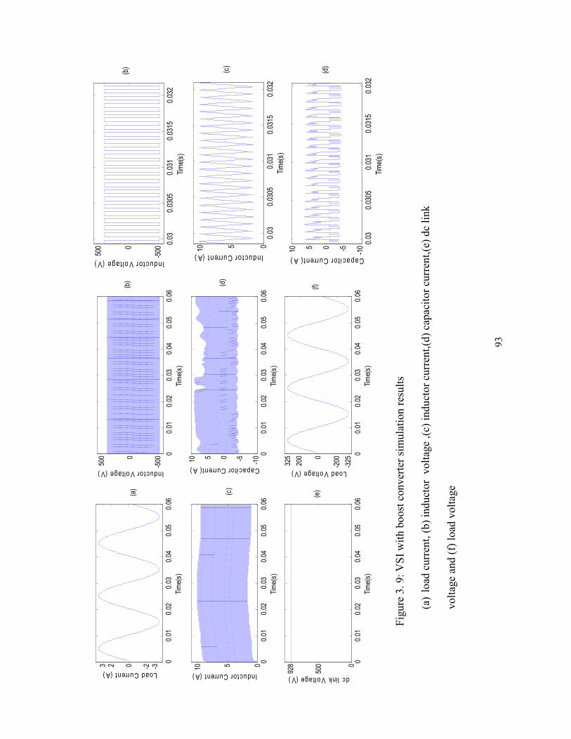
93
Fig
ure
3. 9:
VS
I w
ith b
oost
conver
ter
sim
ula
tion r
esult
s
(a)
load
curr
ent,
(b)
induct
or
volt
age
,(c)
indu
ctor
curr
ent,
(d)
capac
itor
curr
ent,
(e)
dc
link
volt
age
and (
f) l
oad
volt
age
00.
010.
020.
030.
040.
050.
06
-3-2023
Tim
e(s)
Load Current (A)
00.
010.
020.
030.
040.
050.
06
-5000
500
Tim
e(s)
Inductor Voltage (V)0
0.01
0.02
0.03
0.04
0.05
0.06
0510
Tim
e(s)
Inductor Current (A)
00.
010.
020.
030.
040.
050.
06-1
0-50510
Tim
e(s)
Capacitor Current( A)
00.
010.
020.
030.
040.
050.
060
500
928
Tim
e(s)
dc link Voltage (V)
00.
010.
020.
030.
040.
050.
06
-325
-2000
200
325
Tim
e(s)
Load Voltage (V)
(a)
(b) (d)
(c)
(e)
(f)
0.03
0.03
050.
031
0.03
150.
032
-5000
500
Tim
e(s)
Inductor Voltage (V)
0.03
0.03
050.
031
0.03
150.
032
0510
Tim
e(s)
Inductor Current (A)
0.03
0.03
050.
031
0.03
150.
032
-10-50510
Tim
e(s)
Capacitor Current( A)
(b)
(d)
(c)

94
Fig
ure
3. 10 :
ZS
I si
mula
tion r
esult
s
(a)
load
curr
ent,
(b)
L1 c
urr
ent
,(c)
L1 v
olt
age
,(d)
C1
curr
ent,
(e)
C1 v
olt
age,
(f)
C2 v
olt
age,
(g)
L 2
volt
age
and (
h)
load
volt
age
00
.01
0.0
20
.03
0.0
40
.05
0.0
6-4-2024
Tim
e(s
)
Load Current(A)
00
.01
0.0
20
.03
0.0
40
.05
0.0
605
10
Tim
e(s
)
IL1(A)
00
.01
0.0
20
.03
0.0
40
.05
0.0
6
-50
00
50
0
Tim
e(s
)
VL1(V)
00
.01
0.0
20
.03
0.0
40
.05
0.0
6-202
x 1
04
Tim
e(s
)
IC1(A)
Ib:
C1
00
.01
0.0
20
.03
0.0
40
.05
0.0
60
40
0
70
0
Tim
e(s
)
VC1(V)
00
.01
0.0
20
.03
0.0
40
.05
0.0
60
40
0
70
0
Tim
e(s
)
VC2(V)
00
.01
0.0
20
.03
0.0
40
.05
0.0
6
-50
00
50
0
Tim
e(s
)
VL2(V)
00
.01
0.0
20
.03
0.0
40
.05
0.0
6
-32
5-2
000
20
03
25
Tim
e(s
)
Load Voltage(V)
(c)
(e)
(f)
(g)
(h)
(b)
(d)
(a)
0.03
0.03
050
.031
0.03
150.
032
0.0
325
0510
Tim
e(s)
IL1(A)
0.03
0.03
050.
031
0.03
150.
032
0.03
25
-5000
500
Tim
e(s)
VL1(V)
0.03
0.03
050
.031
0.03
150.
032
0.0
325
-5000
500
Tim
e(s)
VL2(V)
(b) (c)
(g)
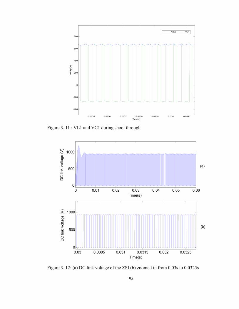
95
0.0335 0.0336 0.0337 0.0338 0.0339 0.034 0.0341
-400
-200
0
200
400
600
800
Time(s)
Vo
lta
ge
(V)
VC1 VL1
0.03 0.0305 0.031 0.0315 0.032 0.0325
0
500
1000
Time(s)
DC
lin
k v
olt
ag
e (
V)
(b)
0 0.01 0.02 0.03 0.04 0.05 0.06
0
500
1000
Time(s)
DC
lin
k v
olt
ag
e (
V)
(a)
Figure 3. 11 : VL1 and VC1 during shoot through
Figure 3. 12: (a) DC link voltage of the ZSI (b) zoomed in from 0.03s to 0.0325s

96
3.4 Comparison of VSI (with boost) and ZSI
Both converter topologies have their own merits and demerits which are compared in the
Table 3.2 below. The output quality from both inverters is comparable, ZSI output
voltage experiences less distortion as no dead bands are incorporated but direct control
of the dc link voltage is complex (see Figure 3.12). Hence, capacitor voltage is usually
employed to retrieve the refI when MPPT algorithm controls the boost factor during grid
connected mode (see section 4.2.3 for further explanation).
Table 3. 2: Merits and demerits between boost with VSI and ZSI
Boost with VSI ZSI
1 large capacitor, 1 large Inductor
1 extra switch which also requires an extra
gate driver circuit
2 small capacitor, 2 small inductors
(slightly large in total) [26]
Traditional Sine PWM used Traditional Sine PWM used with
modification to zero states (shoot through
inserted)
Unwanted shoot through can cause damage
to inverter, dead band needs to be
incorporated
Shoot through deliberately inserted and
causes no damage, can handle unwanted
shoot through
Dead band causes distortion No dead band, no distortion
Efficiency quite high (weighted average
about 90%)
Efficiency comparable at high loads, but
low at low loads due to higher circulating

97
power in Z-source network (weighted
average is slightly lower), efficiency
comparable
Modulation index and Boost factor are not
directly dependent
Modulation Index (M) and Boost factor
(B) are directly dependent on each other, a
higher M, reduces B. This is because the
peak of the modulating wave decides the
minimum value the upper shoot through
reference can take in simple boost control)
No self boost φcosM < 0.67 causes self boost, where
φcos is the displacement factor of the load
Control of dc link voltage is simple dc link voltage is pulsating, direct control
is complex, and hence control of capacitor
voltage is considered.

98
3.5 Choice of boost converter for the hardware prototype
In summary the ZSI offers comparable efficiency to the boost with VSI and only
marginal savings in hardware complexity at the expense of greatly increased control
complexity. The increased control complexity has further impact on a Simulink / dspace
implementation as follows:
Shoot through for a ZSI requires implementation of modified PWM (conventional PWM
merged with shoot-through). The conventional PWM Block available in
Simulink/dSPace (DSP Board) cannot be used to identify the shoot-through ‘insertion
points’. Shoot-through insertion point is the situation where top three switches or bottom
three switches are ‘on’. The dSpace conventional PWM Block requires duty cycle values
as input, to create ‘centred PWM’. This centred PWM output feature cannot be used to
merge the shoot-through with the conventional PWM output (creates unwanted shoot-
through).
Implementing the modified PWM in Simulink is only possible by using a high frequency
carrier, modulating references and two shoot-through references (for top and bottom
switch) per phase as explained in Section 3.2.5.1.
In order to sense the shoot-through points from the high frequency carrier and the shoot-
through references (to obtain shoot-through duty cycle), a much higher sampling
frequency is required. This very high sampling frequency makes the DSP go into an
overrun condition. Nevertheless this method is adopted for only simulation purposes.
This problem is taken as one of the limitation of the existing dSpace DSP software which
has dedicated conventional PWM control blocks only to be used with conventional VSI

99
inverters. For these reasons it was decided to proceed with a dc-dc boost with VSI
topology for this work.
3.6 Conclusion
Two different boost topologies dc-dc boost converter with VSI and ZSI suitable for grid
connected inverter application were investigated in detail. ZSI being a new topology was
analysed in terms of circuit equations, operation modes, control methods and component
design. Simulation results for both the converters were produced in a Simulink
environment and a concluding comparison table was laid down. Choice of boost
converter topology that is used within the prototype was justified with reasons to support
the ease of implementation using the selected dSpace DSP.
100
Chapter 4
4. NEW MAXIMUM POWER POINT TRACKING APPROACH
BASED ON PERTURB AND OBSERVE METHOD
4.0 Introduction
Section 2.1 and 2.2 of Chapter 2 discussed the P-V and I-V characteristics of a PV cell
and the need for a MPPT algorithm. Photovoltaic cells produce a low dc output voltage
which depends on the insolation and the load. Thus, they are unable to connect to the
utility directly. However, they can be interfaced and supply power to the utility by means
of power electronic converters [40]. PV panels are put together in series to achieve a
high output voltage but it is not always feasible to have sufficient panels in series to give
the dc voltage required by the inverter system. Therefore a dc-dc boost circuit is usually
employed to increase the voltage at the inverter dc link. In order to interface with the
nominal 230V Irish (European) low voltage grid the inverter has to produce a peak
voltage of 325V at the ac output terminals.
Adjusting the control of the dc-dc boost front end also allows us to vary the operating
point of the solar cell in order to achieve the maximum power transfer at any given level
of solar insolation. In other words the dc-dc boost circuit is used to acquire the
maximum power out of the PV panels at all times by implementing a maximum power
point tracking (MPPT) algorithm. If a ZSI was used, the ‘boosting stage’ of the circuit is
done by the Z impedance network; the ‘maximum power transfer’ could be controlled by
the shoot-through reference and the inverter ac current (Iref) can be controlled by the dc
link controller.

101
4.1 Maximum power point tracker review
A controller that tracks the maximum power point locus of the PV array is known as a
MPPT controller. There are several algorithms to track the MPP and a few common
maximum power point tracking algorithms have been reviewed. For optimal operation,
the load line must match the PV arrays MPP locus and if the particular load is not using
the maximum power, a power conditioner should be used in between the array and the
load [13],[14],[41].
Figure 4. 1: Basic MPPT system
Figure 4. 2: PV array and load characteristics
Some of the frequently discussed MPPT techniques in the literature are as follows:
• Fractional short circuit current (Isc), a current based MPPT
• Fractional open circuit voltage (Voc), a voltage based MPPT
• Perturb and Observe (P&O) /Hill climbing
• Incremental Conductance Technique (ICT)
• Constant Reference Voltage(CRV)

102
1
* , KMVV vmpp ==
4.1.1 Fractional open circuit voltage/voltage based MPPT technique
This is the one of the most conventional, but it is considered to be a fast, practical and
powerful method for MPP estimation without the need for a powerful DSP. It is based on
the observation that the MPP voltage ( mppV ) can be approximated by a linear function of
the open circuit voltage ( ocV ) [13], [14]. For instance ocvmpp VMV = .
where vM = voltage factor = 0.76 (for instance).
In order to use this method ocV is measured periodically by open circuiting the cell
string. Then, the appropriate mppV can be calculated from a simple voltage divider
( ocvmpp VMV = ). A voltage control loop shown below controls the MPP.
Figure 4. 3: Conventional MPPT controller using open circuit voltage Voc
4.1.2 Perturb and observe (P&O)
This is where the duty cycle (δ ) of the switching converter is periodically increased or
decreased controlling the array power ( P ). The power can be sampled periodically and
compared with its previous value ( 1−− kk pp ). If the power has increased then the δ is
stepped up in the same direction, otherwise δ is stepped in the opposite direction until the
MPP is reached [15]. P&O and the hill climbing method both rely on the gradientdV
dP. If
dV
dP tends to zero or equals to zero then the power is at its maximum point (MPP). If it is

103
positive, then the operating point is on the left of MPP and negative implies the
operating point is at the right of MPP.
This technique could cause power loss when there are very rapid changes in solar
radiation but this is not very common.
4.1.3 Incremental conductance technique (ICT)
MPP can be written as 0=+==dv
divi
dv
dvi
dv
dp
The ICT algorithm checks for v
i
v
i−=
∆∆
by saving previous sampled values bi and bv
i.e., current and voltage values, respectively. The following are calculated, biii −=∆ ,
bvvv −=∆ where i and v are current sample values of current and voltage, respectively.
If v
i
v
i>
∆∆
then the operating point is left of MPP, and v
i
v
i<
∆∆
means the operating point
is right of MPP [14], [15].
The control refV changes depending on this check, it is adjusted to move the array
operating voltage towards the MPP and at MPPv
i
v
i−=
∆∆
. When MPP is reached, the
operation is held at that point refV , unless a change in i∆ is detected. This change will
mean the weather conditions have changed and hence the MPP.

104
4.1.4 Constant reference voltage (CRV)
CRV compares the PV array voltage or current with a constant refV or refI respectively,
which corresponds to photovoltaic V or I at MPP under specific conditions. The error
signal drives the power conditioner that interfaces the PV array to the load.
4.1.5 Discussion of the MPPT control techniques
Incremental conductance is a very good technique for coping with changing atmospheric
conditions contrary to the P&O/CRV, but ICT requires complex mathematical
calculations compared to P&O/CRV [13]-[15]. P&O is quite good but it causes power
losses with rapid solar variation. But with the advancement of DSP’s both ICT and P&O
can be implemented without a problem. CRV is simple to implement but it is not
accurate as different weather conditions with changes in temperature/isolation are not
considered.
4.2 MPPT technique
Perturb and Observe, being the most widely used MPPT technique in literature, was
simulated and analysed in Chapter 2 (see Appendix 1 for the simulation model).
Achieving the maximum power (MPPT control) and control of the voltage dc link are
interconnected, for which reason the control of the inverter current is also discussed.
Maximum power point tracking is done using an algorithm (using P&O method in this
case) that perturbs the duty cycle of the dc-dc boost circuit (see Figure 4.4) and observes
the change in power. The duty cycle is then increased or decreased in the direction of
increasing power [15].
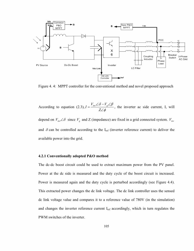
105
Figure 4. 4: MPPT controller for the conventional method and novel proposed approach
According to equation (2.3),φ
βδ
∠
∠−∠=
Z
VVI
ginv, the inverter ac side current, I, will
depend on δ∠invV since gV and Z (impedance) are fixed in a grid connected system. invV
and δ can be controlled according to the Iref (inverter reference current) to deliver the
available power into the grid.
4.2.1 Conventionally adopted P&O method
The dc-dc boost circuit could be used to extract maximum power from the PV panel.
Power at the dc side is measured and the duty cycle of the boost circuit is increased.
Power is measured again and the duty cycle is perturbed accordingly (see Figure 4.4).
This extracted power changes the dc link voltage. The dc link controller uses the sensed
dc link voltage value and compares it to a reference value of 780V (in the simulation)
and changes the inverter reference current Iref accordingly, which in turn regulates the
PWM switches of the inverter.

106
Here the boost circuit extracts the maximum power independently, while the dc link
controller maintains the dc link voltage by controlling the inverter current [16], [42].
Figure 4.5 shows the MPPT controller run at 50Hz to track the power using measured dc
values. Full schematic diagram of the simulation model with conventional P&O MPPT is
shown in Appendix 1
Figure 4. 5: MPPT controller for the conventional method
4.2.2 Novel AC side P&O MPPT technique
DC power at the PV side has always been used in literature for MPP tracking as
discussed above. Power at the ac side has never been considered. In this research study,
power (current) at the ac side could be measured to track the MPP, and the proposed
method takes advantage of this interesting concept which is discussed below.
A sketch of the I-V and P-V characteristic at the PV side and the inverter side is shown
in Figure 4.6.
(a) (b)
Figure 4. 6: Sketch of I-V and P-V characteristic of a PV panel and inverter

107
From Figure 4.6 it can be deduced that for a three phase inverter:
PINV = (PPV –Losses) (4.1)
g
INVINV
V
PI
3/= (4.2)
Where:
PINV is inverter output power
PPV is input PV power
IINV is inverter output current
Vg is grid voltage
The left (PV side) of Figure 4.6(a) shows the usual IPV-VPV and PPV-VPV characteristic of
a PV Panel. This special power curve characteristic is utilized in the conventionally used
P&O MPPT approach to extract the maximum power at the point when 0=dV
dP. When
looking at the ac side (inverter side) as in Figure 4.6(b), the PINV-VPV and IINV-VPV
characteristics seem to be linearly related as shown on the right of Figure 4.6 (losses are
assumed to be fixed). This special I-V characteristic at the ac side can now be used to
track the MPP by measuring the output current of the PV inverter since the grid voltage,
gV , at PCC is constant).
The new concept uses the same P&O MPPT algorithm explained for the conventionally
used MPPT approach, except that it no longer measures the dc power ( dcI and dcV ).
Instead the ac current output is acquired to perturb the duty cycle of the boost circuit as
shown on Figure 4.7. Section 4.2.4 lists the advantages of this approach.

108
Figure 4. 7: MPPT controller for the novel approach
4.2.3 Algorithm for MPPT
AC side current rms (inverter output) is measured and the duty cycle of the boost circuit
is increased. The rms current is measured again and the duty cycle perturbed accordingly
in the direction of increased rms current (power) as shown in the control flow chart in
Figure 4.8. This extracted power changes the dc link voltage. The dc link controller uses
the sensed dc link voltage value and compares it to a reference value of 780V(in this
case) and changes the reference current (inverter side) refI accordingly, which in turn
regulates the PWM switches of the inverter.
Here the inverter side current extracts the maximum power with the use of the boost
circuit, while the dc link controller maintains the dc link voltage by controlling the
inverter current. The boost circuit depends on the inverter output current rms, to control
the MPP. This novel method reduces the dc side sensor requirement for MPP tracking.
See Appendix 4 for a full simulation model.

109
Figure 4. 8 : Control flow chart of the novel P&O MPPT method

110
0 0.02 0.04 0.06 0.08 0.1 0.12500
600
700
780800
time(sec)
Vc
ap
(V)
4.2.4 Advantages of the new MPPT approach
• Only one ac current sensor is required to sense ac inverter current output for
MPPT purpose in a balanced three-phase system.
• No dc sensors required, nor multiplier required to reveal the power in digital
control. This simplifies algorithm and computation.
• Since no voltage (no power) measurement is required, this avoids additional
software filtering for the oscillating PV voltage.
• For a three-phase system, a sensor of smaller rating is required compared to the
conventional method as whole dc power is not measured, instead ac current in
one of the phases (which reflects ac power) is sensed, which is small.
4.3 Simulation results
A PV curve of 3.4kW peak is used to simulate the photovoltaic source. Both the
conventionally used MPPT approach and the novel approach are simulated in Simulink
(tracking MPP at 50Hz) for a three-phase photovoltaic grid connected inverter whose
results are shown below. Simulation models are shown in Appendix 1 and 4. Inverter Vdc
link controller, controls the Iref to keep the capacitor voltage (Vcap) to 780V as close as
possible as shown in Figure 4.9.
Figure 4. 9: Vcap maintained at 780V

111
0 0.02 0.04 0.06 0.08 0.1 0.120
1000
2000
3000
3500
time(sec)
Po
we
r(W
)
0 0.02 0.04 0.06 0.08 0.1 0.120
1000
2000
3000
3500
time(sec)
Po
we
r (W
)
Figures 4.10 and 4.11 show the power extracted using the conventional and novel
approach, respectively. The dc power calculated in Figure 4.10 is used for MPP tracking,
while the dc power shown in Figure 4.11 is just calculated to show that the novel
approach extracts maximum power without any dc sensors.
Figure 4. 10: Power from PV tracked using the MPPT algorithm using the
conventionally used approach.
Figure 4. 11: Power from PV calculated to show the tracked MPP using the novel
approach.

112
0 0.1 0.2 0.3 0.4 0.5 0.6 0.7 0.8 0.9 10
100
200
300
400
500
Time(s)
Vp
v(V
)
0 0.1 0.2 0.3 0.4 0.5 0.6 0.7 0.8 0.9 10
500
1000
1500
2000
2500
3000
3500
Time(s)
Po
we
r(W
)
The simulation is run again with 1.7kW PV and 3.4kW PV, where the switching of the
curve takes place at 0.4s. Figure 4.12 shows the extracted power from the panels using
the novel approach, the power here is calculated only for verification purposes. Figures
4.13 and Figure 4.14 show the operating Vpv and Ipv against time respectively. Figures
2.19 to 2.21 of Chapter 2 showed results of the conventional approach under similar
conditions.
Figure 4. 12: Power from PV calculated to show the tracked MPP using the novel
approach
Figure 4. 13: Vpv operating point against time

113
0 0.1 0.2 0.3 0.4 0.5 0.6 0.7 0.8 0.9 10
1
2
3
4
5
6
7
8
9
Time(s)
Ipv
(A)
Figure 4. 14 Ipv operating point against time
4.4 Conclusion
The Chapter discussed the various MPPT techniques from literature and the need for a
boost circuit to increase the voltage level and MPP tracking. It also discusses the
conventional method for MPPT and then proposes a new ac side P&O MPPT approach.
The new proposed method brings a master-slave principle approach, where the inverter
and the boost circuit are looked at as two different controlling stages. One of them can
act as the master while the other as a slave. Both of them can be used vice versa to
control the overall transfer of maximum power to the grid from a PV source.
Simulation results for both the conventional and novel approach show the working
model of the system. The new proposed approach uses only ac side grid current for
MPPT. The injected grid current is normally sensed in a grid connected system. As a
result the new method does not require any additional dc side measurements, making it a
dc sensor-less MPP tracking approach. Furthermore, no compromises are made in the
power tracking capability (compare Figure 4.10 with 4.11 and 2.19 with 4.12) and
serving some further advantages as mentioned in Section 4.2.4.

114
Chapter 5
5. IMPLEMENTATION OF THE THREE-PHASE GRID
CONNECTED INVERTER: HARDWARE, SOFTWARE AND
CONTROL
5.0 Introduction
Chapters 2 and 3 show simulations of the power electronic systems, and their
significance in the analysis and design of the entire three phase grid connected inverter
system.
However computer simulations cannot be taken as a substitute for a hardware prototype.
Power electronics computer simulation and a hardware prototype are complementary to
each other. A laboratory prototype of a three phase grid connected dc-ac inverter has
been constructed in order to validate the simulated grid connected system and to test the
proposed anti islanding technique. The software control program developed in Simulink
is run on dSpace DSP DS1104.
This Chapter reports the development of the laboratory prototype, the necessary interface
circuits, the software control algorithm and the GUI (graphical user interface) developed.
The Chapter concludes with experiment results of the grid connected inverter system,
interface circuits and a discussion of the interaction between hardware and software.

115
5.1 Implementation of a laboratory prototype
5.1.1 Power circuit configuration and components parameters
A 5.625 kW, 25A, 50 Hz three-phase grid connected inverter with a rectified dc source
was built with the necessary control and protection circuitry. The rectified dc source is
used in place of the PV Panel for experiments. A dc-dc boost converter is incorporated
between the dc source and the inverter. The 400V L-L grid is stepped down to 130V L-L
using a three-phase isolated transformer, so that the minimum boosted dc link voltage
level required to operate the inverter can be set at 265V and the normal controlled
voltage level is set to 300V. The power circuit layout of the grid connected inverter
prototype is shown in Figure 5.1. Figure 5.1 shows the full inverter system along with
the necessary interface ciruits. The three-phase transformer has the capability of stepping
down the 400V L-L to 87V L-L (3.75 kW), 130V L-L (5.625 kW) and 173V L-L
(7.5kW). All components are designed for the full power range of 5.625 kW but
experiments have been carried out only up to 2 kW. Figures in Appendix 6 show the
hardware setup in progress for the project.

116
AC
AC
AC
Rectified
DC Source
Inverter
LCL Filter
SW2
3-Phase
AC Grid 400V
LL
Dc-Dc Boost
3-
Phase
Load
PCC
B BBB
Vdc Link
Vdc Link
Vdc Link
Vdc Link
2200
2200
2200
2200uF uFuFuF
500
500
500
500V VVV
Wavelet Analysis &
Detection of
Islanding situation
Enable (0-10V)
SW1 n
3-Phase
Transformer
400-130 VLL
3 x AC
Voltage
Interface
Circuit
7.5m
H7.5m
H
10uF
250V,
50 Hz
AC
5mH
Vdc Source
Vdc Source
Vdc Source
Vdc Source
2500
2500
2500
2500uF uFuFuF
350
350
350
350V VVV
Vac Source
Vac Source
Vac Source
Vac Source ( (((Triac
Triac
Triac
Triac) )))
230
230
230
230V VVV, ,,,50505050Hz
Hz
Hz
Hz
dSpace
DS1104
Runs @
300V
Runs @
150-300V
CT
CT
CT
CT
CT
CT
CT
CT
CT
CT
CT
CT
3 x AC
Current
Interface
Circuit
Synshronisation
PWM control
Vdc Link Control
Power transfer
Protection
Anti-islanding Protection
2 x DC Voltage
&1 DC Current
Interface Circuit
CT
CT
CT
CT
16A
current
protection
X 6
0-5V
PWM Level
Shifter
0-15V
AC
230:24
0
12V012V
+15V
GND
-15V
2200uF
100V
10uF
63V
2200uF
100V
10uF
63V
MC7815
with heat sink
MC7815
with heat sink
Transformer
Rectifier
230V,50Hz
Voltage
regulator with
heat sink
LEM LTA 50P/SP1
LEM LTA 100p/SP1
15V DC Powering Source
Fig
ure
5. 1:
Pow
er c
ircu
it c
onfi
gu
rati
on

117
5.1.2 Variable rectified dc source
A 230V ac voltage variac is used to generate the dc source using a single phase full
bridge rectifier and a 2500µF, 350V electrolytic capacitor as shown in Figure 5.1. By
varying the ac output of the variac the rectifier can produce a variable dc source in the
range 150V to 300V. When the dc voltage is below 300V the boost converter is used to
step it up to 300V.
5.1.3 Inverter
The inverter was a three phase inverter from SmartPower ATE Ltd (see
www.smartpowerate.com). This is a standard six-switch voltage source inverter based on
TOSHIBA MG150J2YS50 (600V,150A) IGBT devices which is run in voltage control
mode. The IGBT device comes as a dual IGBT module that can each form a single leg of
the inverter. Four 630V, 4.7µF high frequency dc bus decoupling capacitors are used to
overcome lead inductance between the large dc bus electrolytic and the transistor
modules. The maximum dc link voltage is kept below 450V in order to allow a generous
safety margin on the IGBT voltage. This dc link voltage does not allow us to directly
connect to a 400V line to line AC mains so a three-phase transformer has been used.
This transformer also provides isolation to break the loop between the non-isolated
rectifier output and the mains. A PWM level shifter is designed and built to match
voltage levels of the switching signals generated by the DSP with the inverter’s gate
driver card.

118
5.1.4 Boost switch and diode
Another TOSHIBA MG150J2YS50 IGBT device (one leg consisting of two switches) is
used to provide the boost switch and diode. The bottom switch with the anti-parallel
diode of the leg is used to represent the boost switch while the top anti-parallel diode
represents the diode of the boost circuit. The top transistor is disabled by tying both the
gate and the emitter of the transistor together. The PWM level shifter is used to match
voltage levels of the boost switching pulses generated by the DSP with the boost switch
gate driver card.
5.1.5 Boost inductor and capacitor
The boost capacitor in Figure 5.1 which is also the dc link capacitor serves two main
purposes:
1. It maintains the dc voltage with a small ripple in steady state.
2. It serves as an energy storage element to supply the power difference between the
available source power and injected power.
The average voltage across the dc capacitor is maintained constant. The inductor is used
to extract power from the lower voltage source when the boost switch is on and dump
this power into the high voltage capacitor when the switch is off, thereby serving as an
energy storage between the two voltages. The average voltage across the inductor is
zero.

119
According to equations (3.6) and (3.7) from Chapter 3:
@ full power: AV
W
V
VA
V
PI
out
outout 75.18
300
5625
300
3*75*25==== , Ω=== 16
75.18
300
A
V
I
VR
out
out
@ 450W power: AV
W
V
VA5.1
300
450
300
3*75*2== , Ω== 200
5.1
300
A
VR
Therefore:
FkHz
VC µ2.117
20*16*6
300*75.0=≥
Where Vr = 6V @ 2% (pk-pk) voltage ripple
and mHkHz
L 88.120*2
200*5.0)5.01( 2
=−
≥
The minimum values required for the boost inductor and the dc link capacitor are 2mH,
25A and 120µF, 500V respectively, to operate in the region of 450W to 5625W with a
normally controlled dc link of 300V.
The boost inductor and the dc link capacitor values used for the hardware prototype are
L=5mH, 25A and C=2200µF, 500V as they give ample margin.
Now the minimum load required to keep dc link boost continuous when boost converter
is operating can be calculated using:
DD
LfR
2)1(
2
−≤ , Ω=
−≤ 533
5.0)5.01(
20*5*22
kHzmHR
AV
R
VI out
out 56.0533
300=
Ω=> dc
Therefore it is concluded that with the available boost inductor value (5mH), to switch
on the boost converter, the inverter has to be operating and transferring at least 150W of
120
active power to the grid. If any power below 150W is transferred using the boost
converter, the dc link controller is expected to become unstable, fluctuating quickly
between highest and lowest duty cycle in order to maintain the dc link stable.
5.1.6 Step down transformer
The three-phase 400V L-L grid is stepped down using a 5.625 kW, 25A three-phase
isolated transformer with delta connected primary windings and four wire star connected
secondary windings. The transformer provides voltage matching and isolation between
the VSI and grid network. The transformer from Merrimack Transformers Irl. Ltd was
designed to have three different secondary voltages that are 87V, 130V and 173V rms L-
L (i.e. 50V, 75V and 100V rms L-N respectively) of which 130V LL (5.625 kW) is used
as the ‘stepped down grid’ for the prototype. The primary (high voltage) side is
connected to the grid while the secondary side is connected to the inverter. The
secondary side produces an isolated neutral which is connected to the isolated neutral
generated at the end of LCL filter on the inverter side (see Figure 5.1).
5.1.7 Filter inductors
An LCL filter (T filter) with inductors at input and output was chosen to present a high
impedance at switching frequencies to both source (inverter) and load (ac mains). The
filter prevents high order switching frequency harmonics produced by the VSI from
entering the grid and thereby presenting a clean sinusoidal waveform at the output. The
output of the inverter and LCL filter is shown in Figure 5.38. The LCL filter is designed
by using six inductors and three capacitors as shown in Figure 5.1. Three inductors

121
(L=7.5mH and R=0.6Ω) were available in the laboratory. Simulations showed that
inductors of this value with the chosen capacitor (see Section 5.1.8) produced acceptable
filtering; therefore three more inductors were built. Section 2.10.6 and Figure 2.14 in
Chapter 2 discusses the frequency response of the LCL filter. Inductors with parameters
20 A, L= 7.5mH and R=0.6Ω were constructed using iron powdered core type E450-33
produced by Micrometals Inc (see www.micrometals.com). Enameled copper wire is
used to wind the bobbins which are then plugged on the middle leg of the E core and
fixed using terminals and glue tape appropriately. Approximately 163 to 164 turns are
required to achieve the above specifications. The inductors were tested with Stanford
Research Systems LCR Meter SR715 (see www.thinksrs.com) at the frequencies 100Hz,
1k Hz and 10k Hz to be precisely calibrated. Iron powder is typically used to produce
high “Q” inductors and it is preferred core material due to its stability, high “Q”
frequency response and power handling capabilities.
5.1.8 Filter capacitors
The filter capacitors are connected in star by linking one terminal of each of the
capacitor between the two inductors on each phase, and joining the three other terminals
of each capacitor together to form a three-phase LCL filter. The chosen filter capacitor
value is 10µF, 250V, 50Hz. The value reflected a compromise made to reduce the size of
L to keep it compact and reduce C in order to reduce the reactive current component
absorbed by the filter capacitors. The LCL filter is connected to the secondary side of the
transformer (PCC) via a circuit breaker SW2, before the I and V sensors as shown on
Figure 5.27.

122
5.1.9 Switching device protection
During testing a resistor of 12.7 Ohms, 10 A is used to connect the dc link capacitor to
the inverter dc link terminals in order to protect the six switches from unintentional
shoot-through fault.
5.1.10 Cabinet and front measurement panel
A cabinet with five shelves to hold all the components was built. A front see-through
PVC plastic sheet is cut and appropriately drilled so that the panel meters and terminals
could be mounted.
Five analogue voltmeters and three analogue ammeters have been mounted on the front
panel. Two dc voltmeters indicate the dc source and dc link capacitor voltages. Three
(one per phase) ac voltmeters indicate the voltages at PCC (point of common coupling/
synchronized voltage). The three ammeters (one per phase) measure the currents injected
into the grid.
One three-phase digital multimeter model M850-MP1 produced by Howard Butler Ltd
(see http://www.hobut.co.uk) has been mounted for measuring and displaying phase and
line volts, phase amps, frequency, active, reactive and apparent powers, active and
reactive energies, power factor, voltage and current distortion and other parameters.
Current transformers (in each phase) are used for connecting the multimeter. The
transformation ratio is 25:5.
Terminals that can be used for direct sensing of dc and ac voltages (for verification
purposes) at different nodes of the power circuit have been mounted. Terminals to get

123
access for connections from interface circuitry to the DSP controller have been mounted
as well. (See Appendix 6 for pictures of the full cabinet and front measurement panel).
5.1.11 Interface circuits
The dc voltages and ac voltages (PCC) are brought into the DSP controller through the
dc and ac voltage measurement interface cards respectively.
LTA 50P/SP1 and LTA 100P/SP1 (with 1:1000 transformation ratio) transducers
produced by LEM (see www.lem.com) are used for measuring the dc side and ac
injected currents. 23 Ω resistors have been used at the output of the transducers to
transform the current signal into a voltage signal, which corresponds to 23mV/A. Two
windings have been used which makes the final output 46mV/A in all cases. Transducer
output signals are brought into the DSP controller through the dc and ac current
measurement interface cards respectively.
Six PWM pulses from the CP1104 controller panel reach the inverter via the PWM level
shifter. One boost switch pulse from the CP1104 controller reaches the boost switch via
the PWM level shifter. Two enable signals (one to the boost and one to the inverter)
directly reach the inverter and boost in order to enable (10V) and disable (0V).The
design of different interface circuits is looked at in detail under the Sections 5.1.15 and
5.1.16.
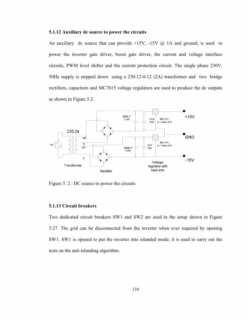
124
5.1.12 Auxiliary dc source to power the circuits
An auxiliary dc source that can provide +15V, -15V @ 1A and ground, is used to
power the inverter gate driver, boost gate driver, the current and voltage interface
circuits, PWM level shifter and the current protection circuit. The single phase 230V,
50Hz supply is stepped down using a 230:12-0-12 (2A) transformer and two bridge
rectifiers, capacitors and MC7815 voltage regulators are used to produce the dc outputs
as shown in Figure 5.2.
Figure 5. 2 : DC source to power the circuits
5.1.13 Circuit breakers
Two dedicated circuit breakers SW1 and SW2 are used in the setup shown in Figure
5.27. The grid can be disconnected from the inverter when ever required by opening
SW1. SW1 is opened to put the inverter into islanded mode; it is used to carry out the
tests on the anti-islanding algorithm.
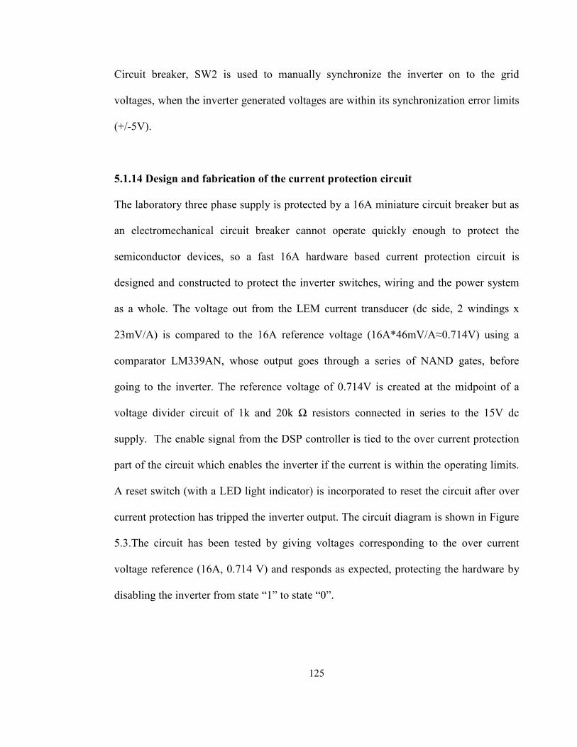
125
Circuit breaker, SW2 is used to manually synchronize the inverter on to the grid
voltages, when the inverter generated voltages are within its synchronization error limits
(+/-5V).
5.1.14 Design and fabrication of the current protection circuit
The laboratory three phase supply is protected by a 16A miniature circuit breaker but as
an electromechanical circuit breaker cannot operate quickly enough to protect the
semiconductor devices, so a fast 16A hardware based current protection circuit is
designed and constructed to protect the inverter switches, wiring and the power system
as a whole. The voltage out from the LEM current transducer (dc side, 2 windings x
23mV/A) is compared to the 16A reference voltage (16A*46mV/A≈0.714V) using a
comparator LM339AN, whose output goes through a series of NAND gates, before
going to the inverter. The reference voltage of 0.714V is created at the midpoint of a
voltage divider circuit of 1k and 20k Ω resistors connected in series to the 15V dc
supply. The enable signal from the DSP controller is tied to the over current protection
part of the circuit which enables the inverter if the current is within the operating limits.
A reset switch (with a LED light indicator) is incorporated to reset the circuit after over
current protection has tripped the inverter output. The circuit diagram is shown in Figure
5.3.The circuit has been tested by giving voltages corresponding to the over current
voltage reference (16A, 0.714 V) and responds as expected, protecting the hardware by
disabling the inverter from state “1” to state “0”.

126
15V DC
20k Ohms
1k Ohms
2.2k Ohms
1.5k Ohms
Reset Switch (Spring Return):
High Always, Low to reset
H/W Enable
DSP Enable
(Anti-islanding protection)
_____
Reset
-+
CT
CTCT
CT
0.714 V
_________
_Over
Current
LEM Current Sensor
2 windings x 23mV/Amp
16A Current protection circuit
LM339AN
HEF4011BP
100u F
Fig
ure
5. 3:
Curr
ent
pro
tect
ion c
ircu
it

127
5.1.15 Design and fabrication of the measurement interface circuitry
This section provides a description of the hardware circuits developed for the
DSP controller to communicate with the constructed inverter. Measurement signals that
are sensed for control purposes need conditioning before being fed into the DSP and
actuator signals that are given to the inverter by the DSP need to be appropriately
conditioned to be fed into the inverter and the boost gate drivers.
The measurement interface card, as the name suggests is the interface between different
current and voltage signals used for control purposes and the DSP, as represented in
Figure 5.4. Eight different current and voltage signals have to be fed in to the DSP for
control and monitoring purposes.
Figure 5. 4: Measurement interface card
The DSP used for this purpose (DS1104) can handle only -10V to +10V input signals.
Therefore an interfacing circuit is required, which can output appropriate voltage signals.
Interface cards have to be designed for handling eight measurements:
a) 400 V ac Pk - grid phase voltages (for each phase)
b) 1000V dc -for inverter dc link
c) 600V dc- for dc source voltage
d) 25A ac Pk - for injected currents (per phase)
e) 25A dc- for dc source current
Voltage and
Current
Signals
DS1104
dSpace
controller
board
Measurement Interface
Card

128
The voltage and current signals are passed through this circuitry for conditioning and
then acquired at the ADC sampling frequency (5 kHz). The attenuator stage of the
measurement interface circuits provides a high impedance barrier with built in
redundancy for safety. Figure 5.5 shows the different steps involved in conditioning the
signals.
Figure 5. 5: Measurement interface card circuitry
The purpose of each stage is explained in the following section:
1. Attenuator/transducer: The voltage signal is sensed and passed through a resistive
network where it is attenuated to a lower level. The live and neutral of each phase are
measured differentially therefore the same resistive network exists on both terminals. 1
% precision resistors are chosen to give accurate measurements and this resistive
network avoids use of bulky and costly transformers for the attenuation stage. The
current signal is passed through a current transducer (LEM, LTA 200-S) and a voltage
signal proportional to that is obtained.

129
2. Differential amplifier: The difference of the signals at inputs is amplified at this
stage. The Common Mode Rejection (CMR) property of this stage helps to reduce the
incoming noise and only the signal of the interest is amplified. The circuit design of the
differential amplifier (TL084) is shown here in Figure 5.6.
Figure 5. 6: Differential amplifier stage
The ac gain of this stage is designed to be 0.5 for the voltage channels and 1 for the
current channels.
3. Anti aliasing filter: This low pass filter helps to remove the high frequency noise,
which can cause aliasing effects upon sampling of the signal. This filter was designed to
remove any noise signals above 500 kHz (–40 dB amplitude distortion) keeping in mind
the sampling frequency of the analogue to digital converter (ADC) channels of DSP. It
was decided to build Butterworth filters because of their smooth response in pass band
frequency range. The cutoff frequency of the filter is given by equation below:

130
RCπ2
1Fc =
The value of R and C can be designed based on this equation by fixing the cutoff
frequency. The gain of the filter is given by equation below:
1
1R
RG
f+=
For voltage measurement
The ac gain of the third order filter stage is 2.96. Based on this value the resistors R1 and
Rf can be decided (see Table 5.1). A third order filter was designed to pass 2.5 kHz (50th
Harmonic of 50 Hz signal) signal with magnitude error of 0.04% and phase error of
3.96o
for the voltage measurement channels. The circuit diagram of the third order filter
is shown in Figure 5.7.
Figure 5. 7: Circuit diagram of 3rd
order Butterworth filter
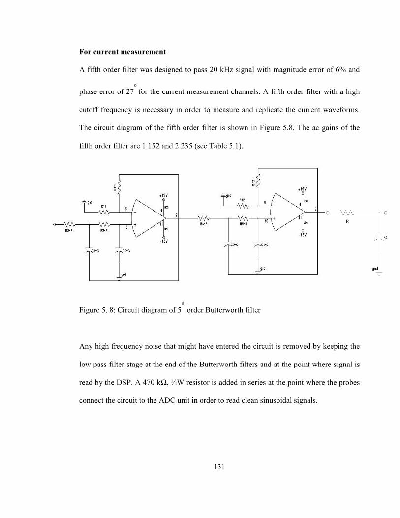
131
For current measurement
A fifth order filter was designed to pass 20 kHz signal with magnitude error of 6% and
phase error of 27o
for the current measurement channels. A fifth order filter with a high
cutoff frequency is necessary in order to measure and replicate the current waveforms.
The circuit diagram of the fifth order filter is shown in Figure 5.8. The ac gains of the
fifth order filter are 1.152 and 2.235 (see Table 5.1).
Figure 5. 8: Circuit diagram of 5th
order Butterworth filter
Any high frequency noise that might have entered the circuit is removed by keeping the
low pass filter stage at the end of the Butterworth filters and at the point where signal is
read by the DSP. A 470 kΩ, ¼W resistor is added in series at the point where the probes
connect the circuit to the ADC unit in order to read clean sinusoidal signals.

132
4. Over voltage protection
The signals pass through an over-voltage protection circuit shown in Figure 5.9 before
they are read by the ADC ports of the DSP. The ADC of DSP is very sensitive to voltage
input other than the specified level. Therefore, the protection circuit ensures to keep the
output voltage between -10 and +10 Volts. Resistors of 1% precision and zener diode
BAT85 based voltage clamping circuit is added to the end, of each of the measurement
interface circuits.
Figure 5. 9: Over-voltage protection circuit
The simulation study of the designed circuits has been carried out in the simulation
package LT Spice. The schematic diagrams of the five different measurement circuits
and their simulation results are given in Figures 5.10 to 5.20.
Each stage of the circuit was built and tested individually and then put together for a
breadboard testing. Differential mode and common mode tests were carried out on each
of the measurement channels of the circuit to ensure their reliable operation. The test
results were satisfactory and show the input signals are conditioned as expected; also ac
and dc gains of the circuits were consistent in the tests carried out. Also differential and

133
common mode frequency tests were carried out on the circuit. Finally they have been
built on the Vero Board whose hardware test results are shown in Figures 5.28 to 5.30 in
Section 5.4. The hardware circuit implementations are shown in Appendix 6.
Table 5.1 below gives the Figure number, parameters and the respective Figure numbers
showing results, for all the different measurement interface circuits.
Table 5. 1: Measurement interface circuit parameters
Figure Interface circuit Anti-aliasing filter gain
1
1R
RG
f+= , Rf,R1-Ω
Low pass
filter,
R-Ω,C-µF
Simulation
result
shown in
Figure
5.10 ac voltage Rf=100k, R1=51k, G=2.96 R=180
C=0.01
5.11 and
5.12
5.13 dc link Rf=33k, R1=51k, G=1.65 R=180
C=0.01
5.14
5.15 dc source Rf=100k, R1=51k, G=2.96 R=180
C=0.01
5.16
5.17 ac current Rf=20k,R1=130k, G=1.152
Rf=160k, R1=130k, G=2.235
R=100,
C=0.01
5.18
5.19 dc current Rf=20k, R1=130k, G=1.152
Rf=160k, R1=130k, G=2.235
R=100,
C=0.01
5.20

134
Fig
ure
5. 10:
AC
volt
age
inte
rfac
e ci
rcuit
Fig
ure
5. 11:
Sim
ula
tion r
esult
of
the
ac v
olt
age
inte
rfac
e ci
rcuit
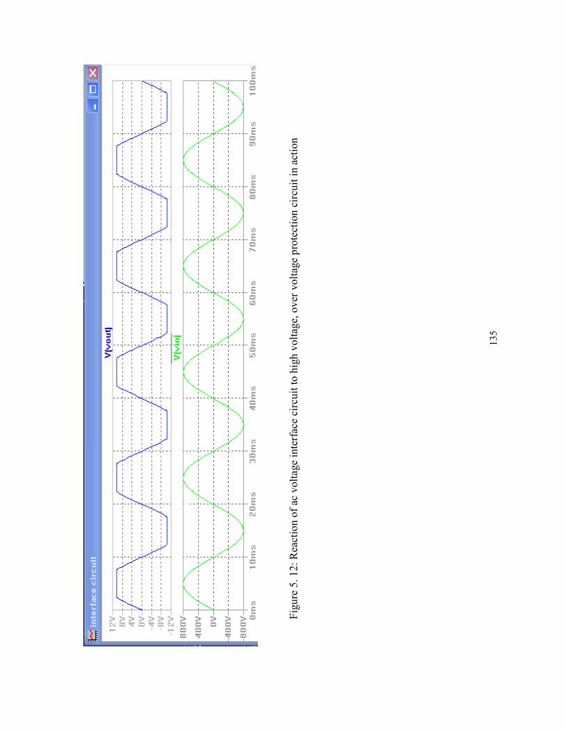
135
Fig
ure
5. 12:
Rea
ctio
n o
f ac
volt
age
inte
rfac
e ci
rcuit
to h
igh v
olt
age,
over
volt
age
pro
tect
ion c
ircu
it i
n a
ctio
n

136
Fig
ure
5. 13:
DC
lin
k i
nte
rfac
e ci
rcuit
Fig
ure
5. 14:
Sim
ula
tion r
esult
of
the
dc
link i
nte
rfac
e ci
rcuit

137
Fig
ure
5. 15:
DC
sourc
e in
terf
ace
circ
uit
Fig
ure
5. 16:
Sim
ula
tion r
esult
of
the
dc
sourc
e in
terf
ace
circ
uit
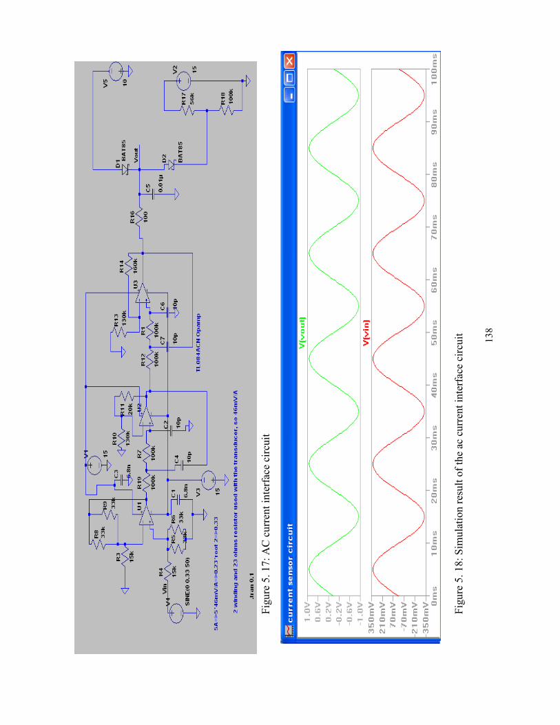
138
Fig
ure
5. 17:
AC
cu
rren
t in
terf
ace
circ
uit
Fig
ure
5. 18:
Sim
ula
tion r
esult
of
the
ac c
urr
ent
inte
rfac
e ci
rcuit

139
Fig
ure
5. 19:
DC
cu
rren
t in
terf
ace
circ
uit
Fig
ure
5. 20:
Sim
ula
tion r
esult
of
the
dc
curr
ent
inte
rfac
e ci
rcuit
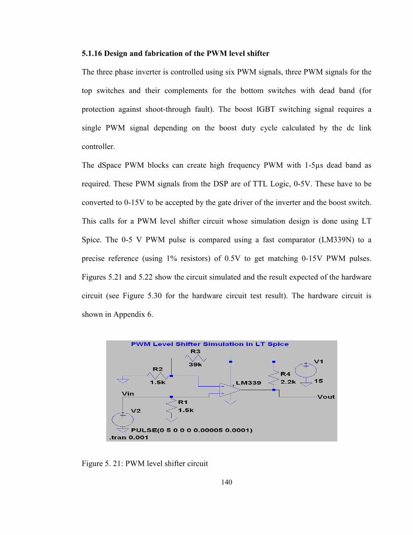
140
5.1.16 Design and fabrication of the PWM level shifter
The three phase inverter is controlled using six PWM signals, three PWM signals for the
top switches and their complements for the bottom switches with dead band (for
protection against shoot-through fault). The boost IGBT switching signal requires a
single PWM signal depending on the boost duty cycle calculated by the dc link
controller.
The dSpace PWM blocks can create high frequency PWM with 1-5µs dead band as
required. These PWM signals from the DSP are of TTL Logic, 0-5V. These have to be
converted to 0-15V to be accepted by the gate driver of the inverter and the boost switch.
This calls for a PWM level shifter circuit whose simulation design is done using LT
Spice. The 0-5 V PWM pulse is compared using a fast comparator (LM339N) to a
precise reference (using 1% resistors) of 0.5V to get matching 0-15V PWM pulses.
Figures 5.21 and 5.22 show the circuit simulated and the result expected of the hardware
circuit (see Figure 5.30 for the hardware circuit test result). The hardware circuit is
shown in Appendix 6.
Figure 5. 21: PWM level shifter circuit

141
Figure 5. 22: Simulation result of the PWM level shifter circuit
These 0-15V PWM signals taken by the inverter and the boost switch are conditioned
(using high frequency isolating transformers) within their respective gate driver circuits
that are selected for operation. Firstly they are modulated with a very high frequency
carrier and then isolated using an isolation transformer. This protects the DSP controller
board from any damage.

142
5.2 Software control (Simulink control program and dSpace DS1104 controller)
Modern power electronic systems require, sophisticated high speed control, fast
triggering protection schemes and data communication systems. The control complexity
of the three-phase dc-ac grid connected inverter requires a microprocessor or a digital
signal processor to test its various algorithms run together. A DSP based digital
controller is developed to control the hardware prototype.
A DS1104 controller board (DSP board) along with the CP1104 panel (that interacts
with the signals) has been used to run the Simulink algorithm, to control the constructed
hardware prototype.
The objective of the power electronic converters for utility interconnection is to supply
high quality power output to the utility grid. In compliance with the IEEE Std. 929-2000
[3], the IEEE Std. 1547-2003 [4] and EN50438 European standard [5], the real power
output is maintained constant to minimize current and/or voltage harmonic distortion at
the point of interconnection and the reactive power output is regulated to zero to achieve
power factor near unity.
Synchronisation to the grid is a vital function of the grid tie inverter during start up, to
avoid faults with mismatched voltage (as discussed in Chapter 2). This synchronisation
information from the grid is also used to run the inverter at unity power factor (i.e.
current produced by the inverter is in phase with the grid voltage).
The next section describes the control program and the respective flow chart is given
below in Figure 5.23. There are further discussions on how the Simulink program is
developed, downloaded on to the DSP processor and the GUI designed to interact with
the user in real-time.

143
5.2.1 Control program
The control program is written in Simulink with Sim Power System, dSPace and other
relevant block sets. Maximum step size achieved without making the processor go into
over run situation is 0.0002 s for the whole program. All ADC’s are sampled at 5000 Hz
in the control program running all blocks at the same speed, except the block that
calculates M and δ which is sampled at 50Hz. This is because the inverter output takes
time to reflect the new reference and a high sampling frequency is not required. Even
though a 5000 Hz program sample rate is sufficient for the developed control algorithm
with all the protections and anti islanding scheme running, it is noted as a drawback of
the dSpace system DS1104 that it cannot achieve a very high sampling rate with larger
Simulink programs. Full Simulink control program with its subsets is shown in
Appendix 5.
The three-phase grid voltages (75V rms L-N) are sensed at 5000 Hz (100 samples per
frequency cycle giving an uncertainty of 3.6°) and they are expected to be sinusoidal
with a peak value of 106V on the secondary side of the three-phase step down
transformer. 400V L-L, 230V L-N three-phase utility grid is connected on the primary
side. These sensed voltage signals go through a series of steps and calculations in order
to make appropriate control decision for transfer of real power to the grid from the
inverter. The main steps involved in the control program (Figure 5.23 in Section 5.2.4)
are discussed below.
The RMS and peak value )2( ×RMS of these acquired grid voltages are calculated
continuously. The sensed grid signals are divided by the fixed peak value (106V) to get a
sinusoidal normalised to 1V Pk-Pk, which is the normalised grid voltage signal. Any

144
voltage distortion, sag or swell is directly reflected on the normalised grid signal with
this process. Positive sequence component is retrieved for the above three-phase voltage
signals which go through a PLL.
The three-phase discrete PLL is then used to retrieve the frequency and phase
information ( tω ) of these normalised grid voltage signals. The RMS of the three grid
voltages, along with the Iref (inverter ac current reference), Vdc (dc link voltage) and Z
(value of coupling impedance of LCL filter), are used to calculate the Vinv Pk (required
inverter peak voltage) and δ (lead angle) continuously, using the power flow theory
discussed earlier in Section 2.4 of Chapter 2. The Vdc is sensed simultaneously. The M
(modulation index) is calculated using Vdc to produce the required Vinv.
Vinv, δ and M along with the tω information is used to generate three sinusoidal
reference signals for generation of three PWM pulses at 20 kHz that switch the three top
switches of the inverter block. Inverted sinusoidal references are used to generate three
inverted 20 kHz switching pulses that switch the three bottom switches. A 3µs dead band
(blanking time) is added to the bottom switching signals to avoid shoot through.
5.2.2 DC link voltage control
The dc link controller is based on a programmed embedded Matlab script which keeps
the dc link voltage within the band 285-305V by controlling the duty cycle of the boost
switch accordingly. If dc link voltage below 285V is sensed, the duty cycle is increased
in steps of 0.0001 and if voltage above 305V is sensed then duty cycle is decreased in
steps of 0.0001. This step size is carefully chosen in order to keep up with the 5000 Hz
sampling frequency of the control program. Minimum dc link voltage required to operate

145
safely without boosting is 265V and the minimum dc source voltage expected is 150V
when the boost stage is operating. Figure 5.37 shows the response of the dc link voltage
control algorithm that adjusts the boost converter’s duty cycle accordingly depending on
the applied dc source voltage (a big step of 210V to 286V in the dc source voltage is
made). The step response of the dc link controller shows that the dc link voltage is
quickly (within 1 second) adjusted to the reference band. The controller always stops
perturbing in the same direction after reaching a predefined maximum duty cycle (30-
50% user defined maximum value) and does not boost beyond this for safety reasons.
See A.5.8 in Appendix 5 for the algorithm.
5.2.3 Inverter protection
To protect the inverter from operating beyond nominal frequency and voltages,
embedded Matlab scripts are used to stop the inverter when one of the following occurs:
1. Passive islanding protection: Any of the phase voltages are out of +/-10% voltage
range
2. Passive islanding protection: Frequency is out of the range of 48 to 50.5 Hz
3. DC link voltage exceeds 450V
4. User Enable is ‘0’ instead of ‘1’
5. Proposed anti-islanding protection algorithm output is ‘0’ instead of ‘1’ ( This
new technique is described in the Chapter 6 of this thesis)
6. DC side current exceeds 16A
Frequency protection algorithm is shown below, rest of the protection algorithms
developed (which are similar in nature) are shown in A.5.8 of Appendix 5.

146
function [y,T] = Freq_protection(u,T1)
% This block supports the Embedded MATLAB subset.
% See the help menu for details.
y=1; T=50;
if (u>50.5 || u<48)% once threshold reached, upper limit (+1%), lower limit (-4%),switch
is put to zero, 48 to 50.5 for 50Hz
y=0;
T=u;
end
if (T1>50.5 || T1<48)
y=0;
T=T1;
end
T1=T; %T1=T=0 until U>th, then T1=T=U and it keeps the switch to zero(i.e inverter is
disabled continuously)

147
5.2.4 Control flow chart
Figure 5. 23: Control program flow chart

148
5.2.5 Software development
The software that runs on the DS1104 controller board are the simulink files that are
created for simulation purposes, but unlike in simulation; many blocks have been
replaced and modified with blocks from the ‘dSPace tool box’ to communicate with the
real signals from the hardware.
Two simple examples of the many changes made to the Simulink simulations are:
1. The simulated program contained a “three-phase grid block’’ from Sim Power
Systems blocksets in Simulink. This now is replaced by connecting the real
utility grid. PCC voltages acquired using the ADC port passes through a gain of
10 before appropriate gain (real signal which was conditioned and attenuated by
the interface circuit needs to be amplified within the control program) is utilised.
2. Carrier based sinusoidal PWM was generated by comparing high frequency
carrier against a sinusoidal reference to generate PWM for each switch, during
simulations. This is now replaced by generating duty cycle references 0-1 V, i.e a
continuous product of shifted sinusoidal reference (0-1 V) with the modulation
index, M, is fed into the “dSpace PWM block” that controls the inverter. The
sampling frequency for simulation purposes was 125 kHz while for the final
control program is only 5 kHz.
Various changes, calculation and gains required by specific blocks, have been made
precisely in order to make the final program compatible with the dSPace controller. The
solver settings have been made such that Real Time Workshop can be used to transform
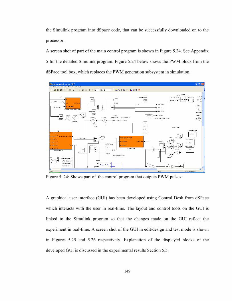
149
the Simulink program into dSpace code, that can be successfully downloaded on to the
processor.
A screen shot of part of the main control program is shown in Figure 5.24. See Appendix
5 for the detailed Simulink program. Figure 5.24 below shows the PWM block from the
dSPace tool box, which replaces the PWM generation subsystem in simulation.
Figure 5. 24: Shows part of the control program that outputs PWM pulses
A graphical user interface (GUI) has been developed using Control Desk from dSPace
which interacts with the user in real-time. The layout and control tools on the GUI is
linked to the Simulink program so that the changes made on the GUI reflect the
experiment in real-time. A screen shot of the GUI in edit/design and test mode is shown
in Figures 5.25 and 5.26 respectively. Explanation of the displayed blocks of the
developed GUI is discussed in the experimental results Section 5.5.

150
Figure 5. 25: GUI in Control Desk (design mode)
Figure 5. 26: GUI in Control Desk (Test Mode)

151
5.3 Construction and testing
The prototype construction and testing has been performed stage by stage in the
following sequence, in order to prepare the system to be able to run the experiments:
• Building of the interface circuits and testing
• Building of the main components of the inverter system, cabinet and testing
• Software development, testing and interaction with hardware
• Procurement of the cabinet, components, materials and tools
• Wiring and marking
A schematic diagram of the full experimental setup with all the measurement sensors,
circuits and DSP is shown in Figure 5.27. Pictures of the prototype at different
assembling stages are presented in Appendix 6. This work on the prototype construction,
involved practical experience and required manufacturing and engineering skills such as
mounting, assembling, wiring, programming and testing.
Testing of the prototype was done in a systematic manner. Each section and component
was tested individually before putting them together. Debugging of certain problems was
time consuming but was adopted in a modular fashion to achieve goals.
Various tests were carried out to verify safe operation of each part of the laboratory
prototype before any experiment could take place as listed below:
• Voltage and current measurement interface circuits are tested to match with
simulation results. Gains presented by hardware matched the simulation.
• LEM transducers are tested to confirm their operation and ratio of output.

152
• Inductors have been tested at four different frequencies, 100Hz, 120Hz, 1k Hz,
10k Hz using Stanford Research Systems Model SR715, LCR Meter.
• ADC input range and internal attenuation (+/-10V=>+/-1V) and DAC output
range has been tested.
• Voltage and current measurement are calibrated and internal gains within the
control software are adjusted according to two different multimeters and
oscilloscopes
• Basic PWM output is tested by using software generated grid voltages and then
sensing real grid voltages both before and after the PWM level shifter.
• The reliability of generated dead bands is confirmed if they give the appropriate
and exact width for the selected dead band before and after the PWM level
shifter.
• Current protection circuit is tested by applying equal and greater voltages to the
over current reference voltage.
• Boost circuit is tested by applying dummy duty cycle values before it is
connected as part of the grid connected inverter system.
• DC link controller is tested to see the change in duty cycle and the maximum
duty cycle reached (protection of dc link) with lower dc source voltages
(295<V>305).
• Protection algorithms written are tested with software generated over/under
frequency and voltages into the main control algorithm.
• Inverter output voltages are tested if they generate the calculated voltages.

153
• Harmonic content/ Fourier transform of both grid and inverter voltages is
analysed using the PQ monitor
• Synchronization error between grid and inverter voltage before connection is
analysed if it is within the +/-5V range.
Summary of safety measures for the experimental setup
Safety of components, hardware prototype as a whole, laboratory and human health was
given close consideration. Some important measures taken to protect them all are briefed
as follows:
• Resistor network at the attenuation stage with built in redundancy within the
interface circuits
• 12.7 Ω high power resistor in series between the dc link capacitor and inverter
input
• Three-phase step down and isolation transformer
• Choice of L and C values with ample margin than the calculated values
• Choice of operating dc link voltage
• Ultra fast 5A fuse between the variable ac source and the rectifier
• User defined maximum boost duty cycle (30-50%) for the dc link controller
• Fast 16A hardware based current protection circuit
• Software protection that disables the inverter based on 6 different signals (see
Section 5.2.3)
• Wooden cabinet

154
AC
AC
AC
Rectified
DC Source
Inverter
LCL Filter
SW2
3-Phase
AC Grid 400V
LL
Dc-Dc Boost
3-
Phase
Load
PCC
Idc
Idc
Idc
Idc
Vdc Source
Vdc Source
Vdc Source
Vdc Source
B BBB
Vdc Link
Vdc Link
Vdc Link
Vdc Link
2200
2200
2200
2200uF uFuFuF
500
500
500
500V VVV
Wavelet Analysis &
Detection of
Islanding situation
Va Vb
Vc
n
Gate Signals
WBA Enable
Enable (0-10V)
SW1 n
3-Phase
Transformer
400-130 VLL
3 x AC
Voltage
Interface
Circuit
7.5mH
7.5m
H
10uF
250V
AC
5mH
Boost (0-15V)
Enable (0-10V)
Vdc Source
Vdc Source
Vdc Source
Vdc Source
2500
2500
2500
2500uF uFuFuF
350
350
350
350V VVV
Vac Source
Vac Source
Vac Source
Vac Source ( (((Triac
Triac
Triac
Triac) )))
230
230
230
230V VVV, ,,,50 505050Hz
HzHz
Hz
dSpace
DS1104
Runs @
300V
Runs @
150-300V
CT
CTCT
CT
CT
CTCT
CT
CT
CTCT
CT
3 x AC
Current
Interface
Circuit
Synshronisation
PWM control
Vdc Link Control
Power transfer
2 x DC Voltage
&
1 DC Current
Interface Circuit
CT
CT
CT
CT
16A
current
protection
X 6
0-5V
PWM Level
Shifter
0-15V
Vdc Link
Vdc Link
Vdc Link
Vdc Link
IaIbIc F
igu
re 5
. 27 :
Ex
per
imen
tal
setu
p

155
5.4 Experimental results of the interface circuits
The hardware system and the interface circuits have been built and tested in the
laboratory. Measurements have been performed using LEM LTA 50P/SP1 & LTA
100P/SP1 current transducers, Tektronix oscilloscope type TPS 2024, Tektronix
oscilloscope type THS720P, Farnell 2 x 15V dc source E30-2BT, variable rectified dc
source that was built in the laboratory for the setup, single phase 230V 50Hz grid supply
and three-phase step down transformer 400:130V L-L has been used in the experiment.
Figure 5.28 shows the hardware result obtained from the ac voltage interface circuit and
Table 5.2 gives the attenuation factors from the test performed on the ac voltage
interface circuit. Figure 5.29 shows the hardware result obtained from the dc source
voltage interface circuit and Table 5.3 gives the attenuation factors from the test
performed on the dc source voltage interface circuit. Table 5.4 and Table 5.5 show the
attenuation and gain factors of the tests performed on the dc link voltage interface circuit
and current interface circuit respectively. Figure 5.30 shows the hardware result obtained
from the PWM level shifter circuit. Experimental test results below show interface
circuits built on the veroboard are complying with the simulation results and the gains of
the circuits have been consistent throughout the tests.
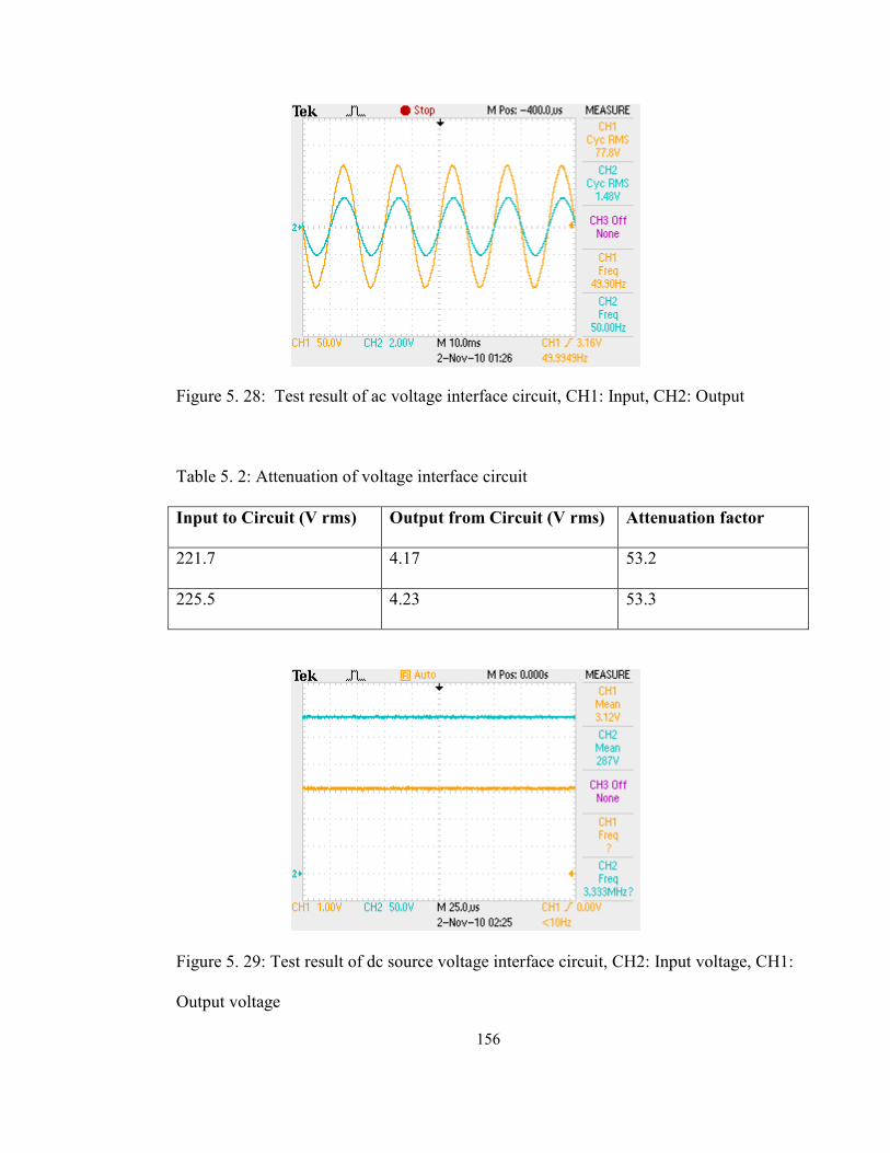
156
Figure 5. 28: Test result of ac voltage interface circuit, CH1: Input, CH2: Output
Table 5. 2: Attenuation of voltage interface circuit
Input to Circuit (V rms) Output from Circuit (V rms) Attenuation factor
221.7 4.17 53.2
225.5 4.23 53.3
Figure 5. 29: Test result of dc source voltage interface circuit, CH2: Input voltage, CH1:
Output voltage

157
Table 5. 3: Attenuation of dc source interface circuit
Input to Circuit (V rms) Output from Circuit (V rms) Attenuation factor
287 3.12 92
300 3.27 91.7
Table 5. 4: Attenuation of dc link interface circuit
Input to Circuit (V rms) Output from Circuit (mV
rms)
Attenuation factor
50.6 365 138.6
50.8 366 139
100 730 137
100.2 732 136.8
127.4 934 136.4
Table 5. 5: Gain of current interface circuit
Input to Circuit (V rms) Output from Circuit (V rms) Gain factor
3 8.59 2.86
1 2.85 2.85

158
Figure 5. 30 : Test result of PWM Level shifter circuit, CH1: Input 0-5V PWM, CH2:
Output 0-15V PWM
5.5 Experimental results of the system
The grid voltages Va, Vb, Vc, Vdc source, Vdc link voltage, grid frequency and the
current flowing through phase A are acquired and displayed (see Figure 5.34). Figure
5.31 shows a close view of the sensed grid voltages during a period of 0.02s. Figure 5.31
shows: (a) the voltage signal sensed by ADC, (b) gain of 10 applied on the ADC signal
(dSpace has an internal attenuation of 10), (c) normalized grid voltage signal that is fed
into the PLL and (d) sensed ADC signal scaled to achieve full grid voltage signal that is
used for calculations. Figure 5.34 and 5.35 show the screen shots of dSpace Control
Desk GUI in acquisition mode, while the inverter is up and running.

159
Figure 5. 31: Close view of the sensed ADC voltages
(a) ADC signal, (b) ADC with gain of10 (c) Normalized grid voltage (d) Grid voltage-
appropriate gains applied to retrieve real signal
Calculated values for each phase that include RMS voltages at PCC, required inverter
peak voltage, modulation index and lead angle to transfer 0 Amps (synchronization
mode) are displayed at startup. The user has the option to start the inverter by clicking on
‘DSP Enable’. This allows the inverter to generate matching voltages to the PCC. The
synchronization error can be checked on the oscilloscope to be in the limits +/-5V RMS
before connecting to the grid as shown in Figure 5.32. Once the synchronization error is
within the limits, the synchronization manual circuit breaker SW 2 is closed and the
inverter is ready to transfer power as shown in Figure 5.33.
(a) (c)
(d)
(b)
Time(s) Time(s)
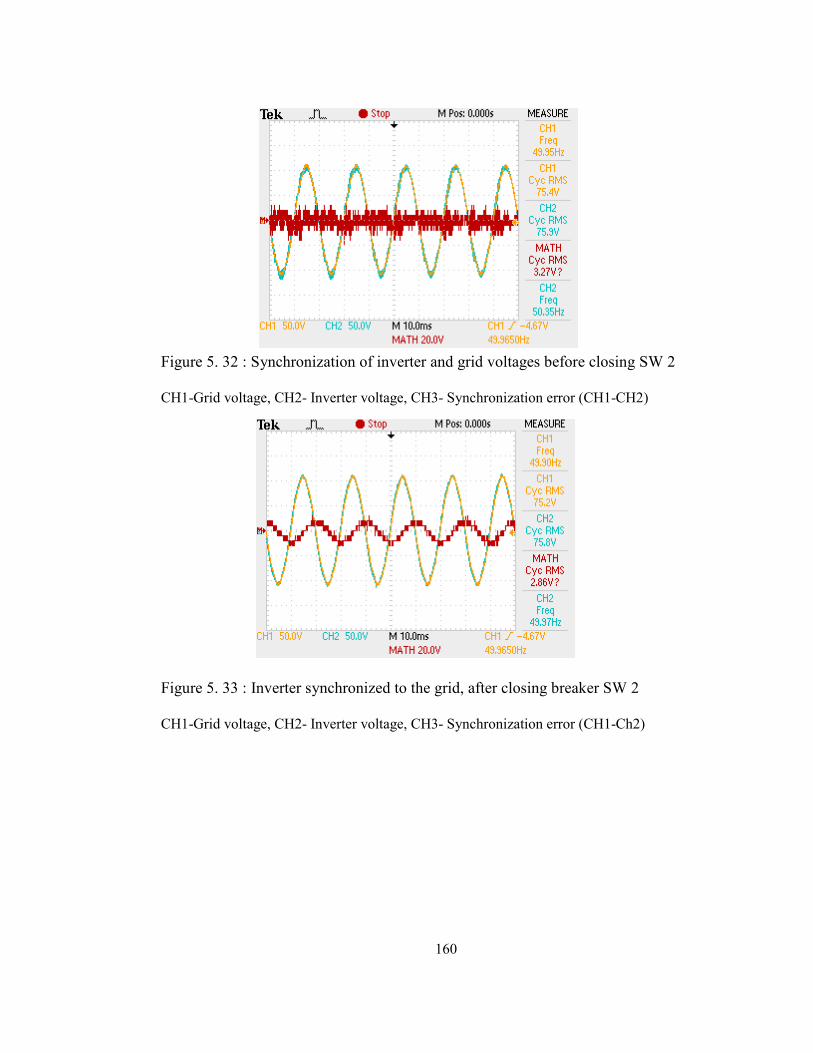
160
Figure 5. 32 : Synchronization of inverter and grid voltages before closing SW 2
CH1-Grid voltage, CH2- Inverter voltage, CH3- Synchronization error (CH1-CH2)
Figure 5. 33 : Inverter synchronized to the grid, after closing breaker SW 2
CH1-Grid voltage, CH2- Inverter voltage, CH3- Synchronization error (CH1-Ch2)

161
Depending on the level of reference current, corresponding current is transferred into the
grid as shown in Figure 5.34. The calculations are made continuously in real time for the
new reference current and updated on the GUI. In this case 1.85A current is flowing in
each phase of the power circuit from the inverter to the grid.
If the boost circuit is switched ‘On’ within the GUI, then the dc link voltage is boosted to
voltages between 285V and 305V. Also, the required duty cycle fed to maintain the dc
link voltage is displayed as shown in Figure 5.35. Figure 5.36 shows the close view of
the sensed, real dc source voltage and the real boosted dc link voltage when boost circuit
is operating.
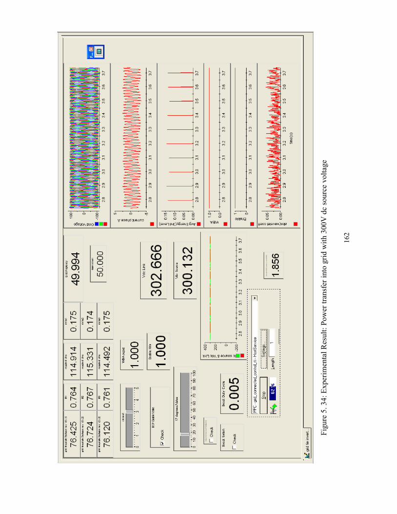
162
Fig
ure
5. 34:
Ex
per
imen
tal
Res
ult
: P
ow
er t
ransf
er i
nto
gri
d w
ith 3
00V
dc
sourc
e volt
age
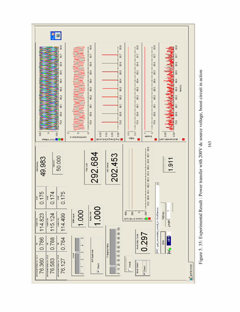
163
Fig
ure
5. 35:
Ex
per
imen
tal
Res
ult
: P
ow
er t
ransf
er w
ith 2
00V
dc
sourc
e volt
age,
boost
cir
cuit
in a
ctio
n
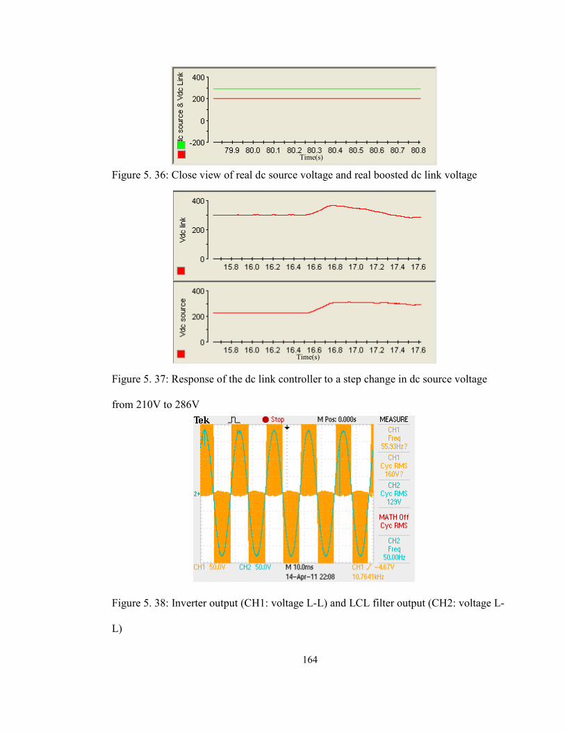
164
Figure 5. 36: Close view of real dc source voltage and real boosted dc link voltage
Figure 5. 37: Response of the dc link controller to a step change in dc source voltage
from 210V to 286V
Figure 5. 38: Inverter output (CH1: voltage L-L) and LCL filter output (CH2: voltage L-
L)
Time(s)
Time(s)

165
5.6 Conclusion
The Chapter detailed the selection of components, calculations and designs
necessary for the grid connected inverter prototype. The details of the interface circuit
design and their circuit configuration used between the hardware and DSP are provided.
Simulation results and hardware test results of the respective circuits are produced and
compared. The developed software control algorithm is described in detail with a flow
chart and the development of the program for the chosen DSP has been explained. Full
experimental results of the working system are produced with the designed GUI in
dSpace Control Desk. The phase locked loop performed better than expected in tracking
the zero crossings and transferring a steady current into the grid (i.e. having a 3.6°
sampling uncertainty should allow at least 1A fluctuation at inverter current output). The
experimental results show the successful completion of the three phase grid connected
inverter hardware construction, software control program and their smooth interaction.
Results are as expected and proven to be satisfactory according to the EU EN50438
standard. The experimental setup is ready to perform more tests on the proposed anti
islanding scheme which is discussed next in Chapter 6.

166
Chapter 6
6. NOVEL ANTI-ISLANDING TECHNIQUE PROPOSED USING
WAVELET ANALYSIS
6.0 Introduction
Islanding of grid-connected PV inverters occurs when the local network containing such
inverters is disconnected from the main utility, but the PV inverters continue energizing
the local load without control and/or supervision of utility. This phenomenon can result
in a number of potential hazards [58], [59].
• Maintenance staff may be harmed when arriving to service the energized isolated
network.
• Utility customer’s equipment/devices may be damaged due to uncontrolled
voltage and frequency excursion outside nominal range.
• Switching and measuring devices may be damaged due to unsynchronized out of
phase re-closure.
• Islanding may interfere with automatic reclosing devices of the utility (devices
may malfunction).
Basic passive protection schemes include over-current, over- and under-voltage, and
over- and under-frequency (OV/UV and OF/UF) functions to remove a grid connected
inverter from the utility grid for the abnormal condition in the grid. Also, anti-islanding
schemes must be incorporated into protection control. The above OV/UV/OF/UF
schemes are able to detect islanding operation of the grid connected inverter. In case of
PV (DG), however, inverter generation being balanced with local load, it is impossible to

167
detect islanding using basic schemes (non-detection zone, NDZ), and hence at least one
active anti-islanding scheme must be included in protection (to eliminate NDZ) [44].
This active islanding scheme injects certain signals (perturbation to variables like voltage
and frequency) in order to detect the islanding situation which degrades the output power
quality [46], [55], [56].
In response to the above mentioned problem, a detailed literature survey is conducted on
the present islanding detection schemes. Then a new anti-islanding technique which uses
wavelet modulation is proposed. The Wavelet Modulation technique is used to look at
the physical measurements (voltage, frequency, voltage unbalance) in a higher
dimension, to see the changes in parameters in a passive environment rather than
injecting any perturbation.
6.1 Review of islanding detection
A detailed review revealed several islanding detection methods [44]-[60], which can be
classified as passive, active and other methods. Their significant strengths and weakness
are discussed below.
6.1.1 Passive methods
6.1.1.1 Under/over voltage and under/over frequency detection
In over/under voltage and over/under frequency detection (OVP/UVP and OFP/UFP),
the voltage at the point of common coupling (PCC) and the frequency of the inverter at
PCC (node a in Figure 6.1) are continuously monitored [49], [59]. The inverter should be
disconnected to prevent damage to both the inverter and utility, when the voltage or the

168
frequency are out of specified thresholds (207V ≤ V ≤ 253V ) and (48 Hz ≤ f ≤50.5 Hz)
specified by the EN 50438 [5].
Figure 6. 1: Power flow diagram (real and reactive power mismatch)
Figure 6.1 shows a power flow diagram, where real and reactive power mismatch at the
instant utility is disconnected can be analysed. Real and reactive power mismatch is the
difference between real and reactive power consumed by the load and real and reactive
power supplied by the PV inverter, just before utility is disconnected. This can be
expressed as (6.1) and (6.2):
PVLoad PPP −=∆ (6.1)
PVLoad QQQ −=∆ (6.2)
If the PV inverter was transferring power at unity power factor, then
0=PVQ And LoadQQ =∆
It is usually assumed that the load can be modeled as a parallel RLC circuit as shown in
Figure 6.1. For most islanding detection methods, it is some type of RLC load that causes
the most difficulty in detection. General nonlinear loads such as harmonic-producing
loads or constant-power loads do not exhibit as much difficulty in islanding prevention.

169
RLC loads with a high q (Quality factor) are most problematic for islanding detection.
The quality factor can be expressed as (6.3):
L
CRq = (6.3)
The parameters R, L and C give the relative amounts of energy storage and energy
dissipation.
Real and reactive power of the load can be expressed as (6.4) and (6.5):
R
VP PV
Load
2
= (6.4)
)1
(2
CL
VQ PVLoad ωω
−= (6.5)
Real and reactive power supplied by the PV inverter can be expressed as (6.6) and (6.7):
θCosIVP PVPVPV = (6.6)
θSinIVQ PVPVPV = (6.7)
Where PVPV IV , are RMS values and θCos is the displacement factor
At the instant when island is formed (utility disconnected), the system behavior depends
on P∆ and Q∆ as follows:
(∆P>0): The inverter terminal voltage will increase above the nominal system
voltage.
(∆P<0): The inverter terminal voltage will decrease below the nominal system
voltage.
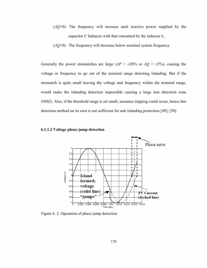
170
(∆Q>0): The frequency will increase until reactive power supplied by the
capacitor C balances with that consumed by the inductor L.
(∆Q<0): The frequency will decrease below nominal system frequency.
Generally the power mismatches are large (∆P > ±20% or ∆Q > ±5%), causing the
voltage or frequency to go out of the nominal range detecting islanding. But if the
mismatch is quite small leaving the voltage and frequency within the nominal range,
would make the islanding detection impossible causing a large non detection zone
(NDZ). Also, if the threshold range is set small, nuisance tripping could occur, hence this
detection method on its own is not sufficient for anti islanding protection [49], [50].
6.1.1.2 Voltage phase jump detection
Figure 6. 2: Operation of phase jump detection

171
This technique monitors the phase difference between the system utility voltage and
inverter output current [44], [46]. The output current is usually synchronized with the
utility voltage at unity power factor (using a PLL). Soon after the utility is disconnected,
if there is a sufficiently large power mismatch, inverter voltage is shifted to match the
difference in power and to maintain the phase angle of the load. This causes a voltage
phase jump as shown in Figure 6.2. This phase jump can be detected if it goes out of the
nominal range, again setting the threshold too small would case nuisance tripping [59].
6.1.1.3 Voltage harmonic detection
Total harmonic distortion of the system voltage at node a in Figure 6.1 is continuously
monitored [47]. With the presence of utility, the system voltage is stiff and sinusoidal
(THD close to zero), this make the inverter produce a sinusoidal current. The current
harmonics produced by a grid connected converter should be less than 5% according to
EN 50438 [5]. The current harmonics being small, interact with the small grid
impedance producing small distortion in voltage at node a (Figure 6.1). When the utility
is disconnected, a large impedance of the load interacts with the small current THD,
produces large distortion in voltage making it go out of the threshold range and hence
detecting islanding situation. THD threshold should be set appropriately in order to
operate without nuisance tripping. This method fails when the islanded load is having a
high q factor, which acts as a low pass filter in reducing the harmonic content of the
output current. Resistive load usually makes the detection easier since 5% of THD in
current causes 5% of THD in voltage and the THD limit should be less set than 5%. This

172
method also fails if the PV inverter delivers very high quality current, which produces
high quality voltage even during the presence of resistive load [46], [47].
6.1.2 Active methods
6.1.2.1 Output power variation and impedance measurement
These two active methods are put together in this survey as they work on the same
principle of changing the output power periodically and observing the changes on the
voltage at PCC (node a in Figure 6.1).
Output current can be expressed as )( PVPVPVPV tSinIi φω += (6.8)
The parameters frequency ( PVω ), phase ( PVφ ) and amplitude ( PVI ) can be perturbed in
the expressed current equation. Usually the current amplitude is perturbed and the
voltage change respective to current is observed (PV
PV
di
dv), for this reason it is also called
the impedance measurement detection [59], [60].
Impedance measurement: If impedance is observed specifically rather than the output
voltage, then a threshold for impedance needs to be set to a small value since the grid
impedance is not exactly zero. Any impedance observed below the set value indicates
grid is still connected unless the impedance of the load is below the set point which is
very rare unless the load is a high power load (approaching a short circuit).
Output power variation: Change in current amplitude ( PVI ) causes a change in output
power. Change in current or power causes a change in voltage at PCC, which when
islanded shows a significant change and gets out of the nominal threshold range. This
behavior can be used to detect the islanded situation.

173
The minimum current shift required for islanding detection is equal to the full UVP/
OVP (Under Voltage Protection/ Over Voltage Protection) window size. For instance,
with grid connected UVP/OVP at +/-10% of rated voltage, a 20% change in current is
required.
This method works quite well with a single grid connected inverter reducing the NDZ
close to zero, but fails with multiple inverters connected. When multiple inverters are
connected, change in current from one inverter is not significant and effectiveness of this
method decreases, unless the variation from all the inverters is some how synchronized
(which degrades the power quality greatly) [58], [59].
6.1.2.2 Sliding mode frequency shift (SMS)
The three parameters of the voltage at node a in Figure 6.1, to which positive feedback
can be applied are amplitude, frequency, and phase. SMS applies positive feedback to
the phase of the voltage at PCC (to the reference waveform in practical implementation)
as a method to shift the phase. The phase angle between the inverter output current and
the PCC voltage is controlled to be zero (or as close to it as possible) usually in a PV
inverter (unity power factor operation). But with SMS applied, the current-voltage phase
angle of the inverter is made to be a function of the frequency of the PCC voltage,
instead of being controlled to zero [59], [60].
The utility provides the operating point at the line frequency by providing a stable phase
and frequency reference. If an island is formed, the intersection of the load line and
inverter phase response curve gives the new operating point. The load line of the unity
power factor load (resistive load) is shown in Figure 6.3. The intersection at the point

174
labeled B, is at a frequency of 50 Hz (zero phase). This is the operating point while the
utility is connected. If the utility was disconnected and any small perturbation away
from 50Hz of the frequency of voltage at PCC, would cause the phase error to increase
(not decrease), due to the S- shaped phase response curve of the inverter. This is due to
the positive feedback mechanism, which causes a classical instability. This instability
drives the system to a new operating point, either at point A or C depending on the
direction of the perturbation. If the inverter phase curve has been properly designed for
the RLC load in Figure 6.3, points A and C would be at frequencies outside the
OFP/UFP trip window, and the inverter would shut down due to frequency error.
Figure 6. 3: Plot of the current-voltage phase angle vs. frequency characteristic of an
inverter utilizing the SMS islanding prevention method
This method is shown to be highly effective to detect islanding situations and is capable
of reducing the non-detection zone (NDZ) near to zero. It provides good compromise
between effectiveness and output power quality. This method also works well in the
multiple inverter case; however, it does fail to detect an island if the starting phase angle
matches with the load phase angle at frequency located within the threshold. It also fails,

175
if the rate of change of the starting phase angle with respect to the frequency is less than
that of the load line [60].
6.1.2.3 Active frequency drift (AFD)
Active frequency drift method is to force the frequency of PV inverter output, up or
down using positive feedback to accelerate the frequency of the inverter current [52]-
[54]. An island is confirmed, if the frequency is out of the OFP/UFP trip window (48 Hz
≤ f ≤ 50.5 Hz).
In Figure 6.4: VutilT is the period of the utility voltage, IpvT is the period of the sinusoidal
portion of the ‘PV inverter current output’, and zt is a dead or zero time.
The chopping fraction (cf) is expressed as (6.9):
VutilT
z2tcf = (6.9)
The PV inverter current output is a sinusoid with a frequency slightly higher than that of
the utility voltage during the first half cycle. The inverter output current remains at zero
for time zt before beginning the second half cycle as shown on Figure 6.4. The PV
inverter output current is a negative sinusoid with a frequency slightly higher than that of
the utility voltage during the second half cycle and again reaches zero. It remains at zero
until the rising zero crossing of the utility voltage. The zero time in the second half cycle
is not fixed and need not be zt .

176
Figure 6. 4: Output current waveform (upward active frequency drift) compared to pure
sine wave
During an islanding situation, if this current is applied to a resistive load, the voltage
would go to zero for a shorter time (TVutil - tz), as voltage follows the distorted current.
This causes the rising zero crossing of the voltage at PCC to occur sooner than normal
operation, giving rise to a phase error between PCC voltage and inverter current output.
The PV inverter then increases the frequency of current in order to eliminate the phase
error. This makes the voltage of the resistive load again have its zero crossing advanced
in time with respect to where it was earlier, and the PV inverter still detects a phase error
and increases its frequency further. This cycle continues until the frequency has deviated
far enough to be detected by the OFP/UFP trip window [59].
This method slightly degrades the output power quality and also fails with multiple
inverter case unless all the inverters agree to drift their frequencies in the same direction.
This method reduces the non-detection zone compared to the passive methods but it is
not as good as the other active methods.

177
6.1.2.4 Sandia frequency shift (SFS)
Sandia Frequency Shift (SFS) is an extension of the AFD method, and it uses positive
feedback to prevent islanding.
In this method, it is the frequency of voltage at PCC to which the positive feedback is
applied.
Using positive feedback, the ‘chopping fraction’ is made to be a function of the error in
the line frequency. While the utility is connected, the stable phase frequency reference
prevents any instability in the frequency. During an island, the chopping fraction
increases with slight increase in the frequency of the voltage at PCC, it continues until
the OFP/UFP trip window detects the frequency is out of range.
Publications [59] and [60] state that this is one of the best active methods so far, but
reduces the power quality slightly during the grid connected mode as positive feedback
amplifies the changes on the grid.
6.1.2.5 Mains Monitoring Units with Allocated All-Pole Switching Devices
Connected in Series (MSD)
Mains monitoring units are automatic isolating facilities consisting of two independent,
diverse parallel mains monitoring devices with allocated switching devices connected in
series which are independently controlled. A few islanding methods are used together in
order to detect the islanding scenario [53], [60]. Impedance detection, over/under voltage
and frequency trips are commonly used in such units. Islanding is confirmed, if grid
impedance is higher than 1.25 ohm (Z > 1.25Ω) or if there is a sudden change (within a
short period) in grid impedance larger than 0.5 ohm (∆Z ≥ 0.5 Ω).

178
This method has similar pros and cons compared to the output power variation and
impedance measurement method, but additional hardware switches involved increase the
cost of the system.
6.1.2.6 Other methods
Other methods include: Reactance insertion, Power line carrier communication and
Supervisory control and data acquisition methods. These methods are implemented at
utility level and since they are beyond the scope of this project they are not discussed.
6.2 Analysis of mismatched power during islanding
-The islanding frequency iω is a function of the inverter real power PVP , reactive power
PVQ and resonant frequency of the load (LC
1) according to [49].
+=
PV
PV
iqP
Q
LC 21
1ω (6.10)
The inverter terminal voltage iV at the instant utility is disconnected, is a function of the
ratio of real power of the PV inverter and the load as expressed in (6.11)
n
LOAD
PV
i VP
PV = (6.11)
where nV = nominal system voltage
The worst case islanding condition occurs when the real power of the PV inverter is
equal to the real power of the load, i.e., LOADPV PP = , and the corresponding reactive
power is also equal, i.e., LOADPV QQ = . For this condition, the voltage and the frequency

179
at the inverter terminal continues to be the same as when the utility was connected.
Under this condition, the PV inverter fails to notice the disconnection of utility and
continues to operate, hence causing islanding. When the above described conditions are
nearly met, the variations in the voltage and the frequency may be small and may escape
the detection. This zone is called a non-detect zone (NDZ) and is shown in Figure 6.5.
Some islanding scenarios are examined as follows [48]-[51], [61].
When P∆ is large: Inverter terminal voltage will vary widely and since voltage should
be outside the nominal operating voltage range for detection, islanding condition can be
detected effectively only if ∆P > ±20%.
When P∆ is small and Q∆ is large: Islanding frequency will vary and the frequency has
to go out of nominal limit to be detected. For islanding protection, the inverter will fail to
disconnect when the load has q ≥ 2.5, ∆P = 0, and ∆Q < ±5%.
When P∆ and Q∆ are small: if ∆P (< ±20%) and ∆Q (< ±5%) then this results in
insufficient change in inverter terminal voltage and frequency respectively, which
islands the inverter within the non-detection zone (NDZ).
Figure 6. 5: NDZ for UVP/OVP and OFP/UFP

180
6.3 Proposed anti-islanding technique using wavelet analysis
Active islanding schemes usually inject certain signals (perturbation to variables like
voltage and frequency) in order to detect an islanding event. This injection degrades the
output power quality [59]-[61]. EN50438 [5] provides requirements relevant to the
performance, operation, safety, testing and maintenance of interconnections. A summary
of the essential interconnection specifications and requirements is given in Table 1 on
page 7 of [24]. According to Table 1 on page 7 [24], any active islanding technique that
involves injections is not allowed. In response to the above mentioned detection
problems and the requirements specified by EN50438, a new technique is proposed to
build an anti-islanding scheme.
The main emphasis of the proposed scheme is to reduce the NDZ to close to zero and
to keep the output power quality unchanged. The new method for islanding detection is
based on voltage measurements that are sensed at the PCC and their analysis using
discrete wavelet transform. The new method helps to reduce the NDZ without any
perturbation that deteriorates the output power quality.

181
6.3.1 Wavelet transform
Wavelets are functions, used to efficiently describe a signal by decomposing it into its
constituents at different frequency bands (or scales) [62]. Wavelet techniques have been
used in several power system applications e.g. detection, feature extraction, de-noising
and data compression of power quality waveforms, power system protection etc. [63]-
[65], [67]. Wavelet theory is well documented in several research publications related to
power engineering applications but an explanation of the wavelet theory relevant to
islanding application is provided in this section.
Discrete wavelet transform (DWT) based on Mallats’ pyramid algorithm [66], also
known as dyadic wavelet transform is the most frequently used method owing to its
simplicity and non-redundancy. A dyadic DWT of discrete time sequence ( )nx of length
N is essentially a decomposition of the spectrum of ( )x n ; ( )X ω into orthogonal sub-
bands defined by,
1
, 1, 2.....1 1
22 mmm J
TTω+ =≤ ≤ (6.12)
where, T is the sampling period associated with ( )nx and J represents the total number
of decomposition levels. DWT is implemented by specially designed bank of high pass
and low pass discrete filter units, h and g . The filters are half band filters with a cutoff
frequency of Fs / 4, a quarter of the input sampling frequency. As the input sequence
( )nx propagates through the low pass and high pass filters, the filter bank, at each stage,
decomposes the signal into low-pass and high-pass components through convolution
(and subsequent decimation) with filters g and h, respectively. The DWT representation
is composed of scaling coefficients, ( ),Jc n representing coarse or low-pass signal

182
information at level ,m J= and wavelet coefficients (also called detail coefficients),
( ),md n which represents signal detail at levels 1,....., ,m J= as shown in Figure 6.6.
Formally,
1
1
( ) (2 ) ( )
( ) (2 ) ( ).
m m
n
m m
n
c n g n k c k
d n h n k c k
−
−
= −
= −
∑
∑ (6.13)
At level m, both ( )mc n and ( )md n are composed of 2m
N− coefficients, forming a tree-like
relationship between the coefficients at successive scales. The resulting signal
decomposition 1 2[ , ,....., , ]J Jd d d c is the dyadic DWT representation of signal ( )nx .
Figure 6. 6: (a) Analysis wavelet filter banks (b) 3-stage DWT decomposition

183
6.3.2 Proposed algorithm
To resolve the problem of non-detection zone associated with passive islanding detection
methods, wavelet analysis is proposed and included with passive techniques in this
Chapter. The key idea is to utilize the spectral changes in the higher frequency
components of the PCC voltage during islanding. When islanding takes place under
NDZ conditions, conventional passive methods which are based on threshold violations
of certain PCC voltage and frequency parameters, fail to recognize it as these parameters
are well within the threshold limit. Wavelet techniques examine the spectral changes
occurring at higher frequency components of the PCC voltage due to islanding, thus
enabling the islanding detection in the NDZ even without injecting any signal. In the
proposed method, three phase PCC voltage signals are decomposed up to a chosen
decomposition level J using dyadic DWT signal decomposition and analysis method
described in the previous section.
Consider Va(t), Vb(t) and Vc(t), which are the time domain signal measurements at
PCC, and 1 2[ , ,....., , ]a a aJ aJd d d c , 1 2[ , ,....., , ]b b bJ bJd d d c and 1 2[ , ,....., , ]c c cJ cJd d d c are the resulting
DWT decomposition outputs. Where akd , bkd and ckd are respectively the set of
wavelet coefficients corresponding to strength of Va(t), Vb(t) and Vc(t) at the kth
frequency wavelet band. A study was carried out for a grid connected inverter system on
Simulink using wavelets and an islanding scenario with matched load intentionally
created. It is found that the drift in the PCC voltage is not sufficient to reach the
threshold limit of UVP/OVP detector. As shown in Figure 6.10 the RMAC (root mean
absolute of the wavelet coefficients) at higher frequency band details show considerable
change due to the reduction of 7th
harmonic in the PCC voltage after islanding as shown

184
in Figure 6.11(a) and (b). This change can be used for islanding detection by choosing
appropriate threshold settings for wavelet coefficients.
But, appropriate measures should be taken to avoid nuisance tripping due to
occurrence of any transient disturbance or noise during normal operation of the system,
which may produce sufficient change in magnitude of the wavelet coefficients at these
frequency bands. Hence, use of a simple threshold setting based on wavelet coefficient
magnitude would be risky and may lead to undesirable nuisance tripping scenarios. From
extensive simulations, third level wavelet coefficients ( 3d ) have been found to
distinguish the islanded scenario well, compared to other bands for the chosen sampling
frequency, fs=5 kHz. Third level wavelet coefficients are least affected by noise which is
more dominant at level 1 and are independent of varying grid impedance. Therefore, the
use of the root mean absolute of the wavelet coefficients, RMAC of third decomposition
level calculated once in every two cycle is proposed. Three RMAC values namely Ea, Eb,
and Ec (per two cycles) of the third level wavelet coefficients corresponding to three
phase PCC voltages are calculated as
= ∑
=
=
Li
i
pp LidabsE1
3 /))(( (6.14)
where, p Єa, b, c and , L is the number of coefficients per two power cycles.
Islanding is detected when one or more of these calculated RMAC parameters becomes
lower than a set threshold. The above comparison to threshold is immediately done after
the RMAC is calculated, hence not requiring any peak detector unlike in [68], making
the proposed algorithm computationally less of a burden on the DSP.

185
Daubechies “db4” mother wavelet [62], has been used because of its compactness, and
localization properties. Mother wavelet Db4 performs well in detecting power system
disturbances according to [69], [70].
It was noted that the 3rd
decomposition level (312.5-625Hz) was not only the most
suitable level in terms of distinguishing the islanded scenario, but also independent of
varying grid impedance (due to the presence of 5th
and 7th
harmonics in the grid voltage).
This above statement is supported by introducing an operator
[ ] [ ]( )moffponp dEEDRMAC ,− , which can be applied on any one of the PCC voltages
a, b or c to determine the most suitable decomposition level/frequency band for anti-
islanding detection purposes.
DRMAC gives the difference in root mean absolute of the wavelet coefficients for the
selected decomposition level dm, where m=1, 2, 3 and 4 for this case. The RMAC for
grid connected and islanded mode is represented as [Ep]on and [Ep]off respectively.
off
Li
i
pm
on
Li
i
pm LidabsLidabsDRMAC
−
= ∑∑
=
=
=
= 11
/))((/))(( (6.15)
where, p Є a, b, c , 1,....., ,m J= and L is the number of coefficients per two power
cycles. By applying this operator, the results shown in Table 6.1 are obtained.

186
Table 6. 1: Results of DRMAC applied to phase ‘A’ of voltage at PCC using simulation
Decomposition Level DRMAC(Va)
1st (1250-2500 Hz) |0.0271-0.0222| = 0.0049
2nd
(625-1250 Hz) |0.045-0.051| = 0.006
3rd
(312.5-625 Hz) |0.119-0.09| = 0.03
4th
(156.25-312.5 Hz) |0.23-0.25| = 0.02
As a higher value of DRMAC implies large difference between grid connected and
islanded mode, hence the 3rd
decomposition level (312.5-625Hz) is the most appropriate
decomposition level/frequency band for islanding detection.
It is also stated in [68] that resistive variations of the grid impedance have a higher
impact compared to inductive variations and the frequency band 200-400 Hz can be used
to obtain the best possible resolution and independence from the characteristics of the
PCC (grid impedance). Therefore 3rd
decomposition level is chosen for islanding
detection purposes in the proposed technique.
187
6.3.3 System setup
To test the performance of the proposed wavelet based islanding scheme, the grid
connected inverter system shown in the Figure 5.27 of Chapter 5 has been simulated on
Matlab/Simulink platform with the proposed anti islanding scheme. The system in
Figure 5.27 is exactly the setup that is used for experimental purposes. The full control
program flowchart, run with the incorporated anti-islanding protection on the prototype
is shown in Figure 6.7. The main part of the control program flowchart has already been
described in Chapter 5 (Section 5.21) which is extended with the additional anti-
islanding protection scheme as described in Section 6.3.2. The rectified dc source (with
dc-dc boost stage) is interfaced to the grid using a three phase pulse width modulated
six-switch dc-ac inverter (switched at 20 kHz). As the inverter is based on three
MG150J2YS50 IGBT devices (600V, 150A), the maximum dc link voltage established
is 400V. The normal operating voltage of the dc link is set at 300V. In order to connect
to the grid using this dc link, a three-phase step down isolation transformer 400:130 V L-
L is used. The inverter is connected to the low voltage side which presents a grid of 75V
rms. Circuit breaker, SW2, is closed to connect the synchronized inverter to the grid
while circuit breaker, SW1, is opened to experience grid failure (islanding). For
simulation to experience almost a real grid, the harmonics spectrum of the grid voltage
was acquired from power quality monitor PowerXplorer-PX5 of Dranetz-BMI. 5th
and
7th
harmonics are typically around 1.6% and 0.7% respectively with THD <5%. These
two harmonics were added on the 75V rms, 50 Hz grid voltage within the simulation.
Power flows from the inverter to the grid depending on the user defined current
reference.

188
Figure 6. 7: The control program extended with the proposed anti-islanding scheme

189
6.3.4 Simulation results
In the simulation, the inverter supplies power to a maximum load of 1.4 kW. The
power transferred to the grid changes with change in local load power demand. The
power frequency of the simulated system is 50Hz and PCC voltage measurements are
converted to per unit values before these are processed through the wavelet islanding
detection block.
Different islanding scenarios (islanding with large power mismatch, close to zero power
mismatch NDZ etc.) have been created using the three phase breaker circuit (SW1) and
by changing the power demand of local load connected to the system. During normal
operating condition, the wavelet islanding detection block generates a constant inverter
enable signal of value ‘1’ and upon detecting islanding the value of the enable signal is
changed to ‘0’ thus halting the inverter operation. Since DG is usually expected to
supply active power, the inverter is forced to operate at unity power factor; only active
mismatch of power is considered.
For the first case, (case 1) an island is created at 0.3 seconds with large power mismatch
condition (i.e. ∆P > ±20%). The local load demand in this case is 2.5 kW out of which
1.4 kW is supplied by the inverter and rest by the grid. For brevity, results for only one
phase are shown in Figure 6.8 A large power mismatch due to islanding causes the
voltage at PCC to drift away from the nominal operating range within two cycles as
shown in the Figure 6.8(e), thus enabling the OVP/UVP relays to detect the islanding
condition easily. (a), (b), (c), (d), (e) and (f) of Figure 6.8, Figure 6.9 and Figure 6.10
indicate: (a)inverter current, (b) grid current, (c) load current, (d) PCC voltage , (e)

190
voltage RMS and (f) frequency. The red dotted lines indicate the voltage and frequency
tolerance limits.
In the second case, (case 2) islanding is created with ‘close to zero’ power mismatch (i.e.
in NDZ) where, the local power demand is 1.4 kW as shown in Figure 6.9. It can be
seen from Figures 6.9 (e)-(f) that after islanding (at 0.3s) the PCC voltage and frequency
remains within the operating range. Thus, confirming that the passive methods based on
the OVP/UVP and OFP/UFP relays fail to detect islanding under such conditions.
This ‘close to zero’ power mismatch (case 3) islanding scenario is also tested using the
proposed wavelet based method as shown in Figure 6.10. Depicted in Figures 6.10(g)
and 6.10(h) are the third level wavelet coefficients (absolute values) and corresponding
RMAC values calculated as per equation (6.14). It can be observed from the Figure that
there is a considerable change both in the magnitudes of wavelet coefficients and in
calculated RMAC values after islanding event.
The wavelet coefficient showed a reduction in RMAC value (reducing peak) in the (most
suitable) 3rd
decomposition level. A simple method in the algorithm is used to detect the
reduction instead of using advance pulse triggering methods or a peak detector as used in
[68] to distinguish the higher peaks from the lower ones.
The inverter enable signal which was set to ‘1’ ( for normal operation) is forced to ‘0’
by the wavelet detection module once the RMAC value decreases below the set
threshold (0.1), ceasing the inverter operation and power delivery to the load as shown in
Figure 6.10(i). The response time of the proposed method in simulation is found to be
around 2.5 cycles which is fast enough to comply with the standards.

191
0 0.05 0.1 0.15 0.2 0.25 0.3 0.35 0.4 0.45 0.5
-10
0
10In
ve
rte
r C
urr
en
t (A
)
0 0.05 0.1 0.15 0.2 0.25 0.3 0.35 0.4 0.45 0.5
-5
0
5
Gri
d C
urr
en
t(A
)
0 0.05 0.1 0.15 0.2 0.25 0.3 0.35 0.4 0.45 0.5
-10
0
10
Lo
ad
Cu
rre
nt
(A)
0 0.05 0.1 0.15 0.2 0.25 0.3 0.35 0.4 0.45 0.5-100
0
100
Vo
lta
ge
PC
C (
V)
0 0.05 0.1 0.15 0.2 0.25 0.3 0.35 0.4 0.45 0.540
67.5
82.5
RM
S (
V)
0 0.05 0.1 0.15 0.2 0.25 0.3 0.35 0.4 0.45 0.545
4850
Time(s)
Fre
q.(
Hz
)
Grid Connected Islanded
(c)
Voltage tolerance limit
(b)
(d)
(e)
(f)
(a)
Figure 6. 8: Case of large power mismatch with passive method

192
0 0.05 0.1 0.15 0.2 0.25 0.3 0.35 0.4 0.45 0.5
-50
5
Inv
ert
er
Cu
rre
nt(
A)
0 0.05 0.1 0.15 0.2 0.25 0.3 0.35 0.4 0.45 0.5-5
0
5
Gri
d C
urr
en
t (A
)
0 0.05 0.1 0.15 0.2 0.25 0.3 0.35 0.4 0.45 0.5
-505
Lo
ad
Cu
rre
nt
(A)
0 0.05 0.1 0.15 0.2 0.25 0.3 0.35 0.4 0.45 0.5
-100
0
100
Vo
lta
ge
PC
C(V
)
0 0.05 0.1 0.15 0.2 0.25 0.3 0.35 0.4 0.45 0.560
67.5
75
82.5
RM
S(V
)
0 0.05 0.1 0.15 0.2 0.25 0.3 0.35 0.4 0.45 0.545
48
50
Time(s)
Fre
q.(
Hz
)
(e)
(d)
(c)
(b)
(a)
(f)
Voltage tolerance limit
IslandedGrid Connected
Figure 6. 9: Case of “close to zero” power mismatch (NDZ) with passive method
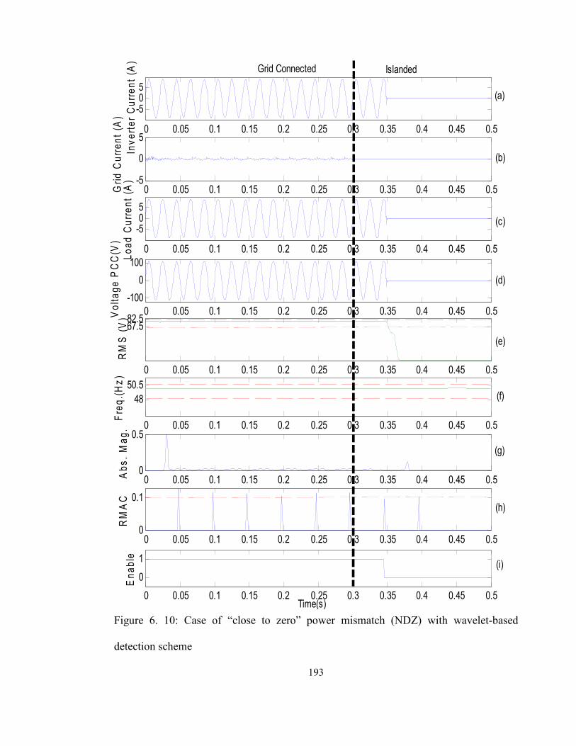
193
0 0.05 0.1 0.15 0.2 0.25 0.3 0.35 0.4 0.45 0.5
-505
Inv
ert
er
Cu
rre
nt
(A)
0 0.05 0.1 0.15 0.2 0.25 0.3 0.35 0.4 0.45 0.5-5
0
5
Gri
d C
urr
en
t (A
)
0 0.05 0.1 0.15 0.2 0.25 0.3 0.35 0.4 0.45 0.5
-505
Lo
ad
Cu
rre
nt
(A)
0 0.05 0.1 0.15 0.2 0.25 0.3 0.35 0.4 0.45 0.5
-100
0
100
Vo
lta
ge
PC
C(V
)
0 0.05 0.1 0.15 0.2 0.25 0.3 0.35 0.4 0.45 0.5
67.582.5
RM
S (
V)
0 0.05 0.1 0.15 0.2 0.25 0.3 0.35 0.4 0.45 0.5
48
50.5
Fre
q.(
Hz
)
0 0.05 0.1 0.15 0.2 0.25 0.3 0.35 0.4 0.45 0.50
0.5
Ab
s.
Ma
g.
0 0.05 0.1 0.15 0.2 0.25 0.3 0.35 0.4 0.45 0.50
0.1
RM
AC
0 0.05 0.1 0.15 0.2 0.25 0.3 0.35 0.4 0.45 0.5
0
1
Time(s)
En
ab
le
Grid Connected Islanded
(a)
(b)
(c)
(d)
(e)
(f)
(g)
(h)
(i)
Figure 6. 10: Case of “close to zero” power mismatch (NDZ) with wavelet-based
detection scheme

194
0 0.1 0.2 0.3 0.4 0.5
-100
0
100
Selected signal: 25 cycles. FFT window (in red): 5 cycles
Time (s)
0 200 400 600 800 10000
0.5
1
1.5
Frequency (Hz)
Fundamental (50Hz) = 108.8 , THD= 1.53%
Ma
g
0 0.1 0.2 0.3 0.4 0.5
-100
0
100
Selected signal: 25 cycles. FFT window (in red): 5 cycles
Time (s)
0 200 400 600 800 10000
0.2
0.4
0.6
0.8
1
1.2
1.4
Frequency (Hz)
Fundamental (50Hz) = 110.1 , THD= 0.57%
Ma
g
(a) Before islanding (b) After islanded
Figure 6. 11: Harmonic spectrum of the PCC voltage

195
6.3.5 Experimental results
In order to test this proposed technique experimentally on a real three-phase grid
connected inverter system using dSpace DS1104 DSP , experiments are carried out on
the 5.625 kW prototype that was built. Figure 5.27 of Chapter 5 shows the system
diagram with component values of the experimental setup and appropriate sensors used
for control purposes. The maximum sampling frequency achieved was fs=5 kHz. The
three cases seen for simulation are again verified by hardware experiments.
(a),(b),(c),(d),(e) and (f) in Figure 6.12, Figure 6.13 and Figure 6.14 represent: (a) grid
voltage (stepped down via transformer) ,(b) current flowing through phase A, (c) RMAC
of 3rd
level wavelet coefficients ,(d) wavelet based analysis(WBA) enable signal, (e)
inverter enable and (f) absolute values of 3rd
level wavelet coefficients
Figure 6.12 shows the experimental result of case 1 where a large mismatch of power
occurs after islanding and conventional passive techniques are able to detect the
situation. The islanding scenario is manually generated by opening the breaker (SW1) on
the grid side at 62.76s in Figure 6.12.
Figure 6.13 shows the result of case 2 where power mismatch after islanding (at 31.59s)
is very small and conventional passive techniques are unable to prevent islanding.
Figure 6.14 shows case 3 where the proposed wavelet based technique detects islanding
with a very low level of power mismatch which occurs at 29.5s. The wavelet based
scheme detects islanding within 2.5 cycles.

196
Figure 6. 12: Experiment result: Case of large power mismatch with passive method

197
Figure 6. 13: Experimental Result: Case of “close to zero” power mismatch (NDZ) with
passive method

198
Figure 6. 14: Result: Case of “close to zero” power mismatch (NDZ) with wavelet-based
detection scheme

199
6.4 Conclusion
Islanding situations need to be prevented with distributed generation for safety reasons
and to maintain the quality of power supplied to customers. The Chapter looked into
various passive and active islanding techniques in terms of their capability to reduce the
NDZ, significant strengths and weaknesses. The power mismatch between the load and
the PV (DG) was analysed to help better understand the islanding scenario. A large
mismatch of power shows the voltage at PCC drifting away from the nominal operating
range within few cycles but “close to zero” mismatch of power shows the voltage within
the nominal range, making it difficult to detect by OVP/UVP and OFP/UFP relays in a
passive environment. The proposed scheme operates on the PCC voltage measurement
and is able to detect the islanding condition within an average of 2.5 power frequency
cycles. To avoid nuisance tripping due to transient disturbances, which may result if
wavelet coefficient thresholds are used directly, a new parameter namely RMAC of the
3rd
level wavelet coefficients are proposed to detect the islanding condition. The results
presented clearly demonstrate the effectiveness of the proposed islanding detection
scheme even under the worst case scenario i.e. ‘close to zero’ power mismatch
condition. The experimental results match the simulation results in all cases as expected.
Only up to three levels of decomposition are required in the technique developed, and no
peak detector is being used. This reduces the burden on the processor and allows rapid
decisions to be taken in the event of grid failure. For best results, initial grid harmonic
voltage content information could be utilised to determine the most suitable level of
RMAC to indicate the islanding scenario. It can be noted that if the grid voltage is
completely harmonic free, the present method proposed will not work. However, in a
distributed network environment, this possibility is highly unlikely.

200
Chapter 7
7. CONCLUSION AND FUTURE WORK
7.1 Conclusion
The main objective of this research work was to improve the control and
operation of a three-phase photovoltaic grid connected inverter for enhanced
performance. Four major sections were identified for improvement where the detailed
research work and contributions have been highlighted within this thesis.
The objectives laid down for this PhD thesis have been successfully realized
through analysis, simulation and experimental investigations. As part of this research
activity a 5.625 kW prototype of a three-phase grid connected inverter has been
constructed and tested with the necessary interface circuits. Also, a three-phase grid
connected photovoltaic inverter simulation model has been built in Simulink which was
used to design the prototype and to develop new control solutions. The completion of the
three-phase grid connected inverter and the effectiveness of the proposed techniques has
been proved through numerous simulation and experimental results.
A thorough comparison of the dc-dc boost with voltage source inverter and the Z-
Source inverter has been reported. A design guide along with a clear understanding of
the working principles, equations and control methods for the Z-Source inverter has been
presented.
The proposed ac side P&O maximum power point tracking algorithm requires
only a small ac current sensor (dc sensor-less) compared to two large dc voltage and
current sensors required by the conventionally used P&O method. The proposed method

201
has been simulated and its effectiveness proved by comparing the results to the more
commonly used P&O method under the same conditions. The proposed method is
expected to present the same drawbacks faced by the conventionally used method during
photovoltaic panel shading and presence of multiple power peaks as discussed in [71];
but has the advantage of detecting the maximum power point using only inverter ac
current. Furthermore this technique seems well suited for controlling the boost stage of
both dc-dc boost with VSI and Z-Source inverters in order to track the MPP. Unlike in
the conventional P&O method no continuous perturbation of power is required, so there
is no oscillating voltage that requires additional software filtering.
The novel passive islanding detection scheme proposed using wavelet analysis
has been demonstrated in simulation and experimentally on the hardware prototype. The
satisfactory disabling of the inverter within 2.5 to 5 power cycles during grid failure has
been demonstrated using both simulation and experimental results. The proposed scheme
is designed to work during very small mismatch of the power between the DG and the
load bringing the non detection zone close to zero. The presence of fifth and seventh
harmonics during the availability of grid voltage and the absence of these harmonic
contents at inverter output after the grid has failed, has been utilized for anti islanding
protection using wavelets. The islanding protection scheme proposed along with the
UVP/OVP/UFP/OFP, dc link protection and over current protection have been tested and
prove sufficient for overall inverter protection during islanding and non islanding
conditions.
A working prototype of a three-phase grid connected inverter was developed to
demonstrate the new techniques and the performance of the hardware and control

202
algorithms met our design targets. The dc link controller and the three-phase software
PLL performed very well.
It is hoped that the theoretical and the experimental investigations reported in
this thesis will help in establishing new designs and control schemes for grid connected
inverters. It is further hoped that application engineers will be able to utilize the concept
and results reported in this thesis for further enhancement of the operation and control of
grid connected inverters under real photovoltaic and adverse grid supply conditions.

203
7.2 Future work
There are several important points, which need to be investigated but could not be
included in this current research work. The following issues have been identified as
some possible topics for future work in this area:
1. The control of the inverter can be extended to realize a current controlled strategy
rather than voltage control and also blanking time compensation could be
investigated.
2. Further testing could be carried out comparing the conventional and the proposed
ac side P&O MPPT algorithm in Chapter 3 under real PV and DSP
implementation to validate their effectiveness under normal and shading
conditions. Also the proposed scheme could be investigated with different grid
conditions, as ac current is used for tracking the MPP.
3. Further studies could be carried out to utilise the analysis of the proposed wavelet
based technique in Chapter 6. The inverter control algorithm could be modified
to operate in both active and reactive power transfer mode so that the PV inverter
could provide var compensation and local voltage support (needs to comply with
the future standards).
4. The developed system can be extended for micro grid applications, where the
inverter can run both in stand alone and in grid connected mode.

204
References
[1] M. Jamil,; B. Hussain,; M. Abu-Sara,; R.J. Boltryk,; S.M. Sharkh,; , "Microgrid
power electronic converters: State of the art and future challenges," Universities
Power Engineering Conference (UPEC), 2009 Proceedings of the 44th
International , vol., no., pp.1-5, 1-4 Sept. 2009
[2] M. H. Rashid, “Power Electronics Hand Book”, Academic Press, 2001
[3] IEEE Standard 929-2000, Recommended Practice for Utility Interface of
Photovoltaic (PV) Systems, IEEE, Inc., New York, NY, January 2000.
[4] IEEE Standard 1547-2003, Standard for Interconnecting Distributed Resources
with Electric Power Systems, IEEE, Inc., New York, NY, July 2003.
[5] EN50438, Requirements for the connection of micro-generators in parallel with
public low-voltage distribution networks, European Committee for Electro
technical Standardization, December 2007.
[6] F. Z. Peng and Y. Huang, “Z-Source inverter for power conditioning and utility
interface of renewable energy sources”, Michigan State University.
[7] [Online],Available: www.worldenergy.org, accessed: 15/02/2008
[8] Photovoltaics: Solar Electricity and Solar Cells in Theory and Practice, [Online].
Available:http://193.140.122.139/solar/resources/e-
books_and_papers/Solar%20Electricity%20and%20Solar%20Cells%20in%20Th
eory%20and%20Practice_%20Photovoltaics.pdf
[9] J.P. Thorton, “The effect of sand-storm on photovoltaic array and components”,
Solar energy conference, 1992

205
[10] R. Teodorescu, M. Liserre, P. Rodríguez, “Grid Converters for Photovoltaic and
Wind Power Systems”, Wiley, 2011
[11] S. Liu, “Maximum Power Point Tracker Model”, control model, University of
South Carolina, May 2000, Available :http://vtb.engr.sc.edu/modellibrary_old
[12] G. Hille, W. Roth and H, Schmidt, “Photovoltaic System”, in Fraunhofer
Institute for Solar Energy Systems. Friburg, Germany, 1995
[13] V. Arcidiacono, S. Corsi and L larnhri, “Maximum Power point tracker for
photovoltaic power plants”, presented at Proc. IEEE Photovoltaic’s Specialists
Conf.,1982
[14] M.H. Rashid, “Power Electronics : Circuits, Devices and Applications”, 2nd Ed.,
Prentice Hall, 1993
[15] C. Jaen, et al., "Overview of maximum power point tracking control techniques
used in photovoltaic systems." in Electronics, Circuits and Systems, ICECS 15th
IEEE International Conference, 2008.
[16] T. Kerekes, R. Teodorescu, M. Liserre, R. Mastromauro and A. Dell’Aquila,
“MPPT algorithm for voltage controlled PV inverters”OPTIM 2008, 11th
International Conference on Conference, on page(s): 427-432, 22-24 May 2008.
[17] S.M. Abu-Sharkh,; Z.F. Hussien,; J.K. Sykulski,; , "Current control of three-
phase PWM inverters for embedded generators," Power Electronics and
Variable Speed Drives, 2000. Eighth International Conference on (IEE Conf.
Publ. No. 475) , vol., no., pp.524-529, 2000

206
[18] M. Liserre, R. Teodorescu, F. Blaabjerg “Stability of Grid-Connected PV
Inverters with Large Grid Impedance Variation”, 35th Annual IEEE Power
Electronics Specialists Conference, 2004
[19] M. Liserre, F. Blaabjerg, et al, "Grid Impedance Estimation via Excitation of
LCL -Filter Resonance." Industry Applications, IEEE Transactions on 43(5):
1401-1407, 2007.
[20] M. Liserre, R. Teodorescu, et al, "Stability of photovoltaic and wind turbine
grid-connected inverters for a large set of grid impedance values." Power
Electronics, IEEE Transactions on 21(1): 263-272, 2006
[21] ANSI/IEEE C84.1 – 1995, American National Standard for Electric Power
Systems and Equipment - Voltage Ratings (60 Hertz)
[22] IEEE 519 – 1992, Recommended Practices and Requirements for Harmonic
Control in Electrical Power Systems
[23] UL 1741, Standard for Safety Inverters, Converters, Controllers and
Interconnection System Equipment for Use With Distributed Energy Resources,
May 1999.
[24] [Online],Available:http://www.esb.ie/esbnetworks/downloads/conditions_govern
ing_the_connection_and_operation_of_microgeneration_131106.pdf , accessed :
02/02/2010
[25] [Online],Available:http://www.cohortviii.com/~matthes/projects/boost_conv.pdf,
accessed: 06/06/2009

207
[26] “Z-Source Inverter for fuel Cell Vehicles”, paper prepared by Michigan State
University, Program manager: Mitch Olszewski for Oak Ridge National
Laboratory, for the U.S. DEPARTMENT OF ENERGY, September 2005.
[27] M. Shen, A. Joseph, J. Wang, F.Z. Peng, D.J. Adams ,”Comparison of traditional
inverters and Z-source inverter for fuel cell vehicles”
IEEE Transactions on PowerElectronics, Volume 22, Issue 4, Page(s):1453 –
1463, July 2007
[28] B.Farhangi, S. Farhangi, “Comparison of z-source and boost-buck inverter
topologies as a single phase transformer-less photovoltaic grid-connected power
conditioner”, Power Electronics Specialists Conference, 2006. 37th IEEE PESC
'06, Page(s):1 – 6, 18-22 June 2006
[29] A. Kulka, T. Undeland, “Voltage Harmonic Control of Z-source Inverter for UPS
Applications”, Power Electronics and Motion Control Conference, 2008. EPE-
PEMC 2008 13th, Page(s):657 – 662, 1-3 Sept. 2008
[30] Q.V Tran, T.W. Chun, J. R Ahn and H. H. Lee, “Algorithms for controlling both
the DC Boost and AC Output Voltage of Z-Source Inverter”, IEEE Transactions
on Power Electronics, Page(s):2745 – 2750,Oct. 2007.
[31] P. Xu, X. Zhang; C.W. Zhang; R.X. Cao; L. Chang, “Study of Z-Source Inverter
for Grid-Connected PV Systems”, Power Electronics Specialists Conference,
page(s): 1-5, 37th IEEE PESC '06.
[32] F. Z. Peng, “Z-Source Inverter,” IEEE Transactions on Industry Applications,
39(2), pp.504–510, March/April 2003.

208
[33] M. Shen, A. Joseph, H. Yi, F.Z. Peng, Z. Qian, “Design and Development of a
50kW Z-Source Inverter for Fuel Cell Vehicles” Power Electronics and Motion
Control Conference, page(s): 1-5, CES/IEEE 5th International IPEMC '06.
[34] K. Rajashekara, “Power Conversion and Control Strategies for Fuel Cell
Vehicles,” in Proc. Industrial Electronics Society, 2003, vol. 3, pp. 2865- 2870,
Nov. 2003.
[35] K. Holland, M. Shen, F.Z. Peng, “Z-source inverter control for traction drive of
fuel cell - battery hybrid vehicles” record of IEEE Industry Applications
Conference, 2005 Volume 3, 2-6, pp.1651 – 1656, October 2005.
[36] M. Shen, J. Wang, A. Joseph, F. Z. Peng, L. M. Tolbert, and D. J. Adams,
“Maximum constant boost control of the Z source inverter,” in Proceedings,
page: 147, IEEE IAS ’04, 2004.
[37] F. Z. Peng, M. Shen, Z. Qian, “Maximum boost control of the Z-source inverter,”
IEEE Transactions on Power Electronics, volume: 20(4), Page(s):833 – 838,
July 2005.
[38] B. J. Rabi, R. Arumugam,“Harmonics study and comparison of Z-Source
Inverter with traditional Inverters”, American Journal of Applied Sciences,
pages: 1418-1426, 2005
[39] F. Z. Peng; A. Joseph,; J. Wang; M. Shen, et al. , "Z-source inverter for motor
drives," Power Electronics, IEEE Transactions on , vol.20, no.4, pp. 857- 863,
July 2005

209
[40] M. Prodanovic, T. C. Green, “Control and Filter Design of Three-Phase Inverters
for High Power Quality Grid Connection,” IEEE Trans on Power Electronics,
Vol.8, No.1, pp. 373-380, January 2003
[41] A. Durgadevi,; S. Arulselvi,; S.P. Natarajan,; , "Study and implementation of
Maximum Power Point Tracking (MPPT) algorithm for Photovoltaic systems,"
Electrical Energy Systems (ICEES), 2011 1st International Conference on , vol.,
no., pp.240-245, 3-5 Jan. 2011
[42] L.G. B. Rolim, “Novel Control Stratergy for grid-Connected DCAC Converters
with Load Power Factor and MPPT Control”, [Online]. Available:
http://www.solar.coppe.ufrj.br/rolim.html
[43] S. Masri , P.W. Chan, "Design and development of a DC-DC boost converter
with constant output voltage," Intelligent and Advanced Systems (ICIAS), 2010
International Conference on , vol., no., pp.1-4, 15-17 June 2010
[44] S. K. Kim, et al., “Modeling and simulation of a grid-connected PV generation
system for electromagnetic transient analysis “,Volume 83, Issue 5, Pages 664-
678, May 2009
[45] “Control of Power Conversion Systems for the intentional islanding of
distributed generation units” Msc Thesis, Timothu N. Thacker
[46] Z. Ye; et al, “Evaluation of Anti-Islanding Schemes based on Nondetection Zone
Concept”, IEEE Transactions on Power Electronics, Vol: 19, Issue: 5, Sept 2004

210
[47] S.I. Jang.; K.H. Kim, “An Islanding Detection Method for Distributed
Generations using Voltage Unbalance and Total Harmonic Distortion of
Current”, IEEE Transactions on Power Delivery, Vol: 19, Issue: 2, Pages 745-
752, April 2004
[48] S.I. Jang.; K.H. Kim, “Development of a Logical Rule-Based Islanding
Detection Method for Distributed Resources”, IEEE Power Engineering Society
Winter Meeting, Vol: 2, Pages 800 – 806, Jan 2002
[49] C. Jeraputra; P.N. Enjeti, “Development of a Robust Anti-Islanding Algorithm
for Utility Interconnection of Distributed Fuel Cell Powered Generation”, IEEE
Transactions on Power Electronics, Vol: 19. Issue 5, Sept 2004
[50] C. Jeraputra; et al, “An Improved Anti-Islanding Algorithm for Utility
Interconnection of Multiple Distributed Fuel Cell Powered Generations”, IEEE
Applied Power Electronics Conference, Vol: 1, March 2005
[51] J.E. Kim; J.S. Hwang, “Islanding Detection Method of Distributed Generation
Units Connected to Power Distribution System”, International Conference on
Power System Technology, Vol: 2, Dec 2000
[52] Z. Ye; et al, “A New Family of Active Antiislanding Schemes based on DQ
Implementation for Grid-Connected Inverters”, IEEE Power Electronics
Specialists Conference, Vol: 1, June 2004
[53] O. Abarrategui, I. Zamora “Comparative analysis of Islanding Detection
methods in networks with DG”, 19th International Conference on Electricity
Distribution, Vienna, 21-24 May 2007

211
[54] M. Xu, , R. V. N. Melnik, et al. (2004). "Modeling anti-islanding protection
devices for photovoltaic systems." Renewable Energy 29(15): 2195-2216, Dec
2004
[55] J. Kim,; J. Kim,; Y. Ji,; Y. Jung,; C.Won,; , "An Islanding Detection Method for
a Grid-Connected System Based on the Goertzel Algorithm," Power Electronics,
IEEE Transactions on , vol.PP, no.99, pp.1, 2011
[56] W.Y Chang; , "An Islanding Detection Method for Grid-Connected Inverter of
Distributed Renewable Generation System," Power and Energy Engineering
Conference (APPEEC), 2011 Asia-Pacific , vol., no., pp.1-4, 25-28 March 2011
[57] P. K. Ray, S. R. Mohanty, et al. "Disturbance detection in grid connected
distributed generation system using wavelet and S-transform." Electric Power
Systems Research 81(3): 805-819.
[58] J. Stevens, R. Bonn, J. Ginn, S. Gonzalez, G. Kern, “Development and Testing
of an Approach to Anti-Islanding in Utility-Interconnected Photovoltaic
Systems,” Tech Rep., Sandia National Laboratories, Albuquerque, NM, August
2000.
[59] W. Bower and M. E. Ropp, “Evaluation of Islanding Detection Methods for
Photovoltaic Utility-Interactive Power Systems,” Tech Rep. IEA PVPS T5-
09:2002, [Online] Available: http://www.iea-pvps.org, 2002.
[60] D.Velasco, C. L. Trujillo, et al. "Review of anti-islanding techniques in
distributed generators." Renewable and Sustainable Energy Reviews 14(6):
1608-1614,August 2010

212
[61] M. Hanif, M. Basu and K. Gaughan,: “A Discussion of Anti-islanding Protection
Schemes Incorporated in a Inverter Based DG”, International Conference on
Environment and Electrical Engineering (EEEIC) 2011, 10th
International, 8-11
May 2011
[62] U. D. Dwivedi, and S. N. Singh, “Enhanced Detection of Power Quality Events
Using Intra and Inter-Scale Dependencies of Wavelet Coefficients”, IEEE Trans.
Power Delivery vol. 25, no. 1, pp. 358-366, Jan. 2010.
[63] U. D. Dwivedi, and S. N. Singh, “De-noising Techniques with Change-Point
Approach for Wavelet-Based Power Quality Monitoring” IEEE Trans. on Power
Delivery vol. 24, no. 3, pp. 1719-1727, July 2009.
[64] U. D. Dwivedi, S. N. Singh, and S. C. Srivastava, “A Wavelet based Approach
for Classification and Location of Faults in Distribution Systems”, IEEE Conf. &
Exhibition on Control, Communication and Automation (INDICON ) , India,
vol. 2 pp. 488–493, Dec. 11-13, 2008.
[65] I. Daubechies “The wavelet transforms, time frequency localization and signal
analysis,” IEEE Trans. IT, vol.36, no.5, pp. 961-1005, Sep. 1990.
[66] S. Mallat, “A theory for multi-resolution signal decomposition the wavelet
representation,” 1EEE Trans. Pattern Analysis and Machine Intelligence, vol.
11, no. 7, pp. 674-693, 1989.
[67] M. Basu and B. Basu, “Application of Wavelet Transform to Power Quality
(PQ) Disturbance Analysis”, Proceedings of Power Electronics and Machine
Drives, Edinburgh, 31st March – 2nd April, , pp. 269-273, PEMD 2004.
213
[68] A. Pigazo, , M. Liserre, et al. (2009). "Wavelet-Based Islanding Detection in
Grid-Connected PV Systems." Industrial Electronics, IEEE Transactions on
56(11): 4445-4455
[69] C.T. Hsieh, J.-M. Lin, et al. (2008). "Enhancement of islanding-detection of
distributed generation systems via wavelet transform-based approaches."
International Journal of Electrical Power & Energy Systems 30(10): 575-580
[70] S.J. Huang, C.T. Hsieh, Coiflet wavelet transform applied to inspect power
system disturbances-generated signals, IEEE Trans. Aero Electron. Syst. 38
(1)(2002) 204–210.
[71] R. Kadri,; J.P Gaubert ; G. Champenois,; , "An Improved Maximum Power Point
Tracking for Photovoltaic Grid-Connected Inverter Based on Voltage-Oriented
Control," Industrial Electronics, IEEE Transactions on , vol.58, no.1, pp.66-75,
Jan. 2011
[72] K. Latham, Master Thesis on ‘Solar Electric Systems Installed in 16 California
Municipalities’2004,[Online]Available:http://lomaprieta.sierraclub.org/global_w
arming/PVMuniThesis2.pdf
[73] M. E. Ropp, “Design Issues for Grid-Connected Photovoltaic Systems,” Ph.D.
dissertation, Georgia Institute of Technology, Atlanta, GA, 1998.
[74] TMS320F2812 User Manual
[75] dSPace DS1104 User Manual
[76] [Online] Available: www.sei.ie, accessed: 15/06/2009

214
[77] N.A. Rahim, J. Selvaraj, and Krismadinata. “Hysteresis Current Control and
Sensor-less MPPT for grid-Connected Photovoltaic Systems.” in Industrial
Electronics, 2007. ISIE 2007. IEEE International Symposium on. 2007
[78] A. Pigazo, V. M. Moreno, et al. "Wavelet-Based Islanding Detection Algorithm
for Single-Phase Photovoltaic (PV) Distributed Generation Systems." IEEE
International Symposium on Industrial Electronics, ISIE 2007.
[79] M. Hanif,; U.D. Dwivedi,; M. Basu,; K. Gaughan,; , "Wavelet based islanding
detection of DC-AC inverter interfaced DG systems", Universities Power
Engineering Conference (UPEC), 2010 45th International , vol., no., pp.1-5,
Aug. 31 2010-Sept. 3 2010
[80] M.A. Abusara,; S.M. Sharkh,; , "Design of a robust digital current controller for
a grid connected interleaved inverter," Industrial Electronics (ISIE), 2010 IEEE
International Symposium on , vol., no., pp.2903-2908, 4-7 July 2010
[81] I. Axente, “Unified Power Quality Conditioner: protection and performance
enhancement” PhD Thesis, Dublin Institute of Technology, Ireland, 2008
[82] J. N. Ganesh, “Unified power quality conditioner for grid integration of wind
generators”, PhD Thesis, Dublin Institute of Technology, Ireland, 2008

215
crea
te 3
phas
e
lead
ang
le in
radi
ans
inpu
t
sine
pk
, chn
ages
M
norm
alis
ed 3
pha
se
wt
feed
bac
k of
cur
rent
, rm
s us
ed
V in
vert
er L
L &
LN
,
& I
flow
ing
V g
rid
L-N
& I
flow
ing
*for
cur
rent
, gai
nx10
is u
sed
note
: cur
rent
pea
k/ r
oot 2
= rm
s am
ps
vdc
VLL
bef
or fi
lter
VLL
A-B
aft
er fi
lter
VLn
A-N
aft
er f
ilter
ILin
e
V g
rid
l-n
2.43
A*2
30V
= 1
680W
out
put
dc-d
c 16
80/7
80V
=2.
15A
dc-d
c R
out
= 78
0/2.
15 =
362o
hms
400V
in, 7
80 V
out
, d=4
9%
inve
rter
pw
m fr
eq =
2k H
z
sim
ulin
k sa
mpl
in fr
eq =
125
k H
z
dc-d
c fr
eq =
2k
ther
efor
e L=
(1-d
^2)d
R/2
f
C=d
Vou
t/V
rRf
PV
pow
er
Pow
er in
to th
e D
C-D
C
340
0W P
V
max
I re
f nee
ds to
be
chan
ged
with
PV
cur
ve
250H
z C
urre
nt c
ontr
olle
r
50%
ini
tial D
cyc
le
grid
dis
conn
ect
0.4s
step
0.0
1
1700
W P
V
50H
z M
PPT
cont
roll
er
PV
pow
er s
hift
s at
0.1
s
LC
toge
ther
with
RL
bran
ch=>
LC
L fi
lter
R=0
.6, L
=7,5
mH
, C=1
0uF
R=0
.6, L
=7,5
mH
sync
hron
ize
1
780
pow
ergu
i
Dis
cret
e,
Ts =
8e-
006 s
grid
tem
plat
e 3-
phas
e gr
id
3-ph
ase
grid
nor
mal
ised
3-ph
ase
rms
V
3-ph
ase
peak
V
Vol
tage
Mea
sure
men
t9
v+ -
Vol
tage
Mea
sure
men
t6
v+ -
Vol
tage
Mea
sure
men
t5
v+ -
Vol
tage
Mea
sure
men
t4
v+ -
Vol
tage
Mea
sure
men
t3
v+ -
Vol
tage
Mea
sure
men
t2
v+ -
Vol
tage
Mea
sure
men
t10
v+ -
Vol
tage
Mea
sure
men
t1
v+ -
Vol
tage
Mea
sure
men
t
v+ -
Uni
vers
al B
ridg
e
g A B C
+ -
Uni
t Del
ay2
z1
Uni
t Del
ay1
z1
Uni
t Del
ay
z1
Tran
sfer
Fcn
80
2s+8
0
To W
orks
pace
sim
out
Thre
e-P
hase
Sou
rce
N
A B C
Thre
e-P
hase
Bre
aker
A B C
a b c
Thre
e-P
hase
Seri
es R
L B
ranc
h
A B C
A B C
Switc
h
Seri
es R
Bra
nch
Scop
e6
Scop
e5
Scop
e3Sc
ope2
Scop
e19
Scop
e15
Scop
e11
Scop
e10
Scop
e1
SPW
M G
ener
atio
n
Sine
Ref
s
boos
t dut
y cy
cle
ref
6 IN
V P
WM
boos
t PW
M
Rep
eatin
g
Sequ
ence
2
Rep
eatin
g
Sequ
ence
1
RTI
Dat
a
Prod
uct2
Prod
uct1
PV lo
okup
V in
put,
I ou
tput
2
PV lo
okup
V in
put,
I ou
tput
1
PV lo
okup
V in
put,
I ou
tput
Mul
tim
eter
1
6
Mul
tim
eter
1
MPP
T
DC PowerBoost D Ref
LC
Fil
ter
A B C C 1
A
B C
L
IGB
T
g m
C E
Gai
n2
10
Gai
n110
Dis
cret
e
PI C
ontr
olle
r1
PI
Dis
cret
e
3-ph
ase
PLL
1
Vab
c (p
u)
Freq
wt
Sin_
Cos
Dio
de
ma
k
DC
link
err
or
DC
Lin
k co
ntro
llerV
cap
In2
Iref
Cur
rent
Mea
sure
men
t3
i+
-
Cur
rent
Mea
sure
men
t2
i+
-
Cur
rent
Mea
sure
men
t1
i+
-
Cur
rent
Mea
sure
men
t
i+
-
Con
trol
led
Cur
rent
Sou
rce
s
-+
Clo
ck0
Cal
c M
& d
elta
Grid
rm
s V
& I
rm in
ject
ed Vdc
lead
ang
le in
rai
dans
pk o
f si
ne w
ave
. for
M
C
3.2
kW
ABC
3-Ph
ase
refe
renc
e ge
nera
tor
wt
delta
sine
pea
k fo
r M
3 re
f Si
nes
Ap
pen
dix
1:
Th
ree
ph
ase
gri
d c
on
nec
ted
PV
sy
stem
wit
h P
&O
MP
PT

216
pk
of
inve
rte
r vo
ltag
e
lea
d a
ng
le i
n r
aid
an
s
pk
if
sin
e w
ave
fo
r M
pk
of
sin
e w
ave
. fo
r M
2
lea
d a
ng
le i
n r
aid
an
s
1
ca
lcu
late
s=
> (
rms
in
vert
er
volta
ge
) *
roo
t 2
= c
alc
ula
tes
pe
ak
in
vert
er
vola
tge
f(u
)
ca
lcu
late
s le
ad
an
gle
in
ra
dia
ns
f(u
)
ca
lcu
late
s
(sin
e p
k)
to m
od
ify
M,
vdc
= 7
80
f(u
)
Sc
op
e1
7
Vd
c
2
Gri
d r
ms
V &
Irm
in
jec
ted
1
Bo
ost
D R
ef
1
Uni
t De
lay
4z1
Uni
t De
lay
3z1
Sco
pe
4
MP
PT
u
Pold
y
y1
Pold1
MP
PT
Ena
ble
AC
Cur
rent
1
wt+
de
lta
3 r
ef
Sin
es
1
sin
(u(1
)-2
*pi/
3)
f(u
)
sin
(u(1
))
sin
(u(1
))
Sc
op
e
Pro
du
ct1
Ad
d3
Ad
d2
sin
e p
ea
k f
or
M
3
de
lta2wt
1
A
.1.1
:Cal
c M
& d
elta
su
bsy
stem
A.1
. 2:
MP
PT
(su
bsy
stem
)
A.1
.3:
3-P
has
e re
fere
nce
gen
erat
or
subsy
stem

217
2k
Hz
tra
ing
le,
am
p +
6 t
o+
6
ca
rrie
r is
-6
to
+6
ref
at
-6 g
ive
s D
=0
ref
at
0 g
ive
s D
=5
0%
ref
at
6 g
ive
s D
=1
00
%
bo
os
t P
WM
26
INV
PW
M
1
Tri
an
gle
Sc
op
e8
Sc
op
e2
Sc
op
e1
Sc
op
e
>=>
=
Lo
gic
al
Op
era
tor
NO
T
Da
ta T
ype
Co
nve
rsio
n1
do
ub
le
Da
ta T
ype
Co
nve
rsio
n
do
ub
le
bo
os
t d
uty
cyc
le r
ef
2
Sin
e R
efs
1
A.1
.4:
SP
WM
Gen
erat
ion s
ubsy
stem
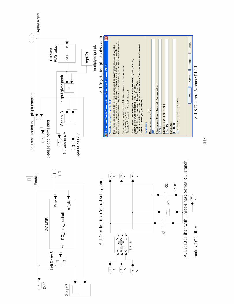
218
Out
1
1
Uni
t De
lay
5
z1
Sco
pe
7
DC
LIN
K
Vc
ap
Ire
f_o
ld
Ire
fD
C_
Lin
k_
cont
rolle
r
Ena
ble In
11
3-p
ha
se
pe
ak
V
3
3-p
ha
se
rm
s V
2
3-p
ha
se
gri
d n
orm
alis
ed
1
ou
tpu
t g
ive
s p
ea
k
mu
ltip
ly t
o g
et
pk
sq
rt(2
)
inp
ut
sin
e s
ca
led
to
1
pk
-pk
te
mp
late
Sc
op
e1
3
Dis
cre
te
RM
S v
alu
e InR
MS
3-p
ha
se
gri
d
1
10
uF
C 17
C 6B 5A
4
C3B2A1
Cf2
Cf1
Cf
7.5
mH
A B C
A B C
A.1
.5:
Vdc
Lin
k C
ontr
ol
subsy
stem
A
.1.6
: gri
d t
empla
te s
ubsy
stem
A.1
.7:
LC
Fil
ter
wit
h T
hre
e-P
has
e S
erie
s R
L B
ran
ch
mak
es L
CL
fil
ter
A.1
.8 D
iscr
ete
3-p
has
e P
LL
1

219
10k
Hz t
rain
gle
, am
p -10
to +
10
V
ILo
ad
VL
IL IC VC
Vlo
ad
Sin
wav
e1,4
an
d 5
are
no
t used
, can b
e u
sed t
o t
est
3rd
ham
on
ic in
jecti
on i
f n
ecessary
po
werg
ui
Dis
cre
te,
Ts =
1e-0
07
s
Vo
ltage M
easu
rem
en
t
v+ -
Univ
ers
al
Bri
dge
g A B C
+ -
Tri
an
gle
Th
ree-
Ph
ase
Seri
es R
Bra
nch
A B C
A B C
Sin
e W
ave5
Sin
e W
ave4
Sin
e W
ave3
Sin
e W
ave2
Sin
e W
av
e1
Sin
e W
ave
Sco
pe8
Sco
pe2
Sco
pe1
0
Sco
pe1
Sco
pe
>=
Pu
lse
Gen
era
tor
57%
Mu
ltim
ete
r1
6
Lo
gic
al
Opera
tor
NO
T
LC
Filte
r
A B C
A
B
C
L
IGB
T
g m
C E
Dio
de
ma
k
Data
Ty
pe C
on
vers
ion1
do
ub
le
Data
Ty
pe C
on
vers
ion
do
uble
DC
Volt
age S
ou
rce
40
0V
C
Ap
pen
dix
2:
dc-
dc
bo
ost
wit
h V
SI

220
ILoa
dIL
1V
L1IC
1V
C1V
C2V
L2V
Loa
d
1680
W/3
=560
W=
230V
*2.
43A
, R=9
4.5o
hms
pow
ergu
i
Dis
cret
e,T
s = 1
e-00
7 s
Vol
tage
Mea
sure
men
t
v+ -
Thr
ee-P
hase
Ser
ies
Res
istiv
e L
oad
A B C
A B C
Sin
e(w
t-120
)
Sin
e(w
t)
Sin
(wt+
120)
Sho
ot-t
hrou
gh r
efer
ence
7.15
5
Sco
pe6
Sco
pe10
Sco
pe1
Pw
m G
ener
ator
Pha
se 1
Sin
e R
ef
Pha
se 2
Sin
e R
ef
Pha
se 3
Sin
e R
ef
Car
rier
Shoo
t-th
roug
h re
f
Gat
e Si
gnal
s
Mul
timet
er1
9 LC
Filt
er
A B C
A
B
C
L2L1
Inve
rter
Bri
dge
g A B C
+ -
Dio
de
DC
Vol
tage
Sou
rce
400V
C2
C1
10kH
z C
arri
er T
rain
gle
Ap
pen
dix
3:
Z-S
ou
rce
Inv
erte
r
221
Gate
Sig
nals
1
Sco
pe8
Scop
e5
Sco
pe4
Sco
pe3
Sco
pe2
Sco
pe1
Scop
e
>=
>=>
=
Lo
gic
al
Opera
tor
NO
T
Gain
-1
Data
Ty
pe C
onv
ers
ion1
do
ub
le
Data
Ty
pe C
on
vers
ion
do
ub
le
Add
1
Ad
d
Sh
oot-
thro
ugh
ref
5
Carr
ier
4
Ph
ase
3 S
ine R
ef
3P
hase
2 S
ine R
ef
2P
hase
1 S
ine R
ef
1
A.3
.1:
PW
M G
ener
ator
subsy
stem

222
crea
te 3
phas
e
lead
ang
le in
radi
ans
inp
ut
sine
pk
, chn
ages
M
norm
alis
ed
3 p
hase
wt
feed
bac
k of
cur
rent
, rm
s us
ed
V in
vert
er L
L &
LN
,
& I
flow
ing
V g
rid L
-N &
I flo
win
g
*for
cur
rent
, gai
nx10
is u
sed
note
: cur
rent
pea
k/ r
oot 2
= rm
s am
ps
vdc
VLL
bef
or fi
lter
VLL
A-B
afte
r filt
er
VLn
A-N
afte
r filt
er
ILin
e
V g
rid l-
n
2.43
A*2
30V
= 1
680
W o
utp
ut
dc-d
c 16
80/7
80V
=2.
15
A
dc-d
c R
out
= 7
80/2
.15
=362
ohm
s
400
V in
, 780
V o
ut, d
=49
%
inve
rter p
wm
freq
=
2k H
z
sim
ulin
k sa
mpl
in fr
eq
= 12
5k
Hz
dc-d
c fr
eq =
2k
ther
efo
re L
=(1
-d^2
)dR
/2f
C=
dVou
t/VrR
f
PV
pow
er
Pow
er in
to th
e D
C-D
C
pow
er 3
400
W P
V
LC fi
lter=
=>
7.5
mH
& 1
0uF
max
ref
nee
d to
be
cha
nged
with
max
pow
er
250
Hz
curr
ent c
ontro
ller
50H
z M
PP
T co
ntro
ller
50%
initi
al D
cyc
le
po
we
r 17
00W
PV
sync
hron
ize
1
780
pow
ergu
i
Dis
cret
e,
Ts =
8e-
006
s
grid
tem
plat
e
3
-ph
ase
gri
d
3-p
has
e g
rid
norm
alis
ed
3-p
has
e r
ms
V
3-p
has
e p
eak
V
Vol
tage
Mea
sure
men
t9
v+ -
Vol
tage
Mea
sure
me
nt6
v+ -
Vol
tage
Mea
sure
me
nt5
v+ -
Vol
tage
Mea
sure
me
nt4
v+ -
Vo
ltage
Me
asur
eme
nt3
v+ -
Vol
tage
Mea
sure
men
t2
v+ -
Vol
tage
Mea
sure
men
t10
v+ -
Vol
tage
Mea
sure
men
t1
v+ -
Vol
tage
Mea
sure
men
t
v+ -
Vdc
Lin
k C
ontro
lIn1
In2
Out
1
Uni
vers
al B
ridge
g A B C
+ -
Uni
t Del
ay
5z1
Uni
t Del
ay1
z1
Uni
t Del
ay
z1
Tran
sfer
Fcn
80
2s+
80
Thre
e-P
hase
Sou
rce
N
A B C
Thre
e-P
hase
Bre
aker
A B C
a b c
Thre
e-P
hase
Ser
ies
R B
ranc
hA B C
A B C
Sw
itch
Ser
ies
R B
ranc
h
Sco
pe7
Sco
pe6
Sco
pe5
Sco
pe3
Sco
pe
2
Sco
pe19
Sco
pe15
Sco
pe11
Sco
pe10
Sco
pe1
SP
WM
Ge
nera
tion
Sin
e R
efs
boos
t du
ty c
ycl
e re
f
6 I
NV
PW
M
boos
t P
WM
Rep
eatin
g
Seq
uenc
e2
Rep
eatin
g
Seq
uenc
e1
RTI
Dat
a
Pro
duct
2
Pro
duct
1P
V lo
okup
V in
put,
I ou
tput
1
PV
look
up V
inpu
t, I
outp
ut
Mul
timet
er1
6
Mul
timet
er
1
MP
PT
AC CurrentBoost D Ref
LC F
ilter
A B C C 1
A
B
C
L
IGB
T
g m
C E
Gai
n2
-K-
Gai
n1
10
Dis
cret
e
RM
S v
alue In
RM
S
Dis
cret
e
PI C
ont
rolle
r1
PI
Dis
cret
e
3-p
hase
PLL
1
Vab
c (
pu)
Fre
q
wt
Sin
_C
os
Dio
de
ma
k
DC
link
err
or
Cur
rent
Mea
sure
men
t3
i+
-
Cur
rent
Mea
sure
men
t2
i+
-
Cur
rent
Mea
sure
men
t1
i+
-
Cur
rent
Mea
sure
men
t
i+
-C
ontro
lled
Cur
rent
Sou
rce
s
-
+
Clo
ck0
Cal
c M
& d
elta
Gri
d rm
s V
& Ir
m i
njec
ted
Vdc
lead
an
gle
in r
aida
ns
pk o
f si
ne w
ave
. fo
r M
C
3-P
hase
refe
renc
e g
ener
ato
r
wt
del
ta
sin
e p
eak
for
M
3 re
f Sin
esAp
pen
dix
4:
Th
ree
ph
ase
gri
d c
on
nec
ted
PV
sy
stem
wit
h n
ov
el A
C s
ide
P&
O M
PP
T

223
lead
angle
1,2
,3 in
rad
ian
s in
pu
t
M1,
M2,
M3
no
rmal
ised
3 p
has
e
wt
chan
ge
rms
inp
ut
of
sin
es 2
6.2
5ch
ange
in
itia
l rm
s in
pu
t 7
7ch
nag
e v
dc 3
00
chan
ge g
ain
7 to e
xact
rms
pu
t ac
tual
gri
d f
or
ant
isla
nd
ing
sch
eme
chan
ge v
oltag
e pro
tect
ion c
od
e: lim
its
& T
ch
nage
un
it d
elay
7 in
itia
l v
alu
e
choo
se w
hic
h d
etail
level and
ch
ange
th
resh
th
acc
ord
ingly
pu
t ac
tual
Vd
c
I an
d V
1,V
2,V
3 r
ms
Wav
elet
Bas
ed a
nti-isl
and
ing
det
ecti
on a
nd
con
tro
l
usi
ng 2
rd l
evel
det
ail
coeff
icin
ts
scop
e 8
giv
es a
vg
energ
y o
f co
effi
cie
nts
17
deg
lea
d c
orr
ecti
on
4.7k O
hm
s at
sen
sin
g cc
t
PL
L P
I co
ntr
olle
r[60 1
40
0]P
LL
Fre
q r
ou
nd
ed o
ff t
o 1d
.p,
inp
ut*
10-
>ro
un
d>
/10-
>
adc-
>M
EA
N->
gain
53<
--1
0<--
AD
C
13
6.4
10
91.
6
12
50-
25
00
Hz
62
5-1
25
0 H
z
31
2.5-
62
5 H
z
15
6.2
5-3
12.
5 H
z
0-1
56.
25 H
z
500
0Hz
u=
wavle
t co
effi
cie
nt (
c)
y=
abs
(c)
E=
su
m o
f y'
sj=
co
un
ter
E2=
E3=
Av
erag
e energ
y=S
qrt
(E-y
/N)
N=
64 s
ample
s
0.0
2->
360-
>2pi
no
rmal
ised
=>
gri
d v
olt
age
/ 1
08 c
onst
pk
chan
ge D
C L
ink v
olt
age p
rote
ctio
n c
ode:
lim
its
& T
ch
nag
e u
nit
del
ay8
init
ial
valu
e
DS
P E
nab
le
Fre
q.
Ph
ase
A r
ms
dc
link
vo
ltag
e
Ph
ase
B r
ms
Ph
ase
C r
ms
WB
A
Pro
tect
ion
En
able
pro
tect
ion a
fter
5 s
ecoo
nd
s
En
able
pas
s b
oo
st d
uty
ref
dis
able
pass
es 0
bo
ost
du
ty r
ef
50
Hz E
nab
le s
ignal
Vd
c link
bo
ost
du
ty r
ef
77
.8 a
nd
1
0 f
or
ds
pa
ce
7
78
Ou
t11
shif
t u
p b
y 0
.5
shif
t 0.
613
rms
curr
ent
5
pw
m s
top
bit1
0
pw
m s
top
bit
0
pow
ergu
i
Dis
cret
e,T
s =
0.0
002
sm
ean
rm
s p
has
a
InM
ean
grid
tem
pla
te 3
-phas
e gri
d
3-p
has
e gri
d n
orm
alis
ed
3-p
has
e rm
s V
3-p
has
e peak
V
curr
ent
0
corr
ecti
on
bo
ost
enable
1
0
bo
ost
en
able
0
Wav
elet
D
eco
mp
osi
tio
n
In1
Out3
Out4
Out5
Out6
Out7
Vec
tor
Sco
pe1
Tim
e
Vdc m
easu
rem
ent
30
0
Un
it D
ela
y9
1/z
Un
it D
ela
y8
1/z
Un
it D
ela
y7
1/z
Un
it D
elay6
1/z
Un
it D
elay3
1/z
Un
it D
elay2
1/z
Unit
Dela
y12
1/z
Un
it D
elay
11
1/z
Unit
Del
ay1
1/z
Un
buff
erT
erm
inat
or6
Ter
min
ato
r5
Term
inat
or4
Ter
min
ato
r3
Ter
min
ato
r1
Sw
itch
Su
bsy
stem
3
In1
Out
1
Su
bsy
stem
2
In1O
ut1
Sub
syst
em
In1
In2
In3
In4
In5
In6
In7
Sin
e W
ave
Sco
pe8
Sco
pe7
Sco
pe5
Sco
pe3
Scop
e2
Sco
pe1
9
Sco
pe1
4
Scop
e12
Sco
pe1
1
Sco
pe1
0
Scop
e1
Sco
pe
Ram
p1
RT
I D
ata
Hit
Cro
ssin
g1
Go
to
[A]
Gai
n8
0.0
17
453
Gai
n7
1/(7
7)
Gai
n577
8
Gain
4
77
8
Gai
n3 77
8
Gai
n13
13
64
Gai
n12
92
4
Gai
n10
104
Fro
m1
[A]
Em
bed
ded
MA
TL
AB
Fu
nct
ion
E1
E2
j1 u
y E
E3 j
sw
fcn1
Em
8
uy
fcn
Em
6
u T1
y TV
olt
age_
pro
tectio
n
Em
5
u T1
y TV
olt
age_
pro
tect
ion
Em
4
u T1
y TD
C_
Lin
k_V
oltage
_pro
tect
ion
Em
3
u T1
y TV
olt
age_
pro
tect
ion
Em
2
u T1
y T
Fre
q_pro
tect
ion
Dis
crete
T
ota
l H
arm
on
icD
isto
rsio
n
signa
lT
HD
Dis
crete
R
MS
phase
A c
urr
ent
InR
MS
Dis
crete
M
ean v
alu
e2
In Mean
Dis
cret
e
Mea
n v
alu
e1
InM
ean
Dis
cret
e3-
phas
e P
LL1
Vabc
(pu
)
Fre
q
wt
Sin
_C
os
DS
P E
nab
le0
DS
110
4SL
_D
SP_P
WM
3
Duty
cyc
le a
Duty
cyc
le b
Duty
cyc
le c
PW
M S
top
DS1
104S
L_D
SP_
PW
M
PW
M C
hanne
l 1
PW
M C
hanne
l 2
PW
M C
hanne
l 3
PW
M C
hanne
l 4
DS1
10
4MU
X_
AD
C
MU
X A
DC
DS1
104D
AC
_C
2
DA
C
DS1
10
4AD
C_C
8
AD
C
DS
110
4AD
C_
C7
AD
C
DS
110
4AD
C_
C6
AD
C
DS
110
4AD
C_
C5
AD
C
Cal
c M
& d
elta
Vdc
Gri
d r
ms
V &
Irm
inj
ect
ed
lead
angle
1 i
n r
aidan
s
pk o
f si
ne w
ave
. fo
r M
1
lead
angle
2 i
n r
aidan
s
pk o
f si
ne w
ave
. fo
r M
2
lead
angle
3 i
n r
aidan
s
pk o
f si
ne w
ave
. fo
r M
3
Bu
ffer
Bo
ost
D
0
3-P
has
e re
fere
nce
gen
erat
or
wt
delta
sine p
eak f
or
M
3 r
ef
Sin
es
2
0.6
13
17 d
egre
es
17
1 0.5
<>
<>
Ap
pen
dix
5:
So
ftw
are
co
ntr
ol
pro
gra
m r
un
on
dS
Pace
DS
110
4

224
wt+
del
tasi
n i
s *
by
0.5
0.5*
sin
* M
wtw
t d1
d2
M1
M2
3 r
ef S
ines
1
Sco
pe
Pro
du
ct2
Pro
du
ct1
Ad
d3
Ad
d2 A
dd
10.
5sin
(u(1
)-2*
pi/
3)
f(u
)
0.5s
in(u
(1))
f(u
)
sin
e p
eak
fo
r M
3
del
ta2wt1
A.5
.1:
3-P
has
e re
fere
nce
gen
erat
or
(contr
ol
pro
gra
m s
ubsy
stem
)

225
pk
of
inv
ert
er
vo
ltage
lead a
ngle
in
raid
an
s M
pk
of
inv
ert
er
vo
ltage
lead a
ngle
in
raid
an
s M
pk o
f in
vert
er
volt
age
lead a
ngle
in r
aid
ans
Mpk
of
sin
e w
ave.
fo
r M
3
6
lead a
ngle
3 in
raid
ans
5
pk o
f si
ne w
av
e. f
or
M2
4
lead a
ngle
2 in
raid
an
s
3
pk o
f si
ne w
av
e. f
or
M1
2
lead a
ngle
1 in
raid
an
s
1
calc
ula
tes=
> (rm
s in
vert
er
volt
age)
* roo
t 2
= c
alc
ula
tes
peak i
nv
ert
er
vo
latg
e3
f(u
)
calc
ula
tes=
> (rm
s in
vert
er
vo
ltage)
* roo
t 2
= c
alc
ula
tes
peak
in
vert
er
vo
latg
e2
f(u)
calc
ula
tes=
> (rm
s in
vert
er
vo
ltage)
* roo
t 2
= c
alc
ula
tes
peak
in
vert
er
vo
latg
e1
f(u)
calc
ula
tes
lead a
ngle
in r
ad
ians2
f(u
)
calc
ula
tes
lead a
ngle
in
rad
ian
s1
f(u)
calc
ula
tes
lead
angle
in
radia
ns
f(u)
calc
ula
tes
(sin
e p
k)
to m
od
ify
M, v
dc
3
u[1
]*2/u
[2]
calc
ula
tes
(sin
e p
k) to
mod
ify
M, vd
c2
u[1
]*2/u
[2]
calc
ula
tes
(sin
e p
k) to
mod
ify
M, vd
c1
u[1
]*2/u
[2]
Z t
eta
f(u)
Z M
od
f(u)
Sco
pe2
Sco
pe17
Sco
pe1
R 1.2L
15.
6
Enable
Gri
d r
ms
V &
Irm
inje
cte
d
2
Vd
c
1
Peak inverter voltage function 1=sqrt((((u[1]*u[6]*cos(u[5]*pi/180)+u[2])^2)+((u[1]*u[6]*sin(u[5]*pi/180))^2))*2)
Lead angle function 1= atan((u[1]*u[6]*sin(u[5]*pi/180))/((u[1]*u[6]*cos(u[5]*pi/180)+u[2])))
A.5
.2:
Cal
cula
te M
& d
elta
(co
ntr
ol
pro
gra
m s
ubsy
stem
)

226
3-phas
e pea
k V
3
3-ph
ase
rms
V
2
3-phas
e gr
id n
orm
alis
ed
1
outp
ut
gives
pea
k multip
ly t
o g
et p
k
-C-
Sco
pe1
3
Gai
n
1/108
Dis
cret
e R
MS
val
ue
InR
MS
Dis
cret
e M
ean v
alu
e
InM
ean
3-phas
e gr
id
1
Lo
gica
lO
per
ato
r1
AN
D
Dat
a T
ype
Co
nver
sion
Conv
ert
DS1
10
4DA
C_C
1
DA
C
Enab
le
In77In66
In55
In44
In33
In22
In11
A.5
.3:
gri
d t
empla
te (
con
trol
pro
gra
m s
ubsy
stem
)
A.5
.4:
Subsy
stem
(co
ntr
ol
pro
gra
m s
ubsy
stem
)
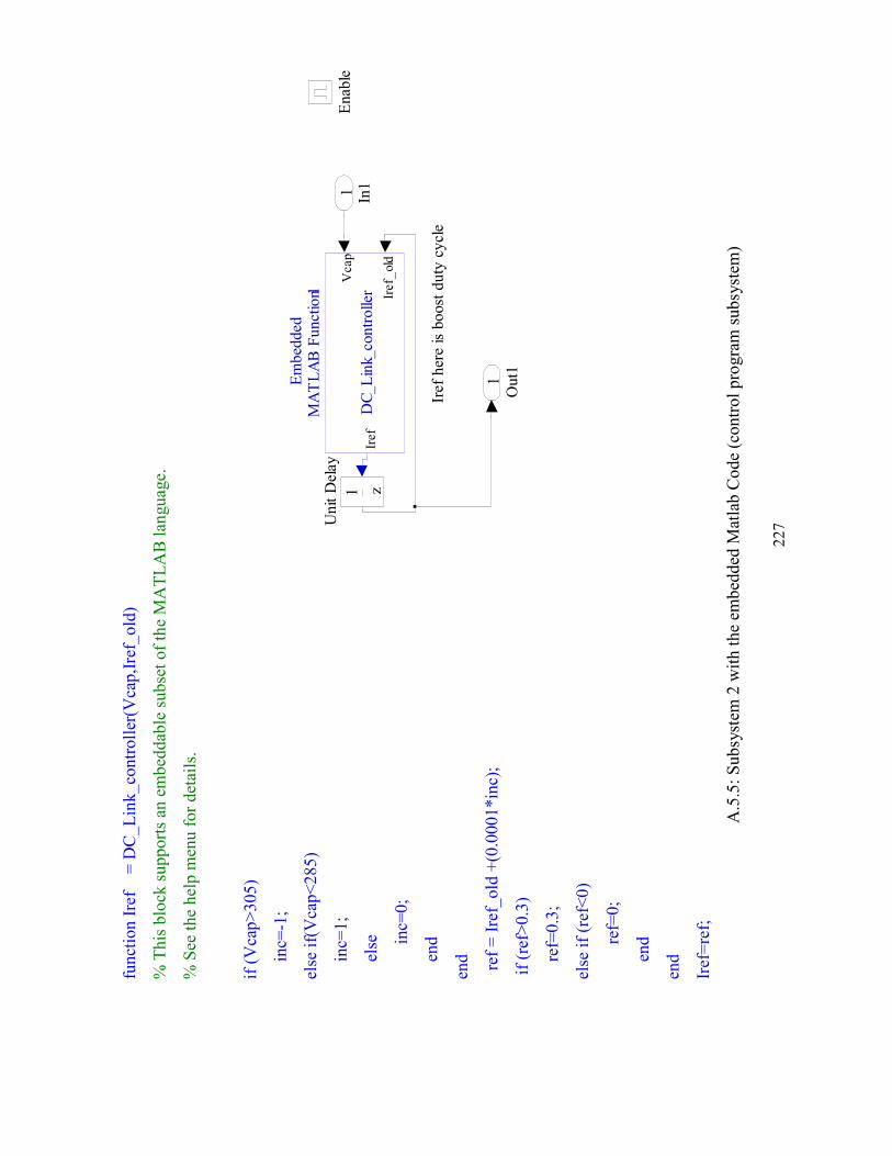
227
Iref
her
e is
bo
ost
du
ty c
ycl
e
Out11
Un
it D
elay
z1
Em
bed
ded
MA
TL
AB
Fu
nct
ion1
Vcap
Iref_
old
Iref
DC
_L
ink_
con
tro
ller
Enab
le
In11
funct
ion I
ref
=
DC
_L
ink_co
ntr
oll
er(V
cap,I
ref_
old
)
% T
his
blo
ck s
upport
s an
em
bed
dab
le s
ubse
t of
the
MA
TL
AB
lan
guag
e.
% S
ee t
he
hel
p m
enu f
or
det
ails
.
if (
Vca
p>
305)
in
c=-1
;
else
if(
Vca
p<
285
)
in
c=1;
el
se
in
c=0;
en
d
end
re
f =
Ire
f_old
+(0
.0001
*in
c);
if
(ref
>0.3
)
re
f=0.3
;
else
if
(ref
<0
)
re
f=0;
en
d
end
Iref
=re
f;
A.5
.5:
Subsy
stem
2 w
ith t
he
embed
ded
Mat
lab C
ode
(contr
ol
pro
gra
m s
ubsy
stem
)

228
Out11
Un
it D
elay
13
1/z
Em
7
u T1
y Tth
resh
Enab
leIn
11
funct
ion [
y,T
] =
thre
sh(u
,T1)
% T
his
blo
ck s
upport
s th
e E
mbed
ded
MA
TL
AB
subse
t.
% S
ee t
he
hel
p m
enu f
or
det
ails
.
y=
1;
T=
1;
th=
0.5
; %
thre
shold
% y
= u
;
if (
th>
u) %
on
ce t
hre
shold
rea
ched
sw
itch
is
put
to z
ero
y=
0;
T
=u;
end
if (
th>
T1)
y=
0;
T
=T
1;
end
T1=
T;
%T
1=
T=
0 u
nti
l U
>th
, th
en T
1=
T=
U a
nd i
t kee
ps
the
swit
ch t
o z
ero(i
.e i
nver
ter
is p
ut
to o
ff c
onti
nousl
y)
A.5
.6 S
ubsy
stem
3 w
ith t
he
embed
ded
Mat
lab C
ode
(contr
ol
pro
gra
m s
ubsy
stem
)

229
funct
ion [
y,E
,E3,j
,sw
] =
fcn
1(E
1,E
2,j
1,u
)
% T
his
blo
ck s
upport
s th
e E
mbed
ded
MA
TL
AB
subse
t.
% S
ee t
he
hel
p m
enu f
or
det
ails
.
E=
0;
j=1;
E2=
0;
N=
64;s
w=
1;
y =
abs(
u);
% a
bso
lute
val
ue
of
coef
fici
ent
E=
E1+
y;%
En
erg
y c
alcu
late
d=
=>
addin
g a
ll t
he
abso
lute
coef
fici
ents
j=
j1+
1;
if(j
>=
N)
E
2=
sqrt
((E
-y)/
N);
% c
alcu
lati
ng a
ver
age
ener
gy d
uri
ng 1
cycl
e (d
ivid
ed b
y N
)
j=
1;
E
=0;
if
(0.1
>E
2)
sw
=0;
en
d
end
j1=
j;
E1=
E;
E3=
E2;
A.5
.7:
Mat
lab E
mbed
ded
funct
ion F
cn1 (
contr
ol
pro
gra
m)
and W
avel
et D
ecom
posi
tion (
contr
ol
pro
gra
m s
ubsy
stem
)

230
A.5.8 : Embedded Matlab Codes for inverter protection
EM2 code (control program)
function [y,T] = Freq_protection(u,T1)
% This block supports the Embedded MATLAB subset.
% See the help menu for details.
y=1; T=50;
if (u>50.5 || u<48)% once threshold reached,upperlimit (+1%), lower limit (-4%),switch
is put to zero, 48 to 50.5 for 50Hz
y=0;
T=u;
end
if (T1>50.5 || T1<48)
y=0;
T=T1;
end
T1=T; %T1=T=0 until U>th, then T1=T=U and it keeps the switch to zero(i.e inverter is
put to off continously)
EM 3,5 and 6 code (control program)
function [y,T] = Voltage_protection(u,T1)
% This block supports the Embedded MATLAB subset.
% See the help menu for details.
y=1; T=77.5;
if (u>85.25 || u<69.75)% once threshold reached, upperlimit (+10%), lower limit (-10%),
switch is put to zero, 207V to 253V for 230V rms
y=0;
T=u;
end
% 14.3V rms to 17.5V rms,

231
if (T1>85.25 || T1<69.75)
y=0;
T=T1;
end
T1=T; %T1=T=0 until U>th, then T1=T=U and it keeps the switch to zero(i.e inverter is
put to off continously)
EM4 code(control program)
function [y,T] = DC_Link_Voltage_protection(u,T1)
% This block supports the Embedded MATLAB subset.
% See the help menu for details.
y=1; T=300;
if (u>450)% once threshold reached, upperlimit 450V DC, switch is put to zero,
y=0;
T=u;
end
if (T1>450)
y=0;
T=T1;
end
T1=T; %T1=T=0 until U>th, then T1=T=U and it keeps the switch to zero(i.e inverter is
put to off continously)

232
Appendix 6: Hardware
A.6.1:Interface circuits and current protection circuit
Voltage
interface
circuit
Vdc link, Vdc source
and Idc interface
circuit
PWM level
shifter
16A current
protection
circuit Current
interface
circuit

233
A.6
.2:
Full
har
dw
are
syst
em i
n a
ctio
n (
Thre
e phas
e gri
d c
onnec
ted i
nver
ter
syst
em)
Volt
age
inte
rfac
e 15V
supply
SW
2
PW
M l
evel
Boost
SW
1
dS
pac
e
CP
1104
Curr
ent
inte
rfac
e ci
rcuit
Osc
illo
scope
3-p
has
e in
ver
ter
LC
L
Am
met
ers
Rec
tifi
er
Vdc
and I
dc
inte
rfac
e ci
rcuit

234
A.6
.3 :
Cab
inet
in t
he
mak
ing
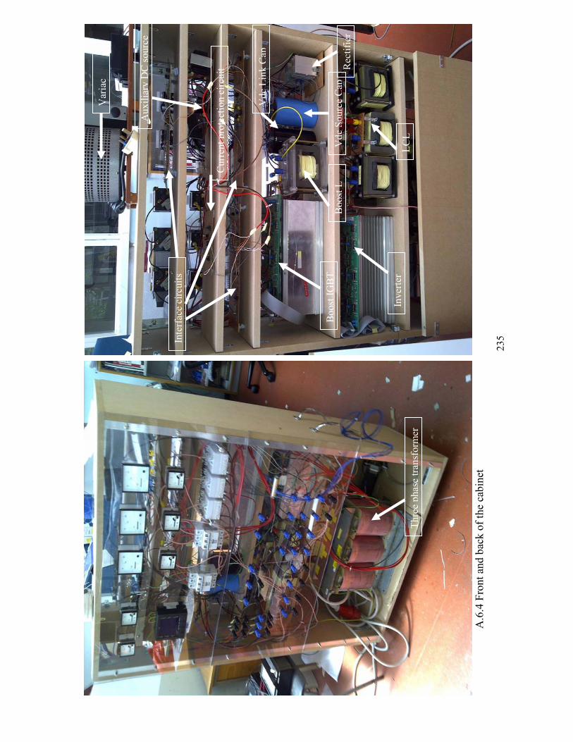
235
A.6
.4 F
ront
and b
ack o
f th
e ca
bin
et
Inver
ter
LC
L
Boost
IG
BT
Var
iac
Rec
tifi
er
Boost
L
Vdc
Sourc
e C
ap
Vdc
Lin
k C
ap
Inte
rfac
e ci
rcuit
s
Curr
ent
pro
tect
ion c
ircu
it
Auxil
iary
DC
sourc
e
Inver
ter
Thre
e phas
e tr
ansf
orm
er

236
A.6
.5 C
lose
vie
w o
f th
e ca
bin
et b
efore
mak
ings

237
Appendix 7: dSpace block set and Control Desk
A.7. 1: Screenshot of dSPace library and blocks
A.7. 2: DSP software: Control Desk

238
Appendix 8: List of publications
Conferences
M. Hanif, M. Basu and K. Gaughan,: “Novel AC side P&O Maximum Power
transfer control for Grid Connected Photovoltaic Systems”, International
Conference on Renewable Energies and Power Quality (ICREPQ), 2010 , 23th to 25th
March, 2010
M. Hanif,; U.D. Dwivedi,; M. Basu,; K. Gaughan,; , "Wavelet based islanding
detection of DC-AC inverter interfaced DG systems", Universities Power
Engineering Conference (UPEC), 2010 45th International , vol., no., pp.1-5, Aug. 31
2010-Sept. 3 2010
M. Hanif, M. Basu and K. Gaughan,: “A Discussion of Anti-islanding Protection
Schemes Incorporated in a Inverter Based DG”, International Conference on
Environment and Electrical Engineering (EEEIC) 2011, 10th
International, 8-11 May
2011

239
Journals
M. Hanif; M.Basu; K.Gaughan; , "Understanding the operation of a Z-source
inverter for photovoltaic application with a design example," Power Electronics,
IET , vol.4, no.3, pp.278-287, March 2011
M. Hanif, M. Basu, K. Gaughan “Wavelet Based Islanding Detection of Three-
Phase DC-AC Inverter Interfaced DG Systems”, ready to be submitted