is now part of - onsemi.com · an-9071–智能功率模块-spm™(采用 μmini dip spm...
TRANSCRIPT

To learn more about ON Semiconductor, please visit our website at www.onsemi.com
Is Now Part of
ON Semiconductor and the ON Semiconductor logo are trademarks of Semiconductor Components Industries, LLC dba ON Semiconductor or its subsidiaries in the United States and/or other countries. ON Semiconductor owns the rights to a number of patents, trademarks, copyrights, trade secrets, and other intellectual property. A listing of ON Semiconductor’s product/patent coverage may be accessed at www.onsemi.com/site/pdf/Patent-Marking.pdf. ON Semiconductor reserves the right to make changes without further notice to any products herein. ON Semiconductor makes no warranty, representation or guarantee regarding the suitability of its products for any particular purpose, nor does ON Semiconductor assume any liability arising out of the application or use of any product or circuit, and specifically disclaims any and all liability, including without limitation special, consequential or incidental damages. Buyer is responsible for its products and applications using ON Semiconductor products, including compliance with all laws, regulations and safety requirements or standards, regardless of any support or applications information provided by ON Semiconductor. “Typical” parameters which may be provided in ON Semiconductor data sheets and/or specifications can and do vary in different applications and actual performance may vary over time. All operating parameters, including “Typicals” must be validated for each customer application by customer’s technical experts. ON Semiconductor does not convey any license under its patent rights nor the rights of others. ON Semiconductor products are not designed, intended, or authorized for use as a critical component in life support systems or any FDA Class 3 medical devices or medical devices with a same or similar classification in a foreign jurisdiction or any devices intended for implantation in the human body. Should Buyer purchase or use ON Semiconductor products for any such unintended or unauthorized application, Buyer shall indemnify and hold ON Semiconductor and its officers, employees, subsidiaries, affiliates, and distributors harmless against all claims, costs, damages, and expenses, and reasonable attorney fees arising out of, directly or indirectly, any claim of personal injury or death associated with such unintended or unauthorized use, even if such claim alleges that ON Semiconductor was negligent regarding the design or manufacture of the part. ON Semiconductor is an Equal Opportunity/Affirmative Action Employer. This literature is subject to all applicable copyright laws and is not for resale in any manner.

www.fairchildsemi.com
© 2014 飞兆半导体公司 www.fairchildsemi.com
修订版 1.2 • 4/21/15
AN-9079
SPM® 2 系列热性能与安装扭矩
概述
对于半导体器件而言,最敏感的因素是结温。随着结温
升高,器件的工作特性也随之改变,故障率呈指数级上
升。这使得封装的热设计在器件的开发阶段以及应用
中,都成为一个十分重要的因素。尤其需注意,接触压
力或安装扭矩都可影响热性能。本应用指南揭示安装扭
矩和热阻之间的关系。
为了深入理解器件的热性能,通常要引入热阻概念。热
阻可定义为两个邻近等温面之间的温差与它们之间传递
总功率的比值。对于半导体器件而言,通常使用结温 TJ
和参考温度 Tx。功耗为器件工作时消耗的功率。参考点
的选取是任意的,但是通常会选择散热片所附器件背面
热量最集中的点。这个被称为结至壳热阻,RJC。当参
考点为周围环境温度时,就被称为结至环境热阻,
RJA。这两个参数都用于描述器件的热性能。RJC 通常
用于安装了散热片的器件,而 RJA 用于未安装散热片的
器件。图 1 显示了一个热网络,其中热量从 Motion
SPM 的结至环境处流出,包括散热片的热量。鉴于热阻
过大,虚线表示的器件 RCA 可以忽略。
TJ TC TH TA
RθJC RθHA
PD CJC CCH CHA
Transient impedanceof each section
RθCH
RθCA
Being ignored
图 1. 带散热片的瞬态热等效电路
Motion SPM 热阻定义为:
D
CJJC
P
TTR
(1)
式中,RJC (oC/W) 为结至壳体热阻和 PD (W)、TJ (
oC)
和 TC (°C) 分别为各器件的耗散功率、结温和壳体参考
温度。通过将 TC 替换为环境温度 (TA),可得到结至
环境热阻 RJA:
D
AJJA
P
TTR
(2)
其中,RJA 表示包括散热片在内的 SPM 整体热性能。
RJA 基本为热阻总 RJC、RCH 和 RHA 的总和:
HACHJCJA RRRR
(3)
其中,RCH 表示封装壳体和散热片之间的接触热阻,
空隙以导热硅膏填充,而 RHA 表示散热片的热阻。
从公式 (3) 可清楚看出,使 RJC、RCH 和 RHA 最小
化,对于最大化 SPM 的功率能力是至关重要的。假
设使用一个无限大的散热片,则可以认为 RCH 和
RHA 为零,且壳体温度 TC 锁定在恒定的环境温度
TA。通常,RCH 的值与导热硅膏的厚度成比例,并受
到装配工艺的限制。而通过选取适当的散热片,可微
调 RHA。
实际操作中,功耗 PD 并非一个恒定的直流值,而是一
个交流值。因此,应考虑图 1 中的瞬态 RC 等效电路。
对于脉冲功耗,热容效应会延缓结温的上升,因此允许
一个较大的 1200 V Motion SPM 2 系列负载。

AN-9079 应用指南
© 2013 飞兆半导体公司 www.fairchildsemi.com
修订版 1.2 • 4/21/15 2
图 2~图 7 显示 1200 V SPM2 系列的热阻曲线。热阻在
1 秒内进入饱和状态。其他类型的 Motion SPM 产品也
表现出相似的特性。
1E-6 1E-5 1E-4 1E-3 0.01 0.1 1 10 1000.0
0.2
0.4
0.6
0.8
1.0
1.2
1.4
1.6
1.8
2.0
Zth(J-C)_IGBT
Zth
(J-C
)
Pulse Duration [sec]
图 2. FNA21012A 的 IGBT 热阻抗曲线
1E-6 1E-5 1E-4 1E-3 0.01 0.1 1 10 1000.0
0.4
0.8
1.2
1.6
2.0
2.4
2.8
3.2
Zth(J-C)_FRD
Zth
(J-C
)
Pulse Duration [sec]
图 3. FNA21012A 的 FRD 热阻抗曲线
1E-6 1E-5 1E-4 1E-3 0.01 0.1 1 10 1000.0
0.1
0.2
0.3
0.4
0.5
0.6
0.7
0.8
0.9
1.0
Zth(J-C)_IGBT
Zth
(J-C
)
Pulse Duration [sec]
图 4. FNA22512A 的 IGBT 热阻抗曲线
1E-6 1E-5 1E-4 1E-3 0.01 0.1 1 10 1000.0
0.2
0.4
0.6
0.8
1.0
1.2
1.4
1.6
1.8
Zth(J-C)_FRD
Zth
(J-C
)
Pulse Duration [sec]
图 5. FNA22512A 的 FRD 热阻抗曲线
1E-6 1E-5 1E-4 1E-3 0.01 0.1 1 10 1000.0
0.1
0.2
0.3
0.4
0.5
0.6
0.7
0.8
0.9
Zth(J-C)_IGBT
Zth
(J-C
)
Pulse Duration [sec]
图 6. FNA23512A 的 IGBT 热阻抗曲线
1E-6 1E-5 1E-4 1E-3 0.01 0.1 1 10 1000.0
0.2
0.4
0.6
0.8
1.0
1.2
1.4
Zth(J-C)_FRD
Zth
(J-C
)
Pulse Duration [sec]
图 7. FNA23512A 的 FRD 热阻抗曲线
更多详情,请参考AN-9071,内容包括 SPM 45 系列搭
配各种类型散热片的热性能。
AN-9079 应用指南
© 2013 飞兆半导体公司 www.fairchildsemi.com
修订版 1.2 • 4/21/15 3
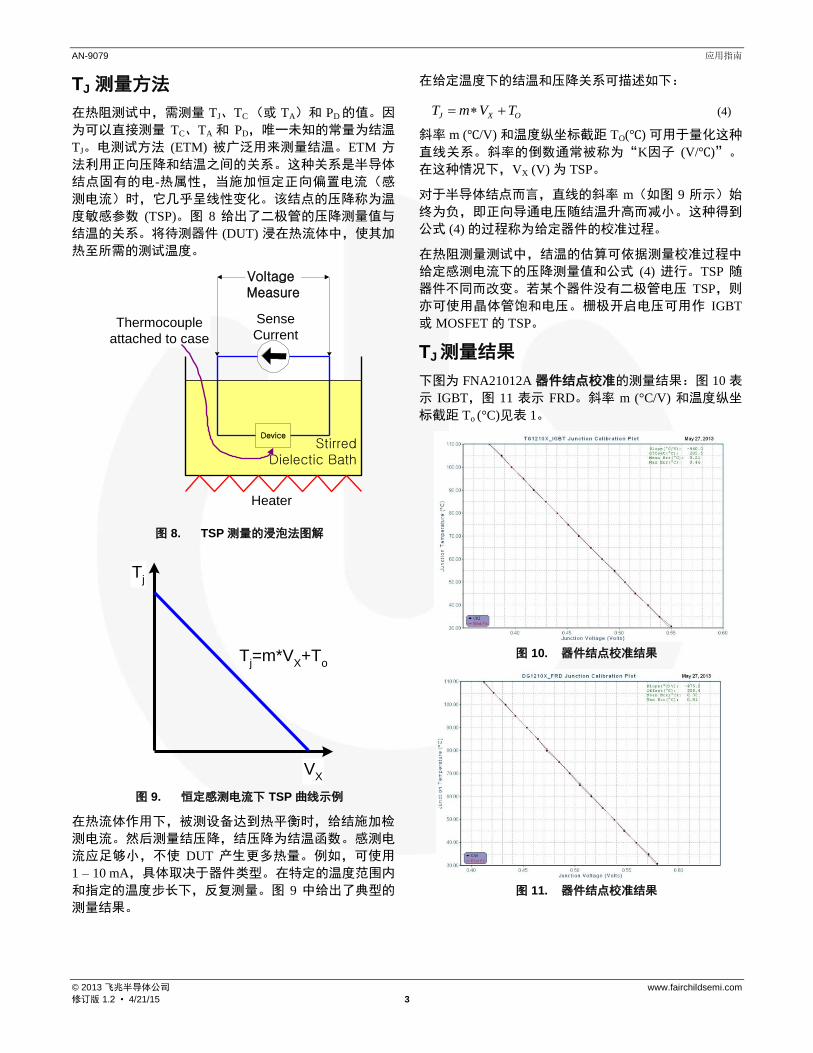
TJ 测量方法
在热阻测试中,需测量 TJ、TC (或 TA)和 PD 的值。因
为可以直接测量 TC、TA 和 PD,唯一未知的常量为结温
TJ。电测试方法 (ETM) 被广泛用来测量结温。ETM 方
法利用正向压降和结温之间的关系。这种关系是半导体
结点固有的电-热属性,当施加恒定正向偏置电流(感
测电流)时,它几乎呈线性变化。该结点的压降称为温
度敏感参数 (TSP)。图 8 给出了二极管的压降测量值与
结温的关系。将待测器件 (DUT) 浸在热流体中,使其加
热至所需的测试温度。
StirredDielectic Bath
Voltage Measure
Thermocouple
attached to case
Device
Heater
Sense
Current
图 8. TSP 测量的浸泡法图解
Tj=m*V
X+T
o
Tj
VX
图 9. 恒定感测电流下 TSP 曲线示例
在热流体作用下,被测设备达到热平衡时,给结施加检
测电流。然后测量结压降,结压降为结温函数。感测电
流应足够小,不使 DUT 产生更多热量。例如,可使用
1 – 10 mA,具体取决于器件类型。在特定的温度范围内
和指定的温度步长下,反复测量。图 9 中给出了典型的
测量结果。
在给定温度下的结温和压降关系可描述如下:
OXJ TVmT
(4)
斜率 m (℃/V) 和温度纵坐标截距 TO(℃) 可用于量化这种
直线关系。斜率的倒数通常被称为“K因子 (V/℃)”。
在这种情况下,VX (V) 为 TSP。
对于半导体结点而言,直线的斜率 m(如图 9 所示)始
终为负,即正向导通电压随结温升高而减小。这种得到
公式 (4) 的过程称为给定器件的校准过程。
在热阻测量测试中,结温的估算可依据测量校准过程中
给定感测电流下的压降测量值和公式 (4) 进行。TSP 随
器件不同而改变。若某个器件没有二极管电压 TSP,则
亦可使用晶体管饱和电压。栅极开启电压可用作 IGBT
或 MOSFET 的 TSP。
TJ 测量结果
下图为 FNA21012A 器件结点校准的测量结果:图 10 表
示 IGBT,图 11 表示 FRD。斜率 m (°C/V) 和温度纵坐
标截距 To (°C)见表 1。
图 10. 器件结点校准结果
图 11. 器件结点校准结果

AN-9079 应用指南
© 2013 飞兆半导体公司 www.fairchildsemi.com
修订版 1.2 • 4/21/15 4
表 1. FNA21012A 的 m (°C/V) 和温度纵坐标截距
To (V)
器件 m(°C/V) TO(°C) 感测电流
FNA21012A IGBT -460.0 282.5
10 mA FRD -475.2 305.3
热阻 RJC
结至外壳热阻 RJC 可通过公式 (1) 计算得到。通常热阻
在两个不同点测量——封装的中心点和芯片的中心点。
表 2 显示芯片中心点的测量值。
表 2. RJC: 热阻 °C/W
分类 SPL P(W) TJ TC RJC
FNA21012A
芯片中心
#1 62.28 121.10 60.40 0.97
#2 62.28 121.80 61.80 0.97
#3 62.28 120.50 60.10 0.96
SPM 产品数据表中的 RJC 采用芯片中心值,具有一定
的裕量,可适应制造商的某些不同要求。
热性能和安装扭矩的关系
功率器件对结温极为敏感。随着结温升高,器件的工作
特性也随之改变,故障率呈指数级上升。接触压力和安
装扭矩会影响热性能。
实际测量点
图 12 显示实际测量点,图 13 显示壳体温度的检测点
(数据表中的 TC 值)。
图 12. 实际测量点
图 13. 数据表规格中的壳体温度检测点
RJC_芯片中心于红点处进行测量,而 IGBT 在相同的红
点处直接受热。RJC_芯片中心不受封装翘曲和散热片翘
曲的影响,因为先接触该点,再接触器件的其余部分。
RJC_封装中心在红点处测量,而 IGBT 在黄点处受热。
AN-9079 应用指南
© 2013 飞兆半导体公司 www.fairchildsemi.com
修订版 1.2 • 4/21/15 5
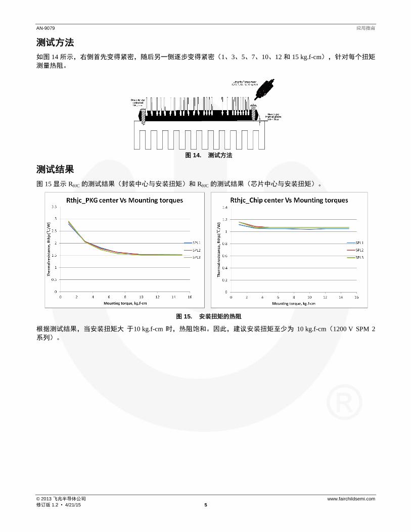
测试方法
如图 14 所示,右侧首先变得紧密,随后另一侧逐步变得紧密(1、3、5、7、10、12 和 15 kg.f-cm),针对每个扭矩
测量热阻。
图 14. 测试方法
测试结果
图 15 显示 RJC 的测试结果(封装中心与安装扭矩)和 RJC 的测试结果(芯片中心与安装扭矩)。
图 15. 安装扭矩的热阻
根据测试结果,当安装扭矩大 于10 kg.f-cm 时,热阻饱和。因此,建议安装扭矩至少为 10 kg.f-cm(1200 V SPM 2
系列)。

AN-9079 应用指南
© 2013 飞兆半导体公司 www.fairchildsemi.com
修订版 1.2 • 4/21/15 6
相关资源
AN-9071–智能功率模块-SPM™(采用 μMini DIP SPM 封装)热性能信息
AN-9075 – 1200V Motion SPM® 2 系列用户指南
AN-9076 – 新型 SPM® 2 封装安装指南
声明
飞兆半导体公司为提高产品的可靠性、功能或设计,保留对其作出变动的权利,恕不另行通知。对于本文描述的任何产品和电路在应用中所出现
的问题,飞兆半导体公司不承担任何责任;不转让其专利权下的任何许可证,也不转让其他权利。
生命支持政策
若无飞兆半导体公司总裁正式的书面授权,其产品不可作为生命支持设备或系统中的关键器件。
具体如下:
1. 生命支持器件或系统是指如下的设备或系统:(a)用于外科植入人体,或(b)支持或维持生命,以及(c)即使依照标示中的使用说明进行正确操
作,但若操作失败,仍将对使用者造成严重的伤害。
2. 关键器件是指生命支持设备或系统中,由于该器件的失效会导致整个生命支持设备或系统的失效,或是影响其安全性及使用效果。

www.onsemi.com1
ON Semiconductor and are trademarks of Semiconductor Components Industries, LLC dba ON Semiconductor or its subsidiaries in the United States and/or other countries.ON Semiconductor owns the rights to a number of patents, trademarks, copyrights, trade secrets, and other intellectual property. A listing of ON Semiconductor’s product/patentcoverage may be accessed at www.onsemi.com/site/pdf/Patent−Marking.pdf. ON Semiconductor reserves the right to make changes without further notice to any products herein.ON Semiconductor makes no warranty, representation or guarantee regarding the suitability of its products for any particular purpose, nor does ON Semiconductor assume any liabilityarising out of the application or use of any product or circuit, and specifically disclaims any and all liability, including without limitation special, consequential or incidental damages.Buyer is responsible for its products and applications using ON Semiconductor products, including compliance with all laws, regulations and safety requirements or standards,regardless of any support or applications information provided by ON Semiconductor. “Typical” parameters which may be provided in ON Semiconductor data sheets and/orspecifications can and do vary in different applications and actual performance may vary over time. All operating parameters, including “Typicals” must be validated for each customerapplication by customer’s technical experts. ON Semiconductor does not convey any license under its patent rights nor the rights of others. ON Semiconductor products are notdesigned, intended, or authorized for use as a critical component in life support systems or any FDA Class 3 medical devices or medical devices with a same or similar classificationin a foreign jurisdiction or any devices intended for implantation in the human body. Should Buyer purchase or use ON Semiconductor products for any such unintended or unauthorizedapplication, Buyer shall indemnify and hold ON Semiconductor and its officers, employees, subsidiaries, affiliates, and distributors harmless against all claims, costs, damages, andexpenses, and reasonable attorney fees arising out of, directly or indirectly, any claim of personal injury or death associated with such unintended or unauthorized use, even if suchclaim alleges that ON Semiconductor was negligent regarding the design or manufacture of the part. ON Semiconductor is an Equal Opportunity/Affirmative Action Employer. Thisliterature is subject to all applicable copyright laws and is not for resale in any manner.
PUBLICATION ORDERING INFORMATIONN. American Technical Support: 800−282−9855 Toll FreeUSA/Canada
Europe, Middle East and Africa Technical Support:Phone: 421 33 790 2910
Japan Customer Focus CenterPhone: 81−3−5817−1050
www.onsemi.com
LITERATURE FULFILLMENT:Literature Distribution Center for ON Semiconductor19521 E. 32nd Pkwy, Aurora, Colorado 80011 USAPhone: 303−675−2175 or 800−344−3860 Toll Free USA/CanadaFax: 303−675−2176 or 800−344−3867 Toll Free USA/CanadaEmail: [email protected]
ON Semiconductor Website: www.onsemi.com
Order Literature: http://www.onsemi.com/orderlit
For additional information, please contact your localSales Representative
© Semiconductor Components Industries, LLC