isl97678 datasheet - renesas.com
TRANSCRIPT
FN6998Rev.3.00
Sep 8, 2017
ISL976788-Channel 45V, 50mA LED Driver
DATASHEET
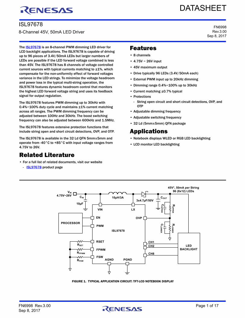
The ISL97678 is an 8-channel PWM dimming LED driver for LCD backlight applications. The ISL97678 is capable of driving up to 96 pieces of 3.4V/50mA LEDs but larger numbers of LEDs are possible if the LED forward voltage combined is less than 45V. The ISL97678 has 8 channels of voltage controlled current sources with typical currents matching to ±1%, which compensate for the non-uniformity effect of forward voltages variance in the LED strings. To minimize the voltage headroom and power loss in the typical multi-string operation, the ISL97678 features dynamic headroom control that monitors the highest LED forward voltage string and uses its feedback signal for output regulation.
The ISL97678 features PWM dimming up to 30kHz with 0.4%~100% duty cycle and maintains ±1% current matching across all ranges. The PWM dimming frequency can be adjusted between 100Hz and 30kHz. The boost switching frequency can also be adjusted between 600kHz and 1.5MHz.
The ISL97678 features extensive protection functions that include string open and short circuit detections, OVP, and OTP.
The ISL97678 is available in the 32 Ld QFN 5mmx5mm and operate from -40°C to +85°C with input voltage ranges from 4.75V to 26V.
Related Literature• For a full list of related documents, visit our website
- ISL97678 product page
Features• 8 channels
• 4.75V ~ 26V input
• 45V maximum output
• Drive typically 96 LEDs (3.4V/50mA each)
• External PWM input up to 20kHz dimming
• Dimming range 0.4%~100% up to 30kHz
• Current matching ±0.7% typical
• Protections
- String open circuit and short circuit detections, OVP, and OTP
• Adjustable dimming frequency
• Adjustable switching frequency
• 32 Ld (5mmx5mm) QFN package
Applications• Notebook displays WLED or RGB LED backlighting
• LCD monitor LED backlighting
FIGURE 1. TYPICAL APPLICATION CIRCUIT: TFT-LCD NOTEBOOK DISPLAY
VIN
CH1RSET
LEDBACKLIGHT
PROCESSOR
OVP
FSW
45V*, 50mA per String96 (8x12) LEDs
LX
VIN
4.75V~26V
FPWM
EN
PGND
CH2
CH8
PWM
AGND
3x4.7µF/50V10µF R
UP
PE
RR
LO
WE
R
CU
PP
ER
CL
OW
ER
RSET
RFPWM
RFSW
COUTCIN 10µH/3A
ISL97678
FN6998 Rev.3.00 Page 1 of 17Sep 8, 2017
ISL97678
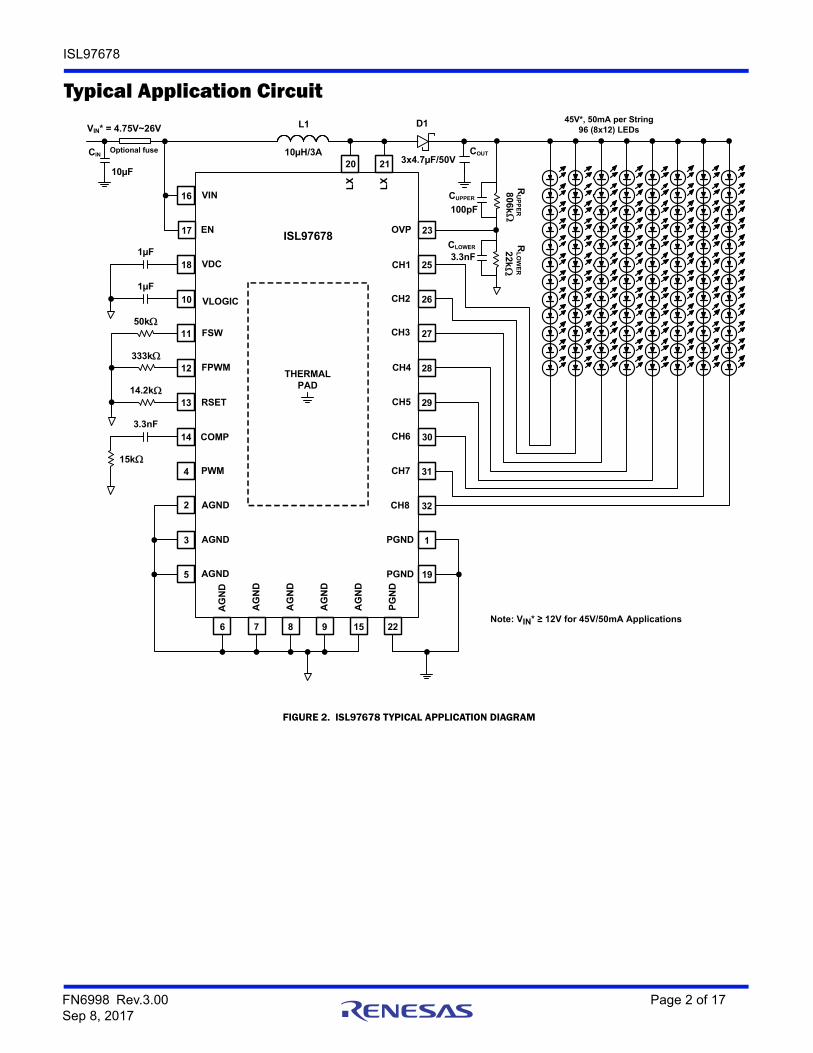
Typical Application Circuit
FIGURE 2. ISL97678 TYPICAL APPLICATION DIAGRAM
VIN
COMP
RSET
FSW
VDC
45V*, 50mA per String96 (8x12) LEDs
L1VIN* = 4.75V~26V
FPWM
Optional fuse
ENISL97678
PWM
VLOGIC
AGND
RU
PP
ER
RL
OW
ER
3x4.7µF/50V
4
LX
LX
20 2110µH/3A
14
10
18
17
16
11
12
13
AG
ND
AG
ND
AG
ND
AG
ND
AG
ND
PG
ND
AGND
5
6 7 8 159
OVP
D1
23
COUT
PGND
PGNDAGND
2
3
22
19
1
CH1
CH2
CH3
CH4
CH5
CH6
CH7
CH8
25
26
27
28
29
30
31
32
THERMAL PAD
CIN
10µF
1µF
1µF
50k
333k
14.2k
3.3nF
15k
806k
22k
100pF
3.3nF
CUPPER
CLOWER
Note: VIN* ≥ 12V for 45V/50mA Applications
FN6998 Rev.3.00 Page 2 of 17Sep 8, 2017
ISL97678
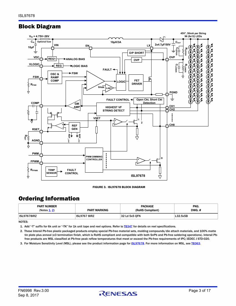
Block Diagram
FIGURE 3. ISL97678 BLOCK DIAGRAM
REFGEN
VIN
GMAMP
COMPCH1
LOGIC FETDRIVER
OVPREG1
OSC & RAMP COMP
Imax ILIMIT
HIGHEST VF STRING DETECT
RSET
O/P SHORT
RE
F_
OV
P
RE
F_
VS
C
ANALOG BIAS
Open Ckt, Short CktDetection
1
OVP
FSW
VDC
PWM DIMMING CONTROLLER
2
45V*, 50mA per String96 (8x12) LEDs
LX
VIN = 4.75V~26V
FPWM
EN
PGND
ISL97678
CH2
CH8
PWM
+-
+-
8+-
REG LOGIC BIASVLOGIC
FSWFAULT
AGND
VSET
TEMPSENSOR
FAULT CONTROL
2x4.7µF/50V
FAULT CONTROL
10µH/3AOptional fuse
10µF RU
PP
ER
RL
OW
ER
CU
PP
ER
CL
OW
ER
RS
ET
RFPWM
RFSW
COUTCIN
Ordering InformationPART NUMBER
(Notes 1, 2) PART MARKINGPACKAGE
(RoHS Compliant)PKG.
DWG. #
ISL97678IRZ ISL9767 8IRZ 32 Ld 5x5 QFN L32.5x5B
NOTES:
1. Add “-T” suffix for 6k unit or “-TK” for 1k unit tape and reel options. Refer to TB347 for details on reel specifications.
2. These Intersil Pb-free plastic packaged products employ special Pb-free material sets, molding compounds/die attach materials, and 100% matte tin plate plus anneal (e3 termination finish, which is RoHS compliant and compatible with both SnPb and Pb-free soldering operations). Intersil Pb-free products are MSL classified at Pb-free peak reflow temperatures that meet or exceed the Pb-free requirements of IPC/JEDEC J STD-020.
3. For Moisture Sensitivity Level (MSL), please see the product information page for ISL97678. For more information on MSL, see TB363.
FN6998 Rev.3.00 Page 3 of 17Sep 8, 2017
ISL97678
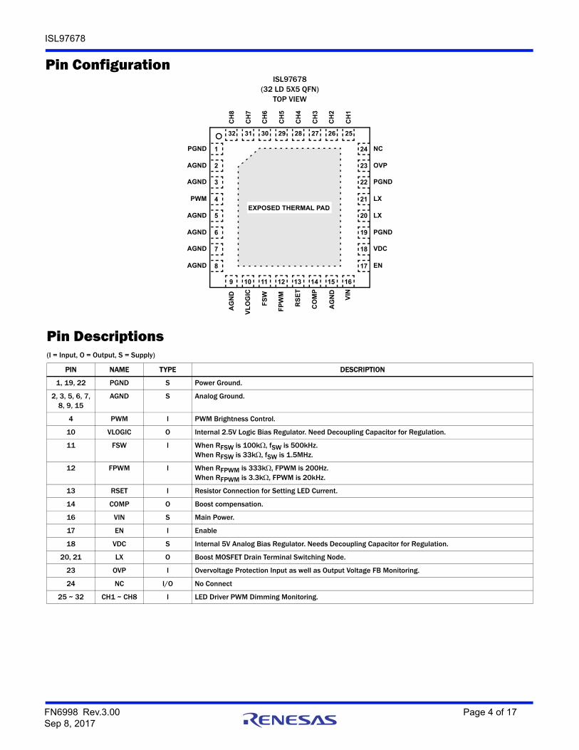
Pin ConfigurationISL97678
(32 LD 5X5 QFN)TOP VIEW
CH
8
CH
7
CH
6
CH
5
CH
4
CH
3
CH
2
CH
1
AG
ND
VL
OG
IC
FS
W
FP
WM
RS
ET
CO
MP
AG
ND
VIN
PGND
AGND
AGND
PWM
AGND
AGND
AGND
AGND
NC
OVP
PGND
LX
LX
PGND
VDC
EN
1
2
3
4
5
6
7
8
24
23
22
21
20
19
18
17
32 31 30 29 28 27 26 25
9 10 11 12 13 14 15 16
EXPOSED THERMAL PAD
Pin Descriptions(I = Input, O = Output, S = Supply)
PIN NAME TYPE DESCRIPTION
1, 19, 22 PGND S Power Ground.
2, 3, 5, 6, 7, 8, 9, 15
AGND S Analog Ground.
4 PWM I PWM Brightness Control.
10 VLOGIC O Internal 2.5V Logic Bias Regulator. Need Decoupling Capacitor for Regulation.
11 FSW I When RFSW is 100k, fSW is 500kHz.When RFSW is 33k, fSW is 1.5MHz.
12 FPWM I When RFPWM is 333k, FPWM is 200Hz.When RFPWM is 3.3k, FPWM is 20kHz.
13 RSET I Resistor Connection for Setting LED Current.
14 COMP O Boost compensation.
16 VIN S Main Power.
17 EN I Enable
18 VDC S Internal 5V Analog Bias Regulator. Needs Decoupling Capacitor for Regulation.
20, 21 LX O Boost MOSFET Drain Terminal Switching Node.
23 OVP I Overvoltage Protection Input as well as Output Voltage FB Monitoring.
24 NC I/O No Connect
25 ~ 32 CH1 ~ CH8 I LED Driver PWM Dimming Monitoring.
FN6998 Rev.3.00 Page 4 of 17Sep 8, 2017
ISL97678
5.
Absolute Maximum Ratings Thermal InformationVoltage ratings are all with respect to AGND pinVIN . . . . . . . . . . . . . . . . . . . . . . . . . . . . . . . . . . . . . . . . . . . . . . . . . -0.3V to 27VEN . . . . . . . . . . . . . . . . . . . . . . . . . . . . . . . . . . . . . . . . . . . . . . . . . . -0.3V to 27VVLOGIC . . . . . . . . . . . . . . . . . . . . . . . . . . . . . . . . . . . . . . . . . . . . -0.3V to 2.75VVDC, PWM . . . . . . . . . . . . . . . . . . . . . . . . . . . . . . . . . . . . . . . . . -0.3V to 5.75VCOMP, RSET, FPWM, FSW . . . . . . . . . . . . . . . . . . . . . . . . . . . . . -0.3V to min . . . . . . . . . . . . . . . . . . . . . . . . . . . . . . . . . . . . . . . . . . . . . .(VDC + 0.3V, 5.75V)CH1 - CH8, LX, OVP. . . . . . . . . . . . . . . . . . . . . . . . . . . . . . . . . . . . -0.3V to 45VPGND, AGND . . . . . . . . . . . . . . . . . . . . . . . . . . . . . . . . . . . . . . . -0.3V to +0.3V
Recommended Operating ConditionsTemperature Range . . . . . . . . . . . . . . . . . . . . . . . . . . . . . . . . -40°C to +85°C
Thermal Resistance (Typical) JA (°C/W) JC (°C/W)32 Ld QFN (Notes 4, 5). . . . . . . . . . . . . . . . . 31 3
Thermal Characterization (Typical, Note 6) PSIJT (°C/W)
32 Ld QFN . . . . . . . . . . . . . . . . . . . . . . . . . . . . . . . . . . . . . 0.2Maximum Continuous Junction Temperature . . . . . . . . . . . . . . . . .+125°CStorage Temperature . . . . . . . . . . . . . . . . . . . . . . . . . . . . .-65°C to +150°CPower DissipationTA < +25°C . . . . . . . . . . . . . . . . . . . . . . . . . . . . . . . . . . . . . . . . . . . . . . . . 3.2WTA < +70°C . . . . . . . . . . . . . . . . . . . . . . . . . . . . . . . . . . . . . . . . . . . . . . . . 1.8WTA < +85°C . . . . . . . . . . . . . . . . . . . . . . . . . . . . . . . . . . . . . . . . . . . . . . . . 1.3WTA < +100°C . . . . . . . . . . . . . . . . . . . . . . . . . . . . . . . . . . . . . . . . . . . . . . 0.8WPb-Free Reflow Profile . . . . . . . . . . . . . . . . . . . . . . . . . . . . . . . . . . see TB493
CAUTION: Do not operate at or near the maximum ratings listed for extended periods of time. Exposure to such conditions may adversely impact productreliability and result in failures not covered by warranty.
NOTES:
4. JA is measured with the component mounted on a high-effective thermal conductivity test board in free air. See TB379 for details.
5. For JC, the “case temp” location is the center of the exposed metal pad on the package underside.
6. PSIJT is the PSI junction-to-top thermal characterization parameter. If the package top temperature can be measured with this rating then the die junction temperature can be estimated more accurately than the JA and JC thermal resistance ratings.
Electrical Specifications All specifications below are characterized at TA = -40°C to +85°C; VIN = 12V, EN = 5V, RSET = 36kΩ, unless otherwise noted. Boldface limits apply over the operating temperature range, -40°C to +85°C.
PARAMETER DESCRIPTION TEST CONDITIONSMIN
(Note 7) TYPMAX
(Note 7) UNITS
GENERAL
VIN Backlight Supply Voltage 4.75 26 (Note 8)
V
IVIN_SHDN VIN Shutdown Current EN = 0 5 µA
VOUT Output Voltage 45 V
VUVLO Undervoltage Lockout Threshold 2.9 3.3 V
VUVLO_HYS Undervoltage Lockout Hysteresis 300 mV
LINEAR REGULATOR
VDC 5V Analog Bias Regulator VIN > 6V 4.8 5 5.1 V
VDC_DROP VDC LDO Dropout Voltage IVDC = 30mA 71 100 mV
IVDC Active Current EN = 5V, R = 33kΩ 10 mA
VLOGIC 2.5V Logic Bias Regulator VIN > 6V 2.3 2.4 2.5 V
VLOGIC_DROP VLOGIC LDO Dropout Voltage IVLOGIC = 30mA 31 100 mV
BOOST SWITCHING REGULATOR
SS Soft-Start 16 ms
SWILimit Boost FET Current Limit TA = +25°C to +85°C 3.0 4.7 A
rDS(ON) Internal Boost Switch ON-Resistance 130 mΩ
VFSW fSW Voltage RFSW = 33kΩ 1.18 1.21 1.24 V
FN6998 Rev.3.00 Page 5 of 17Sep 8, 2017
ISL97678
Eff_peak Peak Efficiency VIN = 24V, 96LEDs, 20mA each, L = 10µH with DCR 100mΩFSW = 600kHz, TA = +25°C
92.4 %
VIN = 12V, 96 LEDs, 20mA each, L = 10µH with DCR 100mΩFSW = 600kHz, TA = +25°C
91.5 %
VIN = 6V, 96 LEDs, 20mA each, L = 10µH with DCR 100mΩFSW = 600kHz, TA = +25°C
81.6 %
VIN = 24V, 80 LEDs, 40mA each, L = 10µH with DCR 100mΩFSW=600kHz, TA = +25°C
93.4 %
VIN = 12V, 80 LEDs, 40mA each, L = 10µH with DCR 100mΩFSW = 600kHz, TA = +25°C
90.7 %
DMAX Boost Maximum Duty Cycle fSW = 500kHz 90 %
DMIN Boost Minimum Duty Cycle fSW = 500kHz 10 %
fSW Boost Switching Frequency RFSW = 100kΩ 0.45 0.5 0.55 MHz
RFSW = 33kΩ 1.35 1.5 1.65 MHz
ILX_leakage Lx Leakage Current VLX = 45V, EN= 0V 10 µA
REFERENCE
IMATCH Channel-to-Channel Current Matching ILED = 20mA -1.1 ±0.7 +1.1 %
IACC Absolute Current Accuracy RSET = 36kΩTA = +25°C -1.5 +1.5 %
RSET = 36kΩTA = -40°C to +80°C
-2 +2 %
FAULT DETECTION
VSC Channel Short Circuit Threshold 3.3 4.6 V
Vtemp Over-Temperature Threshold 150 °C
Vtemp_acc Over-Temperature Threshold Accuracy 5 °C
VOVP Overvoltage Limit on OVP Pin 1.18 1.22 1.24 V
DIGITAL INTERFACE
VIL Logic Input Low Voltage 0.8 V
VIH Logic Input High Voltage 1.5 5.5 V
CURRENT SOURCES
VHEADROOM Dominant Channel Current Source Headroom at CH Pin
ILED = 50mATA = +25°C
1.0(Note 10)
V
VHEADROOM_RANGE Dominant Channel Current Sink Headroom Range at CHx Pin
ILED = 50mATA = +25°C
90 mV
VRSET Voltage at RSET Pin 1.18 1.21 1.24 V
Electrical Specifications All specifications below are characterized at TA = -40°C to +85°C; VIN = 12V, EN = 5V, RSET = 36kΩ, unless otherwise noted. Boldface limits apply over the operating temperature range, -40°C to +85°C. (Continued)
PARAMETER DESCRIPTION TEST CONDITIONSMIN
(Note 7) TYPMAX
(Note 7) UNITS
FN6998 Rev.3.00 Page 6 of 17Sep 8, 2017
ISL97678
ILEDmax Maximum LED Current per Channel LED config = 8P10S with VF = 3.4V and VIN = 11V
50 mA
PWM GENERATOR
FPWM Generated PWM Frequency RFPWM = 330kΩ 180 200 220 Hz
RFPWM = 3.3kΩ 18 20 22 kHz
Dimming Range PWM Dimming Duty Cycle Limits (Note 9) fPWM 30kHz 0.4 100 %
FPWMI PWMI Input Frequency Range (Note 9) 200 20k Hz
VFPWM VFPWM Voltage RFPWM = 3.3kΩ 1.18 1.21 1.25 V
NOTES:
7. Parameters with MIN and/or MAX limits are 100% tested at +25°C, unless otherwise specified. Temperature limits established by characterization and are not production tested.
8. At maximum VIN of 26V, minimum VOUT is 28V. Minimum VOUT can be lower at lower VIN9. Limits established by characterization and are not production tested.
10. Varies within range specified by VHEADROOM_RANGE.
Electrical Specifications All specifications below are characterized at TA = -40°C to +85°C; VIN = 12V, EN = 5V, RSET = 36kΩ, unless otherwise noted. Boldface limits apply over the operating temperature range, -40°C to +85°C. (Continued)
PARAMETER DESCRIPTION TEST CONDITIONSMIN
(Note 7) TYPMAX
(Note 7) UNITS
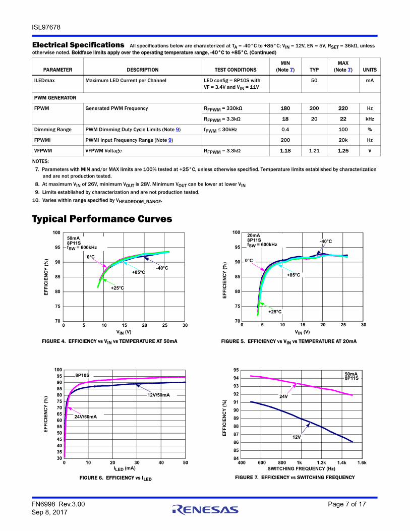
Typical Performance Curves
FIGURE 4. EFFICIENCY vs VIN vs TEMPERATURE AT 50mA FIGURE 5. EFFICIENCY vs VIN vs TEMPERATURE AT 20mA
FIGURE 6. EFFICIENCY vs ILED FIGURE 7. EFFICIENCY vs SWITCHING FREQUENCY
70
75
80
85
90
95
100
0 5 10 15 20 25 30
VIN (V)
EF
FIC
IEN
CY
(%
)
50mA8P11SfSW = 600kHz
0°C
+25°C
+85°C-40°C
70
75
80
85
90
95
100
0 5 10 15 20 25 30
VIN (V)
EF
FIC
IEN
CY
(%
)
20mA8P11SfSW = 600kHz
0°C
+25°C
+85°C
-40°C
3035404550556065707580859095
100
0 10 20 30 40 50ILED (mA)
EF
FIC
IEN
CY
(%
)
8P10S
24V/50mA
12V/50mA
84
85
86
87
88
89
90
91
92
93
94
95
400 600 800 1k 1.2k 1.4k 1.6kSWITCHING FREQUENCY (Hz)
EF
FIC
IEN
CY
(%
)
50mA 8P11S
24V
12V
FN6998 Rev.3.00 Page 7 of 17Sep 8, 2017
ISL97678
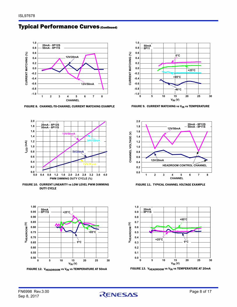
FIGURE 8. CHANNEL-TO-CHANNEL CURRENT MATCHING EXAMPLE FIGURE 9. CURRENT MATCHING vs VIN vs TEMPERATURE
FIGURE 10. CURRENT LINEARITY vs LOW LEVEL PWM DIMMING DUTY CYCLE
FIGURE 11. TYPICAL CHANNEL VOLTAGE EXAMPLE
FIGURE 12. VHEADROOM vs VIN vs TEMPERATURE AT 50mA FIGURE 13. VHEADROOM vs VIN vs TEMPERATURE AT 20mA
Typical Performance Curves (Continued)
-1.0
-0.8
-0.6
-0.4
-0.2
0.0
0.2
0.4
0.6
0.8
1.0
1 3 6
CHANNEL
CU
RR
EN
T M
AT
CH
ING
(%
)
20mA - 8P12S50mA - 8P11S
2 4 5 7 8
12V/50mA
12V/20mA
-1.0
-0.8
-0.6
-0.4
-0.2
0.0
0.2
0.4
0.6
0.8
1.0
0 5 10 15 20 25 30VIN (V)
CU
RR
EN
T M
AT
CH
ING
(%
)
50mA8P11
0°C
-40°C
+85°C
+25°C
0.0
0.2
0.4
0.6
0.8
1.0
1.2
1.4
1.6
1.8
2.0
0.0 0.4 0.8 1.2 1.6 2.0 2.4 2.8 3.2 3.6 4.0
PWM DIMMING DUTY CYCLE (%)
I LE
D (
mA
)
20mA - 8P12S50mA - 8P11S
12V/50mA
5V/20mA
24V/20mA
24V/50mA
0.0
0.2
0.4
0.6
0.8
1.0
1.2
1.4
1.6
1.8
2.0
1 2 3 5 7 8CHANNEL
CH
AN
NE
L V
OLT
AG
E (
V)
20mA - 8P12S50mA - 8P11S
4 6
12V/50mA
12V/20mA
HEADROOM CONTROL CHANNEL
0.50
0.55
0.60
0.65
0.70
0.75
0.80
0.85
0.90
0.95
1.00
0 5 10 15 20 25 30VIN (V)
VH
EA
DR
OO
M (
V)
50mA8P11S +25°C
+85°C
0°C
0.0
0.1
0.2
0.3
0.4
0.5
0.6
0.7
0.8
0.9
1.0
0 5 10 15 20 25 30VIN (V)
VH
EA
DR
OO
M (
V)
20mA8P11S
+25°C
+85°C
0°C
FN6998 Rev.3.00 Page 8 of 17Sep 8, 2017
ISL97678
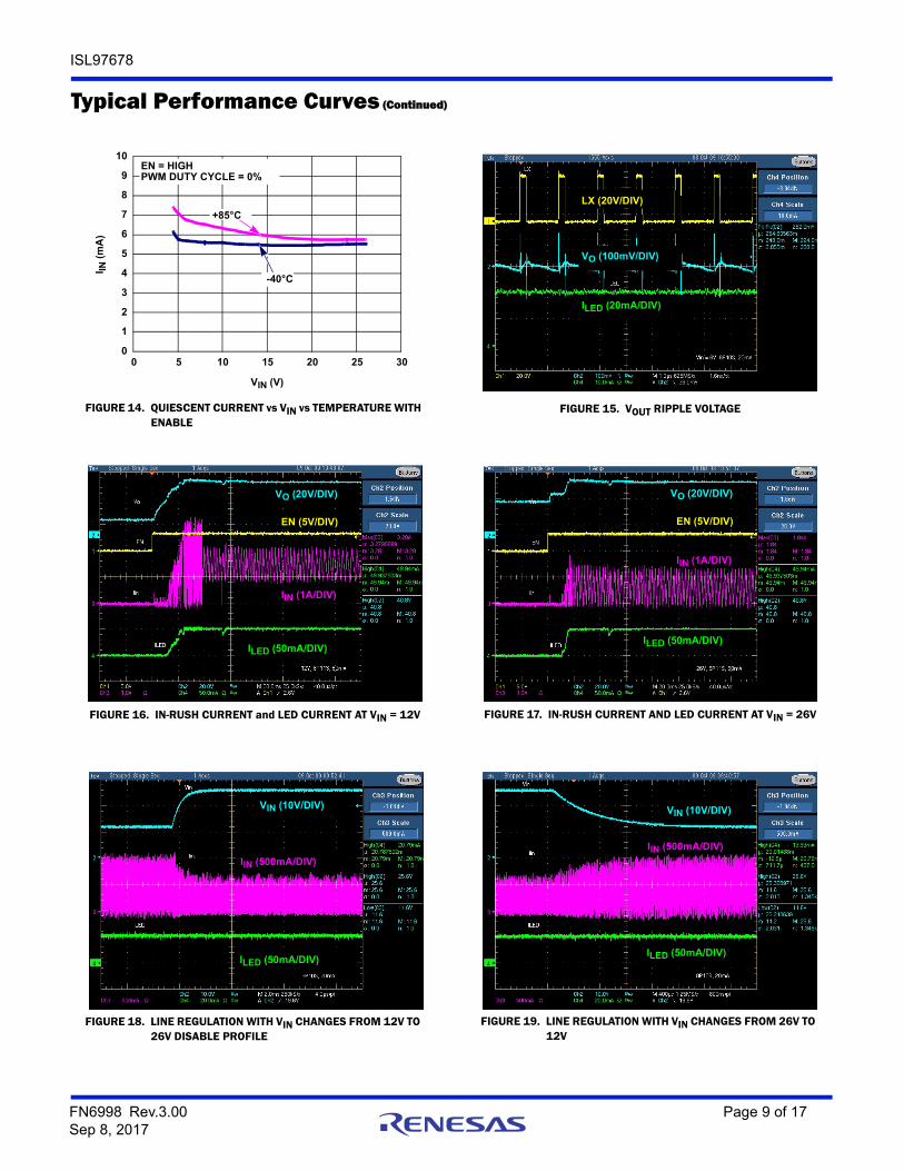
FIGURE 14. QUIESCENT CURRENT vs VIN vs TEMPERATURE WITH ENABLE
FIGURE 15. VOUT RIPPLE VOLTAGE
FIGURE 16. IN-RUSH CURRENT and LED CURRENT AT VIN = 12V FIGURE 17. IN-RUSH CURRENT AND LED CURRENT AT VIN = 26V
FIGURE 18. LINE REGULATION WITH VIN CHANGES FROM 12V TO 26V DISABLE PROFILE
FIGURE 19. LINE REGULATION WITH VIN CHANGES FROM 26V TO 12V
Typical Performance Curves (Continued)
0
1
2
3
4
5
6
7
8
9
10
0 5 10 15 20 25 30
VIN (V)
I IN (
mA
)
EN = HIGHPWM DUTY CYCLE = 0%
+85°C
-40°C
LX (20V/DIV)
VO (100mV/DIV)
ILED (20mA/DIV)
EN (5V/DIV)
VO (20V/DIV)
ILED (50mA/DIV)
IIN (1A/DIV)
EN (5V/DIV)
VO (20V/DIV)
ILED (50mA/DIV)
IIN (1A/DIV)
VIN (10V/DIV)
ILED (50mA/DIV)
IIN (500mA/DIV)
VIN (10V/DIV)
ILED (50mA/DIV)
IIN (500mA/DIV)
FN6998 Rev.3.00 Page 9 of 17Sep 8, 2017
ISL97678
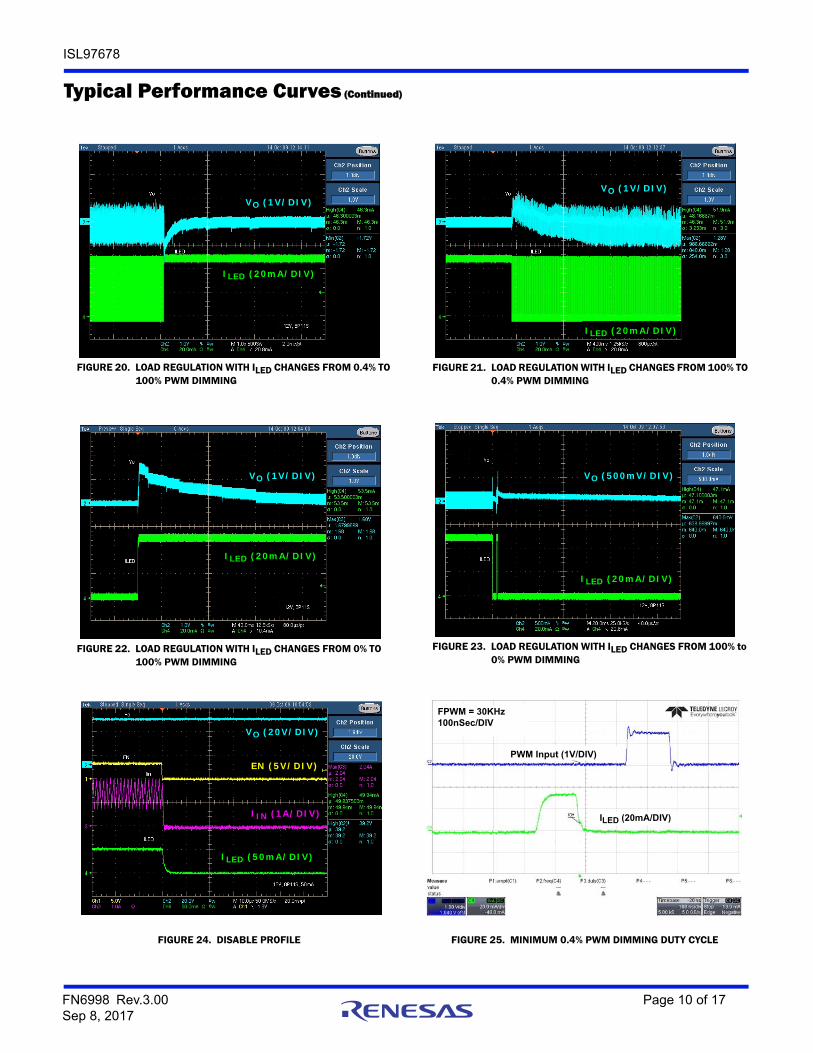
FIGURE 20. LOAD REGULATION WITH ILED CHANGES FROM 0.4% TO 100% PWM DIMMING
FIGURE 21. LOAD REGULATION WITH ILED CHANGES FROM 100% TO 0.4% PWM DIMMING
FIGURE 22. LOAD REGULATION WITH ILED CHANGES FROM 0% TO 100% PWM DIMMING
FIGURE 23. LOAD REGULATION WITH ILED CHANGES FROM 100% to 0% PWM DIMMING
FIGURE 24. DISABLE PROFILE FIGURE 25. MINIMUM 0.4% PWM DIMMING DUTY CYCLE
Typical Performance Curves (Continued)
VO (1V/DIV)
ILED (20mA/DIV)
VO (1V/DIV)
ILED (20mA/DIV)
VO (1V/DIV)
ILED (20mA/DIV)
VO (500mV/DIV)
ILED (20mA/DIV)
EN (5V/DIV)
VO (20V/DIV)
ILED (50mA/DIV)
IIN (1A/DIV)
FPWM = 30KHz100nSec/DIV
ILED (20mA/DIV)
PWM Input (1V/DIV)
FN6998 Rev.3.00 Page 10 of 17Sep 8, 2017
ISL97678
Theory of OperationPWM Boost ConverterThe current mode PWM boost converter produces the minimal voltage needed to enable the LED string with the highest forward voltage drop to run at the programmed current. The ISL97678 employs current mode control boost architecture, which has a fast current sense loop and a slow voltage feedback loop. This architecture achieves a fast transient response that is essential for notebook backlight applications in which the power can be several Li-ion cell batteries that instantly change to an AC/DC adapter without rendering a noticeable visual nuisance. The number of LEDs that can be driven by the ISL97678 depends on the type of LED chosen in the application. The ISL97678 is capable of boosting up to 45V and drive eight channels of LEDs at a maximum of 45mA per channel.
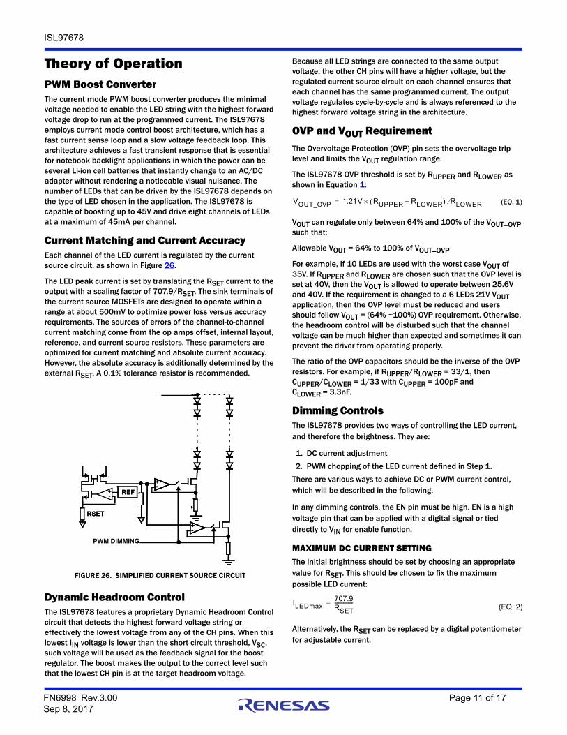
Current Matching and Current AccuracyEach channel of the LED current is regulated by the current source circuit, as shown in Figure 26.
The LED peak current is set by translating the RSET current to the output with a scaling factor of 707.9/RSET. The sink terminals of the current source MOSFETs are designed to operate within a range at about 500mV to optimize power loss versus accuracy requirements. The sources of errors of the channel-to-channel current matching come from the op amps offset, internal layout, reference, and current source resistors. These parameters are optimized for current matching and absolute current accuracy. However, the absolute accuracy is additionally determined by the external RSET. A 0.1% tolerance resistor is recommended..
Dynamic Headroom ControlThe ISL97678 features a proprietary Dynamic Headroom Control circuit that detects the highest forward voltage string or effectively the lowest voltage from any of the CH pins. When this lowest IIN voltage is lower than the short circuit threshold, VSC, such voltage will be used as the feedback signal for the boost regulator. The boost makes the output to the correct level such that the lowest CH pin is at the target headroom voltage.
Because all LED strings are connected to the same output voltage, the other CH pins will have a higher voltage, but the regulated current source circuit on each channel ensures that each channel has the same programmed current. The output voltage regulates cycle-by-cycle and is always referenced to the highest forward voltage string in the architecture.
OVP and VOUT Requirement
The Overvoltage Protection (OVP) pin sets the overvoltage trip level and limits the VOUT regulation range.
The ISL97678 OVP threshold is set by RUPPER and RLOWER as shown in Equation 1:
VOUT can regulate only between 64% and 100% of the VOUT_OVP such that:
Allowable VOUT = 64% to 100% of VOUT_OVP
For example, if 10 LEDs are used with the worst case VOUT of 35V. If RUPPER and RLOWER are chosen such that the OVP level is set at 40V, then the VOUT is allowed to operate between 25.6V and 40V. If the requirement is changed to a 6 LEDs 21V VOUT application, then the OVP level must be reduced and users should follow VOUT = (64% ~100%) OVP requirement. Otherwise, the headroom control will be disturbed such that the channel voltage can be much higher than expected and sometimes it can prevent the driver from operating properly.
The ratio of the OVP capacitors should be the inverse of the OVP resistors. For example, if RUPPER/RLOWER = 33/1, then CUPPER/CLOWER = 1/33 with CUPPER = 100pF and CLOWER = 3.3nF.
Dimming ControlsThe ISL97678 provides two ways of controlling the LED current, and therefore the brightness. They are:
1. DC current adjustment
2. PWM chopping of the LED current defined in Step 1.
There are various ways to achieve DC or PWM current control, which will be described in the following.
In any dimming controls, the EN pin must be high. EN is a high voltage pin that can be applied with a digital signal or tied directly to VIN for enable function.
MAXIMUM DC CURRENT SETTINGThe initial brightness should be set by choosing an appropriate value for RSET. This should be chosen to fix the maximum possible LED current:
Alternatively, the RSET can be replaced by a digital potentiometer for adjustable current.
FIGURE 26. SIMPLIFIED CURRENT SOURCE CIRCUIT
REF
+-
+-
PWM DIMMING
RSET
+ REF-
+-
RSET
-
VOUT_OVP 1.21V RUPPER RLOWER+ RLOWER= (EQ. 1)
ILEDmax707.9RSET---------------= (EQ. 2)
FN6998 Rev.3.00 Page 11 of 17Sep 8, 2017

ISL97678
PWM CONTROLThe ISL97678 provides PWM dimming by PWM chopping of the current in the LEDs for all eight channels. To achieve PWM dimming, the user must apply a PWM signal at the PWM pin. The PWM output follows the PWM input and the dimming frequency is set by RPWM. During the On periods, the LED current is defined by the value of RSET, as described in Equation 1.
PWM Dimming Frequency AdjustmentThe dimming frequencies are set by an external resistor at the FPWM pin as shown by Equation 3:
where fPWM is the desirable PWM dimming frequency and RFPWM is the setting resistor. fPWM range is from 100Hz to 30kHz.
Switching FrequencyThe boost switching frequency can be adjusted by a resistor as shown in Equation 4:
where fSW is the desirable boost switching frequency and RFSW is the setting resistor.
5V and 2.3V Low Dropout RegulatorsA 5V LDO regulator is present at the VDC pin to develop the necessary low voltage supply, which is used by the chips internal control circuitry. Because VDC is an LDO pin, it requires a bypass capacitor of 1µF or more for the regulation. The VDC pin can be used for a coarse regulator or reference but does not pull more than a few mA from it.
Similarly, a 2.3V LDO regulator is present at the VLOGIC pin to develop the necessary low voltage supply for the chip’s internal logic control circuitry. A 1µF bypass capacitor or more is needed for regulation. The VLOGIC pin can be used as a coarse regulator or reference but does not pull more than a few mA from it.
Soft-Start The ISL97678 uses a digital soft-start in which the boost current limit is stepped up in eight steps. The initial current limit level is set to one ninth of the full current limit, with subsequent steps increasing this by a ninth every 2ms. If no LEDs are conducting during the interval since the last step (for example, if the LEDs are running at a low duty cycle at a low PWM frequency) then the step will be delayed until the LEDs are conducting. If the LEDs are disabled and re-enabled again then soft-start will be restarted when the LEDs are enabled.
Fault Protection and MonitoringThe ISL97678 features extensive protection functions to cover all the perceivable failure conditions. The failure mode of a LED can be either open circuit or as a short. The behavior of an open circuited LED can take the form of either infinite resistance or, for
some LEDs, a zener diode, which is integrated into the device in parallel with the now opened LED.
For basic LEDs (which do not have built-in zener diodes), an open circuit failure of an LED will only result in the loss of one channel of LEDs without affecting other channels. Similarly, a short circuit condition on a channel that results in that channel being turned off does not affect other channels unless a similar fault is occurring.
Due to the lag in boost response to any load change at its output, certain transient events (such as significant step changes in LED duty cycle) can transiently look like LED fault modes. The ISL97678 uses feedback from the LEDs to determine when it is in a stable operating region and prevents apparent faults during these transient events from allowing any of the LED strings to fault out. See Table 1 for more details.
Short Circuit Protection (SCP)The short circuit detection circuit monitors the voltage on each channel and disables faulty channels which are detected above the programmed short circuit threshold. When an LED becomes shorted, the action taken is described in Table 1. The short circuit threshold is 4V.
Open Circuit Protection (OCP)When one of the LEDs becomes open circuit, it can behave as either an infinite resistance or a gradually increasing finite resistance. The ISL97678 monitors the current in each channel such that any string which reaches the intended output current is considered “good”. If the current subsequently falls below the target, the channel is considered an “open circuit”. Furthermore, if the boost output of the ISL97678 reaches the OVP limit or if the lower over-temperature threshold is reached, all channels that are not “good” are immediately considered as “open circuit”. Detection of an “open circuit” channel results in a time-out before disabling of the affected channel.
Some users employ LEDs that have zener diode structure in parallel with the LED for ESD enhancement, thus enabling open circuit operation. When this type of LED goes open circuit, the effect is as if the LED forward voltage has increased, but no light will be emitted. Any affected string will not be disabled, unless the failure results in the boost OVP limit being reached, allowing all other LEDs in the string to remain functional. Care should be taken in this case that the boost OVP limit and SCP limit are set properly, so as to make sure that multiple failures on one string do not cause all other good channels to be faulted out. This is due to the increased forward voltage of the faulty channel making all other channel look as if they have LED shorts. See Table 1 for details for responses to fault conditions.
Overvoltage Protection (OVP)The integrated OVP circuit monitors the output voltage and keeps the voltage at a safe level. The OVP threshold is set as shown in Equation 5:
These resistors should be large to minimize the power loss. For example, a 1MkΩ RUPPER and 30kΩ RLOWER sets OVP to 41.2V. Large OVP resistors also allow COUT discharges slowly during the
fPWM6.66
710RFPWM------------------------= (EQ. 3)
fSW5
1010 RFSW
-----------------------= (EQ. 4)
OVP 1.21V RUPPER RLOWER+ RLOWER= (EQ. 5)
FN6998 Rev.3.00 Page 12 of 17Sep 8, 2017
ISL97678
PWM Off time. Parallel capacitors should be placed across the OVP resistors such that RUPPER/RLOWER = CLOWER/CUPPER. Using a CUPPER value of at least 30pF is recommended. These capacitors reduce the AC impedance of the OVP node, which is important when using high value resistors.
Undervoltage LockoutIf the input voltage falls below the UVLO level of 2.8V, the device will stop switching and be reset. Operation will restart only if the device control interface re-enables it once the input voltage is back in the normal operating range. Also all digital settings will be reset to their default states.
Over-Temperature Protection (OTP)The ISL97678 includes two over-temperature thresholds. The lower threshold is set to +130°C. When this threshold is reached, any channel which is outputting current at a level significantly below the
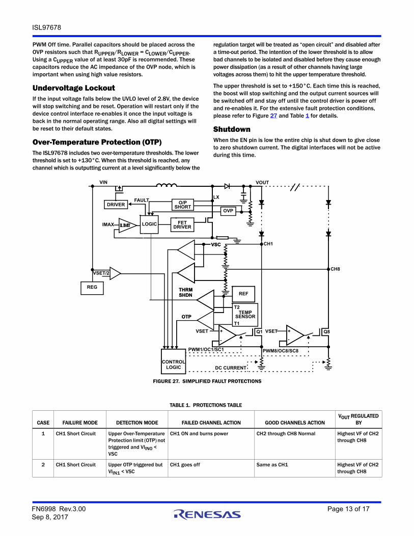
regulation target will be treated as “open circuit” and disabled after a time-out period. The intention of the lower threshold is to allow bad channels to be isolated and disabled before they cause enough power dissipation (as a result of other channels having large voltages across them) to hit the upper temperature threshold.
The upper threshold is set to +150°C. Each time this is reached, the boost will stop switching and the output current sources will be switched off and stay off until the control driver is power off and re-enables it. For the extensive fault protection conditions, please refer to Figure 27 and Table 1 for details.
Shutdown When the EN pin is low the entire chip is shut down to give close to zero shutdown current. The digital interfaces will not be active during this time.
TABLE 1. PROTECTIONS TABLE
CASE FAILURE MODE DETECTION MODE FAILED CHANNEL ACTION GOOD CHANNELS ACTIONVOUT REGULATED
BY
1 CH1 Short Circuit Upper Over-Temperature Protection limit (OTP) not triggered and VIIN0 < VSC
CH1 ON and burns power CH2 through CH8 Normal Highest VF of CH2 through CH8
2 CH1 Short Circuit Upper OTP triggered but VIIN1 < VSC
CH1 goes off Same as CH1 Highest VF of CH2 through CH8
FIGURE 27. SIMPLIFIED FAULT PROTECTIONS
Q8
VSC
CH8
VSET
DC CURRENT
PWM1/OC1/SC1
REF
FETDRIVER
LX
IMAX ILIMIT
DRIVERFAULT
OVP
VIN
T2
OTP
THRMSHDN
Q1
VSC CH1
VOUT
CONTROLLOGIC
VSET
PWM8/OC8/SC8
TEMPSENSOR
LOGIC
T1
OTP
THRMSHDN
O/PSHORT
+
-
+
-
REG
VSET/2
FN6998 Rev.3.00 Page 13 of 17Sep 8, 2017
ISL97678
Components SelectionsAccording to the inductor Voltage-Second Balance principle, the change of inductor current during the switching regulator On-time is equal to the change of inductor current during the switching regulator Off-time. The voltage across an inductor is as shown in Equation 6:
and IL @ On = IL @ Off, therefore:
where D is the switching duty cycle defined by the turn-on time over the switching periods. VD is Schottky diode forward voltage that can be neglected for approximation.
Rearranging the terms without accounting for VD gives the boost ratio and duty cycle respectively as Equations 8 and 9:
Input CapacitorSwitching regulators require input capacitors to deliver peak charging current and to reduce the impedance of the input supply. This reduces interaction between the regulator and input supply, thereby improving system stability. The high switching frequency of the loop causes almost all ripple current to flow in the input capacitor, which must be rated accordingly.
A capacitor with low internal series resistance should be chosen to minimize heating effects and improve system efficiency, such as X5R or X7R ceramic capacitors, which offer small size and a lower value of temperature and voltage coefficient compared to other ceramic capacitors.
It is recommended that an input capacitor of at least 10µF be used. Ensure the voltage rating of the input capacitor is suitable to handle the full supply range.
3 CH1 Short Circuit Upper OTP not triggered but VIIN1 > VSC
CH1 disabled after 6 PWM cycles time-out.
If 3 channels are already shut down, all channels will be shut down. Otherwise CH2-8 will remain as normal
Highest VF of CH2 through CH8
4 CH1 Open Circuit with infinite resistance
Upper OTP not triggered and VIIN1 < VSC
VOUT will ramp to OVP. CH1 will time-out after 6 PWM cycles and switch off. VOUT will drop to normal level.
CH2 through CH8 Normal Highest VF of CH2 through CH8
5 CH1 LED Open Circuit but has paralleled Zener
Upper OTP not triggered and VIIN1 < VSC
CH1 remains ON and has highest VF, thus VOUT increases
CH2 through CH8 ON, Q2 through Q8 burn power
VF of CH1
6 CH1 LED Open Circuit but has paralleled Zener
Upper OTP triggered but VIIN1 < VSC
CH1 goes off Same as CH1 VF of CH1
7 CH1 LED Open Circuit but has paralleled Zener
Upper OTP not triggered but VIIN1 > VSC
CH1 OFF CH2 through CH8 Normal Highest VF of CH2 through CH8
Upper OTP not triggered but VIINx > VSC
CH1 remains ON and has highest VF, thus VOUT increases.
VOUT increases then CH-X switches OFF. This is an unwanted shut off and can be prevented by setting OVP and/or VSC at an appropriate level.
VF of CH1
8 Channel-to-Channel VF too high
Lower OTP triggered but VIINx < VSC
Any channel at below the target current will fault out after 6 PWM cycles.Remaining channels driven with normal current.
Highest VF of CH1 through CH8
9 Channel-to-Channel VF too high
Upper OTP triggered but VIINx < VSC
All channels switched off Highest VF of CH1 through CH8
10 Output LED string voltage too high
VOUT > VOVP Driven with normal current. Any channel that is below the target current will time-out after 6 PWM cycles.
Highest VF of CH1 through CH8
11 VOUT/LX shorted to GND
LX will not switch
TABLE 1. PROTECTIONS TABLE (Continued)
CASE FAILURE MODE DETECTION MODE FAILED CHANNEL ACTION GOOD CHANNELS ACTIONVOUT REGULATED
BY
VL L IL t= (EQ. 6)
V I 0 L D tS VO VD VI–– = L 1 D tS–– (EQ. 7)
VO VI 1 1 D– = (EQ. 8)
D VO VI VO–= (EQ. 9)
FN6998 Rev.3.00 Page 14 of 17Sep 8, 2017
ISL97678
InductorThe selection of the inductor should be based on its maximum and saturation current (ISAT) characteristics, power dissipation (DCR), EMI susceptibility (shielded vs unshielded), and size. Inductor type and value influence many key parameters, including ripple current, current limit, efficiency, transient performance, and stability.
The inductor’s maximum current capability must be adequate enough to handle the peak current at the worst case condition. Additionally, if an inductor core is chosen with too low a current rating, saturation in the core will cause the effective inductor value to fall, leading to an increase in peak to average current level, poor efficiency and overheating in the core. The series resistance, DCR, within the inductor causes conduction loss and heat dissipation. A shielded inductor is usually more suitable for EMI susceptible applications, such as LED backlighting.
The peak current can be derived from the voltage across the inductor during the Off-period, as expressed in Equation 10:
The choice of 85% is an average term for the efficiency approximation. The first term is the average current, which is inversely proportional to the input voltage. The second term is the inductor current change, which is inversely proportional to L and fSW as a result, for a given switching.
ILpeak VO IO 85% VI 1 2 VI VO VI L VO fSW–+=
(EQ. 10)
FN6998 Rev.3.00 Page 15 of 17Sep 8, 2017
ISL97678
Intersil products are manufactured, assembled and tested utilizing ISO9001 quality systems as notedin the quality certifications found at www.intersil.com/en/support/qualandreliability.html
Intersil products are sold by description only. Intersil may modify the circuit design and/or specifications of products at any time without notice, provided that such modification does not, in Intersil's sole judgment, affect the form, fit or function of the product. Accordingly, the reader is cautioned to verify that datasheets are current before placing orders. Information furnished by Intersil is believed to be accurate and reliable. However, no responsibility is assumed by Intersil or its subsidiaries for its use; nor for any infringements of patents or other rights of third parties which may result from its use. No license is granted by implication or otherwise under any patent or patent rights of Intersil or its subsidiaries.
For information regarding Intersil Corporation and its products, see www.intersil.com
For additional products, see www.intersil.com/en/products.html
© Copyright Intersil Americas LLC 2009-2017. All Rights Reserved.All trademarks and registered trademarks are the property of their respective owners.
About IntersilIntersil Corporation is a leading provider of innovative power management and precision analog solutions. The company's products address some of the largest markets within the industrial and infrastructure, mobile computing, and high-end consumer markets.
For the most updated datasheet, application notes, related documentation, and related parts, see the respective product information page found at www.intersil.com.
For a listing of definitions and abbreviations of common terms used in our documents, visit www.intersil.com/glossary.
You can report errors or suggestions for improving this datasheet by visiting www.intersil.com/ask.
Reliability reports are also available from our website at www.intersil.com/support.
Revision HistoryThe revision history provided is for informational purposes only and is believed to be accurate, but not warranted. Please visit our website to make sure you have the latest revision.
DATE REVISION CHANGE
9/8/2017 FN6998.3 Added VHEADROOM_RANGE spec to the Electrical Specifications table.Added Note 11.In “Current Matching and Current Accuracy” on page 11, updated the second sentence in the second paragraph for clarification.Added Related Literature section.Applied new header/footer.
3/22/2014 FN6998.2 Changed PWM dimming “0.8%~100% duty cycle” to “0.4%~100% duty cycle” on the front page.Changed External PWM Input “25kHz” to “20kHz” in the Features section in order to be consistent with Electrical Specifications.Updated Application Circuit and Block Diagram drawings along with the resistor and capacitor names.Moved the VFSW specification to the BOOST SWITCHING REGULAR section of the Electrical Specifications table.Changed “/SHUT” to “EN” to be consistent with the Pin Descriptions table.Changed “ISET” to “RSET” for the LED current setting resistor to be consistent across the datasheet.Changed “VISET” to “VRSET” to be consistent with the RSET pin name.Changed “ROSC” to “RFSW” to be consistent across the datasheet.Changed “R1” and “R2” to “RUPPER” and “RLOWER”, respectively in OVP and VOUT Requirement section.Added FIGURE 1. TYPICAL APPLICATION CIRCUIT: TFT-LCD NOTEBOOK DISPLAY.Added FIGURE 25. MINIMUM 0.4% PWM DIMMING DUTY CYCLE.Updated “Package Outline Drawing” on page 17 to the latest revision.
11/5/09 FN6998.1 Changed VSC spec from “3.3min, 4.4max” to “3.3min, 4.6max”.
10/26/09 FN6998.0 Initial release
FN6998 Rev.3.00 Page 16 of 17Sep 8, 2017
ISL97678
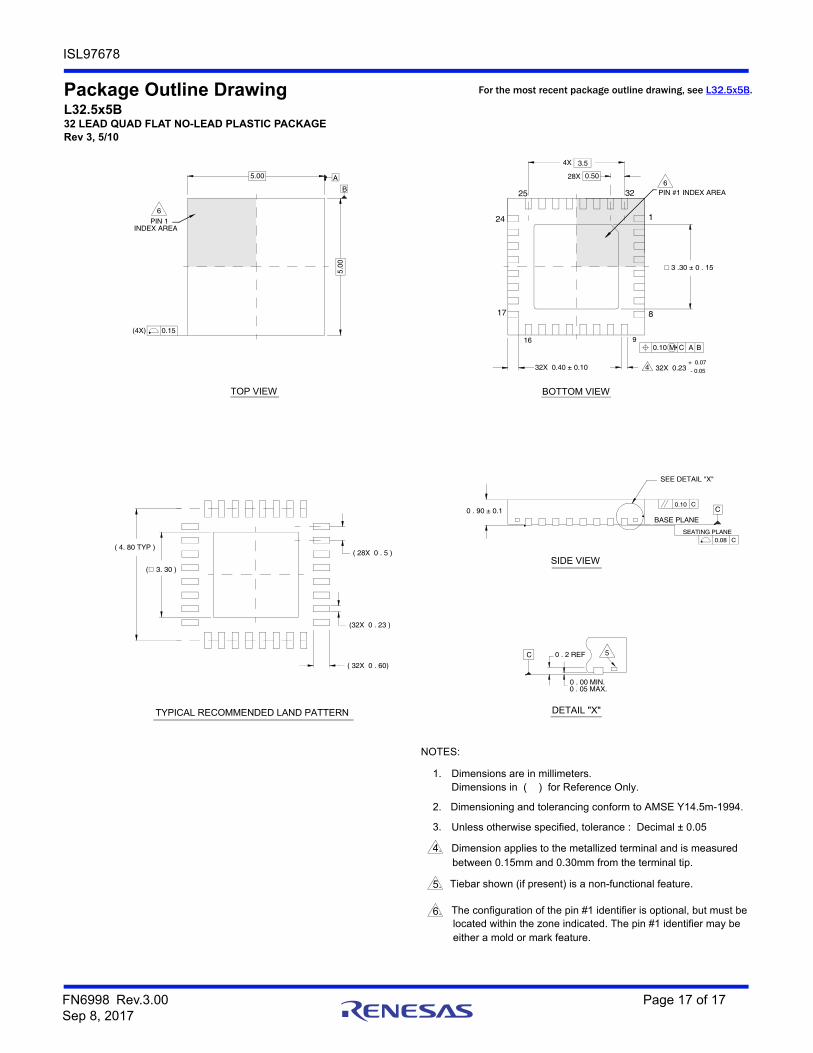
Package Outline DrawingL32.5x5B32 LEAD QUAD FLAT NO-LEAD PLASTIC PACKAGERev 3, 5/10
located within the zone indicated. The pin #1 identifier may be
Unless otherwise specified, tolerance : Decimal ± 0.05
Tiebar shown (if present) is a non-functional feature.
The configuration of the pin #1 identifier is optional, but must be
between 0.15mm and 0.30mm from the terminal tip.Dimension applies to the metallized terminal and is measured
Dimensions in ( ) for Reference Only.
Dimensioning and tolerancing conform to AMSE Y14.5m-1994.
6.
either a mold or mark feature.
3.
5.
4.
2.
Dimensions are in millimeters.1.
NOTES:
BOTTOM VIEW
DETAIL "X"
SIDE VIEW
TYPICAL RECOMMENDED LAND PATTERN
TOP VIEW
5.00 A
5.00
B
INDEX AREAPIN 1
6
(4X) 0.15
32X 0.40 ± 0.10 4
A
32X 0.23
M0.10 C B16 9
4X
0.5028X
3.5
6PIN #1 INDEX AREA
3 .30 ± 0 . 15
0 . 90 ± 0.1BASE PLANE
SEE DETAIL "X"
SEATING PLANE
0.10 CC
0.08 C
0 . 2 REFC
0 . 05 MAX.0 . 00 MIN.
5
( 3. 30 )
( 4. 80 TYP )( 28X 0 . 5 )
(32X 0 . 23 )
( 32X 0 . 60)
+ 0.07
- 0.05
17
25
24
8
1
32
For the most recent package outline drawing, see L32.5x5B.
FN6998 Rev.3.00 Page 17 of 17Sep 8, 2017