idt74sstubf32869a 7093 9 - renesas.com
TRANSCRIPT

DATASHEET
14-BIT CONFIGURABLE REGISTERED BUFFER FOR DDR2 CONFIDENTIAL IDT74SSTUBF32869A
14-BIT CONFIGURABLE REGISTERED BUFFER FOR DDR2 1 IDT74SSTUBF32869A 7093/10
CONFIDENTIAL
Description
The IDT74SSTUBF32869A is 14-bit 1:2 registered buffer with parity, designed for 1.7 V to 1.9 V VDD operation.
All clock and data inputs are compatible with the JEDEC standard for SSTL_18. The control inputs are LVCMOS. All outputs are 1.8V CMOS drivers optimized to drive the DDR2 DIMM load. They provide 50% more dynamic driver strength than the standard SSTU32864 outputs.
The IDT74SSTUBF32869A operates from a differential clock (CLK and CLK). Data are registered at the crossing of CLK going high, and CLK going low.
The device supports low-power standby operation. When the reset input (RESET) is low, the differential input receivers are disabled, and undriven (floating) data, clock and reference voltage (VREF) inputs are allowed. In addition, when RESET is low all registers are reset, and all outputs except PTYERR are forced low. The LVCMOS RESET input must always be held at a valid logic high or low level.
To ensure defined outputs from the register before a stable clock has been supplied, RESET must be held in the low state during power up.
In the DDR2 RDIMM application, RESET is specified to be completely asynchronous with respect to CLK and CLK. Therefore, no timing relationship can be guaranteed between the two. When entering reset, the register will be cleared and the outputs will be driven low quickly, relative to the time to disable the differential input receivers. However, when coming out of reset, the register will become active quickly, relative to the time to enable the differential input receivers. IDT74SSTUBF32869A must ensure that the outputs remain low as long as the data inputs are low, the clock is stable during the time from the low-to-high transition of RESET and the input receivers are fully enabled. This will ensures that there are no glitches on the output.
The device monitors both DCS and CSR inputs and will gate the Qn, PPO (Paritial-Parity-Out) and PTYERR (Parity Error) Parity outputs from changing states when both DCS and CSR are high. If either DCS and CSR input is low, the Qn, PPO and PTYERR outputs will function normally. The RESET input has priority over the DCS and CSR controls and will force the Qn and PPO outputs low and the PTYERR high.
The IDT74SSTUBF32869A includes a parity checking function. The IDT74SSTUBF32869A accepts a parity bit from the memory controller at its input pin PARIN one or two cycles after the corresponding data input, compares it with the data received on the D-inputs and indicates on its opendrain PTYERR pin (active low) whether a parity error has occurred. The number of cycles depends on the setting of C1.
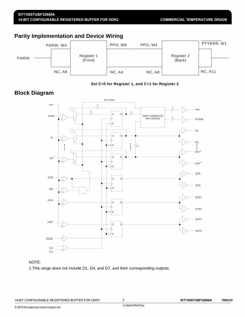
When used as a single device, the C1 input is tied low. When used in pairs, the C1 inputs is tied low for the first register (front) and the C1 input is tied high for the second register. When used as a single register, the PPO and PTYERR signals are produced two clock cycles after the corresponding data input. When used in pairs, the PTYERR signals of the first register are left floating. The PPO outputs of the first register are cascaded to the PARIN signas on the second register (back). The PPO and PTYERR signals of the second register are produced three clock cycles after the corresponding data input. Parity implimentation and device wiring for single and dual die is described in the diagram below.
If an error occurs, and the PTYERR is driven low, it stays low for two clock cycles or until RESET is driven low. The DIMM-dependent signals (DCKE, DCS, CSR and DODT) are not included in the parity check computations.
All registers used on an individual DIMM must be of the same configuration, i.e single or dual die.
Features
• 14-bit 1:2 registered buffer with parity check functionality• Supports SSTL_18 JEDEC specification on data inputs
and outputs• 50% more dynamic driver strength than standard
SSTU32864• Supports LVCMOS switching levels on C1 and RESET
inputs• Low voltage operation: VDD = 1.7V to 1.9V• Available in 150 BGA package
Applications
• DDR2 Memory Modules• Provides complete DDR DIMM solution with
ICS98ULPA877A or IDTCSPUA877A• Ideal for DDR2 667 and 800
IDT74SSTUBF32869A14-BIT CONFIGURABLE REGISTERED BUFFER FOR DDR2 COMMERCIAL TEMPERATURE GRADE
14-BIT CONFIGURABLE REGISTERED BUFFER FOR DDR2 2 IDT74SSTUBF32869A 7093/10
CONFIDENTIAL
Parity Implementation and Device Wiring
Block Diagram
NOTE:
1.This range does not include D1, D4, and D7, and their corresponding outputs.
Register 1(Front)
Register 2(Back)PARIN
PARIN, W4
NC, A8
PPO, W8
NC, A4
PTYERR, W1
NC, A11
PPO, W4
NC, A8
Set C=0 for Register 1, and C=1 for Register 2
PPO
RESET
CLK
CLK
DODTQODTA
QODTB
QCKEA
QCKEB
R
D Q
R
D Q
DCKE
PTYERR
R
D Q
Q14A
Q14B
Q1A
Q1B
R
D Q
R
D Q
VREF
PARITY GENERATORAND CHECKER
QCSA
QCSB
R
D Q
PARIN
D1
D14
DCS0
11
2
2 2
CSR
(CS Active)
2
2
(1)
(1)
(1)

IDT74SSTUBF32869A14-BIT CONFIGURABLE REGISTERED BUFFER FOR DDR2 COMMERCIAL TEMPERATURE GRADE
14-BIT CONFIGURABLE REGISTERED BUFFER FOR DDR2 3 IDT74SSTUBF32869A 7093/10
CONFIDENTIAL
Block Diagram
NOTE:
1.PARIN is used to generate PPO and PTYERR.
RESET
CLK
CLK
D2 - D3,D5 - D6,D8 - D14
VREF
CED
CLK
R
CE
ParityCheck
11
0
1D
CLK
R
D
CLK
R
2
2
PPO
PTYERRPARIN2
CLK
R
2-BitCounter D
CLK
R
0
1
C1, C2
CE
11
D2 - D3,D5 - D6,D8 - D25
LPS0(Internal Node)
11 Q2 A- Q3A,Q5A - Q6A,Q8A - Q14A
D2 - D3,D5 - D6,D8 - D1411
CED
CLK
RCE
11 Q2B - Q3B,Q5B - Q6B,Q8B - Q14B

IDT74SSTUBF32869A14-BIT CONFIGURABLE REGISTERED BUFFER FOR DDR2 COMMERCIAL TEMPERATURE GRADE
14-BIT CONFIGURABLE REGISTERED BUFFER FOR DDR2 4 IDT74SSTUBF32869A 7093/10
CONFIDENTIAL
Pin Configuration
150-Ball BGATOP VIEW
NOTE:
1.NC denotes a no-connect (ball present but not connected to the die). NB indicates no ball is populated at thatgridpoint.
A
B
C
D
E
F
VDD GND VREF VDD
VDDGND
NB
QCKEA
Q2A
VDD NB
NB VDD GND GND NB VDDGNDVDD
Q3A
GND
GND
QODTA
VDD D3 NC
NB
VDD
VDD NB DCKE NB D2 NB
QCKEB
DODT
1 2 3 4 5 6 7 8 9 10 11
G
H
J
K
L
M
VDD D6
CSR
D5Q5A
QCSA
VDD
NB NC
D10
NB NBQ6A
Q8A
Q9A
VDD DCS
NB
VDD
VDD
NC
GND GND
D8
NB
N
P
R
T
V
W
VDD NBD9Q10A
Q12A
VDD MCL(1)
GND VREF
VDDQ11A
VDD
PTYERR
NB VDD GND GND
PARIN
C1 D11 NB
GND
GND
GND
Q13A VDD
NB NC
GND
NB GND NB GND NB GND NB VDD
U Q14A VDD NB
GND
NB
GND
GND
GND
NB
GND
NB
GND
GND
NB
GND
NB
GND NB
D13
NC
NB
NB
NB
NB
NB
NC NB
CLK
NB
RESET
NB
CLK
NC
NB
NB
NC
NB
NB
D14
NC
NB
NB
NC
NC
NB
NB
NB
NB
NB
NC
NB
NB
D12
NB
GND
GND
PPO
GND
GND
NB
GND
GND
VDD
NB
NB
GND
GND
GND
GND
NB
NB
VDD
VDD
NB
VDD
VDD
VDD
VDD
VDD
VDD
NB
VDD
VDD
NB
VDD
VDD
C1
VDD Q2B
Q3B
QODTB
Q5B
Q6B
QCSB
VDD
Q8B
Q9B
Q10B
Q11B
Q12B
Q13B
Q14B
VDD
NB
GND
MCL(1)
MCL(1)
NCNCNCMCL(1)

IDT74SSTUBF32869A14-BIT CONFIGURABLE REGISTERED BUFFER FOR DDR2 COMMERCIAL TEMPERATURE GRADE
14-BIT CONFIGURABLE REGISTERED BUFFER FOR DDR2 5 IDT74SSTUBF32869A 7093/10
CONFIDENTIAL
150 Ball CTBGA Package Attributes
A
B
C
D
E
F
G
H
J
K
L
M
N
P
R
T
U
V
W
1 2 3 4 5 6 7 8 9 10 11
TOP VIEW
Top Marking
N
P
R
T
U
V
G
H
J
K
L
M
A
B
C
D
E
F
W
1234567891011
BOTTOM VIEW
SIDE VIEW

IDT74SSTUBF32869A14-BIT CONFIGURABLE REGISTERED BUFFER FOR DDR2 COMMERCIAL TEMPERATURE GRADE
14-BIT CONFIGURABLE REGISTERED BUFFER FOR DDR2 6 IDT74SSTUBF32869A 7093/10
CONFIDENTIAL
Function Table
Inputs1 Outputs
RESET DCS CSR CLK CLK Dn, DODT, DCKE Qn QCS QODT, QCKE
H L L ↑ ↓ L L L L
H L L ↑ ↓ H H L H
H L L L or H L or H X Q02 Q0
2 Q02
H L H ↑ ↓ L L L L
H L H ↑ ↓ H H L H
H L H L or H L or H X Q02 Q0
2 Q02
H H L ↑ ↓ L L H L
H H L ↑ ↓ H H H H
H H L L or H L or H X Q02 Q0
2 Q02
H H H ↑ ↓ L Q02 H L
H H H ↑ ↓ H Q02 H H
H H H L or H L or H X Q02 Q0
2 Q02
L X or Floating
X or Floating
X or Floating
X or Floating
X or Floating L L L
1 H = HIGH Voltage LevelL = LOW Voltage LevelX = Don’t Care↑ = LOW to HIGH↓ = HIGH to LOW
2 Output Level before the indicated steady-state conditions were established.

IDT74SSTUBF32869A14-BIT CONFIGURABLE REGISTERED BUFFER FOR DDR2 COMMERCIAL TEMPERATURE GRADE
14-BIT CONFIGURABLE REGISTERED BUFFER FOR DDR2 7 IDT74SSTUBF32869A 7093/10
CONFIDENTIAL
Terminal FunctionsSignal Group
Terminal Name
Type Description
Ungated Inputs
DCKE, DODT SSTL_18 DRAM function pins not associated with Chip Select
Chip Select Gated Inputs
D1...D141
1 This range does not include D1, D4, and D7, and their corresponding outputs.
SSTL_18 DRAM inputs, re-driven only when Chip Select is LOW
Chip Select Inputs
DCS, CSR SSTL_18DRAM Chip Select signals. These pins initiate DRAM address/command decodes, and as such at least one will be LOW when a valid address/command is present.
Re-Driven Outputs
Q1A...Q14A1, Q1B...Q14B1,
QCSnA, B QCKEnA, B QODTnA, B
SSTL_18Outputs of the register, valid after the specified clock count and immediately following a rising edge of the clock
Parity Input PARIN SSTL_18Input parity is received on pin PARIN, and should maintain odd parity across the D1:D14 inputs, at the rising edge of the clock, one cycle after Chip Select is LOW.
Parity Output PPO SSTL_18 Partial Parity Output. Indicates parity out of D1-D14.
Parity Error Output
PTYERROpen Drain
When LOW, this output indicates that a parity error was identified associated with the address and/or command inputs. PTYERR will be active for two clock cycles, and delayed by in total two clock cycles for compatibility with final parity out timing on the industry-standard DDR2 register with parity (in JEDEC definition).
Configuration Inputs
C1 SSTL_18When LOW, the register is configured as Register 1. When HIGH, the register is configured as Register 2.
Clock Inputs CLK, CLK SSTL_18Differential master clock input pair to the register. The register operation is triggered by a rising edge on the positive clock input (CLK).
Miscellaneous Inputs
RESETSSTL_18
Input
Asynchronous Reset Input. When LOW, it causes a reset of the internal latches, thereby forcing the outputs LOW. RESET also resets the PTYERR signal.
VREF 0.9V nominalInput reference voltage for SSTL_18 inputs. Two pins (internally tied together) are used for increased Inputsreliability.
VDD Power Input Power Supply Voltage
GND Ground Input Ground

IDT74SSTUBF32869A14-BIT CONFIGURABLE REGISTERED BUFFER FOR DDR2 COMMERCIAL TEMPERATURE GRADE
14-BIT CONFIGURABLE REGISTERED BUFFER FOR DDR2 8 IDT74SSTUBF32869A 7093/10
CONFIDENTIAL
Parity and Standby Function Table
Inputs1 Outputs
RESET DCS CSR CLK CLK Σ of Inputs = H (D1 - D14)2
PARIN3 PPO PTYERR4
H L X ↑ ↓ Even L L H
H L X ↑ ↓ Odd L H L
H L X ↑ ↓ Even H H L
H L X ↑ ↓ Odd H L H
H L L ↑ ↓ Even L L H
H L L ↑ ↓ Odd L H L
H L L ↑ ↓ Even H H L
H L L ↑ ↓ Odd H L H
H H H ↑ ↓ X X PPOn0 PTYERRn0
H X X L or H L or H X X PPOn0 PTYERRn0
L X or Floating
X or Floating
X or Floating
X or Floating
X or Floating X or Floating L H
1 H = HIGH Voltage LevelL = LOW Voltage LevelX = Don’t Care↑ = LOW to HIGH↓ = HIGH to LOW
2 This range does not include D1, D4, and D7.3 PARIN arrives one clock cycle (C1 = 0), or two clock cycles (C1 = 1), after the data to which it applies.4 This transition assumes PTYERR is HIGH at the crossing of CLK going HIGH and CLK going LOW. IfPTYERR is LOW, it stays latched LOW for two clock cycles or until RESET is driven LOW. PARIN is used togenerate PPO and PTYERR.

IDT74SSTUBF32869A14-BIT CONFIGURABLE REGISTERED BUFFER FOR DDR2 COMMERCIAL TEMPERATURE GRADE
14-BIT CONFIGURABLE REGISTERED BUFFER FOR DDR2 9 IDT74SSTUBF32869A 7093/10
CONFIDENTIAL
Absolute Maximum Ratings
Stresses greater than those listed under ABSOLUTE MAXIMUM RATINGS may cause permanent damage to the device. This is a stress rating only and functional operation of the device at these or any other conditions above those indicated in the operational sections of this specification is not implied. Exposure to absolute maximum rating conditions for extended periods may affect reliability.
Mode Select
Output Buffer CharacteristicsOutput edge rates over recommended operating free-air temperature range
Item RatingSupply Voltage, VDD -0.5V to 2.5V
Input Voltage Range, VI1
1 The input and output negative voltage ratings may be exceeded if the ratings of the I/P andO/P clamp current are observed.
-0.5V to VDD + 2.5V
Output Voltage Range, VO1,2
2 This current will flow only when the output is in the high state level VO > VDDQ.
-0.5V to VDDQ + 0.5V
Input Clamp Current, IIK ±50mA
Output Clamp Current, IOK ±50mA
Continuous Output Clamp Current, IO ±50mA
Continuous Current through each VDD or GND ±100mA
Package Thermal Impedance (θja)3
3 The package thermal impedance is calculated in accordance with JESD 51.
0m/s Airflow 40° C/W
1m/s Airflow 29° C/W
Storage Temperature, TSTG -65 to +150° C
C1 Device Mode0 First device in pair, Front
1 Second device in pair, Back
Parameter
VDD = 1.8V ± 0.1V
UnitsMin. Max.dV/dt_r 1 4 V/ns
dV/dt_f 1 4 V/ns
dV/dt_∆1
1 Difference between dV/dt_r (rising edge rate) and dV/dt_f (falling edge rate).
1 V/ns

IDT74SSTUBF32869A14-BIT CONFIGURABLE REGISTERED BUFFER FOR DDR2 COMMERCIAL TEMPERATURE GRADE
14-BIT CONFIGURABLE REGISTERED BUFFER FOR DDR2 10 IDT74SSTUBF32869A 7093/10
CONFIDENTIAL
Operating Characteristics, TA = 25° CThe RESET and Cn inputs of the device must be held at valid levels (not floating) to ensure proper device operation. The differential inputs must not be floating unless RESET is LOW.
Symbol Parameter Min. Typ. Max. Units
VDD I/O Supply Voltage 1.7 1.8 1.9 V
VREF Reference Voltage 0.49 * VDD 0.5 * VDD 0.51 * VDD V
VTT Termination Voltage VREF - 0.04 VREF VREF + 0.04 V
VI Input Voltage 0 VDD V
VIH AC High-Level Input VoltageDn, PARIN, DCS, CSR,
DCKEn, DODTn
VREF + 0.25
VVIL AC Low-Level Input Voltage VREF - 0.25
VIH DC High-Level Input Voltage VREF + 0.125
VIL DC Low-Level Input Voltage VREF - 0.125
VIH High-Level Input VoltageRESET, C1
0.65 * VDDQV
VIL Low-Level Input Voltage 0.35 * VDDQ
VICR Common Mode Input RangeCLK, CLK
0.675 1.125 V
VID Differential Input Voltage 600 mV
IOH High-Level Output Current -12mA
IOL Low-Level Output Current 12
IERROL PTYERR Low-Level Output Current 25 mA
TA Operating Free-Air Temperature 0 +70 ° C

IDT74SSTUBF32869A14-BIT CONFIGURABLE REGISTERED BUFFER FOR DDR2 COMMERCIAL TEMPERATURE GRADE
14-BIT CONFIGURABLE REGISTERED BUFFER FOR DDR2 11 IDT74SSTUBF32869A 7093/10
CONFIDENTIAL
DC Electrical Characteristics Over Operating RangeFollowing Conditions Apply Unless Otherwise Specified:
Operating Condition: TA = 0°C to +70°C, VDDQ/VDD = 1.8V ± 0.1V.
Symbol Parameter Test Conditions Min. Typ. Max. Units
VIK II = -18mA -1.2 V
VOHVDDQ = 1.7V, IOH = -100µA VDDQ-0.2
VVDDQ = 1.7V, IOH = -12mA 1.2
VOLVDDQ = 1.7V, IOL = 100µA 0.2
VVDDQ = 1.7V, IOL = 12mA 0.5
VERROLPTYERR Output Low Voltage
IERROL = 25mA; VDD = 1.7V 0.5 V
IIL All Inputs VI = VDD or GND -5 +5 µA
IDD
Static Standby IO = 0, VDD = 1.9V, RESET = GND 200 µA
Static Operating
IO = 0, VDD = 1.9V, RESET = VDD, VI = VIH(AC) or VIL(AC), CLK = CLK = VIH(AC) or VIL(AC)
10
mAIO = 0, VDD = 1.9V, RESET = VDD, VI = VIH(AC) or VIL(AC), CLK = VIH(AC), CLK = VIL(AC)
140
IDDD
Dynamic Operating (clock only)
IO = 0, VDD = 1.8V, RESET = VDD, VI = VIH(AC) or VIL(AC), CLK and CLK switching 50% duty cycle
247µA/Clock
MHz
Dynamic Operating (per each data input)
IO = 0, VDD = 1.8V, RESET = VDD, VI = VIH(AC) or VIL(AC), CLK and CLK switching 50% duty cycle. One data input switching at half clock frequency, 50% duty cycle.
52µA/Clock
MHz/ Data
CIN
Dn, PARIN, DSCn inputs
VI = VREF ± 250mV 2 3
pFCLK and CLK inputs
VICR = 0.9V, VIPP = 600mV 3.5 4.5
RESET VI = VDD or GND 4.5

IDT74SSTUBF32869A14-BIT CONFIGURABLE REGISTERED BUFFER FOR DDR2 COMMERCIAL TEMPERATURE GRADE
14-BIT CONFIGURABLE REGISTERED BUFFER FOR DDR2 12 IDT74SSTUBF32869A 7093/10
CONFIDENTIAL
Timing Requirements Over Recommended Operating Free-Air Temperature Range
Switching Characteristics Over Recommended Free Air Operating Range (unless otherwise noted)
Symbol Parameter
VDD = 1.8V ± 0.1V
UnitsMin. Max.
fCLOCK Clock Frequency 410 MHz
tW Pulse Duration, CLK, CLK HIGH or LOW 1 ns
tACT1
1 VREF must be held at a valid input voltage level and data inputs must be held at valid logic levels for aminimum time of tACT(max) after RESET is taken HIGH.
Differential Inputs Active Time 10 ns
tINACT2
2 VREF, data, and clock inputs must be held at a valid input voltage levels (not floating) for a minimumtime of tINACT(max) after RESET is taken LOW.
Differential Inputs Inactive Time 15 ns
tSUSetup Time
DCS before CLK↑ , CLK↓, CSR HIGH; CSR before CLK↑ , CLK↓, DCS HIGH
0.6
nsDCS before CLK↑ , CLK↓, CSR LOW 0.5
DODT, DOCKE, and data before CLK↑ , CLK↓ 0.5
PAR_IN before CLK↑ , CLK↓ 0.5
tHHold Time
DCS, DODT, DCKE, and data after CLK↑ , CLK↓ 0.4ns
PAR_IN after CLK↑ , CLK↓ 0.4
Symbol Parameter
VDD = 1.8V ± 0.1V
UnitsMin. Max.fMAX Max Input Clock Frequency 340 MHz
tPDM1
1 Design target as per JEDEC specifications.
Propagation Delay, single-bit switching, CLK↑ / CLK↓ to Qn 1.1 1.5 ns
tPD2
2 Production Test. (See Production Test Circuit in TEST CIRCUIT AND WAVEFORM section.)
Propagation Delay, single-bit switching, CLK↑ / CLK↓ to Qn 0.4 0.8 ns
tPDMSS1 Propagation Delay, simultaneous switching, CLK↑ / CLK↓ to Qn 1.6 ns
tLH LOW to HIGH Propagation Delay, CLK↑ / CLK↓ to PTYERR 1.2 3 ns
tHL HIGH to LOW Propagation Delay, CLK↑ / CLK↓ to PTYERR 0.4 3 ns
tPD Propagation Delay from CLK↑ / CLK↓ to PPO 0.5 1.6 ns
tPHL HIGH to LOW Propagation Delay, RESET↓ to Qn↓ 3 ns
tPLH LOW to HIGH Propagation Delay, RESET↓ to PTYERR↑ 3 ns
IDT74SSTUBF32869A14-BIT CONFIGURABLE REGISTERED BUFFER FOR DDR2 COMMERCIAL TEMPERATURE GRADE
14-BIT CONFIGURABLE REGISTERED BUFFER FOR DDR2 13 IDT74SSTUBF32869A 7093/10
CONFIDENTIAL
Output Buffer Characteristics
Output edge rates over recommended operating free-air temperature range
Parameter
VDD = 1.8V ± 0.1V
UnitsMin. Max.
dV/dt_r 1 4 V/ns
dV/dt_f 1 4 V/ns
dV/dt_∆1
1 Difference between dV/dt_r (rising edge rate) and dV/dt_f (falling edge rate).
1 V/ns

IDT74SSTUBF32869A14-BIT CONFIGURABLE REGISTERED BUFFER FOR DDR2 COMMERCIAL TEMPERATURE GRADE
14-BIT CONFIGURABLE REGISTERED BUFFER FOR DDR2 14 IDT74SSTUBF32869A 7093/10
CONFIDENTIAL
Register Timing
NOTES:
1.This range does not include D1, D4, and D7, and their corresponding outputs.
2.PARIN is used to generate PPO and PTYERR.
RESET
DCS
CSR
CLK
CLK
D1 - D14
Q1 - Q14
PARIN
PPO
PTYERR
n n + 1 n + 2 n + 3 n + 4
tSU tH
tPDCLK to Q
tSU tH
tPD
tPDCLK to PPO
CLK to PTYERRtPD
(2)
(2)
(2)
CLK to PTYERR
(1)
(1)

IDT74SSTUBF32869A14-BIT CONFIGURABLE REGISTERED BUFFER FOR DDR2 COMMERCIAL TEMPERATURE GRADE
14-BIT CONFIGURABLE REGISTERED BUFFER FOR DDR2 15 IDT74SSTUBF32869A 7093/10
CONFIDENTIAL
Register Timing
NOTES:
1.This range does not include D1, D4, and D7, and their corresponding outputs.
2.PARIN is used to generate PPO and PTYERR.
RESET
DCS
CSR
CLK
CLK
D1 - D14
Q1 - Q14
PPO(not used)
n n + 1 n + 2 n + 3 n + 4
tSU tH
tPDCLK to Q
tSU tH
tPD
tPDCLK to PPO
tPD
PARIN
(2)
(2)
(2)
PTYERR CLK to PTYERR CLK to PTYERR
(1)
(1)

IDT74SSTUBF32869A14-BIT CONFIGURABLE REGISTERED BUFFER FOR DDR2 COMMERCIAL TEMPERATURE GRADE
14-BIT CONFIGURABLE REGISTERED BUFFER FOR DDR2 16 IDT74SSTUBF32869A 7093/10
CONFIDENTIAL
Test Circuits and Waveforms (VDD = 1.8V ± 0.1V)
Simulation Load Circuit
Voltage and Current Waveforms Inputs Active and Inactive Times
Voltage Waveforms - Pulse Duration
Voltage Waveforms - Setup and Hold Times
Production-Test Load Circuit
Voltage Waveforms - Propagation Delay Times
Voltage Waveforms - Propagation Delay Times
NOTES:1. CL includes probe and jig capacitance.2. IDD tested with clock and data inputs held at VDD or GND, and Io = 0mA3. All input pulses are supplied by generators having the following characteristics: PRR ≤10MHz, Zo = 50Ω, input slew rate = 1 V/ns ±20% (unless otherwise specified).4. The outputs are measured one at a time with one transition per measurement.5. VTT = VREF = VDD/26. VIH = VREF + 250mV (AC voltage levels) for differential inputs. VIH = VDD for LVCMOS input.7. VIL = VREF - 250mV (AC voltage levels) for differential inputs. VIL = GND for LVCMOS input.8. VID = 600mV.9. tPLH and tPHL are the same as tPDM.
CL = 30 pF RL = 1K
DUT
Out
RL = 100
CLK Inputs
TL = 50 TL = 350ps, 50 Test Point
CLKCLK
VDD
RL = 1K
Test Point
Test Point
VDD
0V
VDD/2
LVCMOSRESET
Input
IDD
VDD/2
tINACT tACT
10%
90%
VICR VIDVICRInput
tW
VREF
VIH
VILVREFInput
VICR VID
tSU tH
CLK
CLK
ZO = 50 TestPoint
RL = 50 DUT
OutCLK Inputs
CLK
VDD/2
CLKZO = 50
ZO = 50
TestPoint
TestPoint
CLKVICR VID
tPLH tPHL
OutputVOH
VOL
VICR
VTT VTT
CLK
VOH
VOL
VIH
VIL
tRPHL
VDD/2
VTT
LVCMOSRESET
Input
Output

IDT74SSTUBF32869A14-BIT CONFIGURABLE REGISTERED BUFFER FOR DDR2 COMMERCIAL TEMPERATURE GRADE
14-BIT CONFIGURABLE REGISTERED BUFFER FOR DDR2 17 IDT74SSTUBF32869A 7093/10
CONFIDENTIAL
Test Circuits and Waveforms (VDD = 1.8V ± 0.1V)
Load Circuit: High-to-Low Slew-Rate Adjustment
Voltage Waveforms: High-to-Low Slew-Rate Adjustment
Load Circuit: Low-to-High Slew-Rate Adjustment
Voltage Waveforms: Low-to-High Slew-Rate Adjustment
Load Circuit: Error Output Measurements
Voltage Waveforms: Open Drain Output Low-to-High Transition Time (with respect to RESET input)
Voltage Waveforms: Open Drain Output High-to-Low Transition Time (with respect to clock inputs)
Voltage Waveforms: Open Drain Output Low-to-High Transition Time (with respect to clock inputs)
NOTES:
1. CL includes probe and jig capacitance.
2. All input pulses are supplied by generators having the following characteristics: PRR ≤10MHz, Zo = 50Ω, inputslew rate = 1 V/ns ±20% (unless otherwise specified).
CL = 10 pF
RL = 50 DUT
Out Test Point
VDD
VOH80%
20%VOL
Output
dv_fdt_f
CL = 10 pFRL = 50
DUT
Out Test Point
VOL20%
80%VOH
Output
dv_rdt_r
CL = 10 pF
RL = 1K DUT
Out Test Point
VDD
VOH
VCC
OutputWaveform 2
LVCMOSRESET
Input
tPLH
VCC/2
0.15V0V
0V
VCC
VICR
tHL
TimingInputs VICR VI(PP)
OutputWaveform 1
VCC/2VOL
VOH
OutputWaveform 2
0.15V0V
VICR
tHL
TimingInputs VICR VI(PP)
IDT74SSTUBF32869A14-BIT CONFIGURABLE REGISTERED BUFFER FOR DDR2 COMMERCIAL TEMPERATURE GRADE
14-BIT CONFIGURABLE REGISTERED BUFFER FOR DDR2 18 IDT74SSTUBF32869A 7093/10
CONFIDENTIAL
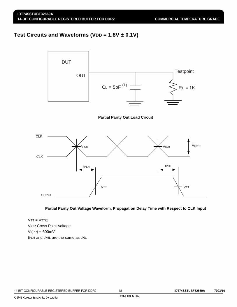
Test Circuits and Waveforms (VDD = 1.8V ± 0.1V)
Partial Parity Out Load Circuit
Partial Parity Out Voltage Waveform, Propagation Delay Time with Respect to CLK Input
VTT = VTT/2
VICR Cross Point Voltage
VI(PP) = 600mV
tPLH and tPHL are the same as tPD.
DUT
OUT
CL = 5pF (1)
Testpoint
RL = 1K
CLK
CLK
VICR VICR VI(PP)
tPLH tPHL
VTT VTT
Output

IDT74SSTUBF32869A14-BIT CONFIGURABLE REGISTERED BUFFER FOR DDR2 COMMERCIAL TEMPERATURE GRADE
14-BIT CONFIGURABLE REGISTERED BUFFER FOR DDR2 19 IDT74SSTUBF32869A 7093/10
CONFIDENTIAL
Application Information
The typical values below are measured on standard JEDEC raw cards, using the JEDEC DDR2 register validation board running patterns 0x43, 0x4F, and 0x5A.
Raw Card Values
Raw Card1
1 All values are valid under nominal conditions and minimum/maximum of typical sig-nals on one typical DIMM. Measurements include all jitter and ISI effects.
tPDMSS Overshoot UndershootW 1.48 446 444

IDT74SSTUBF32869A14-BIT CONFIGURABLE REGISTERED BUFFER FOR DDR2 COMMERCIAL TEMPERATURE GRADE
14-BIT CONFIGURABLE REGISTERED BUFFER FOR DDR2 20 IDT74SSTUBF32869A 7093/10
CONFIDENTIAL
Ordering InformationXXX XX
PackageDevice Type
BKG Low Profile, Fine Pitch, Ball Grid Array
14-Bit Configurable Registered Buffer for DDR2869A
32 Double Density
IDT74SSTUBF XXFamily Shipping
Carrier
X
8 Tape and Reel

© 2006 Integrated Device Technology, Inc. All rights reserved. Product specifications subject to change without notice. IDT and the IDT logo are trademarks of Integrated DeviceTechnology, Inc. Accelerated Thinking is a service mark of Integrated Device Technology, Inc. All other brands, product names and marks are or may be trademarks or registeredtrademarks used to identify products or services of their respective owners. Printed in USA
Corporate HeadquartersIntegrated Device Technology, Inc.6024 Silver Creek Valley RoadSan Jose, CA 95138United States800 345 7015+408 284 8200 (outside U.S.)
Asia Pacific and JapanIntegrated Device Technology Singapore (1997) Pte. Ltd.Reg. No. 199707558G435 Orchard Road #20-03 Wisma AtriaSingapore 238877+65 6 887 5505
EuropeIDT Europe, LimitedPrime HouseBarnett Wood LaneLeatherhead, SurreyUnited Kingdom KT22 7DE+44 1372 363 339
For Sales800-345-7015408-284-8200Fax: 408-284-2775
Innovate with IDT and accelerate your future networks. Contact:
www.IDT.com
IDT74SSTUBF32869A14-BIT CONFIGURABLE REGISTERED BUFFER FOR DDR2 COMMERCIAL TEMPERATURE GRADE

Corporate HeadquartersTOYOSU FORESIA, 3-2-24 Toyosu,Koto-ku, Tokyo 135-0061, Japanwww.renesas.com
Contact InformationFor further information on a product, technology, the most up-to-date version of a document, or your nearest sales office, please visit:www.renesas.com/contact/
TrademarksRenesas and the Renesas logo are trademarks of Renesas Electronics Corporation. All trademarks and registered trademarks are the property of their respective owners.
IMPORTANT NOTICE AND DISCLAIMER
RENESAS ELECTRONICS CORPORATION AND ITS SUBSIDIARIES (“RENESAS”) PROVIDES TECHNICAL SPECIFICATIONS AND RELIABILITY DATA (INCLUDING DATASHEETS), DESIGN RESOURCES (INCLUDING REFERENCE DESIGNS), APPLICATION OR OTHER DESIGN ADVICE, WEB TOOLS, SAFETY INFORMATION, AND OTHER RESOURCES “AS IS” AND WITH ALL FAULTS, AND DISCLAIMS ALL WARRANTIES, EXPRESS OR IMPLIED, INCLUDING, WITHOUT LIMITATION, ANY IMPLIED WARRANTIES OF MERCHANTABILITY, FITNESS FOR A PARTICULAR PURPOSE, OR NON-INFRINGEMENT OF THIRD PARTY INTELLECTUAL PROPERTY RIGHTS.
These resources are intended for developers skilled in the art designing with Renesas products. You are solely responsible for (1) selecting the appropriate products for your application, (2) designing, validating, and testing your application, and (3) ensuring your application meets applicable standards, and any other safety, security, or other requirements. These resources are subject to change without notice. Renesas grants you permission to use these resources only for development of an application that uses Renesas products. Other reproduction or use of these resources is strictly prohibited. No license is granted to any other Renesas intellectual property or to any third party intellectual property. Renesas disclaims responsibility for, and you will fully indemnify Renesas and its representatives against, any claims, damages, costs, losses, or liabilities arising out of your use of these resources. Renesas' products are provided only subject to Renesas' Terms and Conditions of Sale or other applicable terms agreed to in writing. No use of any Renesas resources expands or otherwise alters any applicable warranties or warranty disclaimers for these products.
(Rev.1.0 Mar 2020)
© 2020 Renesas Electronics Corporation. All rights reserved.