ra2a1 group - renesas.com
TRANSCRIPT
Application Note
R01AN5973EJ0100 Rev.1.00 Page 1 of 58
Aug.20.21
RA2A1 Group
QE for AFE[RA] Analog Front End Tuning Guide
Introduction
This document is an operation manual of “QE for AFE [RA]” (call QE for AFE below) that is connected to Evaluation Kit for RA2A1 MCU Group (EK-RA2A1 board) for operation. For details of the MCU, refer to “RA2A1 Group User’s Manual: Hardware”.
The QE for AFE is used in combination with “RA2A1 Group Board Control Program for QE for AFE” which is included in the QE for AFE.
Target Device
RA2A (R7FA2A1AB3CFM)
Board to Be Operated
Evaluation Kit for RA2A1 Microcontroller Group: EK-RA2A1
RA2A1 Group QE for AFE[RA] Analog Front End Tuning Guide
R01AN5973EJ0100 Rev.1.00 Page 2 of 58
Aug.20.21
Contents
1. Overview ................................................................................................................................. 4
1.1 System Overview ..................................................................................................................................... 4
1.2 Operating Environment ........................................................................................................................... 5
1.3 References .............................................................................................................................................. 5
2. Preparation .............................................................................................................................. 6
2.1 Installation of the QE for AFE .................................................................................................................. 6
2.1.1 Update of the QE for AFE ..................................................................................................................... 7
2.1.2 Uninstall of the QE for AFE ................................................................................................................... 7
2.2 Programming of the board control program for the QE for AFE ............................................................. 7
2.3 Settings of the target board ..................................................................................................................... 7
2.3.1 Set the operating mode to “Single-chip mode” ...................................................................................... 7
2.3.2 Reference voltage pin connection setting when using ADC16 ............................................................. 7
3. Connection .............................................................................................................................. 8
3.1 Precautions when connecting UART....................................................................................................... 9
3.1.1 Do not use power supply function of USB-UART adapter .................................................................... 9
3.1.2 Baud-rate changing procedure .............................................................................................................. 9
4. Evaluation Examples ............................................................................................................. 10
4.1 Evaluation Procedure ............................................................................................................................ 10
4.1.1 Preparation .......................................................................................................................................... 11
4.1.2 Connect host PC to the target board ................................................................................................... 11
4.1.3 Connect the QE for AFE and the target board .................................................................................... 11
4.1.4 Import the register setting file .............................................................................................................. 12
4.1.5 Configuration of DAC8 ........................................................................................................................ 13
4.1.6 Configuration of OPAMP ..................................................................................................................... 14
4.1.7 Configuration of ADC16 ...................................................................................................................... 15
4.1.8 Confirmation of connection .................................................................................................................. 16
4.1.9 Reflection to RA2A1 ............................................................................................................................ 17
4.1.10 Start tuning .......................................................................................................................................... 18
4.1.11 Display of the graph ............................................................................................................................ 19
4.2 Evaluation example of SDADC24 ......................................................................................................... 20
4.3 Evaluation example of ADC16 .............................................................................................................. 22
4.4 Evaluation example of ACMPHS ........................................................................................................... 24
4.5 Evaluation example of ACMPLP ........................................................................................................... 27
5. Explanation of Functions ....................................................................................................... 30
5.1 AFE Connection .................................................................................................................................... 31
5.1.1 Common Functions ............................................................................................................................. 31
5.1.2 Connection tab .................................................................................................................................... 34
RA2A1 Group QE for AFE[RA] Analog Front End Tuning Guide
R01AN5973EJ0100 Rev.1.00 Page 3 of 58
Aug.20.21
5.1.3 SDADC24 tab ...................................................................................................................................... 35
5.1.4 ADC16 tab ........................................................................................................................................... 37
5.1.5 OPAMP tab .......................................................................................................................................... 39
5.1.6 DAC8 tab ............................................................................................................................................. 41
5.1.7 DAC12 tab ........................................................................................................................................... 43
5.1.8 ACMPHS tab ....................................................................................................................................... 45
5.1.9 ACMPLP tab ........................................................................................................................................ 47
5.2 Monitor ................................................................................................................................................... 49
5.2.1 Common functions .............................................................................................................................. 49
5.2.2 Display of the waveform ...................................................................................................................... 52
5.2.3 Display of the histogram ...................................................................................................................... 53
5.2.4 Display of raw data .............................................................................................................................. 54
5.3 Filter ....................................................................................................................................................... 55
5.3.1 Frequency characteristics of SINC3 .................................................................................................... 56
5.4 Calibration ............................................................................................................................................. 57
Revision History ............................................................................................................................ 58
RA2A1 Group QE for AFE[RA] Analog Front End Tuning Guide
R01AN5973EJ0100 Rev.1.00 Page 4 of 58
Aug.20.21
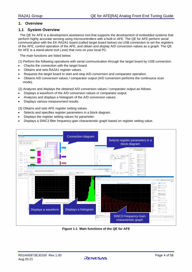
1. Overview
1.1 System Overview
The QE for AFE is a development assistance tool that supports the development of embedded systems that perform highly accurate sensing using microcontrollers with a built-in AFE. The QE for AFE perform serial communication with the EK-RA2A1 board (called target board below) via USB connection to set the registers of the AFE, control operation of the AFE, and obtain and display A/D conversion values as a graph. The QE for AFE is a stand-alone tool (.exe) that runs on your local PC.
The main functions are listed below.
(1) Perform the following operations with serial communication through the target board by USB connection.
• Checks the connection with the target board.
• Obtains and sets RA2A1 register values.
• Requests the target board to start and stop A/D conversion and comparator operation.
• Obtains A/D conversion values / comparator output (A/D conversion performs the continuous scan
mode). (2) Analyzes and displays the obtained A/D conversion values / comparator output as follows.
• Displays a waveform of the A/D conversion values or comparator output.
• Analyzes and displays a histogram of the A/D conversion values.
• Displays various measurement results. (3) Obtains and sets AFE register setting values.
• Selects and specifies register parameters in a block diagram.
• Displays the register setting values for parameter.
• Displays a SINC3 filter frequency-gain characteristic graph based on register setting value.
Figure 1-1 Main functions of the QE for AFE
Connection diagram
Selects register parameters in a
block diagram
Displays a waveform Displays a histogram
SINC3 Frequency-Gain
characteristic graph
RA2A1 Group QE for AFE[RA] Analog Front End Tuning Guide
R01AN5973EJ0100 Rev.1.00 Page 5 of 58
Aug.20.21
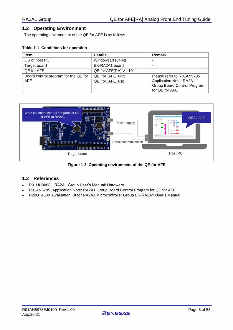
1.2 Operating Environment
The operating environment of the QE for AFE is as follows.
Table 1-1 Conditions for operation
Item Details Remark
OS of host PC Windows10 (64bit) -
Target board EK-RA2A1 board -
QE for AFE QE for AFE[RA] V1.10 -
Board control program for the QE for
AFE
QE_for_AFE_uart
QE_for_AFE_usb
Please refer to R01AN5795
Application Note: RA2A1
Group Board Control Program
for QE for AFE
Figure 1-2 Operating environment of the QE for AFE
1.3 References
• R01UH0888 RA2A1 Group User’s Manual: Hardware
• R01AN5795 Application Note: RA2A1 Group Board Control Program for QE for AFE
• R20UT4580 Evaluation Kit for RA2A1 Microcontroller Group EK-RA2A1 User’s Manual
2
Host PC
Write the board control program for QE
for AFE to RA2A1
Target board
Power supply
Serial communication
QE for AFE
RA2A1 Group QE for AFE[RA] Analog Front End Tuning Guide
R01AN5973EJ0100 Rev.1.00 Page 6 of 58
Aug.20.21
2. Preparation
The necessary preparations to use the QE for AFE are as follows.
• Installation of the QE for AFE
• Programming of the board control program for the QE for AFE
• Settings of the target board
2.1 Installation of the QE for AFE
The QE for AFE is provided in a zip package. The procedure how to use the QE for AFE is as follows.
(1) Unzip the zip file anywhere on your PC.
Unzip the zip file in a shallow folder hierarchy.
Note: Do not place it under the OS program folder (C:\Program Files).
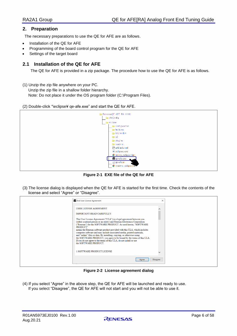
(2) Double-click “\eclipse¥ qe-afe.exe” and start the QE for AFE.
Figure 2-1 EXE file of the QE for AFE
(3) The license dialog is displayed when the QE for AFE is started for the first time. Check the contents of the
license and select “Agree” or “Disagree”.
Figure 2-2 License agreement dialog
(4) If you select “Agree” in the above step, the QE for AFE will be launched and ready to use.
If you select “Disagree”, the QE for AFE will not start and you will not be able to use it.
RA2A1 Group QE for AFE[RA] Analog Front End Tuning Guide
R01AN5973EJ0100 Rev.1.00 Page 7 of 58
Aug.20.21
2.1.1 Update of the QE for AFE
If you want to update the QE for AFE, you can update using the same procedure as installation.
2.1.2 Uninstall of the QE for AFE
If you want to uninstall the QE for AFE, delete the folder where you unzipped the zip file.
2.2 Programming of the board control program for the QE for AFE
For the method of programming the board control program to RA2A1 on the target board, please refer to the application note: “RA2A1 Group Board Control Program for the QE for AFE”.
2.3 Settings of the target board
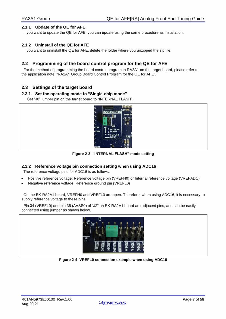
2.3.1 Set the operating mode to “Single-chip mode”
Set “J8” jumper pin on the target board to “INTERNAL FLASH”.
Figure 2-3 “INTERNAL FLASH” mode setting
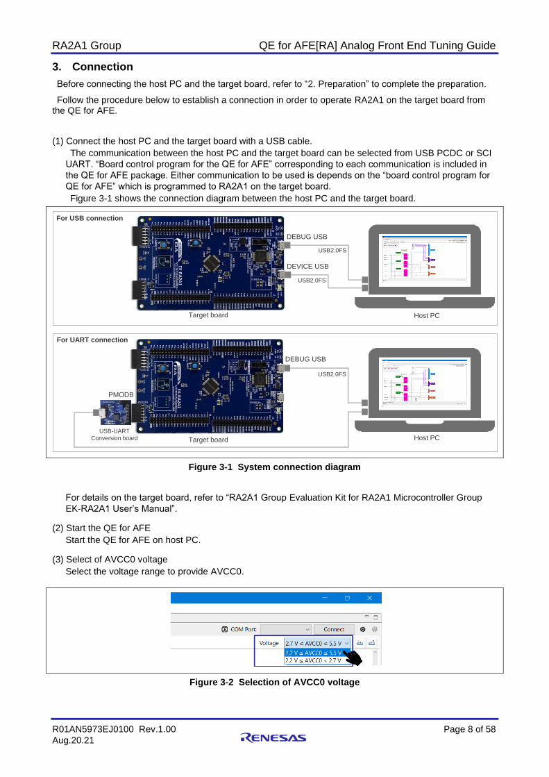
2.3.2 Reference voltage pin connection setting when using ADC16
The reference voltage pins for ADC16 is as follows.
• Positive reference voltage: Reference voltage pin (VREFH0) or Internal reference voltage (VREFADC)
• Negative reference voltage: Reference ground pin (VREFL0)
On the EK-RA2A1 board, VREFH0 and VREFL0 are open. Therefore, when using ADC16, it is necessary to supply reference voltage to these pins.
Pin 34 (VREFL0) and pin 36 (AVSS0) of “J2” on EK-RA2A1 board are adjacent pins, and can be easily connected using jumper as shown below.
Figure 2-4 VREFL0 connection example when using ADC16
RA2A1 Group QE for AFE[RA] Analog Front End Tuning Guide
R01AN5973EJ0100 Rev.1.00 Page 8 of 58
Aug.20.21
3. Connection
Before connecting the host PC and the target board, refer to “2. Preparation” to complete the preparation.
Follow the procedure below to establish a connection in order to operate RA2A1 on the target board from the QE for AFE.
(1) Connect the host PC and the target board with a USB cable.
The communication between the host PC and the target board can be selected from USB PCDC or SCI
UART. “Board control program for the QE for AFE” corresponding to each communication is included in
the QE for AFE package. Either communication to be used is depends on the “board control program for
QE for AFE” which is programmed to RA2A1 on the target board.
Figure 3-1 shows the connection diagram between the host PC and the target board.
Figure 3-1 System connection diagram
For details on the target board, refer to “RA2A1 Group Evaluation Kit for RA2A1 Microcontroller Group
EK-RA2A1 User’s Manual”. (2) Start the QE for AFE
Start the QE for AFE on host PC. (3) Select of AVCC0 voltage
Select the voltage range to provide AVCC0.
Figure 3-2 Selection of AVCC0 voltage
For USB connection
1
DEBUG USB
DEVICE USB
USB2.0FS
Target board
USB2.0FS
Host PC
For UART connection
PMODB
USB-UART
Conversion board
DEBUG USB
USB2.0FS
Target board Host PC
RA2A1 Group QE for AFE[RA] Analog Front End Tuning Guide
R01AN5973EJ0100 Rev.1.00 Page 9 of 58
Aug.20.21
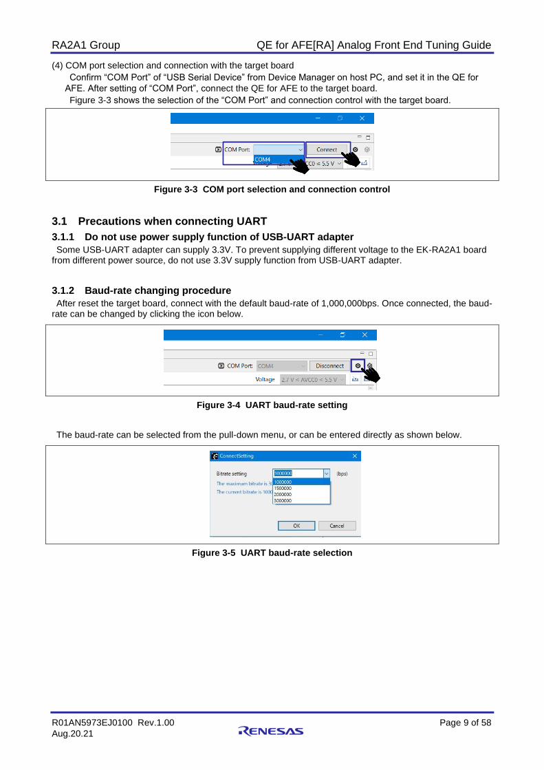
(4) COM port selection and connection with the target board
Confirm “COM Port” of “USB Serial Device” from Device Manager on host PC, and set it in the QE for
AFE. After setting of “COM Port”, connect the QE for AFE to the target board.
Figure 3-3 shows the selection of the “COM Port” and connection control with the target board.
Figure 3-3 COM port selection and connection control
3.1 Precautions when connecting UART
3.1.1 Do not use power supply function of USB-UART adapter
Some USB-UART adapter can supply 3.3V. To prevent supplying different voltage to the EK-RA2A1 board from different power source, do not use 3.3V supply function from USB-UART adapter.
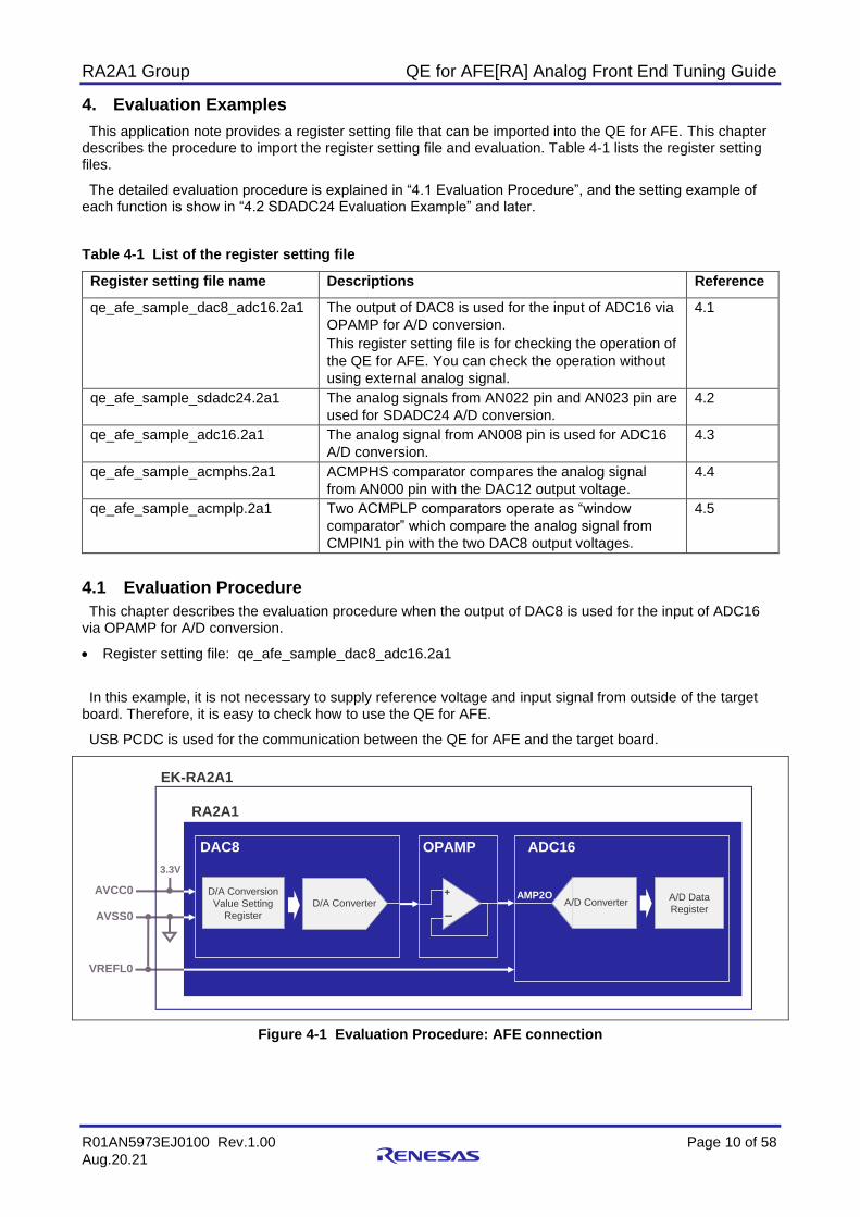
3.1.2 Baud-rate changing procedure
After reset the target board, connect with the default baud-rate of 1,000,000bps. Once connected, the baud-rate can be changed by clicking the icon below.
Figure 3-4 UART baud-rate setting
The baud-rate can be selected from the pull-down menu, or can be entered directly as shown below.
Figure 3-5 UART baud-rate selection
RA2A1 Group QE for AFE[RA] Analog Front End Tuning Guide
R01AN5973EJ0100 Rev.1.00 Page 10 of 58
Aug.20.21
4. Evaluation Examples
This application note provides a register setting file that can be imported into the QE for AFE. This chapter describes the procedure to import the register setting file and evaluation. Table 4-1 lists the register setting files.
The detailed evaluation procedure is explained in “4.1 Evaluation Procedure”, and the setting example of each function is show in “4.2 SDADC24 Evaluation Example” and later.
Table 4-1 List of the register setting file
Register setting file name Descriptions Reference
qe_afe_sample_dac8_adc16.2a1 The output of DAC8 is used for the input of ADC16 via
OPAMP for A/D conversion.
This register setting file is for checking the operation of
the QE for AFE. You can check the operation without
using external analog signal.
4.1
qe_afe_sample_sdadc24.2a1 The analog signals from AN022 pin and AN023 pin are
used for SDADC24 A/D conversion.
4.2
qe_afe_sample_adc16.2a1 The analog signal from AN008 pin is used for ADC16
A/D conversion.
4.3
qe_afe_sample_acmphs.2a1 ACMPHS comparator compares the analog signal
from AN000 pin with the DAC12 output voltage.
4.4
qe_afe_sample_acmplp.2a1 Two ACMPLP comparators operate as “window
comparator” which compare the analog signal from
CMPIN1 pin with the two DAC8 output voltages.
4.5
4.1 Evaluation Procedure
This chapter describes the evaluation procedure when the output of DAC8 is used for the input of ADC16 via OPAMP for A/D conversion.
• Register setting file: qe_afe_sample_dac8_adc16.2a1
In this example, it is not necessary to supply reference voltage and input signal from outside of the target board. Therefore, it is easy to check how to use the QE for AFE.
USB PCDC is used for the communication between the QE for AFE and the target board.
Figure 4-1 Evaluation Procedure: AFE connection
ADC16
A/D Data
Register
RA2A1
VREFL0
DAC8
D/A Conversion
Value Setting
Register
AVCC0
AVSS0
+
ー
OPAMP
AMP2O
3.3V
EK-RA2A1
D/A Converter A/D Converter
RA2A1 Group QE for AFE[RA] Analog Front End Tuning Guide
R01AN5973EJ0100 Rev.1.00 Page 11 of 58
Aug.20.21
4.1.1 Preparation
Follow “2 Preparation” to prepare for using the QE for AFE.
• Installation of the QE for AFE
• Programming of the board control program for the QE for AFE
• Settings of the target board
⎯ Set “J8” jumper pin on the target board to “INTERNAL FLASH”.
⎯ Short “VREFL0” pin and “AVSS0” pin to use ADC16.
4.1.2 Connect host PC to the target board
Connect host PC and the target board as shown below.
Figure 4-2 Evaluation Procedure: Connect host PC and the target board
4.1.3 Connect the QE for AFE and the target board
Start the QE for AFE.
3.3V is supplied to AVCC0 of the target board. Select the voltage range to provide AVCC0 as shown below.
Figure 4-3 Evaluation Procedure: Selection of AVCC0 voltage
Select “COM Port”, and click “Connect”.
Figure 4-4 Evaluation Procedure: COM port selection and connection control
2
DEBUG USB
DEVICE USB
USB2.0FS
Target board EK-RA2A1
USB2.0FS
Host PC
RA2A1 Group QE for AFE[RA] Analog Front End Tuning Guide
R01AN5973EJ0100 Rev.1.00 Page 12 of 58
Aug.20.21
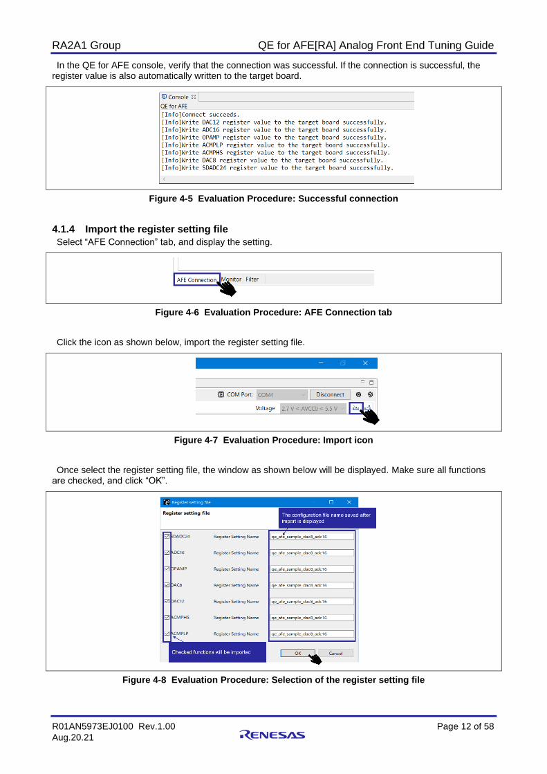
In the QE for AFE console, verify that the connection was successful. If the connection is successful, the register value is also automatically written to the target board.
Figure 4-5 Evaluation Procedure: Successful connection
4.1.4 Import the register setting file
Select “AFE Connection” tab, and display the setting.
Figure 4-6 Evaluation Procedure: AFE Connection tab
Click the icon as shown below, import the register setting file.
Figure 4-7 Evaluation Procedure: Import icon
Once select the register setting file, the window as shown below will be displayed. Make sure all functions are checked, and click “OK”.
Figure 4-8 Evaluation Procedure: Selection of the register setting file

RA2A1 Group QE for AFE[RA] Analog Front End Tuning Guide
R01AN5973EJ0100 Rev.1.00 Page 13 of 58
Aug.20.21
4.1.5 Configuration of DAC8
In the register setting file, DAC8 Channel1 is used to perform D/A conversion of 0x73 to generate an analog signal (about 1.5V).
Select “DAC8” tab, and display the setting.
Figure 4-9 Evaluation Procedure; DAC8 tab
DAC8 is configured as shown below.
Figure 4-10 Evaluation Procedure: Configuration of DAC8
Enable DAC8 ch1
Set D/A conversion value
RA2A1 Group QE for AFE[RA] Analog Front End Tuning Guide
R01AN5973EJ0100 Rev.1.00 Page 14 of 58
Aug.20.21
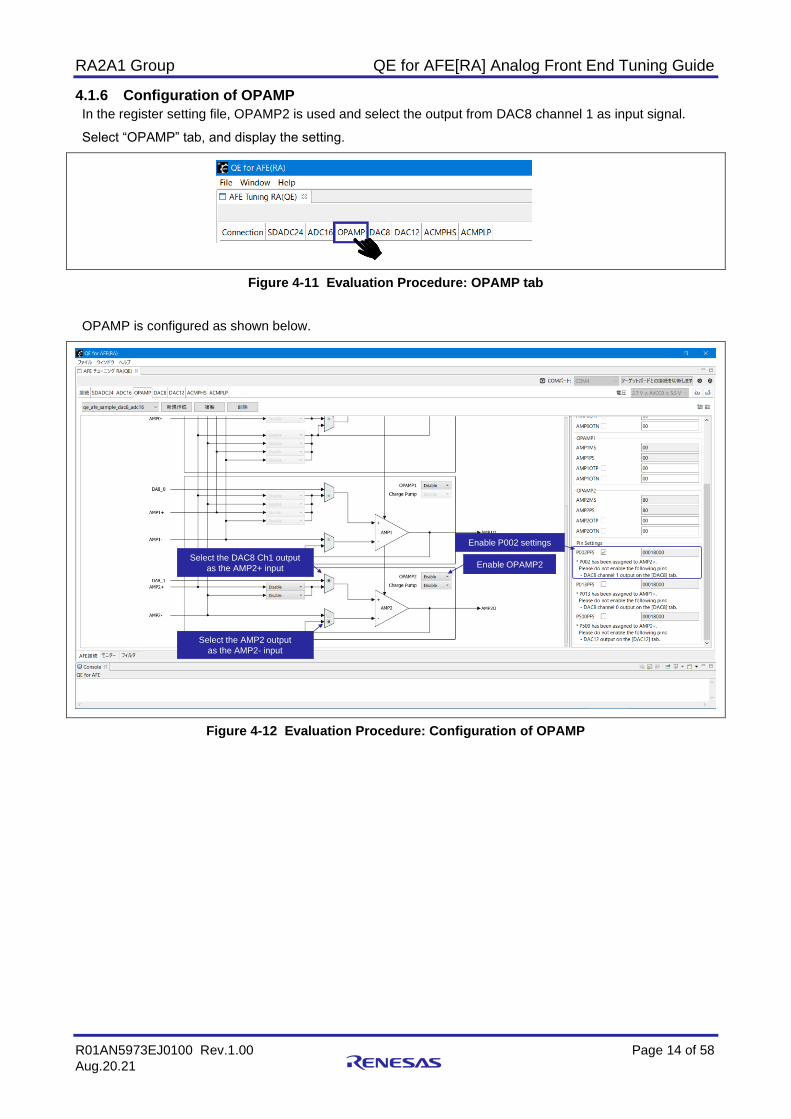
4.1.6 Configuration of OPAMP
In the register setting file, OPAMP2 is used and select the output from DAC8 channel 1 as input signal.
Select “OPAMP” tab, and display the setting.
Figure 4-11 Evaluation Procedure: OPAMP tab
OPAMP is configured as shown below.
Figure 4-12 Evaluation Procedure: Configuration of OPAMP
Select the DAC8 Ch1 output
as the AMP2+ input
Select the AMP2 output
as the AMP2- input
Enable OPAMP2
Enable P002 settings
RA2A1 Group QE for AFE[RA] Analog Front End Tuning Guide
R01AN5973EJ0100 Rev.1.00 Page 15 of 58
Aug.20.21
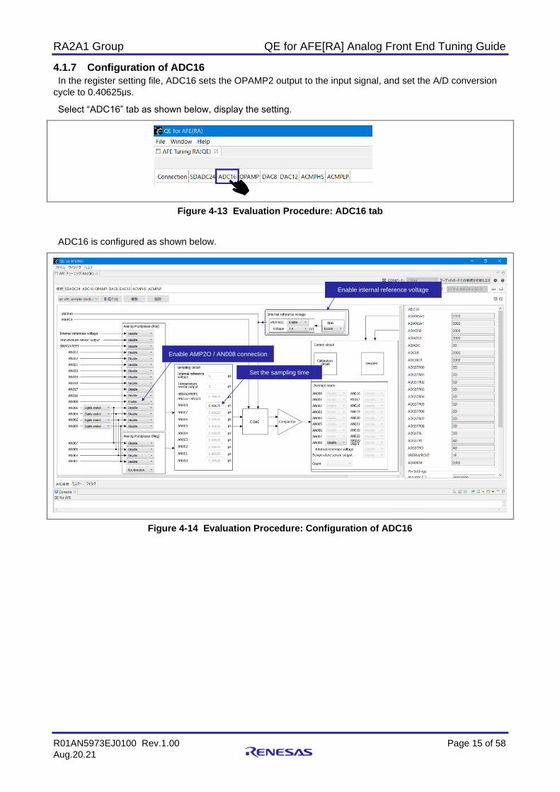
4.1.7 Configuration of ADC16
In the register setting file, ADC16 sets the OPAMP2 output to the input signal, and set the A/D conversion
cycle to 0.40625µs.
Select “ADC16” tab as shown below, display the setting.
Figure 4-13 Evaluation Procedure: ADC16 tab
ADC16 is configured as shown below.
Figure 4-14 Evaluation Procedure: Configuration of ADC16
Enable AMP2O / AN008 connection
Set the sampling time
Enable internal reference voltage
RA2A1 Group QE for AFE[RA] Analog Front End Tuning Guide
R01AN5973EJ0100 Rev.1.00 Page 16 of 58
Aug.20.21
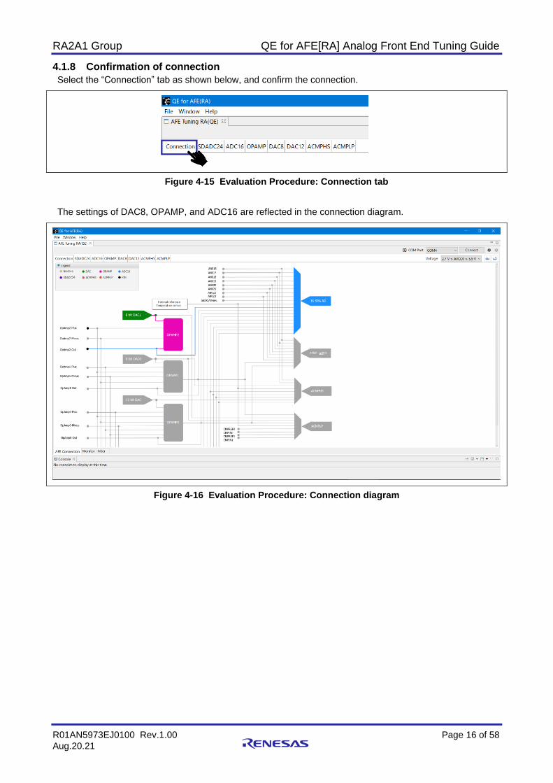
4.1.8 Confirmation of connection
Select the “Connection” tab as shown below, and confirm the connection.
Figure 4-15 Evaluation Procedure: Connection tab
The settings of DAC8, OPAMP, and ADC16 are reflected in the connection diagram.
Figure 4-16 Evaluation Procedure: Connection diagram
RA2A1 Group QE for AFE[RA] Analog Front End Tuning Guide
R01AN5973EJ0100 Rev.1.00 Page 17 of 58
Aug.20.21
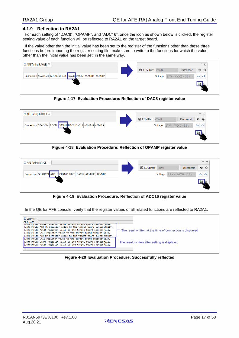
4.1.9 Reflection to RA2A1
For each setting of “DAC8”, “OPAMP”, and “ADC16”, once the icon as shown below is clicked, the register setting value of each function will be reflected to RA2A1 on the target board.
If the value other than the initial value has been set to the register of the functions other than these three functions before importing the register setting file, make sure to write to the functions for which the value other than the initial value has been set, in the same way.
Figure 4-17 Evaluation Procedure: Reflection of DAC8 register value
Figure 4-18 Evaluation Procedure: Reflection of OPAMP register value
Figure 4-19 Evaluation Procedure: Reflection of ADC16 register value
In the QE for AFE console, verify that the register values of all related functions are reflected to RA2A1.
Figure 4-20 Evaluation Procedure: Successfully reflected
The result written at the time of connection is displayed
The result written after setting is displayed
RA2A1 Group QE for AFE[RA] Analog Front End Tuning Guide
R01AN5973EJ0100 Rev.1.00 Page 18 of 58
Aug.20.21
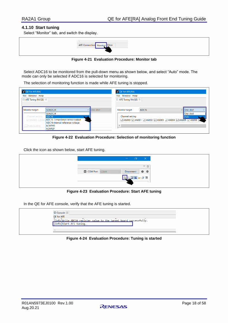
4.1.10 Start tuning
Select “Monitor” tab, and switch the display.
Figure 4-21 Evaluation Procedure: Monitor tab
Select ADC16 to be monitored from the pull-down menu as shown below, and select “Auto” mode. The mode can only be selected if ADC16 is selected for monitoring.
The selection of monitoring function is made while AFE tuning is stopped.
Figure 4-22 Evaluation Procedure: Selection of monitoring function
Click the icon as shown below, start AFE tuning.
Figure 4-23 Evaluation Procedure: Start AFE tuning
In the QE for AFE console, verify that the AFE tuning is started.
Figure 4-24 Evaluation Procedure: Tuning is started
RA2A1 Group QE for AFE[RA] Analog Front End Tuning Guide
R01AN5973EJ0100 Rev.1.00 Page 19 of 58
Aug.20.21
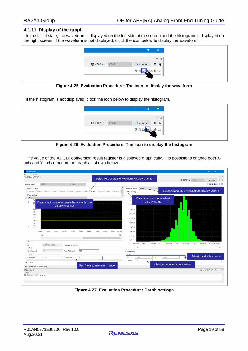
4.1.11 Display of the graph
In the initial state, the waveform is displayed on the left side of the screen and the histogram is displayed on the right screen. If the waveform is not displayed, clock the icon below to display the waveform.
Figure 4-25 Evaluation Procedure: The icon to display the waveform
If the histogram is not displayed, clock the icon below to display the histogram.
Figure 4-26 Evaluation Procedure: The icon to display the histogram
The value of the ADC16 conversion result register is displayed graphically. It is possible to change both X-axis and Y-axis range of the graph as shown below.
Figure 4-27 Evaluation Procedure: Graph settings
Select AN008 as the waveform display channel
Select AN008 as the histogram display channel
Disable auto scale because there is only one
display channel
Set Y axis to maximum range Change the number of classes
Disable auto scale to adjust
display range
Adjust the display range
RA2A1 Group QE for AFE[RA] Analog Front End Tuning Guide
R01AN5973EJ0100 Rev.1.00 Page 20 of 58
Aug.20.21
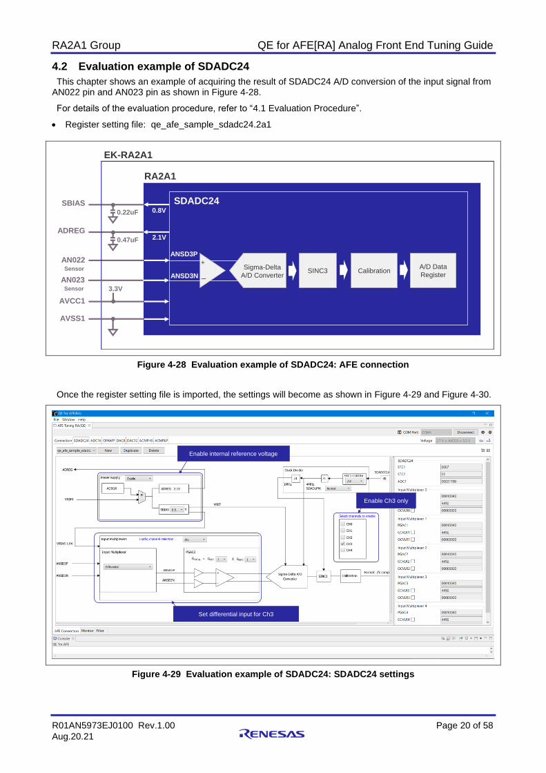
4.2 Evaluation example of SDADC24
This chapter shows an example of acquiring the result of SDADC24 A/D conversion of the input signal from AN022 pin and AN023 pin as shown in Figure 4-28.
For details of the evaluation procedure, refer to “4.1 Evaluation Procedure”.
• Register setting file: qe_afe_sample_sdadc24.2a1
Figure 4-28 Evaluation example of SDADC24: AFE connection
Once the register setting file is imported, the settings will become as shown in Figure 4-29 and Figure 4-30.
Figure 4-29 Evaluation example of SDADC24: SDADC24 settings
AN022
SINC3 Calibration
SDADC24SBIAS
+
ー
A/D Data
Register
ADREG
RA2A1
ANSD3P
Sensor
EK-RA2A1
0.22uF
0.47uF
0.8V
2.1V
Sigma-Delta
A/D Converter
AVCC1
AVSS1
3.3V
AN023Sensor
ANSD3N
Enable internal reference voltage
Set differential input for Ch3
Enable Ch3 only
RA2A1 Group QE for AFE[RA] Analog Front End Tuning Guide
R01AN5973EJ0100 Rev.1.00 Page 21 of 58
Aug.20.21
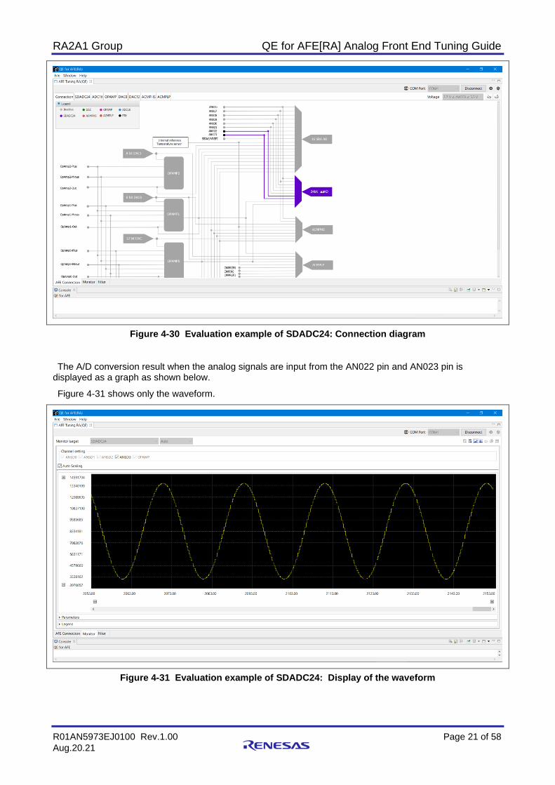
Figure 4-30 Evaluation example of SDADC24: Connection diagram
The A/D conversion result when the analog signals are input from the AN022 pin and AN023 pin is displayed as a graph as shown below.
Figure 4-31 shows only the waveform.
Figure 4-31 Evaluation example of SDADC24: Display of the waveform

RA2A1 Group QE for AFE[RA] Analog Front End Tuning Guide
R01AN5973EJ0100 Rev.1.00 Page 22 of 58
Aug.20.21
4.3 Evaluation example of ADC16
This chapter shows an example of acquiring the result of ADC16 A/D conversion of the input signal from AN008 pin as shown in Figure 4-32.
For details of the evaluation procedure, refer to “4.1 Evaluation Procedure”.
• Register setting file: qe_afe_sample_adc16.2a1
Figure 4-32 Evaluation example of ADC16: AFE connection
Once the register setting file is imported, the settings will become as shown in Figure 4-33 and Figure 4-34.
Figure 4-33 Evaluation example of ADC16: ADC16 settings
AN008
ADC16
A/D Data
Register
RA2A1
VREFL0
Sensor
EK-RA2A1
AVSS0
A/D Converter
Enable internal reference voltage
Enable AN008 connection
Set the sampling period
RA2A1 Group QE for AFE[RA] Analog Front End Tuning Guide
R01AN5973EJ0100 Rev.1.00 Page 23 of 58
Aug.20.21
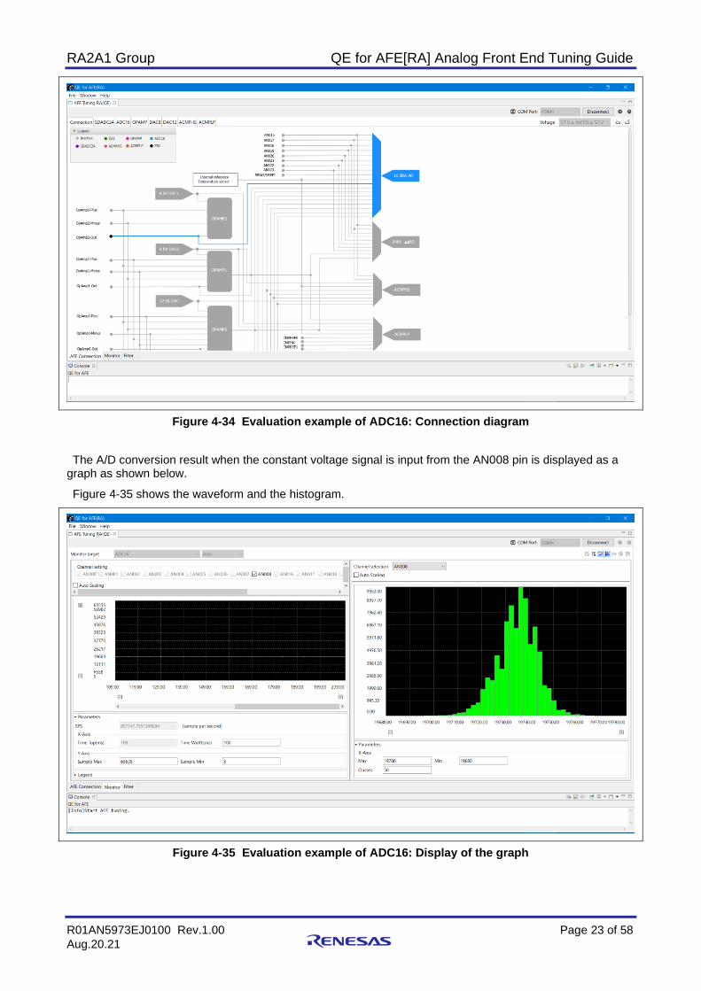
Figure 4-34 Evaluation example of ADC16: Connection diagram
The A/D conversion result when the constant voltage signal is input from the AN008 pin is displayed as a graph as shown below.
Figure 4-35 shows the waveform and the histogram.
Figure 4-35 Evaluation example of ADC16: Display of the graph
RA2A1 Group QE for AFE[RA] Analog Front End Tuning Guide
R01AN5973EJ0100 Rev.1.00 Page 24 of 58
Aug.20.21
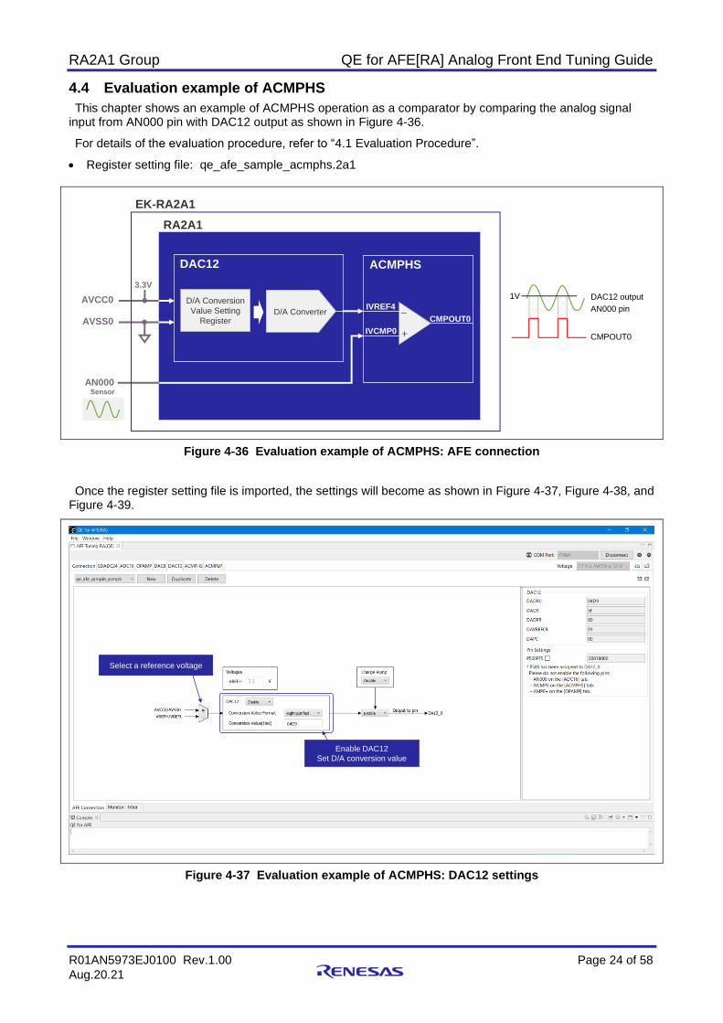
4.4 Evaluation example of ACMPHS
This chapter shows an example of ACMPHS operation as a comparator by comparing the analog signal input from AN000 pin with DAC12 output as shown in Figure 4-36.
For details of the evaluation procedure, refer to “4.1 Evaluation Procedure”.
• Register setting file: qe_afe_sample_acmphs.2a1
Figure 4-36 Evaluation example of ACMPHS: AFE connection
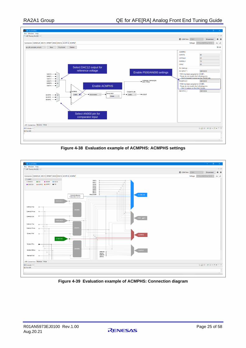
Once the register setting file is imported, the settings will become as shown in Figure 4-37, Figure 4-38, and Figure 4-39.
Figure 4-37 Evaluation example of ACMPHS: DAC12 settings
CMPOUT0
DAC12 output
AN000 pin
AN000
ACMPHS
ー
+
RA2A1
DAC12
D/A Conversion
Value Setting
Register
AVCC0
AVSS0
IVREF4
IVCMP0
CMPOUT0
Sensor
EK-RA2A1
3.3V
D/A Converter
1V
Select a reference voltage
Enable DAC12
Set D/A conversion value
RA2A1 Group QE for AFE[RA] Analog Front End Tuning Guide
R01AN5973EJ0100 Rev.1.00 Page 25 of 58
Aug.20.21
Figure 4-38 Evaluation example of ACMPHS: ACMPHS settings
Figure 4-39 Evaluation example of ACMPHS: Connection diagram
Select DAC12 output for
reference voltage
Select AN000 pin for
comparator input
Enable ACMPHS
Enable P500/AN000 settings
RA2A1 Group QE for AFE[RA] Analog Front End Tuning Guide
R01AN5973EJ0100 Rev.1.00 Page 26 of 58
Aug.20.21
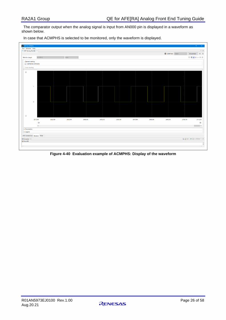
The comparator output when the analog signal is input from AN000 pin is displayed in a waveform as shown below.
In case that ACMPHS is selected to be monitored, only the waveform is displayed.
Figure 4-40 Evaluation example of ACMPHS: Display of the waveform
RA2A1 Group QE for AFE[RA] Analog Front End Tuning Guide
R01AN5973EJ0100 Rev.1.00 Page 27 of 58
Aug.20.21
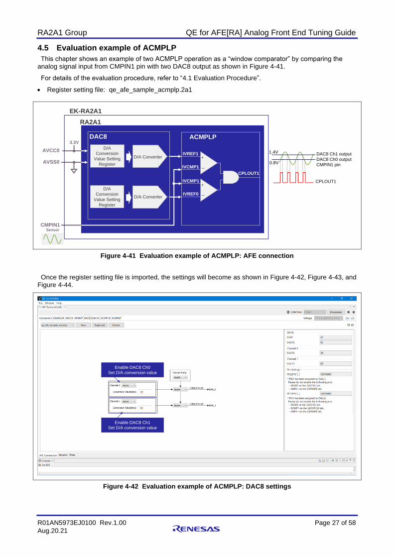
4.5 Evaluation example of ACMPLP
This chapter shows an example of two ACMPLP operation as a “window comparator” by comparing the analog signal input from CMPIN1 pin with two DAC8 output as shown in Figure 4-41.
For details of the evaluation procedure, refer to “4.1 Evaluation Procedure”.
• Register setting file: qe_afe_sample_acmplp.2a1
Figure 4-41 Evaluation example of ACMPLP: AFE connection
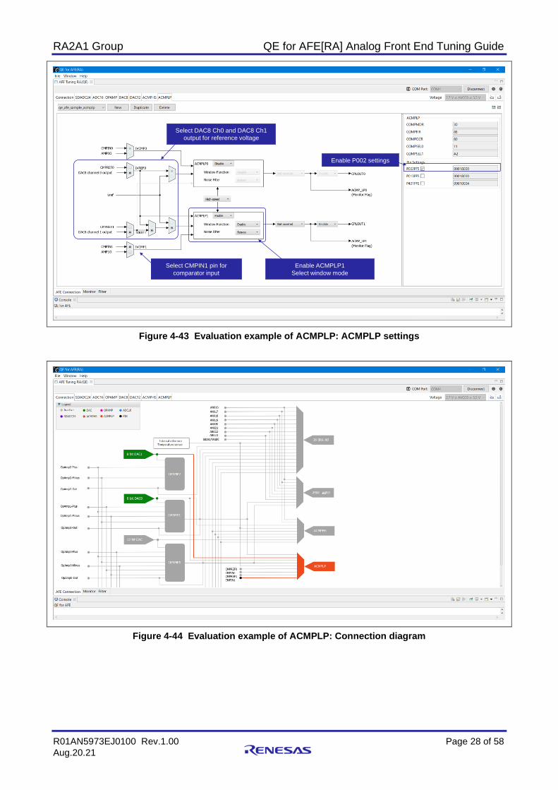
Once the register setting file is imported, the settings will become as shown in Figure 4-42, Figure 4-43, and Figure 4-44.
Figure 4-42 Evaluation example of ACMPLP: DAC8 settings
CMPIN1
ACMPLP
+
ー
RA2A1
DAC8
D/A
Conversion
Value Setting
Register
AVCC0
AVSS0
D/A
Conversion
Value Setting
Register
+
ー
IVREF1
IVCMP1
IVREF0
IVCMP1
CPLOUT1
CPLOUT1
DAC8 Ch1 output
DAC8 Ch0 output
CMPIN1 pin
Sensor
EK-RA2A1
3.3V
D/A Converter
D/A Converter1.4V
0.8V
Enable DAC8 Ch1
Set D/A conversion value
Enable DAC8 Ch0
Set D/A conversion value
RA2A1 Group QE for AFE[RA] Analog Front End Tuning Guide
R01AN5973EJ0100 Rev.1.00 Page 28 of 58
Aug.20.21
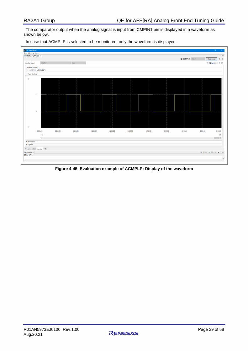
Figure 4-43 Evaluation example of ACMPLP: ACMPLP settings
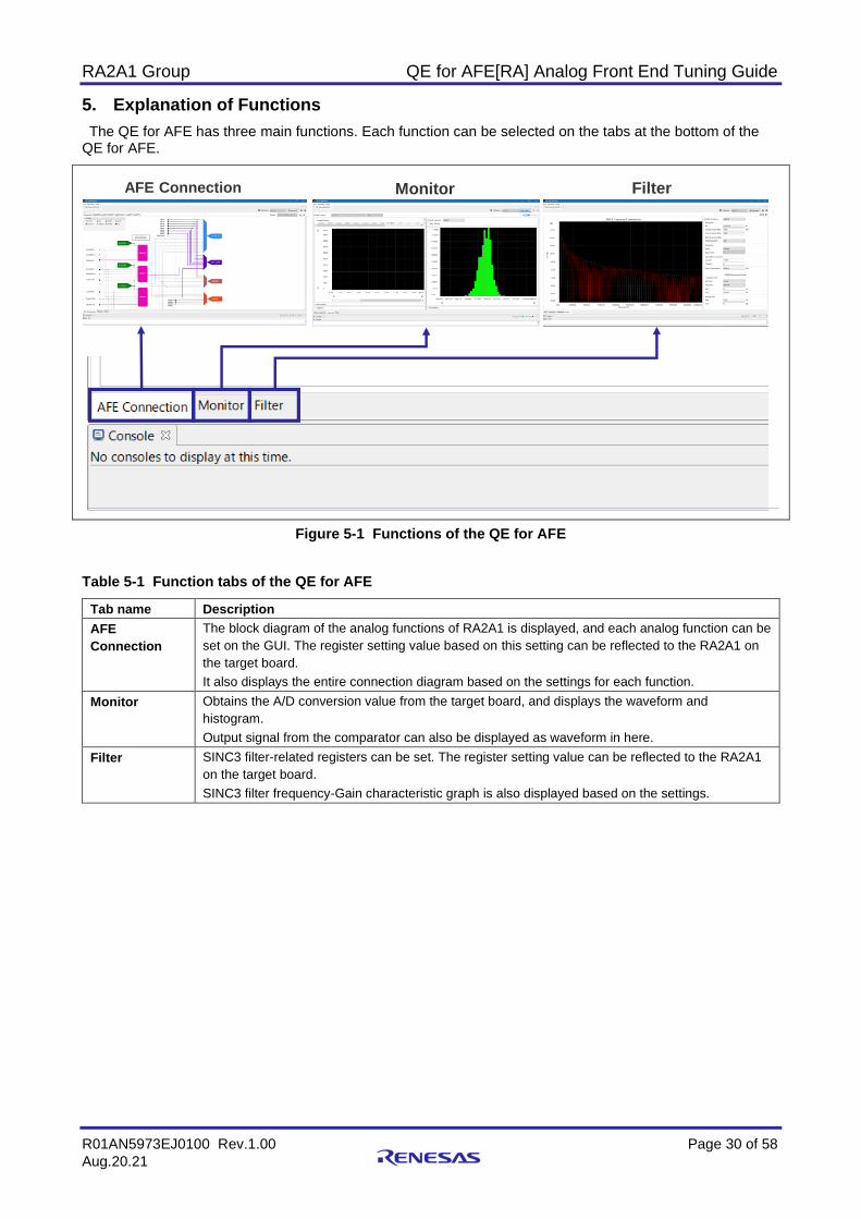
Figure 4-44 Evaluation example of ACMPLP: Connection diagram
Select DAC8 Ch0 and DAC8 Ch1
output for reference voltage
Select CMPIN1 pin for
comparator input
Enable ACMPLP1
Select window mode
Enable P002 settings
RA2A1 Group QE for AFE[RA] Analog Front End Tuning Guide
R01AN5973EJ0100 Rev.1.00 Page 29 of 58
Aug.20.21
The comparator output when the analog signal is input from CMPIN1 pin is displayed in a waveform as shown below.
In case that ACMPLP is selected to be monitored, only the waveform is displayed.
Figure 4-45 Evaluation example of ACMPLP: Display of the waveform
RA2A1 Group QE for AFE[RA] Analog Front End Tuning Guide
R01AN5973EJ0100 Rev.1.00 Page 30 of 58
Aug.20.21
5. Explanation of Functions
The QE for AFE has three main functions. Each function can be selected on the tabs at the bottom of the QE for AFE.
Figure 5-1 Functions of the QE for AFE
Table 5-1 Function tabs of the QE for AFE
Tab name Description
AFE
Connection
The block diagram of the analog functions of RA2A1 is displayed, and each analog function can be
set on the GUI. The register setting value based on this setting can be reflected to the RA2A1 on
the target board.
It also displays the entire connection diagram based on the settings for each function.
Monitor Obtains the A/D conversion value from the target board, and displays the waveform and
histogram.
Output signal from the comparator can also be displayed as waveform in here.
Filter SINC3 filter-related registers can be set. The register setting value can be reflected to the RA2A1
on the target board.
SINC3 filter frequency-Gain characteristic graph is also displayed based on the settings.
Monitor FilterAFE Connection
RA2A1 Group QE for AFE[RA] Analog Front End Tuning Guide
R01AN5973EJ0100 Rev.1.00 Page 31 of 58
Aug.20.21
5.1 AFE Connection
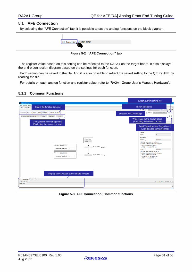
By selecting the “AFE Connection” tab, it is possible to set the analog functions on the block diagram.
Figure 5-2 “AFE Connection” tab
The register value based on this setting can be reflected to the RA2A1 on the target board. It also displays the entire connection diagram based on the settings for each function.
Each setting can be saved to the file. And it is also possible to reflect the saved setting to the QE for AFE by reading the file.
For details on each analog function and register value, refer to “RA2A1 Group User’s Manual: Hardware”.
5.1.1 Common Functions
Figure 5-3 AFE Connection: Common functions
Select the function to be set
Configuration file management
(Excluding the connection tab)
Display the execution status on the console
Export current setting file
Import setting file
Select of AVCC0 voltage
Write Value to the Target Board
(Excluding the connection tab)
Read Value from the Target Board
(Excluding the connection tab)
RA2A1 Group QE for AFE[RA] Analog Front End Tuning Guide
R01AN5973EJ0100 Rev.1.00 Page 32 of 58
Aug.20.21
• Selecting of function to be set
The analog function to be set can be selected from the tabs. For details of each tab will be explained in
the following chapters.
Figure 5-4 AFE Connection: Selecting of function to be set
• Selecting of AVCC0 voltage
The AVCC0 voltage to be supplied to the target board can be selected from the pull-down menu as
shown below. It cannot be changed while connecting the QE for AFE and the target board.
Figure 5-5 AFE Connection: Selecting of AVCC0 voltage
RA2A1 Group QE for AFE[RA] Analog Front End Tuning Guide
R01AN5973EJ0100 Rev.1.00 Page 33 of 58
Aug.20.21
Table 5-2 AFE Connection: Common functions
Icon Description Condition
Before
connection
After
connection Note
Stop Running
Import the register settings from the file, and reflect to the QE
for AFE. The function to be imported is selectable. The
extension of the import file is “.2a1”, and the file can be saved
to any location.
✓ ✓
Export the register settings of the QE for AFE to the file.
The function to be exported is selectable. The extension of the
export file is “.2a1”, and the file can be saved to any location
✓ ✓
Reflect the register value of the QE for AFE to RA2A1.
This operation will be done only for the function which is selected.
✓
Reflect the register value of RA2A1 to the QE for AFE.
This operation will be done only for the function which is selected.
✓
The currently selected configuration file name is displayed.
It is also possible to change to another configuration file from the
pull-down menu. In case to change the configuration file, the
configuration file before the change will be automatically saved.
The configuration file is saved by each function in the “afeConfig”
folder in the folder where the QE for AFE is unzipped. The import
operation will be done for multiple functions, while this
configuration file operation will be done only for the selected
function. The extension of the configuration file is “.cn”.
✓ ✓ ✓
The register settings of the QE for AFE will be reset to the
initial value of RA2A1, and create another configuration file
with a different name.
The register settings before this operation will be automatically
saved in the configuration file.
✓ ✓ ✓
The configuration file will be duplicated with a different name. ✓ ✓ ✓
The selected configuration file will be deleted. ✓ ✓ ✓
Note. After connecting the QE for AFE and the target board, the condition when AFE tuning is stopped and when
AFE tuning is running is different.
RA2A1 Group QE for AFE[RA] Analog Front End Tuning Guide
R01AN5973EJ0100 Rev.1.00 Page 34 of 58
Aug.20.21
5.1.2 Connection tab
By selecting the “Connection” tab, the entire connection diagram based on each analog function setting is displayed.
Figure 5-6 AFE Connection: Connection tab
You can check the connection status of the analog function on this screen. There are no items to set on this screen.
Figure 5-7 AFE connection diagram
RA2A1 Group QE for AFE[RA] Analog Front End Tuning Guide
R01AN5973EJ0100 Rev.1.00 Page 35 of 58
Aug.20.21
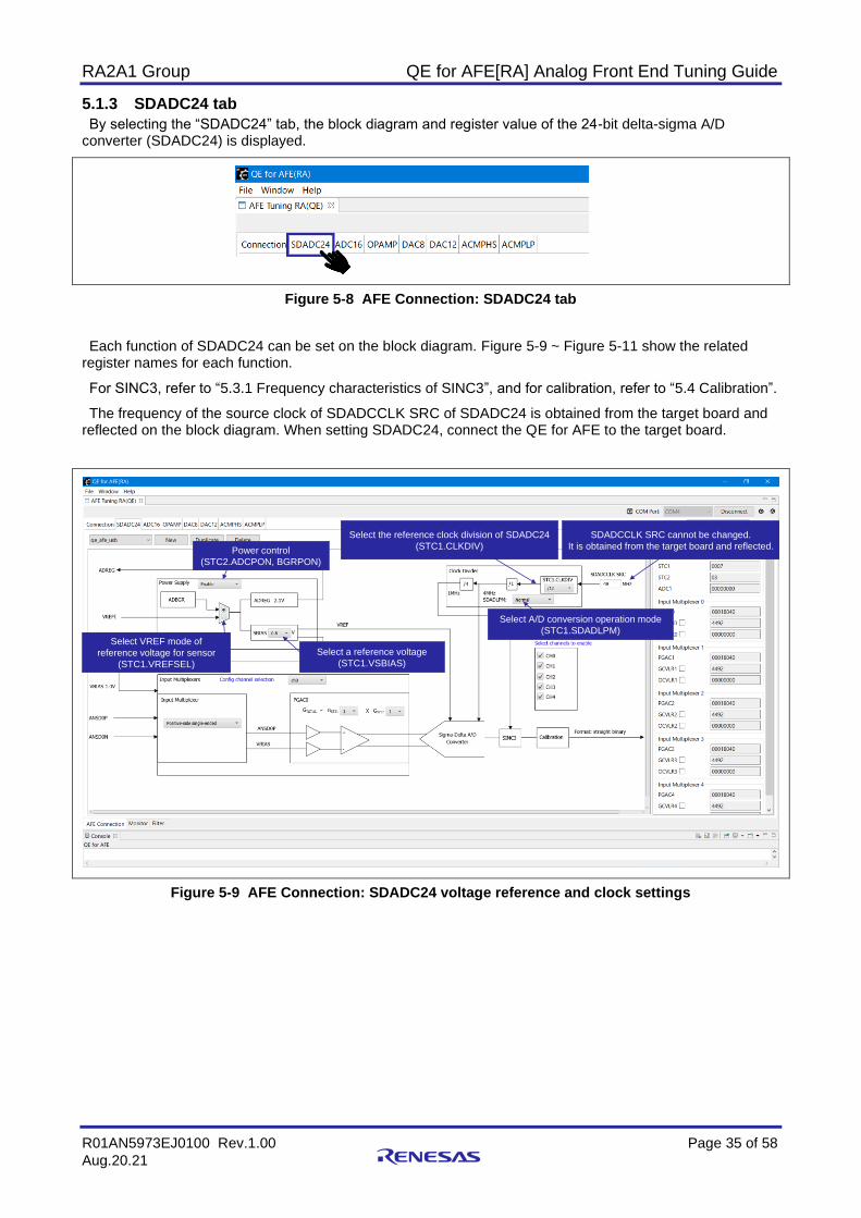
5.1.3 SDADC24 tab
By selecting the “SDADC24” tab, the block diagram and register value of the 24-bit delta-sigma A/D converter (SDADC24) is displayed.
Figure 5-8 AFE Connection: SDADC24 tab
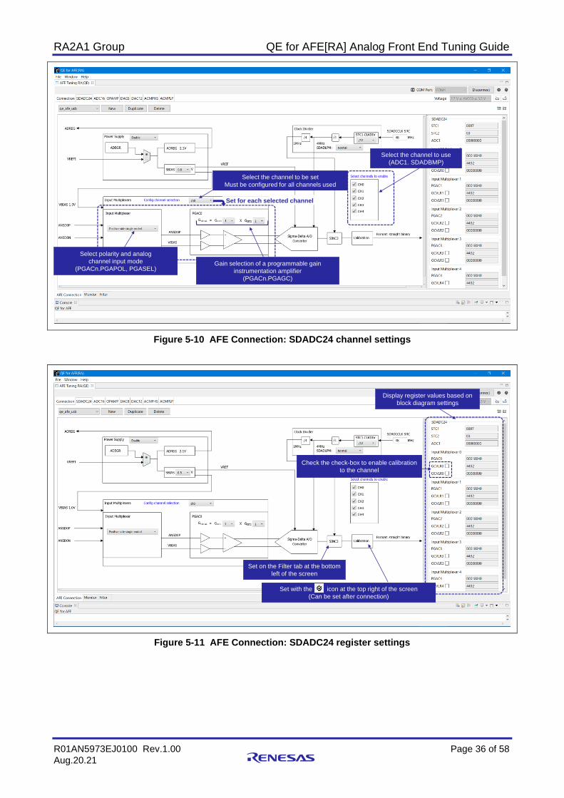
Each function of SDADC24 can be set on the block diagram. Figure 5-9 ~ Figure 5-11 show the related register names for each function.
For SINC3, refer to “5.3.1 Frequency characteristics of SINC3”, and for calibration, refer to “5.4 Calibration”.
The frequency of the source clock of SDADCCLK SRC of SDADC24 is obtained from the target board and reflected on the block diagram. When setting SDADC24, connect the QE for AFE to the target board.
Figure 5-9 AFE Connection: SDADC24 voltage reference and clock settings
Power control
(STC2.ADCPON, BGRPON)
Select VREF mode of
reference voltage for sensor
(STC1.VREFSEL)
Select a reference voltage
(STC1.VSBIAS)
SDADCCLK SRC cannot be changed.
It is obtained from the target board and reflected.
Select the reference clock division of SDADC24
(STC1.CLKDIV)
Select A/D conversion operation mode
(STC1.SDADLPM)
RA2A1 Group QE for AFE[RA] Analog Front End Tuning Guide
R01AN5973EJ0100 Rev.1.00 Page 36 of 58
Aug.20.21
Figure 5-10 AFE Connection: SDADC24 channel settings
Figure 5-11 AFE Connection: SDADC24 register settings
Select the channel to be set
Must be configured for all channels used
Select the channel to use
(ADC1. SDADBMP)
Set for each selected channel
Select polarity and analog
channel input mode
(PGACn.PGAPOL, PGASEL)Gain selection of a programmable gain
instrumentation amplifier
(PGACn.PGAGC)
Set on the Filter tab at the bottom
left of the screen
Set with the A icon at the top right of the screen
(Can be set after connection)
Display register values based on
block diagram settings
Check the check-box to enable calibration
to the channel
RA2A1 Group QE for AFE[RA] Analog Front End Tuning Guide
R01AN5973EJ0100 Rev.1.00 Page 37 of 58
Aug.20.21
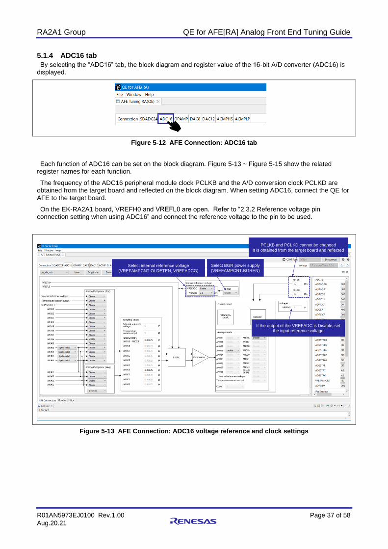
5.1.4 ADC16 tab
By selecting the “ADC16” tab, the block diagram and register value of the 16-bit A/D converter (ADC16) is displayed.
Figure 5-12 AFE Connection: ADC16 tab
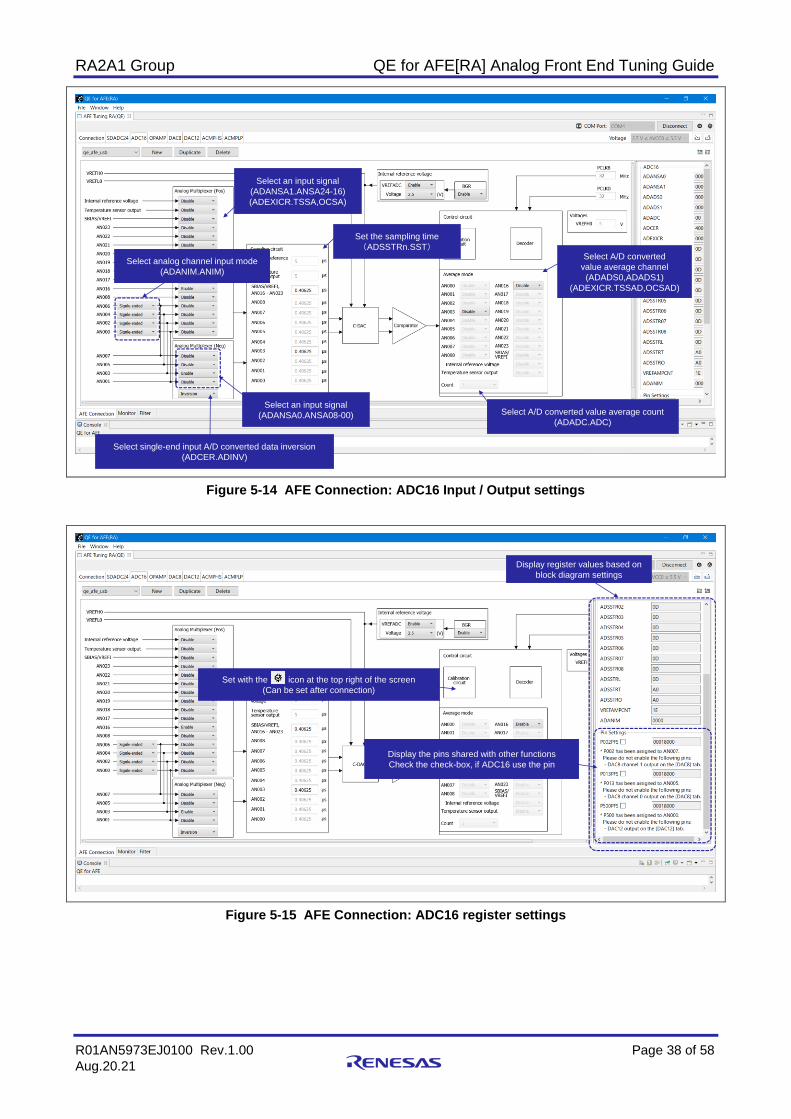
Each function of ADC16 can be set on the block diagram. Figure 5-13 ~ Figure 5-15 show the related register names for each function.
The frequency of the ADC16 peripheral module clock PCLKB and the A/D conversion clock PCLKD are obtained from the target board and reflected on the block diagram. When setting ADC16, connect the QE for AFE to the target board.
On the EK-RA2A1 board, VREFH0 and VREFL0 are open. Refer to “2.3.2 Reference voltage pin connection setting when using ADC16” and connect the reference voltage to the pin to be used.
Figure 5-13 AFE Connection: ADC16 voltage reference and clock settings
Select BGR power supply
(VREFAMPCNT.BGREN)Select internal reference voltage
(VREFAMPCNT.OLDETEN, VREFADCG)
PCLKB and PCLKD cannot be changed
It is obtained from the target board and reflected
If the output of the VREFADC is Disable, set
the input reference voltage
RA2A1 Group QE for AFE[RA] Analog Front End Tuning Guide
R01AN5973EJ0100 Rev.1.00 Page 38 of 58
Aug.20.21
Figure 5-14 AFE Connection: ADC16 Input / Output settings
Figure 5-15 AFE Connection: ADC16 register settings
Select analog channel input mode
(ADANIM.ANIM)
Select an input signal
(ADANSA1.ANSA24-16)
(ADEXICR.TSSA,OCSA)
Select an input signal
(ADANSA0.ANSA08-00)
Select single-end input A/D converted data inversion
(ADCER.ADINV)
Set the sampling time
(ADSSTRn.SST)
Select A/D converted value average count
(ADADC.ADC)
Select A/D converted
value average channel
(ADADS0,ADADS1)
(ADEXICR.TSSAD,OCSAD)
Set with the A icon at the top right of the screen
(Can be set after connection)
Display register values based on
block diagram settings
Display the pins shared with other functions
Check the check-box, if ADC16 use the pin
RA2A1 Group QE for AFE[RA] Analog Front End Tuning Guide
R01AN5973EJ0100 Rev.1.00 Page 39 of 58
Aug.20.21
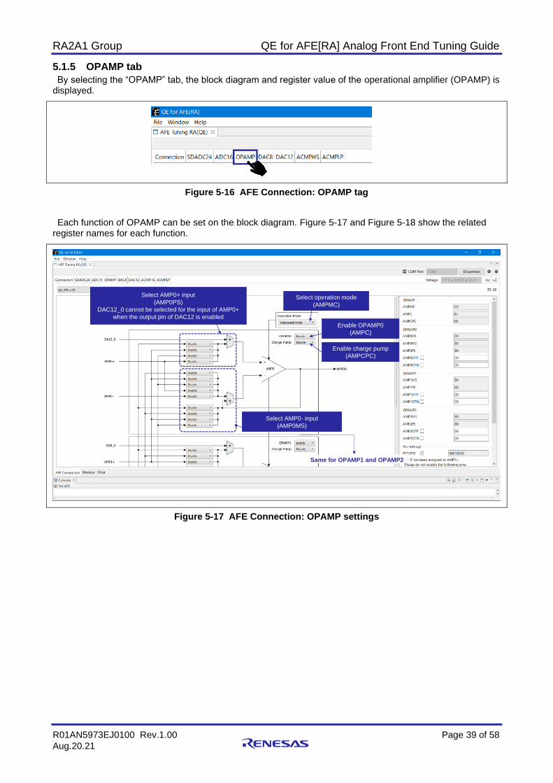
5.1.5 OPAMP tab
By selecting the “OPAMP” tab, the block diagram and register value of the operational amplifier (OPAMP) is displayed.
Figure 5-16 AFE Connection: OPAMP tag
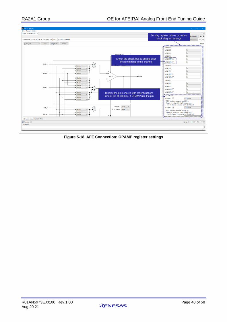
Each function of OPAMP can be set on the block diagram. Figure 5-17 and Figure 5-18 show the related register names for each function.
Figure 5-17 AFE Connection: OPAMP settings
Select AMP0+ input
(AMP0PS)
DAC12_0 cannot be selected for the input of AMP0+
when the output pin of DAC12 is enabled
Select AMP0- input
(AMP0MS)
Select operation mode
(AMPMC)
Enable OPAMP0
(AMPC)
Enable charge pump
(AMPCPC)
Same for OPAMP1 and OPAMP2
RA2A1 Group QE for AFE[RA] Analog Front End Tuning Guide
R01AN5973EJ0100 Rev.1.00 Page 40 of 58
Aug.20.21
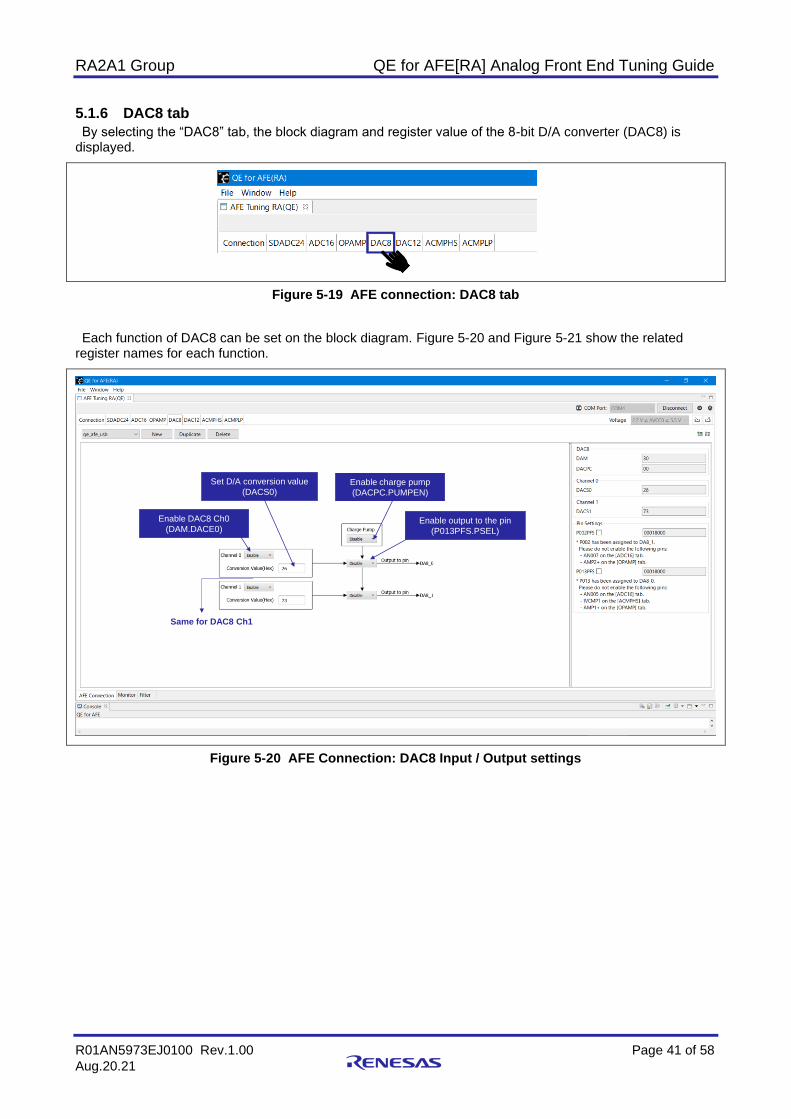
Figure 5-18 AFE Connection: OPAMP register settings
Display the pins shared with other functions
Check the check-box, if OPAMP use the pin
Check the check-box to enable user
offset trimming to the channel
Display register values based on
block diagram settings
RA2A1 Group QE for AFE[RA] Analog Front End Tuning Guide
R01AN5973EJ0100 Rev.1.00 Page 41 of 58
Aug.20.21
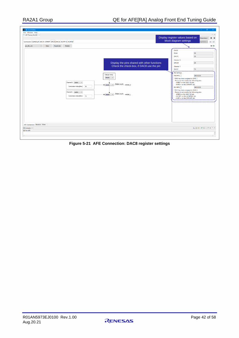
5.1.6 DAC8 tab
By selecting the “DAC8” tab, the block diagram and register value of the 8-bit D/A converter (DAC8) is displayed.
Figure 5-19 AFE connection: DAC8 tab
Each function of DAC8 can be set on the block diagram. Figure 5-20 and Figure 5-21 show the related register names for each function.
Figure 5-20 AFE Connection: DAC8 Input / Output settings
Enable DAC8 Ch0
(DAM.DACE0)
Set D/A conversion value
(DACS0)Enable charge pump
(DACPC.PUMPEN)
Enable output to the pin
(P013PFS.PSEL)
Same for DAC8 Ch1
RA2A1 Group QE for AFE[RA] Analog Front End Tuning Guide
R01AN5973EJ0100 Rev.1.00 Page 42 of 58
Aug.20.21
Figure 5-21 AFE Connection: DAC8 register settings
Display the pins shared with other functions
Check the check-box, if DAC8 use the pin
Display register values based on
block diagram settings
RA2A1 Group QE for AFE[RA] Analog Front End Tuning Guide
R01AN5973EJ0100 Rev.1.00 Page 43 of 58
Aug.20.21
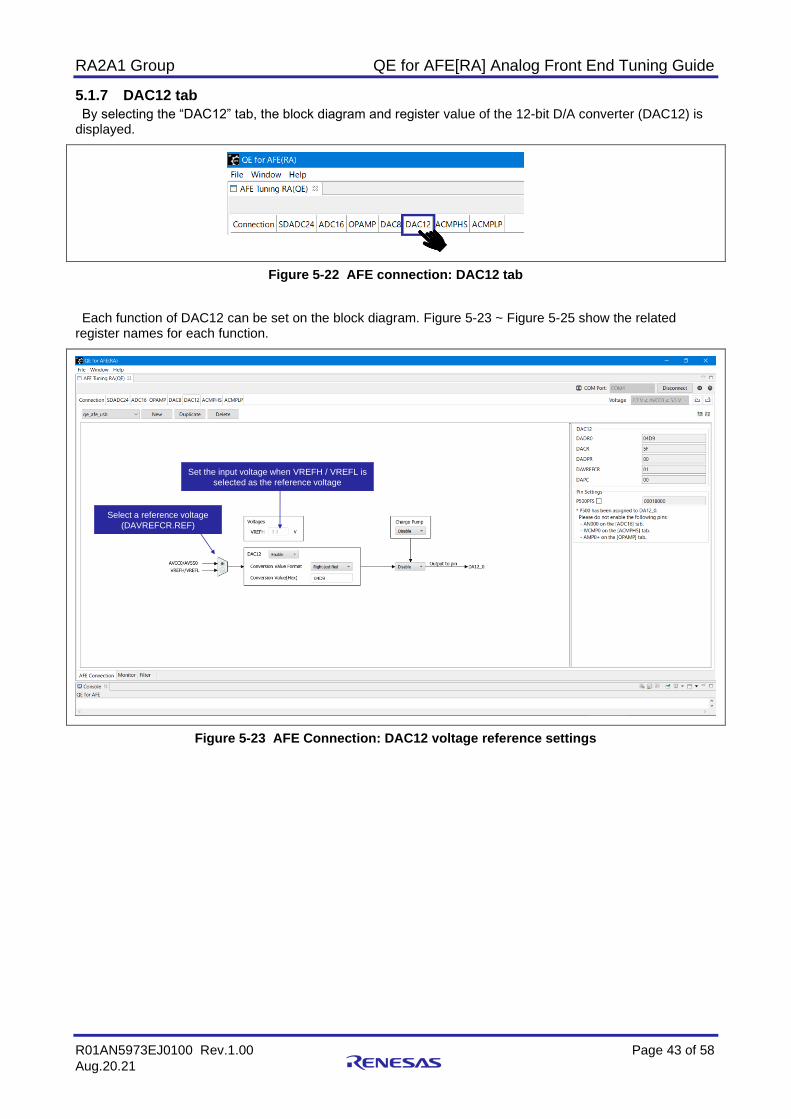
5.1.7 DAC12 tab
By selecting the “DAC12” tab, the block diagram and register value of the 12-bit D/A converter (DAC12) is displayed.
Figure 5-22 AFE connection: DAC12 tab
Each function of DAC12 can be set on the block diagram. Figure 5-23 ~ Figure 5-25 show the related register names for each function.
Figure 5-23 AFE Connection: DAC12 voltage reference settings
Set the input voltage when VREFH / VREFL is
selected as the reference voltage
Select a reference voltage
(DAVREFCR.REF)
RA2A1 Group QE for AFE[RA] Analog Front End Tuning Guide
R01AN5973EJ0100 Rev.1.00 Page 44 of 58
Aug.20.21
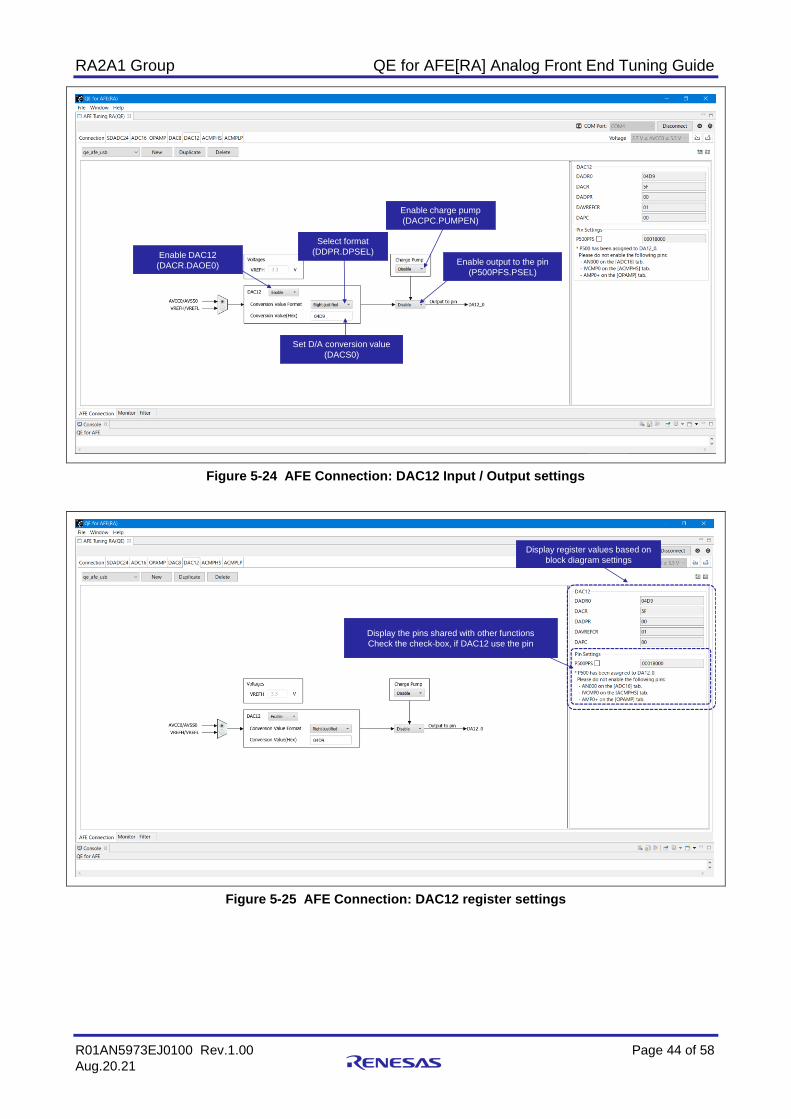
Figure 5-24 AFE Connection: DAC12 Input / Output settings
Figure 5-25 AFE Connection: DAC12 register settings
Enable DAC12
(DACR.DAOE0)
Set D/A conversion value
(DACS0)
Enable charge pump
(DACPC.PUMPEN)
Enable output to the pin
(P500PFS.PSEL)
Select format
(DDPR.DPSEL)
Display the pins shared with other functions
Check the check-box, if DAC12 use the pin
Display register values based on
block diagram settings
RA2A1 Group QE for AFE[RA] Analog Front End Tuning Guide
R01AN5973EJ0100 Rev.1.00 Page 45 of 58
Aug.20.21
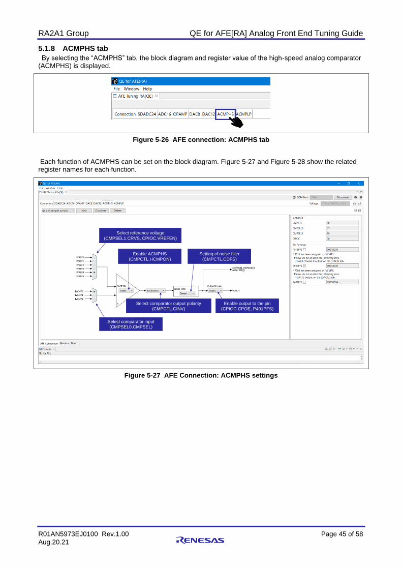
5.1.8 ACMPHS tab
By selecting the “ACMPHS” tab, the block diagram and register value of the high-speed analog comparator (ACMPHS) is displayed.
Figure 5-26 AFE connection: ACMPHS tab
Each function of ACMPHS can be set on the block diagram. Figure 5-27 and Figure 5-28 show the related register names for each function.
Figure 5-27 AFE Connection: ACMPHS settings
Select reference voltage
(CMPSEL1.CRVS, CPIOC.VREFEN)
Select comparator input
(CMPSEL0.CMPSEL)
Enable ACMPHS
(CMPCTL.HCMPON)
Select comparator output polarity
(CMPCTL.CINV)
Enable output to the pin
(CPIOC.CPOE, P401PFS)
Setting of noise filter
(CMPCTL.CDFS)
RA2A1 Group QE for AFE[RA] Analog Front End Tuning Guide
R01AN5973EJ0100 Rev.1.00 Page 46 of 58
Aug.20.21
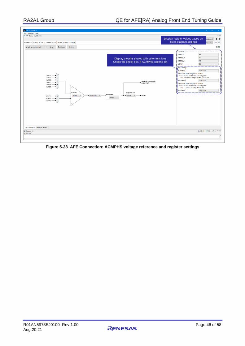
Figure 5-28 AFE Connection: ACMPHS voltage reference and register settings
Display the pins shared with other functions
Check the check-box, if ACMPHS use the pin
Display register values based on
block diagram settings
RA2A1 Group QE for AFE[RA] Analog Front End Tuning Guide
R01AN5973EJ0100 Rev.1.00 Page 47 of 58
Aug.20.21
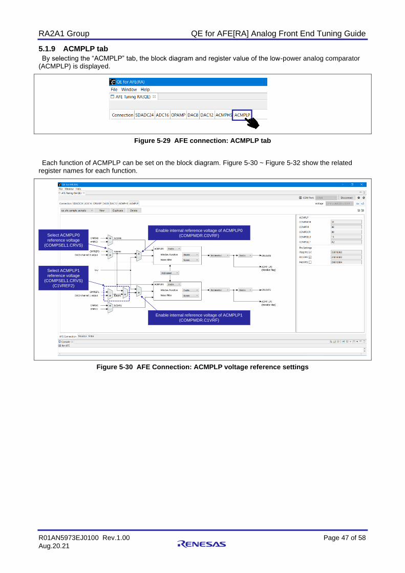
5.1.9 ACMPLP tab
By selecting the “ACMPLP” tab, the block diagram and register value of the low-power analog comparator (ACMPLP) is displayed.
Figure 5-29 AFE connection: ACMPLP tab
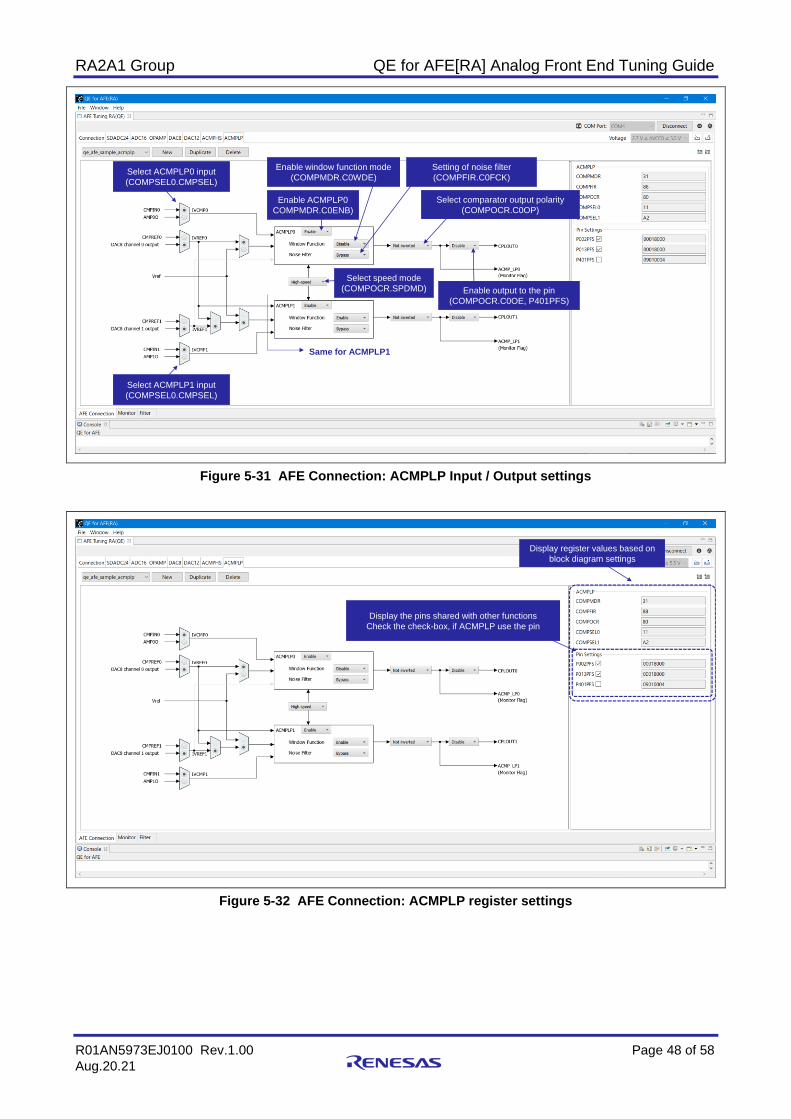
Each function of ACMPLP can be set on the block diagram. Figure 5-30 ~ Figure 5-32 show the related register names for each function.
Figure 5-30 AFE Connection: ACMPLP voltage reference settings
Select ACMPLP0
reference voltage
(COMPSEL1.CRVS)
Select ACMPLP1
reference voltage
(COMPSEL1.CRVS)
(C1VREF2)
Enable internal reference voltage of ACMPLP0
(COMPMDR.C0VRF)
Enable internal reference voltage of ACMPLP1
(COMPMDR.C1VRF)
RA2A1 Group QE for AFE[RA] Analog Front End Tuning Guide
R01AN5973EJ0100 Rev.1.00 Page 48 of 58
Aug.20.21
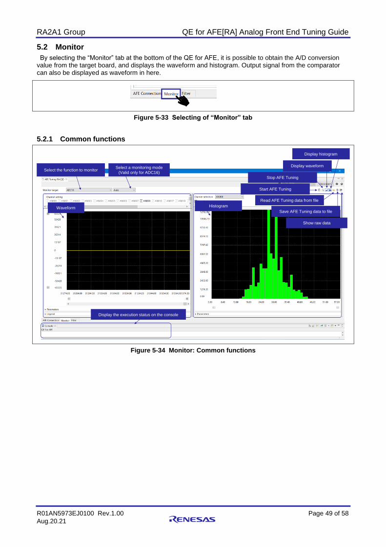
Figure 5-31 AFE Connection: ACMPLP Input / Output settings
Figure 5-32 AFE Connection: ACMPLP register settings
Select ACMPLP1 input
(COMPSEL0.CMPSEL)
Select ACMPLP0 input
(COMPSEL0.CMPSEL)
Enable ACMPLP0
COMPMDR.C0ENB)
Enable window function mode
(COMPMDR.C0WDE)
Setting of noise filter
(COMPFIR.C0FCK)
Select comparator output polarity
(COMPOCR.C0OP)
Enable output to the pin
(COMPOCR.C0OE, P401PFS)
Select speed mode
(COMPOCR.SPDMD)
Same for ACMPLP1
Display the pins shared with other functions
Check the check-box, if ACMPLP use the pin
Display register values based on
block diagram settings
RA2A1 Group QE for AFE[RA] Analog Front End Tuning Guide
R01AN5973EJ0100 Rev.1.00 Page 49 of 58
Aug.20.21
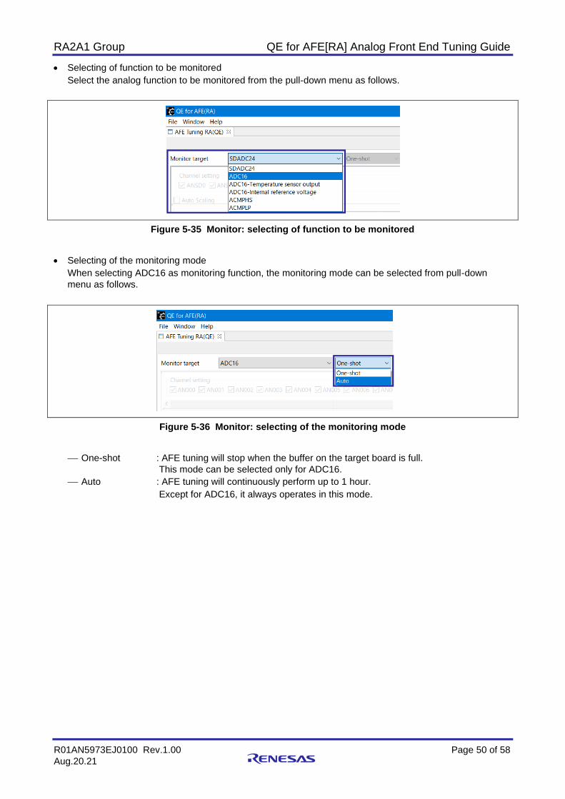
5.2 Monitor
By selecting the “Monitor” tab at the bottom of the QE for AFE, it is possible to obtain the A/D conversion value from the target board, and displays the waveform and histogram. Output signal from the comparator can also be displayed as waveform in here.
Figure 5-33 Selecting of “Monitor” tab
5.2.1 Common functions
Figure 5-34 Monitor: Common functions
Select the function to monitorSelect a monitoring mode
(Valid only for ADC16)
Display the execution status on the console
Start AFE Tuning
Stop AFE Tuning
Display waveform
Display histogram
Read AFE Tuning data from file
Save AFE Tuning data to file
Show raw data
Waveform Histogram
RA2A1 Group QE for AFE[RA] Analog Front End Tuning Guide
R01AN5973EJ0100 Rev.1.00 Page 50 of 58
Aug.20.21
• Selecting of function to be monitored
Select the analog function to be monitored from the pull-down menu as follows.
Figure 5-35 Monitor: selecting of function to be monitored
• Selecting of the monitoring mode
When selecting ADC16 as monitoring function, the monitoring mode can be selected from pull-down
menu as follows.
Figure 5-36 Monitor: selecting of the monitoring mode
⎯ One-shot : AFE tuning will stop when the buffer on the target board is full.
This mode can be selected only for ADC16.
⎯ Auto : AFE tuning will continuously perform up to 1 hour.
Except for ADC16, it always operates in this mode.
RA2A1 Group QE for AFE[RA] Analog Front End Tuning Guide
R01AN5973EJ0100 Rev.1.00 Page 51 of 58
Aug.20.21
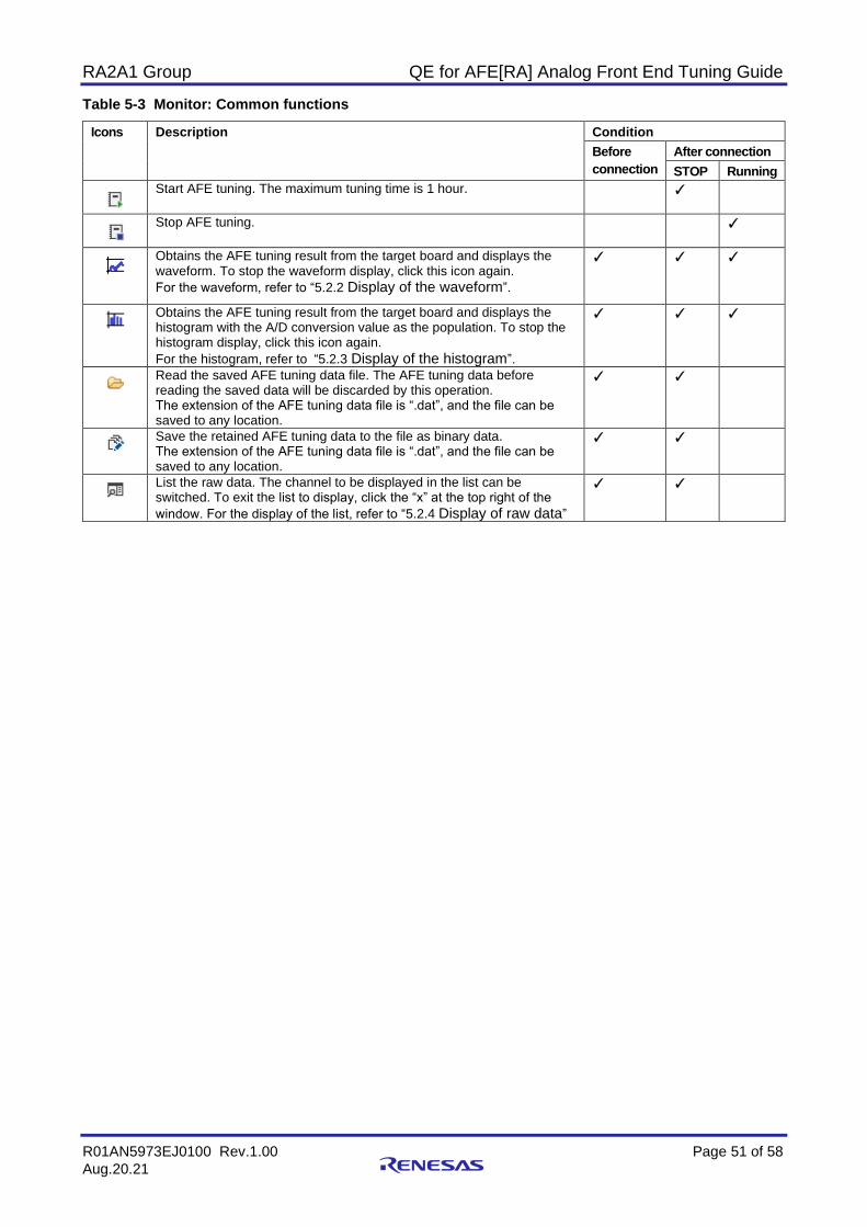
Table 5-3 Monitor: Common functions
Icons Description Condition
Before
connection
After connection
STOP Running
Start AFE tuning. The maximum tuning time is 1 hour. ✓
Stop AFE tuning. ✓
Obtains the AFE tuning result from the target board and displays the waveform. To stop the waveform display, click this icon again.
For the waveform, refer to “5.2.2 Display of the waveform”.
✓ ✓ ✓
Obtains the AFE tuning result from the target board and displays the histogram with the A/D conversion value as the population. To stop the histogram display, click this icon again.
For the histogram, refer to “5.2.3 Display of the histogram”.
✓ ✓ ✓
Read the saved AFE tuning data file. The AFE tuning data before reading the saved data will be discarded by this operation. The extension of the AFE tuning data file is “.dat”, and the file can be saved to any location.
✓ ✓
Save the retained AFE tuning data to the file as binary data. The extension of the AFE tuning data file is “.dat”, and the file can be saved to any location.
✓ ✓
List the raw data. The channel to be displayed in the list can be switched. To exit the list to display, click the “x” at the top right of the
window. For the display of the list, refer to “5.2.4 Display of raw data”
✓ ✓
RA2A1 Group QE for AFE[RA] Analog Front End Tuning Guide
R01AN5973EJ0100 Rev.1.00 Page 52 of 58
Aug.20.21
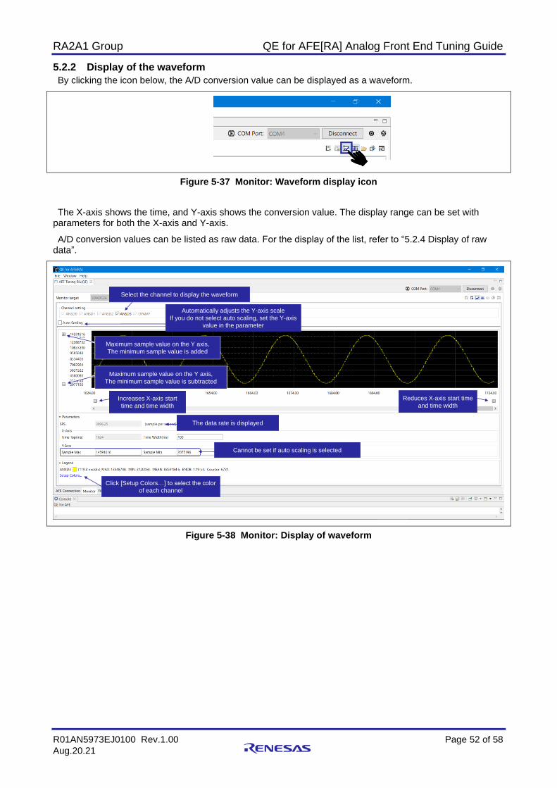
5.2.2 Display of the waveform
By clicking the icon below, the A/D conversion value can be displayed as a waveform.
Figure 5-37 Monitor: Waveform display icon
The X-axis shows the time, and Y-axis shows the conversion value. The display range can be set with parameters for both the X-axis and Y-axis.
A/D conversion values can be listed as raw data. For the display of the list, refer to “5.2.4 Display of raw data”.
Figure 5-38 Monitor: Display of waveform
Select the channel to display the waveform
Automatically adjusts the Y-axis scale
If you do not select auto scaling, set the Y-axis
value in the parameter
スケーリングを選択します(Linear, Log)
Maximum sample value on the Y axis,
The minimum sample value is added
スケーリングを選択します(Linear, Log)
Maximum sample value on the Y axis,
The minimum sample value is subtracted
The data rate is displayed
Increases X-axis start
time and time width
Cannot be set if auto scaling is selected
Reduces X-axis start time
and time width
Click [Setup Colors…] to select the color
of each channel
RA2A1 Group QE for AFE[RA] Analog Front End Tuning Guide
R01AN5973EJ0100 Rev.1.00 Page 53 of 58
Aug.20.21
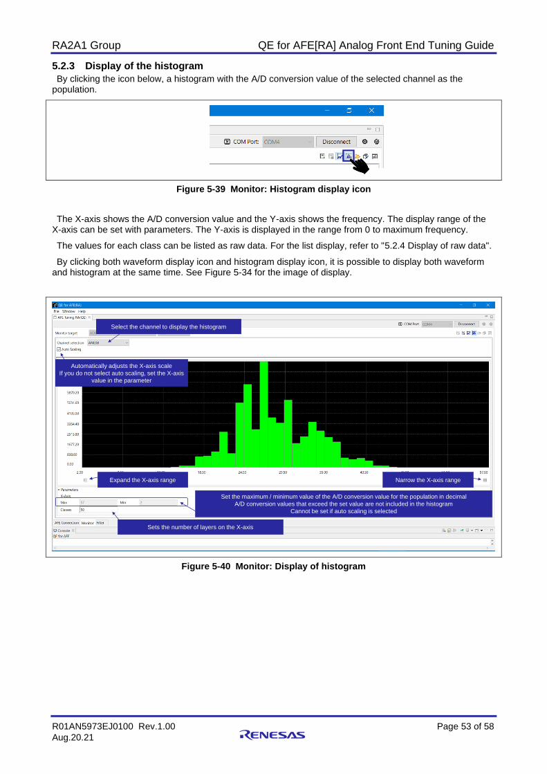
5.2.3 Display of the histogram
By clicking the icon below, a histogram with the A/D conversion value of the selected channel as the population.
Figure 5-39 Monitor: Histogram display icon
The X-axis shows the A/D conversion value and the Y-axis shows the frequency. The display range of the X-axis can be set with parameters. The Y-axis is displayed in the range from 0 to maximum frequency.
The values for each class can be listed as raw data. For the list display, refer to "5.2.4 Display of raw data".
By clicking both waveform display icon and histogram display icon, it is possible to display both waveform and histogram at the same time. See Figure 5-34 for the image of display.
Figure 5-40 Monitor: Display of histogram
Select the channel to display the histogram
Automatically adjusts the X-axis scale
If you do not select auto scaling, set the X-axis
value in the parameter
Narrow the X-axis rangeExpand the X-axis range
Sets the number of layers on the X-axis
Set the maximum / minimum value of the A/D conversion value for the population in decimal
A/D conversion values that exceed the set value are not included in the histogram
Cannot be set if auto scaling is selected
RA2A1 Group QE for AFE[RA] Analog Front End Tuning Guide
R01AN5973EJ0100 Rev.1.00 Page 54 of 58
Aug.20.21
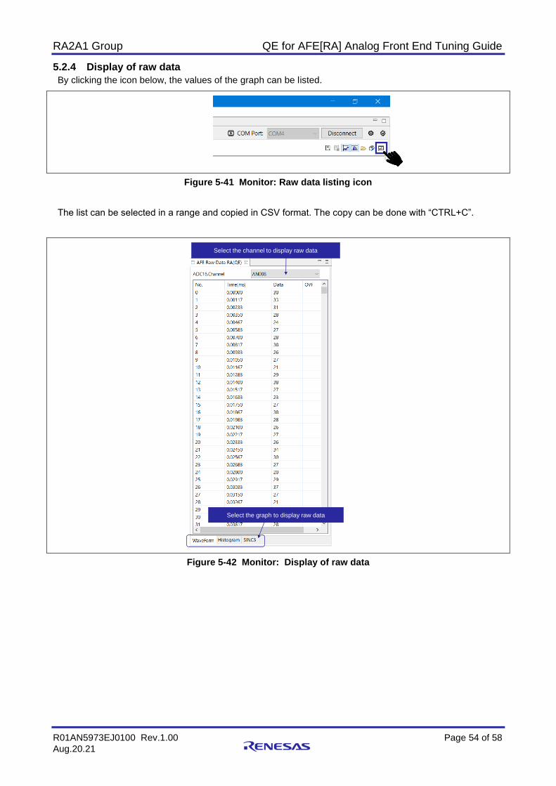
5.2.4 Display of raw data
By clicking the icon below, the values of the graph can be listed.
Figure 5-41 Monitor: Raw data listing icon
The list can be selected in a range and copied in CSV format. The copy can be done with “CTRL+C”.
Figure 5-42 Monitor: Display of raw data
Select the channel to display raw data
Select the graph to display raw data
RA2A1 Group QE for AFE[RA] Analog Front End Tuning Guide
R01AN5973EJ0100 Rev.1.00 Page 55 of 58
Aug.20.21
5.3 Filter
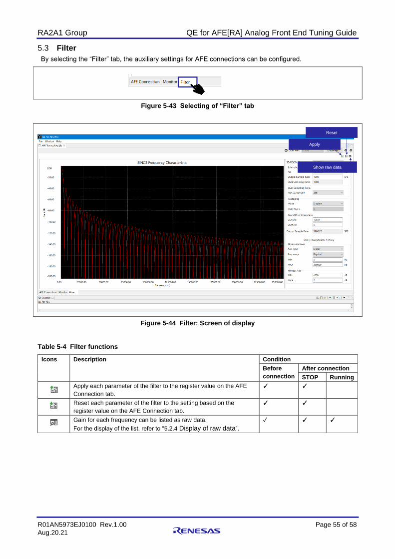
By selecting the “Filter” tab, the auxiliary settings for AFE connections can be configured.
Figure 5-43 Selecting of “Filter” tab
Figure 5-44 Filter: Screen of display
Table 5-4 Filter functions
Icons Description Condition
Before
connection
After connection
STOP Running
Apply each parameter of the filter to the register value on the AFE
Connection tab.
✓ ✓
Reset each parameter of the filter to the setting based on the
register value on the AFE Connection tab.
✓ ✓
Gain for each frequency can be listed as raw data.
For the display of the list, refer to “5.2.4 Display of raw data”.
✓ ✓ ✓
Apply
Reset
Show raw data
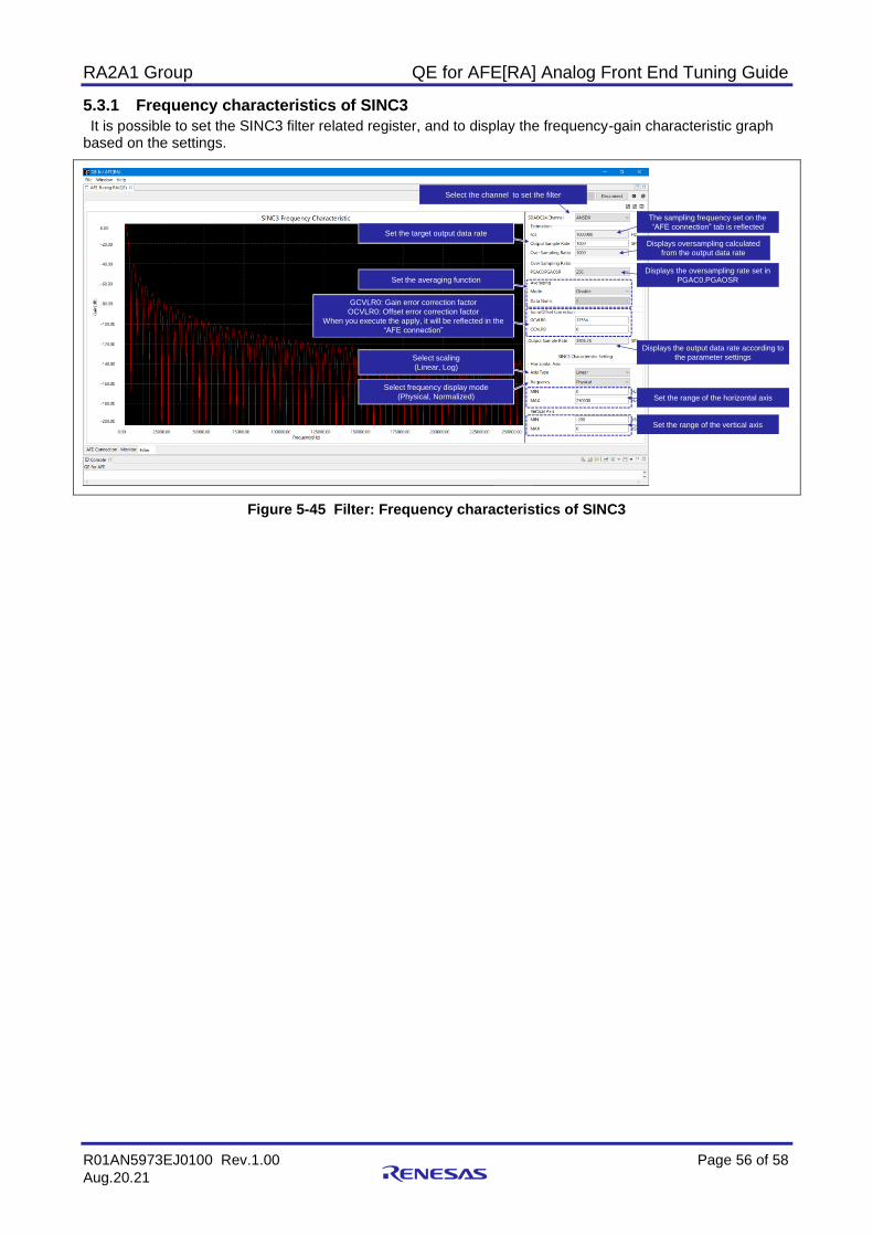
RA2A1 Group QE for AFE[RA] Analog Front End Tuning Guide
R01AN5973EJ0100 Rev.1.00 Page 56 of 58
Aug.20.21
5.3.1 Frequency characteristics of SINC3
It is possible to set the SINC3 filter related register, and to display the frequency-gain characteristic graph based on the settings.
Figure 5-45 Filter: Frequency characteristics of SINC3
Select the channel to set the filter
スケーリングを選択します(Linear, Log)Select scaling
(Linear, Log)
スケーリングを選択します(Linear, Log)
Select frequency display mode
(Physical, Normalized)
スケーリングを選択します(Linear, Log)
GCVLR0: Gain error correction factor
OCVLR0: Offset error correction factor
When you execute the apply, it will be reflected in the
“AFE connection”
スケーリングを選択します(Linear, Log)
Set the averaging function
スケーリングを選択します(Linear, Log)
Set the target output data rate
The sampling frequency set on the
“AFE connection” tab is reflected
Displays oversampling calculated
from the output data rate
Displays the oversampling rate set in
PGAC0.PGAOSR
Displays the output data rate according to
the parameter settings
Set the range of the horizontal axis
Set the range of the vertical axis
RA2A1 Group QE for AFE[RA] Analog Front End Tuning Guide
R01AN5973EJ0100 Rev.1.00 Page 57 of 58
Aug.20.21
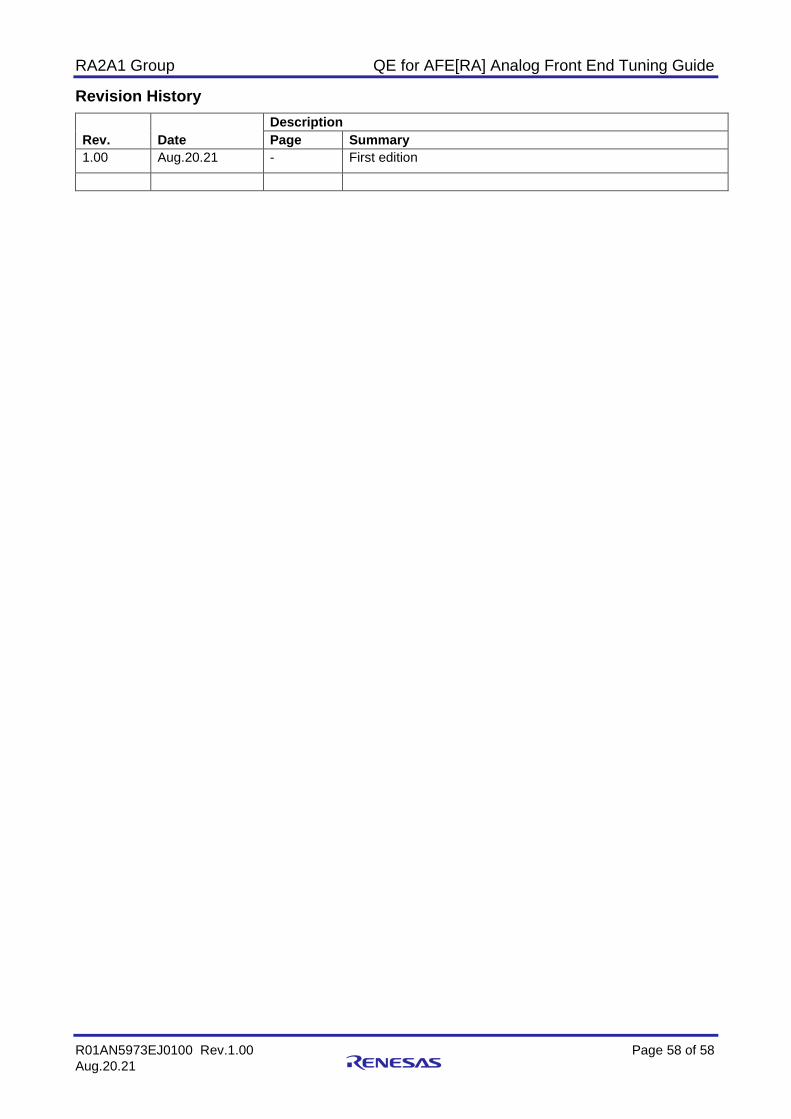
5.4 Calibration
After connecting the QE for AFE to the target board, by clicking the icon below, the calibration of analog characteristic can be done.
Figure 5-46 Calibration icon
The calibration can be done for each channel. After selecting the function and channel to perform calibration, click “Next” to display the calibration result as shown below.
Figure 5-47 Display of calibration result
Click “Finish” to reflect the register values in SINC3 and AFE Connections.
To reflect the calibration result to related registers, check the checkbox of the register to be calibrated in “AFE connection”, and make sure to write to RA2A1 on the target board.
Figure 5-48 Calibration: Reflection to the AFE connection register value
キャリブレーション結果が表示されます
The calibration result is
displayed.
The calibration result is reflectedCheck the check-box to enable
RA2A1 Group QE for AFE[RA] Analog Front End Tuning Guide
R01AN5973EJ0100 Rev.1.00 Page 58 of 58
Aug.20.21
Revision History
Rev. Date
Description
Page Summary
1.00 Aug.20.21 - First edition

General Precautions in the Handling of Microprocessing Unit and Microcontroller Unit Products
The following usage notes are applicable to all Microprocessing unit and Microcontroller unit products from Renesas. For detailed usage notes on the products covered by this document, refer to the relevant sections of the document as well as any technical updates that have been issued for the products.
1. Precaution against Electrostatic Discharge (ESD)
A strong electrical field, when exposed to a CMOS device, can cause destruction of the gate oxide and ultimately degrade the device operation. Steps
must be taken to stop the generation of static electricity as much as possible, and quickly dissipate it when it occurs. Environmental control must be
adequate. When it is dry, a humidifier should be used. This is recommended to avoid using insulators that can easily build up static electricity.
Semiconductor devices must be stored and transported in an anti-static container, static shielding bag or conductive material. All test and
measurement tools including work benches and floors must be grounded. The operator must also be grounded using a wrist strap. Semiconductor
devices must not be touched with bare hands. Similar precautions must be taken for printed circuit boards with mounted semiconductor devices.
2. Processing at power-on
The state of the product is undefined at the time when power is supplied. The states of internal circuits in the LSI are indeterminate and the states of
register settings and pins are undefined at the time when power is supplied. In a finished product where the reset signal is applied to the external reset
pin, the states of pins are not guaranteed from the time when power is supplied until the reset process is completed. In a similar way, the states of pins
in a product that is reset by an on-chip power-on reset function are not guaranteed from the time when power is supplied until the power reaches the
level at which resetting is specified.
3. Input of signal during power-off state
Do not input signals or an I/O pull-up power supply while the device is powered off. The current injection that results from input of such a signal or I/O
pull-up power supply may cause malfunction and the abnormal current that passes in the device at this time may cause degradation of internal
elements. Follow the guideline for input signal during power-off state as described in your product documentation.
4. Handling of unused pins
Handle unused pins in accordance with the directions given under handling of unused pins in the manual. The input pins of CMOS products are
generally in the high-impedance state. In operation with an unused pin in the open-circuit state, extra electromagnetic noise is induced in the vicinity of
the LSI, an associated shoot-through current flows internally, and malfunctions occur due to the false recognition of the pin state as an input signal
become possible.
5. Clock signals
After applying a reset, only release the reset line after the operating clock signal becomes stable. When switching the clock signal during program
execution, wait until the target clock signal is stabilized. When the clock signal is generated with an external resonator or from an external oscillator
during a reset, ensure that the reset line is only released after full stabilization of the clock signal. Additionally, when switching to a clock signal
produced with an external resonator or by an external oscillator while program execution is in progress, wait until the target clock signal is stable.
6. Voltage application waveform at input pin
Waveform distortion due to input noise or a reflected wave may cause malfunction. If the input of the CMOS device stays in the area between VIL
(Max.) and VIH (Min.) due to noise, for example, the device may malfunction. Take care to prevent chattering noise from entering the device when the
input level is fixed, and also in the transition period when the input level passes through the area between VIL (Max.) and VIH (Min.).
7. Prohibition of access to reserved addresses
Access to reserved addresses is prohibited. The reserved addresses are provided for possible future expansion of functions. Do not access these
addresses as the correct operation of the LSI is not guaranteed.
8. Differences between products
Before changing from one product to another, for example to a product with a different part number, confirm that the change will not lead to problems.
The characteristics of a microprocessing unit or microcontroller unit products in the same group but having a different part number might differ in terms
of internal memory capacity, layout pattern, and other factors, which can affect the ranges of electrical characteristics, such as characteristic values,
operating margins, immunity to noise, and amount of radiated noise. When changing to a product with a different part number, implement a system-
evaluation test for the given product.

© 2021 Renesas Electronics Corporation. All rights reserved.
Notice
1. Descriptions of circuits, software and other related information in this document are provided only to illustrate the operation of semiconductor products
and application examples. You are fully responsible for the incorporation or any other use of the circuits, software, and information in the design of your
product or system. Renesas Electronics disclaims any and all liability for any losses and damages incurred by you or third parties arising from the use
of these circuits, software, or information.
2. Renesas Electronics hereby expressly disclaims any warranties against and liability for infringement or any other claims involving patents, copyrights,
or other intellectual property rights of third parties, by or arising from the use of Renesas Electronics products or technical information described in this
document, including but not limited to, the product data, drawings, charts, programs, algorithms, and application examples.
3. No license, express, implied or otherwise, is granted hereby under any patents, copyrights or other intellectual property rights of Renesas Electronics
or others.
4. You shall be responsible for determining what licenses are required from any third parties, and obtaining such licenses for the lawful import, export,
manufacture, sales, utilization, distribution or other disposal of any products incorporating Renesas Electronics products, if required.
5. You shall not alter, modify, copy, or reverse engineer any Renesas Electronics product, whether in whole or in part. Renesas Electronics disclaims any
and all liability for any losses or damages incurred by you or third parties arising from such alteration, modification, copying or reverse engineering.
6. Renesas Electronics products are classified according to the following two quality grades: “Standard” and “High Quality”. The intended applications for
each Renesas Electronics product depends on the product’s quality grade, as indicated below.
"Standard": Computers; office equipment; communications equipment; test and measurement equipment; audio and visual equipment; home
electronic appliances; machine tools; personal electronic equipment; industrial robots; etc.
"High Quality": Transportation equipment (automobiles, trains, ships, etc.); traffic control (traffic lights); large-scale communication equipment; key
financial terminal systems; safety control equipment; etc.
Unless expressly designated as a high reliability product or a product for harsh environments in a Renesas Electronics data sheet or other Renesas
Electronics document, Renesas Electronics products are not intended or authorized for use in products or systems that may pose a direct threat to
human life or bodily injury (artificial life support devices or systems; surgical implantations; etc.), or may cause serious property damage (space
system; undersea repeaters; nuclear power control systems; aircraft control systems; key plant systems; military equipment; etc.). Renesas Electronics
disclaims any and all liability for any damages or losses incurred by you or any third parties arising from the use of any Renesas Electronics product
that is inconsistent with any Renesas Electronics data sheet, user’s manual or other Renesas Electronics document.
7. No semiconductor product is absolutely secure. Notwithstanding any security measures or features that may be implemented in Renesas Electronics
hardware or software products, Renesas Electronics shall have absolutely no liability arising out of any vulnerability or security breach, including but
not limited to any unauthorized access to or use of a Renesas Electronics product or a system that uses a Renesas Electronics product. RENESAS
ELECTRONICS DOES NOT WARRANT OR GUARANTEE THAT RENESAS ELECTRONICS PRODUCTS, OR ANY SYSTEMS CREATED USING
RENESAS ELECTRONICS PRODUCTS WILL BE INVULNERABLE OR FREE FROM CORRUPTION, ATTACK, VIRUSES, INTERFERENCE,
HACKING, DATA LOSS OR THEFT, OR OTHER SECURITY INTRUSION (“Vulnerability Issues”). RENESAS ELECTRONICS DISCLAIMS ANY AND
ALL RESPONSIBILITY OR LIABILITY ARISING FROM OR RELATED TO ANY VULNERABILITY ISSUES. FURTHERMORE, TO THE EXTENT
PERMITTED BY APPLICABLE LAW, RENESAS ELECTRONICS DISCLAIMS ANY AND ALL WARRANTIES, EXPRESS OR IMPLIED, WITH
RESPECT TO THIS DOCUMENT AND ANY RELATED OR ACCOMPANYING SOFTWARE OR HARDWARE, INCLUDING BUT NOT LIMITED TO
THE IMPLIED WARRANTIES OF MERCHANTABILITY, OR FITNESS FOR A PARTICULAR PURPOSE.
8. When using Renesas Electronics products, refer to the latest product information (data sheets, user’s manuals, application notes, “General Notes for
Handling and Using Semiconductor Devices” in the reliability handbook, etc.), and ensure that usage conditions are within the ranges specified by
Renesas Electronics with respect to maximum ratings, operating power supply voltage range, heat dissipation characteristics, installation, etc. Renesas
Electronics disclaims any and all liability for any malfunctions, failure or accident arising out of the use of Renesas Electronics products outside of such
specified ranges.
9. Although Renesas Electronics endeavors to improve the quality and reliability of Renesas Electronics products, semiconductor products have specific
characteristics, such as the occurrence of failure at a certain rate and malfunctions under certain use conditions. Unless designated as a high reliability
product or a product for harsh environments in a Renesas Electronics data sheet or other Renesas Electronics document, Renesas Electronics
products are not subject to radiation resistance design. You are responsible for implementing safety measures to guard against the possibility of bodily
injury, injury or damage caused by fire, and/or danger to the public in the event of a failure or malfunction of Renesas Electronics products, such as
safety design for hardware and software, including but not limited to redundancy, fire control and malfunction prevention, appropriate treatment for
aging degradation or any other appropriate measures. Because the evaluation of microcomputer software alone is very difficult and impractical, you are
responsible for evaluating the safety of the final products or systems manufactured by you.
10. Please contact a Renesas Electronics sales office for details as to environmental matters such as the environmental compatibility of each Renesas
Electronics product. You are responsible for carefully and sufficiently investigating applicable laws and regulations that regulate the inclusion or use of
controlled substances, including without limitation, the EU RoHS Directive, and using Renesas Electronics products in compliance with all these
applicable laws and regulations. Renesas Electronics disclaims any and all liability for damages or losses occurring as a result of your noncompliance
with applicable laws and regulations.
11. Renesas Electronics products and technologies shall not be used for or incorporated into any products or systems whose manufacture, use, or sale is
prohibited under any applicable domestic or foreign laws or regulations. You shall comply with any applicable export control laws and regulations
promulgated and administered by the governments of any countries asserting jurisdiction over the parties or transactions.
12. It is the responsibility of the buyer or distributor of Renesas Electronics products, or any other party who distributes, disposes of, or otherwise sells or
transfers the product to a third party, to notify such third party in advance of the contents and conditions set forth in this document.
13. This document shall not be reprinted, reproduced or duplicated in any form, in whole or in part, without prior written consent of Renesas Electronics.
14. Please contact a Renesas Electronics sales office if you have any questions regarding the information contained in this document or Renesas
Electronics products.
(Note1) “Renesas Electronics” as used in this document means Renesas Electronics Corporation and also includes its directly or indirectly controlled
subsidiaries.
(Note2) “Renesas Electronics product(s)” means any product developed or manufactured by or for Renesas Electronics.
(Rev.5.0-1 October 2020)
Corporate Headquarters Contact information TOYOSU FORESIA, 3-2-24 Toyosu,
Koto-ku, Tokyo 135-0061, Japan
www.renesas.com
For further information on a product, technology, the most up-to-date
version of a document, or your nearest sales office, please visit:
www.renesas.com/contact/.
Trademarks
Renesas and the Renesas logo are trademarks of Renesas Electronics
Corporation. All trademarks and registered trademarks are the property
of their respective owners.