isolated flyback converter -...
TRANSCRIPT

O Product structure : silicon monolithic integrated circuit O This product has no designed protection against radioactive rays
1/27
TSZ02201-0J1J0AZ01220-1-2 © 2016 ROHM Co., Ltd. All rights reserved. 17.Apr.2017 Rev.003
www.rohm.com
TSZ22111・14・001
Optocoupler-less
Isolated Flyback Converter BD7F200HFN-LB BD7F200EFJ-LB
General Description This product guarantees long time supply availability in the industrial instrumentation market.
BD7F200 is an optocoupler-less Isolated Flyback Converter. An optocoupler or the tertiary winding feedback circuit which was needed to obtain a stable output voltage isolated by a transformer in the conventional application becomes unnecessary, thus, the number of parts is reduced drastically, producing a small-sized and high-reliability application isolated type power supply. Furthermore, a highly by the use of the Original Adapted-Type ON-Time Control Technology, it makes the external phase compensation parts become unnecessary, therefore a highly efficient isolated type power supply application can easily be produced.
Features Guaranteed long time supply availability for
Industrial Applications. No need for an optocoupler or a transformer tertiary
winding. The output voltage can be set by two external resistors and the transformer turns ratio.
Uses Original Adapted Type ON-Time Control Technology. High-speed load response is realized and external phase compensation parts are unnecessary.
Fixed switching frequency and low output ripple Highly efficient light load mode available (PFM
operation) Shutdown / Enable Control Built-in N-Channel MOSFET Soft start function Output load compensation function Protection functions:
VIN Under Voltage Lock-Out (VIN UVLO) Over Current Protection (OCP) Thermal Shutdown Protection (TSD)
Application Industrial equipment Isolated Power Supply
Key Specifications Supply Voltage of Operation: 8V to 40V SW Terminal Operating Voltage: 50V (Max) Over Current Limit: 2.75A (Typ) Switching Frequency: 400kHz (Typ) Reference Voltage Accuracy: ±1.5% (Typ) Quiescent Current: 0µA (Typ) Operating Current: 2mA (Typ) Junction Temperature of Operation: -40°C to +125°C
Packages W(Typ) D(Typ) H(Max)
HSON8 2.90mm x 3.00mm x 0.60mm HTSOP-J8 4.90mm x 6.00mm x 1.00mm
HSON8 HTSOP-J8
Datasheet
2/27
BD7F200HFN-LB BD7F200EFJ-LB
TSZ02201-0J1J0AZ01220-1-2
© 2016 ROHM Co., Ltd. All rights reserved. 17.Apr.2017 Rev.003
www.rohm.com
TSZ22111・15・001
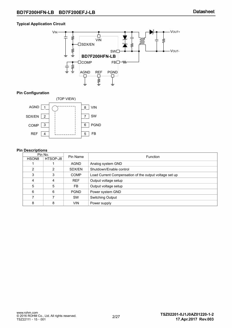
Typical Application Circuit
Pin Configuration
Pin Descriptions
Pin No. Pin Name Function
HSON8 HTSOP-J8
1 1 AGND Analog system GND
2 2 SDX/EN Shutdown/Enable control
3 3 COMP Load Current Compensation of the output voltage set up
4 4 REF Output voltage setup
5 5 FB Output voltage setup
6 6 PGND Power system GND
7 7 SW Switching Output
8 8 VIN Power supply
(TOP VIEW)
VIN
SW
FB
AGND
REF
PGND
SDX/EN
COMP
7
8
6
5
3
4
2
1
FB
SW
VIN
VOUT+
VOUT-
SDX/EN
COMP
AGND REF PGND
VIN
BD7F200HFN-LB
3/27
BD7F200HFN-LB BD7F200EFJ-LB
TSZ02201-0J1J0AZ01220-1-2
© 2016 ROHM Co., Ltd. All rights reserved. 17.Apr.2017 Rev.003
www.rohm.com
TSZ22111・15・001
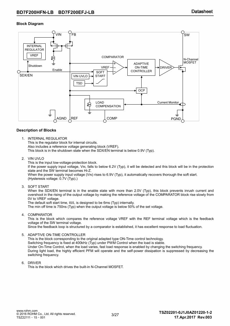
Block Diagram
FB SW
DRIVER
ADAPTIVE
ON-TIME
CONTROLLER
VREF
SOFT
START
COMPARATOR
VIN
INTERNAL
REGULATOR
SDX/EN
LOAD
COMPENSATION
VIN UVLO
PGNDCOMPREFAGND
N-ChannelMOSFET
Shutdown
OCP
TSD
Enable
VREF
Current Monitor
Description of Blocks
1. INTERNAL REGULATOR This is the regulator block for internal circuits. Also includes a reference voltage generating block (VREF). This block is in the shutdown state when the SDX/EN terminal is below 0.9V (Typ).
2. VIN UVLO
This is the input low-voltage-protection block. If the power supply input voltage, VIN, falls to below 6.2V (Typ), it will be detected and this block will be in the protection state and the SW terminal becomes Hi-Z. When the power supply input voltage (VIN) rises to 6.9V (Typ), it automatically recovers thorough the soft start. (Hysteresis voltage: 0.7V (Typ).)
3. SOFT START When the SDX/EN terminal is in the enable state with more than 2.0V (Typ), this block prevents inrush current and overshoot in the rising of the output voltage by making the reference voltage of the COMPARATOR block rise slowly from 0V to VREF voltage. The default soft start time, tSS, is designed to be 6ms (Typ) internally. The min off time is 750ns (Typ) when the output voltage is below 50% of the set voltage.
4. COMPARATOR
This is the block which compares the reference voltage VREF with the REF terminal voltage which is the feedback voltage of the SW terminal voltage. Since the feedback loop is structured by a comparator is established, it has excellent response to load fluctuation.
5. ADAPTIVE ON-TIME CONTROLLER
This is the block corresponding to the original adapted type ON-Time control technology. Switching frequency is fixed at 400kHz (Typ) under PWM Control when the load is stable. Under On-Time Control, when the load varies, fast load response is enabled by changing the switching frequency. During light load, the highly efficient PFM will operate and the self-power dissipation is suppressed by decreasing the switching frequency.
6. DRIVER
This is the block which drives the built-in N-Channel MOSFET.
4/27
BD7F200HFN-LB BD7F200EFJ-LB
TSZ02201-0J1J0AZ01220-1-2
© 2016 ROHM Co., Ltd. All rights reserved. 17.Apr.2017 Rev.003
www.rohm.com
TSZ22111・15・001
Description of Blocks - continued 7. LOAD COMPENSATION
This is the block which compensates the output voltage regulation by VF characteristic fluctuation of the secondary side output diode according to the load current. The current which flows into the built-in N-Channel MOSFET is monitored, and the current according to the compensation quantity and the time constant which are determined by the external resistor and the capacitor of the COMP terminal is drawn from the REF terminal. The output voltage rises and is rectified when feedback current which flows into the external resistor of the REF terminal decreases and the REF terminal voltage falls.
8. TSD
This is the temperature protection block. If the chip’s junction temperature, Tj, inside the IC is above 175°C (Typ), it will be detected and this block will be in the protection state and the SW terminal becomes Hi-Z. If Tj falls to below 150°C (Typ), it will return automatically through soft start.
9. OCP
This is the over-current protection block. If the peak current during the ON-Time of the built-in N-Channel MOSFET reaches 2.75A (Typ), it will be detected and the N-Channel MOSFET is turned OFF. If output voltage goes to 50% or less of the setting voltage, the peak detection current of OCP will be controlled by 1.6A (Typ).The min off time is 1.5μs (Typ) when the OCP is operated under the condition where the output voltage is 50% of the set voltage.
Absolute Maximum Ratings (Ta = 25 °C)
Parameter Symbol Rating
Unit BD7F200HFN-LB BD7F200EFJ-LB
VIN Input Power Voltage (Note 1)
VIN 45 V
SW Terminal Voltage VSW 60 V
SDX/EN Terminal Voltage VSDX/EN VIN V
FB Terminal Voltage VFB VIN-0.3V to lower value of VIN+0.3V or 45V V
REF Terminal Voltage VREF 7 V
COMP Terminal Voltage VCOMP 7 V
Power Dissipation Pd 1.75 (Note 2)
3.75 (Note 3)
W
Storage Temperature Range Tstg -55 to +150 °C
Maximum Junction Temperature Tjmax 150 °C
(Note 1) Not to exceed Power Dissipation (Pd). (Note 2) Reduced by 14.0mW/°C for temperatures above 25°C (when mounted on a one-layer glass-epoxy board with 70mm × 70mm × 1.6mm dimension,
65% copper foil density) (Note 3) Reduced by 30.0mW/°C for temperatures above 25°C (when mounted on four-layer glass-epoxy board with 70mm × 70mm × 1.6mm dimension.) Caution: Operating the IC over the absolute maximum ratings may damage the IC. The damage can either be a short circuit between pins or an open circuit
between pins and the internal circuitry. Therefore, it is important to consider circuit protection measures, such as adding a fuse, in case the IC is operated over the absolute maximum ratings.
Recommended Operating Conditions
Parameter Symbol Limit
Unit Min Typ Max
VIN Input Power Voltage VIN 8 24 40 V
SW Terminal Voltage VSW - - 50 V
Junction Temperature (Note4)
Tj -40 - +125 °C
(Note 4) Life time is derated at junction temperature greater than 125°C.
5/27
BD7F200HFN-LB BD7F200EFJ-LB
TSZ02201-0J1J0AZ01220-1-2
© 2016 ROHM Co., Ltd. All rights reserved. 17.Apr.2017 Rev.003
www.rohm.com
TSZ22111・15・001
Electrical Characteristics (Unless otherwise specified Ta = 25°C, VIN = 24V, and VSDX/EN = 2.5V.)
Parameter Symbol Limit
Unit Conditions Min Typ Max
Power Supply
Quiescent Current IST - 0 10 µA VSDX/EN = 0V
Operating Current ICC - 2 4 mA VSDX/EN = 2.5V VREF = 2V (at PFM operation)
UVLO Detection Voltage VUVLO 5.7 6.2 6.7 V VIN falling
UVLO Hysteresis Voltage VUVLO_HYS 0.6 0.7 0.8 V
SDX/EN Control
Shutdown Voltage VSDX 0.3 0.9 1.5 V
Enable Voltage VEN 1.9 2.0 2.1 V VSDX/EN rising
Enable Hysteresis Voltage VEN_HYS 0.15 0.2 0.25 V
SDX/EN Input Current ISDX/EN - 0 1 µA VSDX/EN=2V
Reference Voltage
Reference Voltage VREF 0.768 0.78 0.792 V
Switch Characteristics
ON-Resistance RON - 0.5 - Ω Between SW - PGND terminals
Over Current Limit ILIMIT 2.2 2.75 3.3 A
Switching Frequency fSW - 400 - kHz At PWM operation (Duty=40%)
Minimum ON Time tON_MIN - 350 - ns
Minimum OFF Time tOFF_MIN - 300 - ns
Maximum OFF Time tOFF_MAX - 20 - µs
Soft Start Time tSS - 6 - ms 0V to (VREF×90%)
6/27
BD7F200HFN-LB BD7F200EFJ-LB
TSZ02201-0J1J0AZ01220-1-2
© 2016 ROHM Co., Ltd. All rights reserved. 17.Apr.2017 Rev.003
www.rohm.com
TSZ22111・15・001
Typical Performance Curves
0
2
4
6
8
10
12
14
16
18
0 5 10 15 20 25 30 35 40 45 50
Ma
xim
um
Ou
tpu
t P
ow
er [W
]
VIN Voltage [V]
Restriction by the current limit 2.2A (Min)
Restriction by the SW terminal voltage 50V (Max)
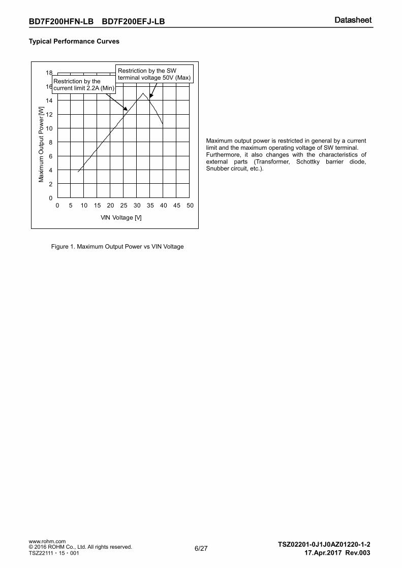
Maximum output power is restricted in general by a current limit and the maximum operating voltage of SW terminal. Furthermore, it also changes with the characteristics of external parts (Transformer, Schottky barrier diode, Snubber circuit, etc.).
Figure 1. Maximum Output Power vs VIN Voltage
7/27
BD7F200HFN-LB BD7F200EFJ-LB
TSZ02201-0J1J0AZ01220-1-2
© 2016 ROHM Co., Ltd. All rights reserved. 17.Apr.2017 Rev.003
www.rohm.com
TSZ22111・15・001
Typical Performance Curves
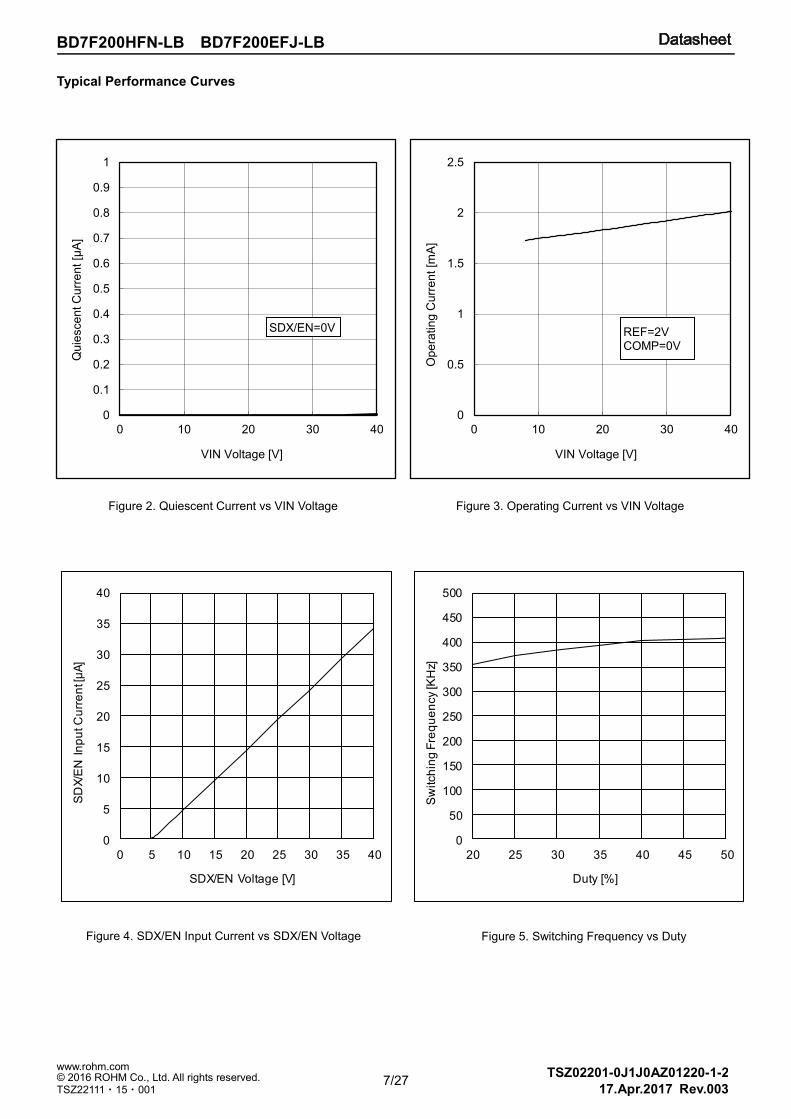
Figure 3. Operating Current vs VIN Voltage
Figure 2. Quiescent Current vs VIN Voltage
0
0.5
1
1.5
2
2.5
0 10 20 30 40O
pe
ratin
g C
urr
en
t [m
A]
VIN Voltage [V]
REF=2V COMP=0V
0
0.1
0.2
0.3
0.4
0.5
0.6
0.7
0.8
0.9
1
0 10 20 30 40
Qu
iesce
nt C
urr
en
t [μ
A]
VIN Voltage [V]
SDX/EN=0V
0
5
10
15
20
25
30
35
40
0 5 10 15 20 25 30 35 40
SD
X/E
N I
np
ut C
urr
en
t [μ
A]
SDX/EN Voltage [V]
Figure 4. SDX/EN Input Current vs SDX/EN Voltage
0
50
100
150
200
250
300
350
400
450
500
20 25 30 35 40 45 50
Sw
itch
ing
Fre
qu
en
cy
[KH
z]
Duty [%]
Figure 5. Switching Frequency vs Duty
8/27
BD7F200HFN-LB BD7F200EFJ-LB
TSZ02201-0J1J0AZ01220-1-2
© 2016 ROHM Co., Ltd. All rights reserved. 17.Apr.2017 Rev.003
www.rohm.com
TSZ22111・15・001
Typical Performance Curves
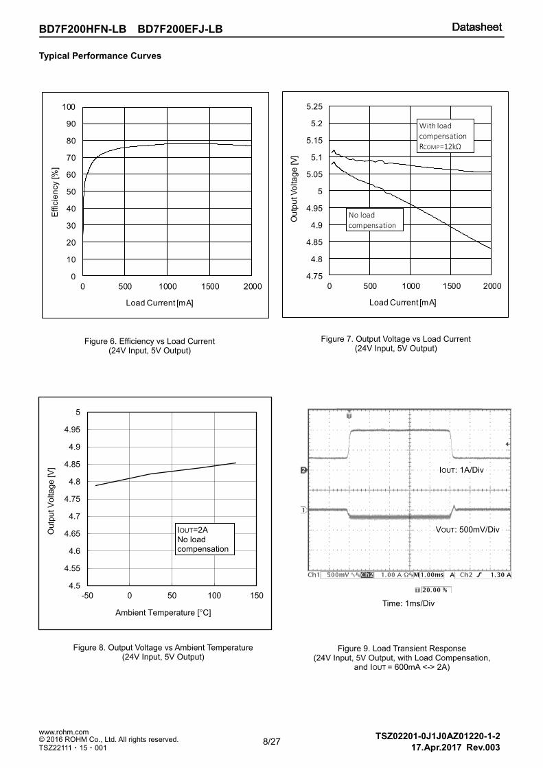
Figure 9. Load Transient Response (24V Input, 5V Output, with Load Compensation,
and IOUT = 600mA <-> 2A)
Figure 6. Efficiency vs Load Current (24V Input, 5V Output)
0
10
20
30
40
50
60
70
80
90
100
0 500 1000 1500 2000
Effic
ien
cy
[%]
Load Current [mA]
4.5
4.55
4.6
4.65
4.7
4.75
4.8
4.85
4.9
4.95
5
-50 0 50 100 150
Ou
tpu
t V
olta
ge
[V
]
Ambient Temperature [°C]
IOUT=2A No load compensation
Figure 7. Output Voltage vs Load Current (24V Input, 5V Output)
4.75
4.8
4.85
4.9
4.95
5
5.05
5.1
5.15
5.2
5.25
0 500 1000 1500 2000O
utp
ut V
olta
ge
[V
]
Load Current [mA]
With load
compensation
RCOMP=12kΩ
No load
compensation
Figure 8. Output Voltage vs Ambient Temperature (24V Input, 5V Output)
IOUT: 1A/Div
VOUT: 500mV/Div
Time: 1ms/Div
9/27
BD7F200HFN-LB BD7F200EFJ-LB
TSZ02201-0J1J0AZ01220-1-2
© 2016 ROHM Co., Ltd. All rights reserved. 17.Apr.2017 Rev.003
www.rohm.com
TSZ22111・15・001
Typical Performance Curves
VIN: 20V/Div
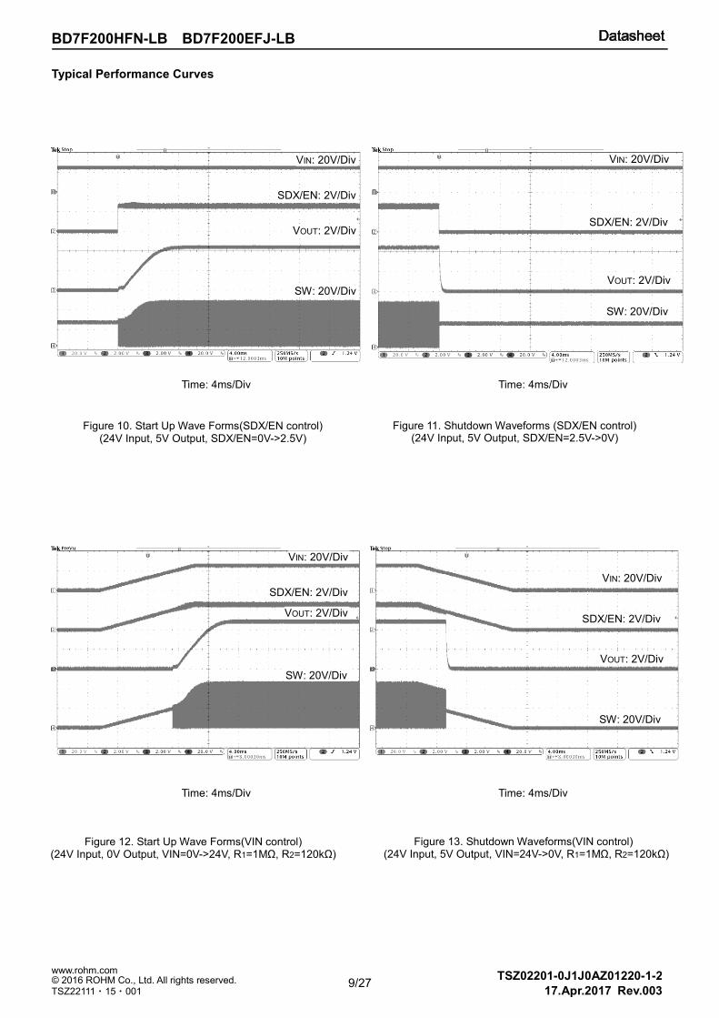
Figure 10. Start Up Wave Forms(SDX/EN control) (24V Input, 5V Output, SDX/EN=0V->2.5V)
VIN: 20V/Div
SDX/EN: 2V/Div
VOUT: 2V/Div
SW: 20V/Div
Figure 11. Shutdown Waveforms (SDX/EN control) (24V Input, 5V Output, SDX/EN=2.5V->0V)
Time: 4ms/Div
VIN: 20V/Div
SDX/EN: 2V/Div
VOUT: 2V/Div
SW: 20V/Div
Time: 4ms/Div
Figure 13. Shutdown Waveforms(VIN control) (24V Input, 5V Output, VIN=24V->0V, R1=1MΩ, R2=120kΩ)
Figure 12. Start Up Wave Forms(VIN control) (24V Input, 0V Output, VIN=0V->24V, R1=1MΩ, R2=120kΩ)
SDX/EN: 2V/Div
VOUT: 2V/Div
SW: 20V/Div
VIN: 20V/Div
SDX/EN: 2V/Div
VOUT: 2V/Div
SW: 20V/Div
Time: 4ms/Div Time: 4ms/Div
10/27
BD7F200HFN-LB BD7F200EFJ-LB
TSZ02201-0J1J0AZ01220-1-2
© 2016 ROHM Co., Ltd. All rights reserved. 17.Apr.2017 Rev.003
www.rohm.com
TSZ22111・15・001
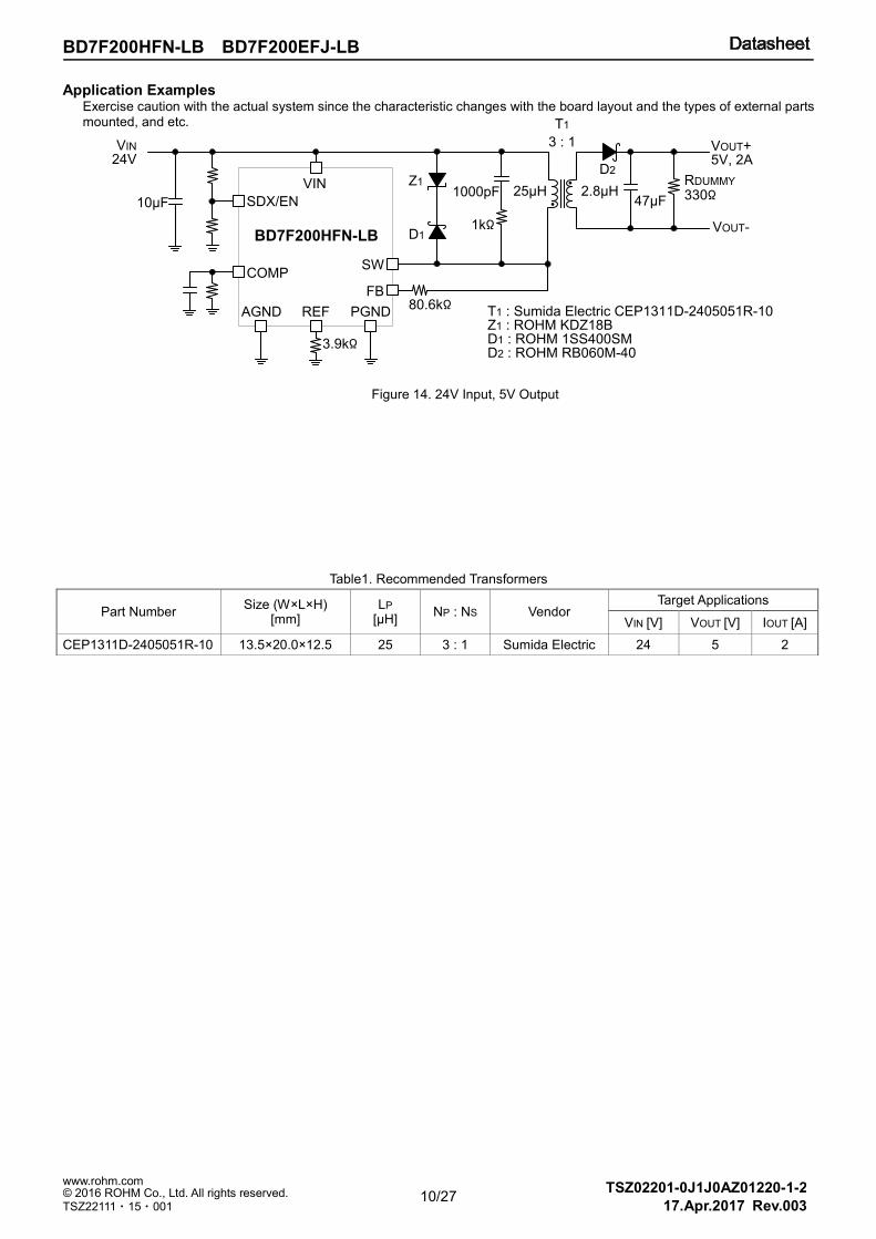
Application Examples Exercise caution with the actual system since the characteristic changes with the board layout and the types of external parts mounted, and etc.
Table1. Recommended Transformers
Part Number Size (W×L×H)
[mm] LP
[μH] NP : NS Vendor
Target Applications
VIN [V] VOUT [V] IOUT [A]
CEP1311D-2405051R-10 13.5×20.0×12.5 25 3 : 1 Sumida Electric 24 5 2
Figure 14. 24V Input, 5V Output
FB
SW
VIN
VOUT+5V, 2A
VOUT-
SDX/EN
COMP
AGND REF PGND
VIN
24V
10µF
RDUMMY
330Ω47µF
3.9kΩ
25µH 2.8µH
BD7F200HFN-LB
3 : 1
80.6kΩ
D2
D1
Z1
T1
T1 : Sumida Electric CEP1311D-2405051R-10 Z1 : ROHM KDZ18BD1 : ROHM 1SS400SMD2 : ROHM RB060M-40
1000pF
1kΩ
11/27
BD7F200HFN-LB BD7F200EFJ-LB
TSZ02201-0J1J0AZ01220-1-2
© 2016 ROHM Co., Ltd. All rights reserved. 17.Apr.2017 Rev.003
www.rohm.com
TSZ22111・15・001
Application Information
1. Outline Operation
This product is an isolated type flyback converter without an optocoupler. An optocoupler or a transformer’s tertiary winding feedback circuit which was needed to obtain a stable output voltage isolated by a transformer in the conventional application becomes unnecessary, thus, the number of parts is reduced drastically, producing a small-sized and high-reliability application isolated type power supply. Furthermore, a highly efficient isolated type power supply application can easily be produced the use of the Original Adapted-Type ON-Time Control Technology which eliminates the need for external phase compensation parts. The off time is determined by comparing the reference voltage inside the IC with the information which was obtained by the feedback of the secondary output voltage through primary flyback voltage. Adapted-type ON time control, (1) Switching frequency is fixed at 400kHz (Typ) for PWM operation when the load stabilizes. (2) During load current fluctuation, the ON-Time Control will operate and the switching frequency will change, thus a
high-speed load response is obtained. (3) During light load, high efficiency is obtained because the switching frequency decreases.
2. Timing Chart
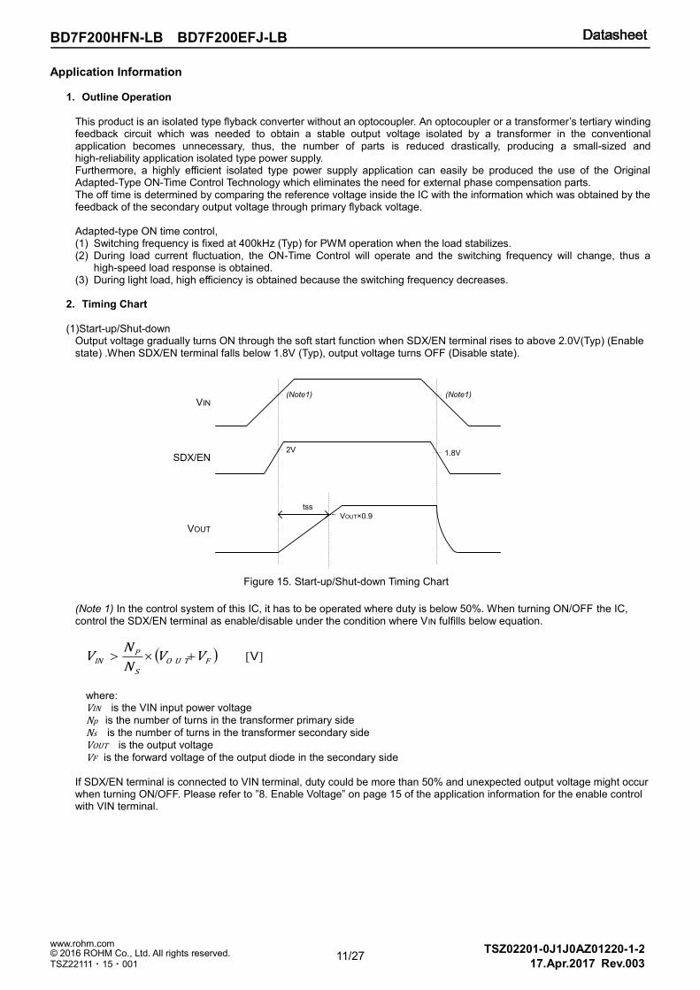
(1)Start-up/Shut-down Output voltage gradually turns ON through the soft start function when SDX/EN terminal rises to above 2.0V(Typ) (Enable state) .When SDX/EN terminal falls below 1.8V (Typ), output voltage turns OFF (Disable state). (Note 1) In the control system of this IC, it has to be operated where duty is below 50%. When turning ON/OFF the IC, control the SDX/EN terminal as enable/disable under the condition where VIN fulfills below equation.
][VFO U T
S
PIN VV
N
NV
where: VIN is the VIN input power voltage Np is the number of turns in the transformer primary side Ns is the number of turns in the transformer secondary side VOUT is the output voltage VF is the forward voltage of the output diode in the secondary side If SDX/EN terminal is connected to VIN terminal, duty could be more than 50% and unexpected output voltage might occur when turning ON/OFF. Please refer to ”8. Enable Voltage” on page 15 of the application information for the enable control with VIN terminal.
VIN
SDX/EN
(Note1) (Note1)
VOUT
2V 1.8V
VOUT×0.9
tss
Figure 15. Start-up/Shut-down Timing Chart
12/27
BD7F200HFN-LB BD7F200EFJ-LB
TSZ02201-0J1J0AZ01220-1-2
© 2016 ROHM Co., Ltd. All rights reserved. 17.Apr.2017 Rev.003
www.rohm.com
TSZ22111・15・001
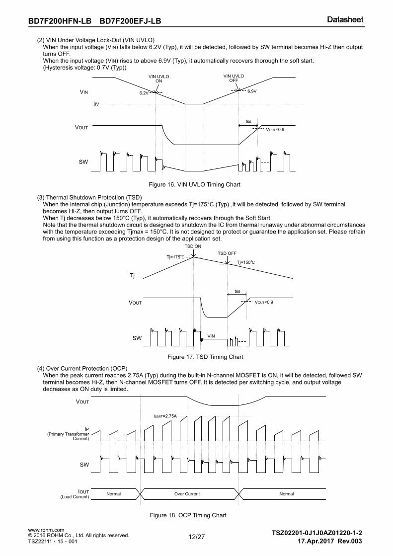
(2) VIN Under Voltage Lock-Out (VIN UVLO) When the input voltage (VIN) falls below 6.2V (Typ), it will be detected, followed by SW terminal becomes Hi-Z then output turns OFF. When the input voltage (VIN) rises to above 6.9V (Typ), it automatically recovers thorough the soft start. (Hysteresis voltage: 0.7V (Typ))
(3) Thermal Shutdown Protection (TSD) When the internal chip (Junction) temperature exceeds Tj=175°C (Typ) ,it will be detected, followed by SW terminal becomes Hi-Z, then output turns OFF. When Tj decreases below 150°C (Typ), it automatically recovers through the Soft Start. Note that the thermal shutdown circuit is designed to shutdown the IC from thermal runaway under abnormal circumstances with the temperature exceeding Tjmax = 150°C. It is not designed to protect or guarantee the application set. Please refrain from using this function as a protection design of the application set.
(4) Over Current Protection (OCP)
When the peak current reaches 2.75A (Typ) during the built-in N-channel MOSFET is ON, it will be detected, followed SW terminal becomes Hi-Z, then N-channel MOSFET turns OFF. It is detected per switching cycle, and output voltage decreases as ON duty is limited.
Figure 17. TSD Timing Chart
Figure 16. VIN UVLO Timing Chart
Figure 18. OCP Timing Chart
VIN
VOUT
SW
VIN UVLOON
VIN UVLOOFF
6.2V 6.9V
tss
VOUT×0.9
0V
SW
VOUT
VIN
Tj=175
Tj
TSD ON
TSD OFF
Tj=150
tss
VOUT×0.9
VOUT
IP(Primary Transformer
Current)
Normal
ILIMIT=2.75A
SW
NormalOver CurrentIOUT(Load Current)
13/27
BD7F200HFN-LB BD7F200EFJ-LB
TSZ02201-0J1J0AZ01220-1-2
© 2016 ROHM Co., Ltd. All rights reserved. 17.Apr.2017 Rev.003
www.rohm.com
TSZ22111・15・001
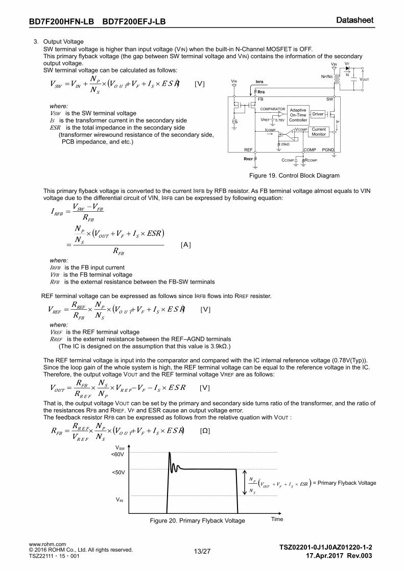
3.Output Voltage
SW terminal voltage is higher than input voltage (VIN) when the built-in N-Channel MOSFET is OFF. This primary flyback voltage (the gap between SW terminal voltage and VIN) contains the information of the secondary output voltage. SW terminal voltage can be calculated as follows:
][VE S RIVVN
NVV SFO U T
S
PINSW
where: VSW is the SW terminal voltage
IS is the transformer current in the secondary side
ESR is the total impedance in the secondary side
(transformer wirewound resistance of the secondary side, PCB impedance, and etc.)
This primary flyback voltage is converted to the current IRFB by RFB resistor. As FB terminal voltage almost equals to VIN voltage due to the differential circuit of VIN, IRFB can be expressed by following equation:
FB
FBSWRFB R
VVI
][A
FB
SFOUT
S
P
R
ESRIVVN
N
where: IRFB is the FB input current VFB is the FB terminal voltage RFB is the external resistance between the FB-SW terminals
REF terminal voltage can be expressed as follows since IRFB flows into RREF resister.
][VE S RIVVN
N
R
RV SFO U T
S
P
FB
REFREF
where: VREF is the REF terminal voltage RREF is the external resistance between the REF–AGND terminals
(The IC is designed on the assumption that this value is 3.9kΩ.) The REF terminal voltage is input into the comparator and compared with the IC internal reference voltage (0.78V(Typ)). Since the loop gain of the whole system is high, the REF terminal voltage can be equal to the reference voltage in the IC. Therefore, the output voltage VOUT and the REF terminal voltage VREF are as follows:
][VE S RIVVN
N
R
RV SFR E F
P
S
R E F
FBOUT
That is, the output voltage VOUT can be set by the primary and secondary side turns ratio of the transformer, and the ratio of the resistances RFB and RREF. VF and ESR cause an output voltage error. The feedback resistor RFB can be expressed as follows from the relative quation with VOUT :
][ΩE S RIVVN
N
V
RR SFO U T
S
P
R E F
R E FFB
Figure 19. Control Block Diagram
COMPARATOR
VF
VOUT
VIN
VIN
Adaptive
On-Time
Controller
RCOMP
IP
NP/NS
ICOMP
0.78V
IS
VREF
VCOMP Current
Monitor
COMPREF
FB SW
PGND
CCOMP
25kΩ
RREF
IRFB
RFB
Driver
VIN
<60V
<50V
VSW
Time
ESRIVV
N
N
SFOUT
S
P
Figure 20. Primary Flyback Voltage
= Primary Flyback Voltage
14/27
BD7F200HFN-LB BD7F200EFJ-LB
TSZ02201-0J1J0AZ01220-1-2
© 2016 ROHM Co., Ltd. All rights reserved. 17.Apr.2017 Rev.003
www.rohm.com
TSZ22111・15・001
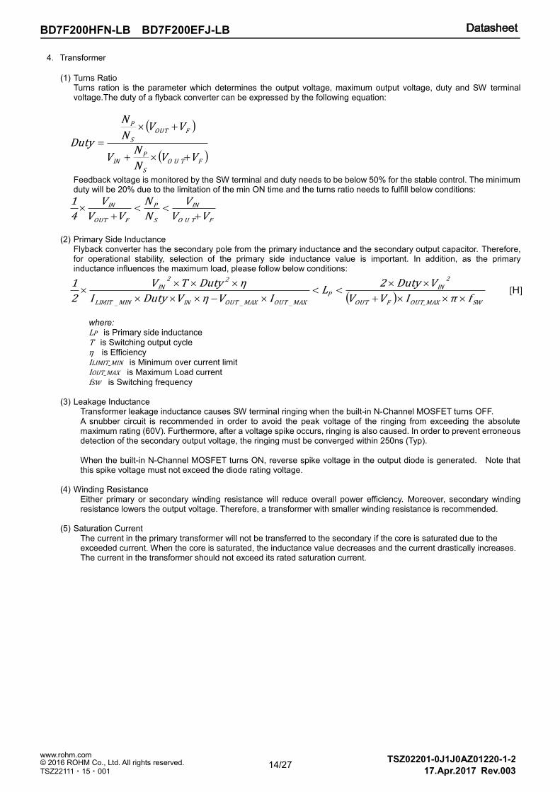
4.Transformer
(1) Turns Ratio
Turns ration is the parameter which determines the output voltage, maximum output voltage, duty and SW terminal voltage.The duty of a flyback converter can be expressed by the following equation:
FO U T
S
PIN
FOUT
S
P
VVN
NV
VVN
N
Duty
Feedback voltage is monitored by the SW terminal and duty needs to be below 50% for the stable control. The minimum duty will be 20% due to the limitation of the min ON time and the turns ratio needs to fulfill below conditions:
FO U T
IN
S
P
FOUT
IN
VV
V
N
N
VV
V
4
1
(2) Primary Side Inductance
Flyback converter has the secondary pole from the primary inductance and the secondary output capacitor. Therefore, for operational stability, selection of the primary side inductance value is important. In addition, as the primary inductance influences the maximum load, please follow below conditions:
][
___
HSWOUT_MAXFOUT
2IN
P
MAXOUTMAXOUTINMINLIMIT
22IN
fπIVV
VDuty2L
IVηVDutyI
ηDutyTV
2
1
where: LP is Primary side inductance
T is Switching output cycle
η is Efficiency
ILIMIT_MIN is Minimum over current limit
IOUT_MAX is Maximum Load current
fSW is Switching frequency
(3) Leakage Inductance
Transformer leakage inductance causes SW terminal ringing when the built-in N-Channel MOSFET turns OFF. A snubber circuit is recommended in order to avoid the peak voltage of the ringing from exceeding the absolute maximum rating (60V). Furthermore, after a voltage spike occurs, ringing is also caused. In order to prevent erroneous detection of the secondary output voltage, the ringing must be converged within 250ns (Typ). When the built-in N-Channel MOSFET turns ON, reverse spike voltage in the output diode is generated. Note that this spike voltage must not exceed the diode rating voltage.
(4) Winding Resistance Either primary or secondary winding resistance will reduce overall power efficiency. Moreover, secondary winding resistance lowers the output voltage. Therefore, a transformer with smaller winding resistance is recommended.
(5) Saturation Current The current in the primary transformer will not be transferred to the secondary if the core is saturated due to the exceeded current. When the core is saturated, the inductance value decreases and the current drastically increases. The current in the transformer should not exceed its rated saturation current.
15/27
BD7F200HFN-LB BD7F200EFJ-LB
TSZ02201-0J1J0AZ01220-1-2
© 2016 ROHM Co., Ltd. All rights reserved. 17.Apr.2017 Rev.003
www.rohm.com
TSZ22111・15・001
5.Output Capacitor
Selecting the secondary side output capacitor value is important for a stable operation. Please select the value which fulfils below condition.
][. F
2
S
P
P
9O U T D u t y
N
N
L
11061C
where:
COUT is Output capacitor
In addition, as secondary side output voltage rises through soft start time (tSS), please consider below equation when choosing an output capacitor. Over current protection operates due to the inrush current especially when the capacitance value is extremely large, thus, start-up failure might occur.
][
__
F
O U T
M A XO U T
S
PM I NL I M I TSS
OUTV
IDuty1N
NIt
2
1C
where: tSS is Soft start time
6.Input Capacitor
Use ceramic capacitor for the input capacitor and place the input capacitor as close as possible to VIN terminal. Please refer to the “PCB Layout Design Guidelines” on page 19 for the design as malfunctions might occur due to the layout pattern or the position of the capacitor. As for the capacitance value of the input capacitor, the ripple voltage of VIN terminal needs to be below 4% of the input voltage. And, make sure that ripple voltage is suppressed when load changes or start up.
7.Output Diode
Since the forward voltage VF of the output diode becomes an error factor in the output voltage, a Schottky barrier diode of small VF is recommended. When selecting a diode, note that forward current must not exceed the rated values. And, when the built-in N-Channel MOSFET is ON, the output diode or reverse voltage VR decrease is expressed by the following equation:
][VO U T
P
SINR V
N
NVV
Furthermore, ringing occurs to the reverse voltage VR when built-in N-Channel MOSFET turns ON. Please prevent the peak voltage from exceeding the rated value of the output diode.
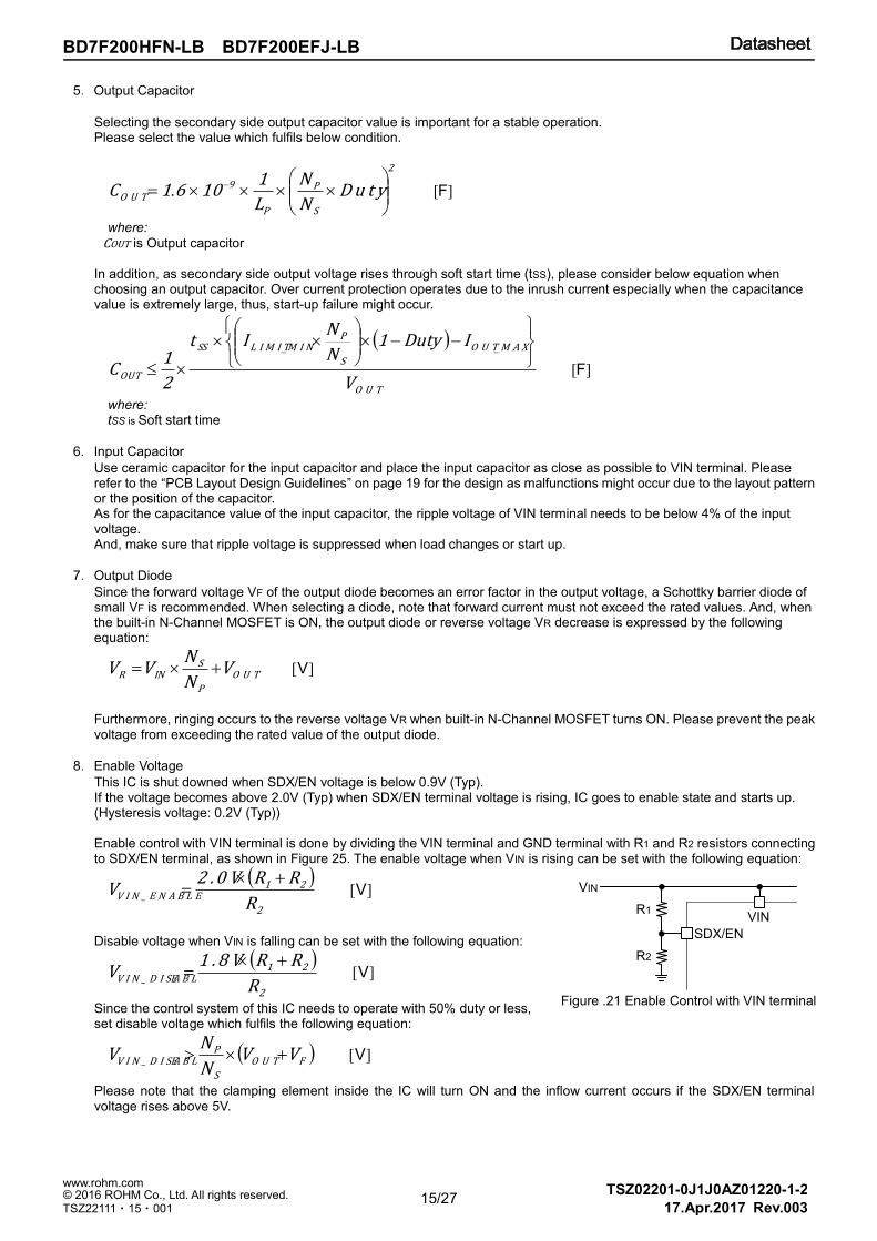
8.Enable Voltage
This IC is shut downed when SDX/EN voltage is below 0.9V (Typ). If the voltage becomes above 2.0V (Typ) when SDX/EN terminal voltage is rising, IC goes to enable state and starts up. (Hysteresis voltage: 0.2V (Typ)) Enable control with VIN terminal is done by dividing the VIN terminal and GND terminal with R1 and R2 resistors connecting to SDX/EN terminal, as shown in Figure 25. The enable voltage when VIN is rising can be set with the following equation:
][V
2
21V I N _ E N A B L E
R
RR2 . 0 VV
Disable voltage when VIN is falling can be set with the following equation:
][V
2
21EV I N _ D I S A B L
R
RR1 . 8 VV
Since the control system of this IC needs to operate with 50% duty or less, set disable voltage which fulfils the following equation:
][VFO U T
S
PEV I N _ D I S A B L VV
N
NV
Please note that the clamping element inside the IC will turn ON and the inflow current occurs if the SDX/EN terminal voltage rises above 5V.
Figure .21 Enable Control with VIN terminal
VIN
SDX/EN
VIN
R1
R2
16/27
BD7F200HFN-LB BD7F200EFJ-LB
TSZ02201-0J1J0AZ01220-1-2
© 2016 ROHM Co., Ltd. All rights reserved. 17.Apr.2017 Rev.003
www.rohm.com
TSZ22111・15・001
9.Minimum Load Current
To achieve a stable output voltage, the built-in N-Channel MOSFET senses and feeds back information on the output voltage on the secondary side (which was isolated by the transformer) by using the SW terminal voltage on the primary side (during OFF time). Meaning, the output will not be regulated in any case unless the built-in N-Channel MOSFET is in the switching operation. During light load, the switching operation uses minimum ON-Time. The output voltage may rise when there is a small load current since it will supply the least amount of energy to the secondary side output. Therefore, it is necessary to add a dummy resistor etc. to the output in order to secure minimum load current. The required minimum load current (IOUT_MIN) can be expressed by:
][A
O U TP
2
IN9OUT_MIN VL
V105.7I
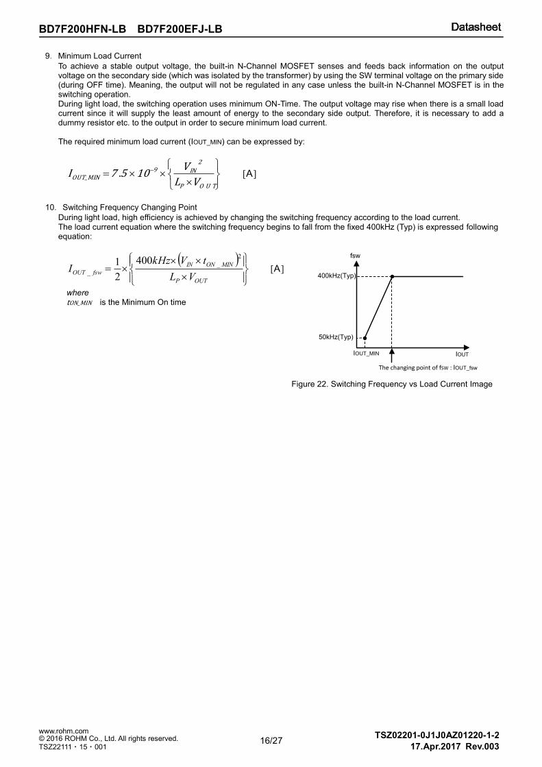
10.Switching Frequency Changing Point
During light load, high efficiency is achieved by changing the switching frequency according to the load current. The load current equation where the switching frequency begins to fall from the fixed 400kHz (Typ) is expressed following equation:
][
2
_
_
400
2
1A
OUTP
MINONIN
fswOUTVL
tVkHzI
where tON_MIN is the Minimum On time
Figure 22. Switching Frequency vs Load Current Image
fsw
IOUTIOUT_MIN
The changing point of fSW : IOUT_fsw
400kHz(Typ)
50kHz(Typ)
17/27
BD7F200HFN-LB BD7F200EFJ-LB
TSZ02201-0J1J0AZ01220-1-2
© 2016 ROHM Co., Ltd. All rights reserved. 17.Apr.2017 Rev.003
www.rohm.com
TSZ22111・15・001
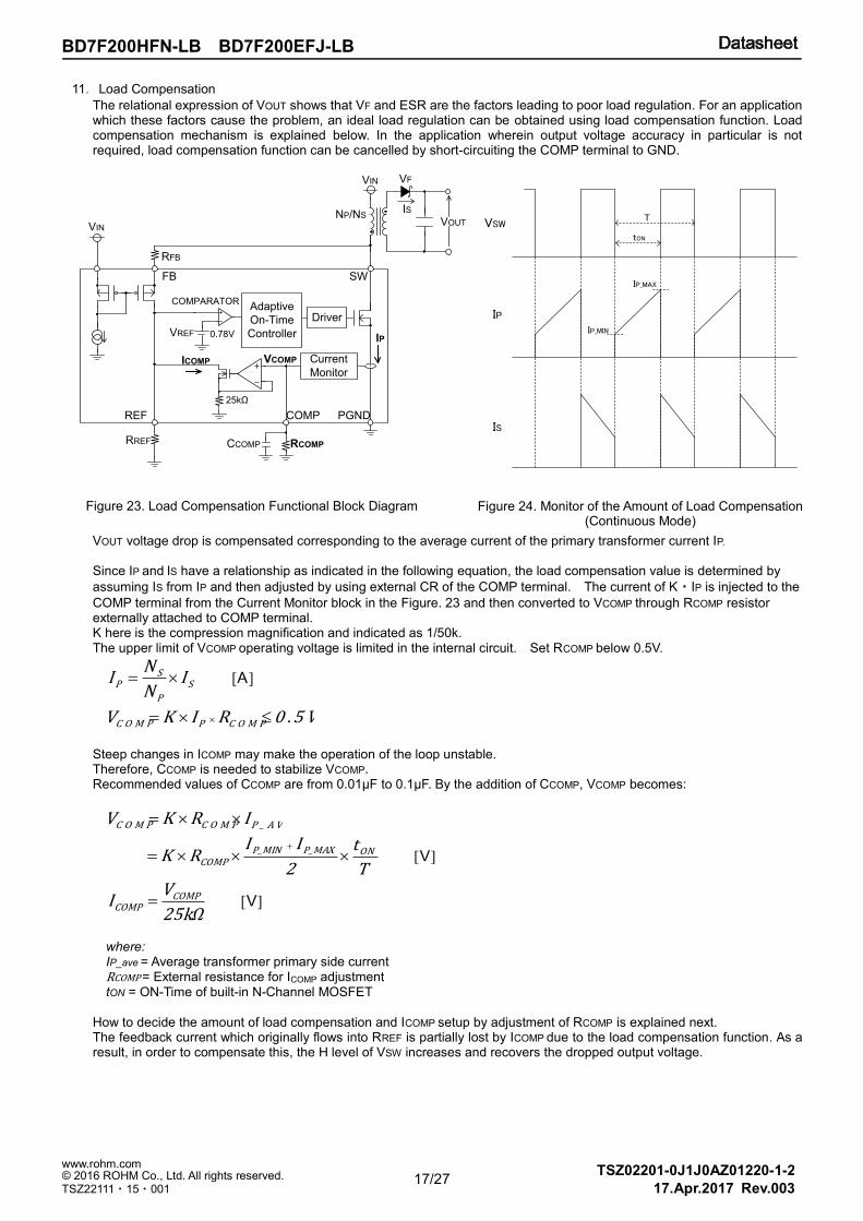
11.Load Compensation
The relational expression of VOUT shows that VF and ESR are the factors leading to poor load regulation. For an application which these factors cause the problem, an ideal load regulation can be obtained using load compensation function. Load compensation mechanism is explained below. In the application wherein output voltage accuracy in particular is not required, load compensation function can be cancelled by short-circuiting the COMP terminal to GND.
VOUT voltage drop is compensated corresponding to the average current of the primary transformer current IP. Since IP and IS have a relationship as indicated in the following equation, the load compensation value is determined by
assuming IS from IP and then adjusted by using external CR of the COMP terminal. The current of K・IP is injected to the
COMP terminal from the Current Monitor block in the Figure. 23 and then converted to VCOMP through RCOMP resistor externally attached to COMP terminal. K here is the compression magnification and indicated as 1/50k. The upper limit of VCOMP operating voltage is limited in the internal circuit. Set RCOMP below 0.5V.
][AS
P
SP I
N
NI
0 . 5 VRIKV C O M PPC O M P
Steep changes in ICOMP may make the operation of the loop unstable. Therefore, CCOMP is needed to stabilize VCOMP. Recommended values of CCOMP are from 0.01µF to 0.1µF. By the addition of CCOMP, VCOMP becomes:
P _ A V EC O M PC O M P IRKV
][VT
t
2
IIRK ONP_MAXP_MIN
COMP
][VΩ25k
VI COMP
COMP
where: IP_ave = Average transformer primary side current RCOMP = External resistance for ICOMP adjustment tON = ON-Time of built-in N-Channel MOSFET How to decide the amount of load compensation and ICOMP setup by adjustment of RCOMP is explained next. The feedback current which originally flows into RREF is partially lost by ICOMP due to the load compensation function. As a result, in order to compensate this, the H level of VSW increases and recovers the dropped output voltage.
Figure 23. Load Compensation Functional Block Diagram Figure 24. Monitor of the Amount of Load Compensation (Continuous Mode)
VSW
IPIP_MIN
IP_MAX
T
tON
IS
COMPARATOR
VF
VOUT
VIN
VIN
Adaptive
On-Time
Controller
RCOMP
IP
NP/NS
ICOMP
0.78V
IS
VREF
VCOMP Current
Monitor
COMPREF
FB SW
PGND
CCOMP
25kΩ
RREF
RFB
Driver
18/27
BD7F200HFN-LB BD7F200EFJ-LB
TSZ02201-0J1J0AZ01220-1-2
© 2016 ROHM Co., Ltd. All rights reserved. 17.Apr.2017 Rev.003
www.rohm.com
TSZ22111・15・001
While the load compensation function is not operating, VOUT, as described previously, will now be:
][VE S RIVVN
N
R
RV S _ A V EFR E F
P
S
R E F
FBOUT
where: IS_AVE is the average transformer secondary side current When ICOMP occurs, the load compensation function operates and VOUT becomes the following equation. The voltage VOUT increases by ICOMP.
][VE S RIVR)IR
V(
N
NV S _ A V EFFBCOMP
REF
REF
P
SOUT
E S RIRIRN
N
25kΩ
IRKS_AVEVFS_AVEFB
P
SAVEPCOMP
_
In order to remove VF and ESR by using ICOMP, the following equation is needed.
E S RIVRN
NI S _ A V EFFB
P
SCOMP
Next, linearity approximation of the change of VF to IS is carried out by RVF, and RCOMP which adjusts ICOMP from the expression mentioned earlier is calculated.
E S RIRIRN
N
25kΩ
IRKS_AVEVFS_AVEFB
P
SP_AVECOMP
E S RRRN
N
25kΩ
RKVFFB
2
P
SCOMP
][Ω
2
S
P
FB
VFCOMP
N
N
RK
ESRR25kR Ω
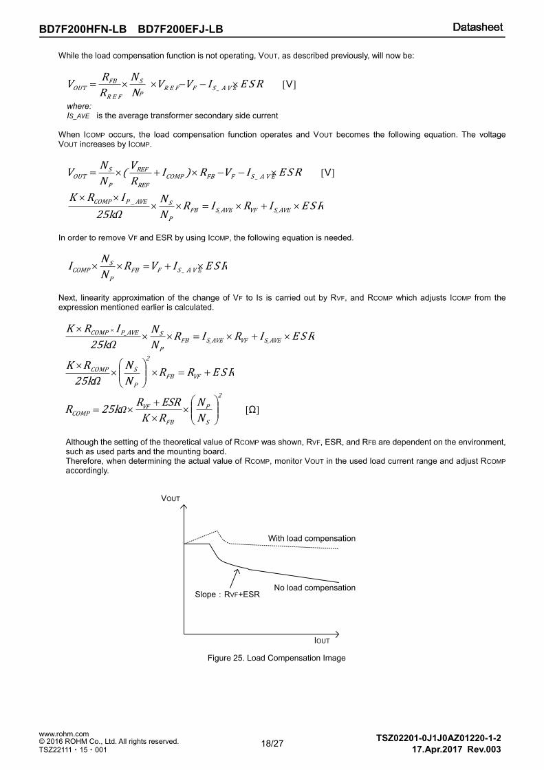
Although the setting of the theoretical value of RCOMP was shown, RVF, ESR, and RFB are dependent on the environment, such as used parts and the mounting board. Therefore, when determining the actual value of RCOMP, monitor VOUT in the used load current range and adjust RCOMP accordingly.
VOUT
IOUT
With load compensation
No load compensationSlope:RVF+ESR
Figure 25. Load Compensation Image
19/27
BD7F200HFN-LB BD7F200EFJ-LB
TSZ02201-0J1J0AZ01220-1-2
© 2016 ROHM Co., Ltd. All rights reserved. 17.Apr.2017 Rev.003
www.rohm.com
TSZ22111・15・001
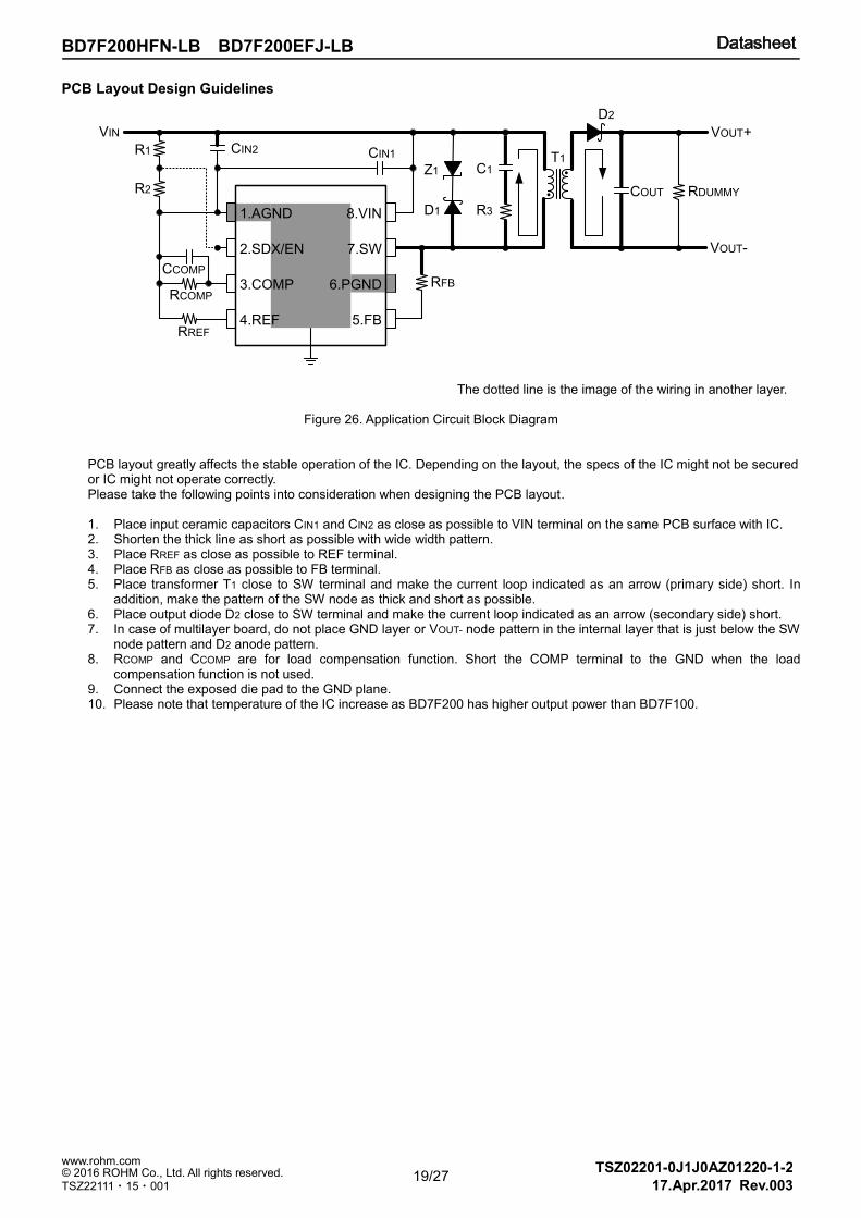
PCB Layout Design Guidelines
The dotted line is the image of the wiring in another layer.
Figure 26. Application Circuit Block Diagram
PCB layout greatly affects the stable operation of the IC. Depending on the layout, the specs of the IC might not be secured or IC might not operate correctly. Please take the following points into consideration when designing the PCB layout.
1. Place input ceramic capacitors CIN1 and CIN2 as close as possible to VIN terminal on the same PCB surface with IC. 2. Shorten the thick line as short as possible with wide width pattern. 3. Place RREF as close as possible to REF terminal. 4. Place RFB as close as possible to FB terminal. 5. Place transformer T1 close to SW terminal and make the current loop indicated as an arrow (primary side) short. In
addition, make the pattern of the SW node as thick and short as possible. 6. Place output diode D2 close to SW terminal and make the current loop indicated as an arrow (secondary side) short. 7. In case of multilayer board, do not place GND layer or VOUT- node pattern in the internal layer that is just below the SW
node pattern and D2 anode pattern. 8. RCOMP and CCOMP are for load compensation function. Short the COMP terminal to the GND when the load
compensation function is not used. 9. Connect the exposed die pad to the GND plane. 10. Please note that temperature of the IC increase as BD7F200 has higher output power than BD7F100.
VOUT+
VOUT-
VIN
COUT
D2
D1
Z1T1
C1
R3
RDUMMY
RREF
RCOMP
CCOMP
R1
R2
CIN2 CIN1
RFB
1.AGND
2.SDX/EN
3.COMP
4.REF 5.FB
6.PGND
7.SW
8.VIN
20/27
BD7F200HFN-LB BD7F200EFJ-LB
TSZ02201-0J1J0AZ01220-1-2
© 2016 ROHM Co., Ltd. All rights reserved. 17.Apr.2017 Rev.003
www.rohm.com
TSZ22111・15・001
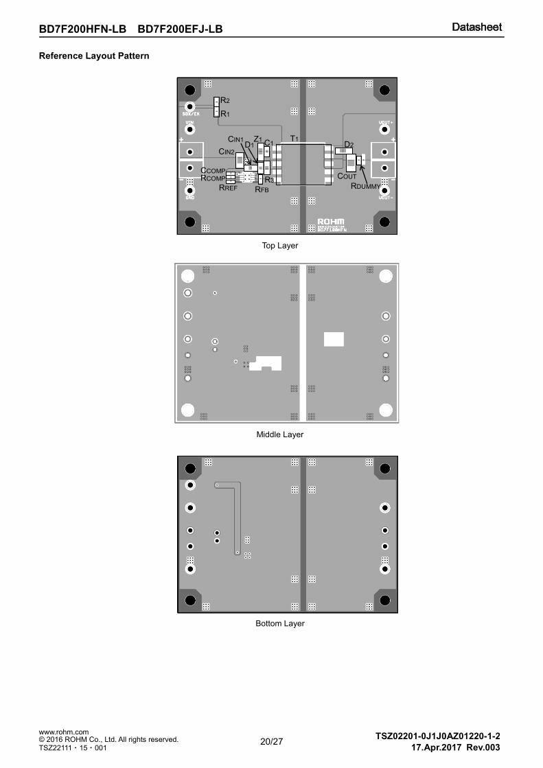
Reference Layout Pattern
Top Layer
Middle Layer
Bottom Layer
RFB
R3
CIN1 D1 C1
CIN2
CCOMP RCOMP
RREF
R2
R1
T1 D2
RDUMMY
COUT
Z1
21/27
BD7F200HFN-LB BD7F200EFJ-LB
TSZ02201-0J1J0AZ01220-1-2
© 2016 ROHM Co., Ltd. All rights reserved. 17.Apr.2017 Rev.003
www.rohm.com
TSZ22111・15・001
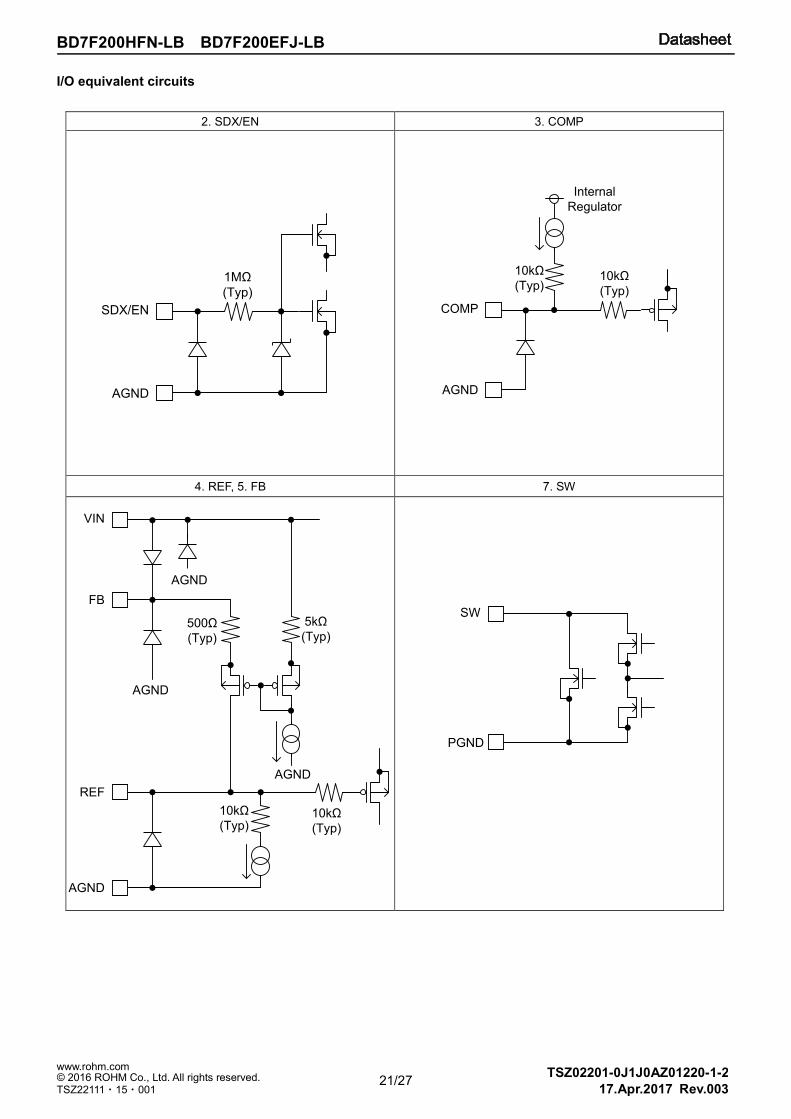
I/O equivalent circuits
2. SDX/EN 3. COMP
4. REF, 5. FB 7. SW
SDX/EN
AGND
1MΩ
(Typ)
COMP
10kΩ
(Typ)
Internal
Regulator
10kΩ
(Typ)
AGND
SW
PGND
VIN
FB
AGND
500Ω
(Typ)
AGND
5kΩ
(Typ)
REF
AGND
10kΩ
(Typ)10kΩ
(Typ)
AGND
22/27
BD7F200HFN-LB BD7F200EFJ-LB
TSZ02201-0J1J0AZ01220-1-2
© 2016 ROHM Co., Ltd. All rights reserved. 17.Apr.2017 Rev.003
www.rohm.com
TSZ22111・15・001
Operational Notes
1. Reverse Connection of Power Supply
Connecting the power supply in reverse polarity can damage the IC. Take precautions against reverse polarity when connecting the power supply, such as mounting an external diode between the power supply and the IC’s power supply pins.
2. Power Supply Lines
Design the PCB layout pattern to provide low impedance supply lines. Furthermore, connect a capacitor to ground at all power supply pins. Consider the effect of temperature and aging on the capacitance value when using electrolytic capacitors.
3. Ground Voltage
Ensure that no pins are at a voltage below that of the ground pin at any time, even during transient condition.
4. Ground Wiring Pattern
When using both small-signal and large-current ground traces, the two ground traces should be routed separately but connected to a single ground at the reference point of the application board to avoid fluctuations in the small-signal ground caused by large currents. Also ensure that the ground traces of external components do not cause variations on the ground voltage. The ground lines must be as short and thick as possible to reduce line impedance.
5. Thermal Consideration
Should by any chance the power dissipation rating be exceeded the rise in temperature of the chip may result in deterioration of the properties of the chip. In case of exceeding this absolute maximum rating, increase the board size and copper area to prevent exceeding the Pd rating.
6. Recommended Operating Conditions
These conditions represent a range within which the expected characteristics of the IC can be approximately obtained. The electrical characteristics are guaranteed under the conditions of each parameter.
7. Inrush Current
When power is first supplied to the IC, it is possible that the internal logic may be unstable and inrush current may flow instantaneously due to the internal powering sequence and delays, especially if the IC has more than one power supply. Therefore, give special consideration to power coupling capacitance, power wiring, width of ground wiring, and routing of connections.
8. Operation Under Strong Electromagnetic Field
Operating the IC in the presence of a strong electromagnetic field may cause the IC to malfunction.
9. Testing on Application Boards
When testing the IC on an application board, connecting a capacitor directly to a low-impedance output pin may subject the IC to stress. Always discharge capacitors completely after each process or step. The IC’s power supply should always be turned off completely before connecting or removing it from the test setup during the inspection process. To prevent damage from static discharge, ground the IC during assembly and use similar precautions during transport and storage.
10. Inter-pin Short and Mounting Errors
Ensure that the direction and position are correct when mounting the IC on the PCB. Incorrect mounting may result in damaging the IC. Avoid nearby pins being shorted to each other especially to ground, power supply and output pin. Inter-pin shorts could be due to many reasons such as metal particles, water droplets (in very humid environment) and unintentional solder bridge deposited in between pins during assembly to name a few.
11. Unused Input Pins
Input pins of an IC are often connected to the gate of a MOS transistor. The gate has extremely high impedance and extremely low capacitance. If left unconnected, the electric field from the outside can easily charge it. The small charge acquired in this way is enough to produce a significant effect on the conduction through the transistor and cause unexpected operation of the IC. So unless otherwise specified, unused input pins should be connected to the power supply or ground line.
23/27
BD7F200HFN-LB BD7F200EFJ-LB
TSZ02201-0J1J0AZ01220-1-2
© 2016 ROHM Co., Ltd. All rights reserved. 17.Apr.2017 Rev.003
www.rohm.com
TSZ22111・15・001
Operational Notes – continued
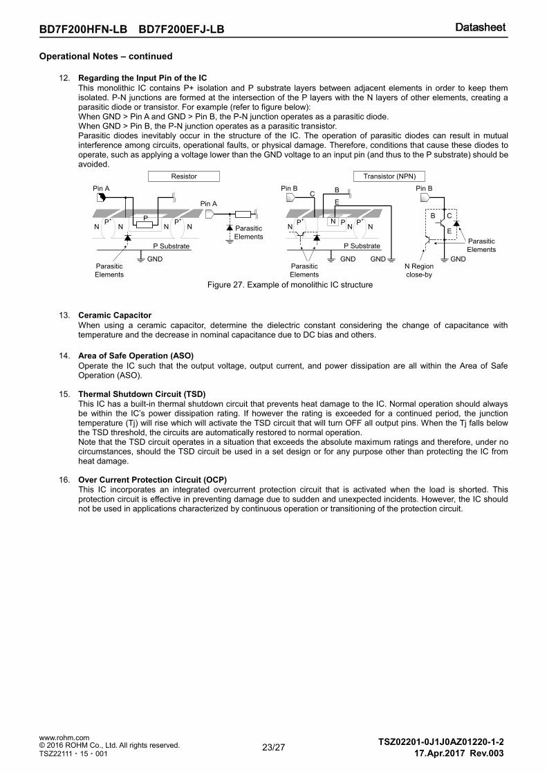
12. Regarding the Input Pin of the IC
This monolithic IC contains P+ isolation and P substrate layers between adjacent elements in order to keep them isolated. P-N junctions are formed at the intersection of the P layers with the N layers of other elements, creating a parasitic diode or transistor. For example (refer to figure below): When GND > Pin A and GND > Pin B, the P-N junction operates as a parasitic diode. When GND > Pin B, the P-N junction operates as a parasitic transistor. Parasitic diodes inevitably occur in the structure of the IC. The operation of parasitic diodes can result in mutual interference among circuits, operational faults, or physical damage. Therefore, conditions that cause these diodes to operate, such as applying a voltage lower than the GND voltage to an input pin (and thus to the P substrate) should be avoided.
Figure 27. Example of monolithic IC structure
13. Ceramic Capacitor
When using a ceramic capacitor, determine the dielectric constant considering the change of capacitance with temperature and the decrease in nominal capacitance due to DC bias and others.
14. Area of Safe Operation (ASO)
Operate the IC such that the output voltage, output current, and power dissipation are all within the Area of Safe Operation (ASO).
15. Thermal Shutdown Circuit (TSD)
This IC has a built-in thermal shutdown circuit that prevents heat damage to the IC. Normal operation should always be within the IC’s power dissipation rating. If however the rating is exceeded for a continued period, the junction temperature (Tj) will rise which will activate the TSD circuit that will turn OFF all output pins. When the Tj falls below the TSD threshold, the circuits are automatically restored to normal operation. Note that the TSD circuit operates in a situation that exceeds the absolute maximum ratings and therefore, under no circumstances, should the TSD circuit be used in a set design or for any purpose other than protecting the IC from heat damage.
16. Over Current Protection Circuit (OCP)
This IC incorporates an integrated overcurrent protection circuit that is activated when the load is shorted. This protection circuit is effective in preventing damage due to sudden and unexpected incidents. However, the IC should not be used in applications characterized by continuous operation or transitioning of the protection circuit.
N NP
+ P
N NP
+
P Substrate
GND
NP
+
N NP
+N P
P Substrate
GND GND
Parasitic
Elements
Pin A
Pin A
Pin B Pin B
B C
E
Parasitic
Elements
GNDParasitic
Elements
CB
E
Transistor (NPN)Resistor
N Region
close-by
Parasitic
Elements
24/27
BD7F200HFN-LB BD7F200EFJ-LB
TSZ02201-0J1J0AZ01220-1-2
© 2016 ROHM Co., Ltd. All rights reserved. 17.Apr.2017 Rev.003
www.rohm.com
TSZ22111・15・001
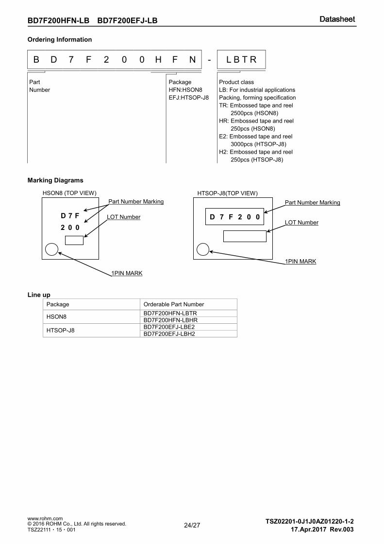
Ordering Information
B D 7 F 2 0 0 H F N - L B T R
Part
Number
Package
HFN:HSON8
EFJ:HTSOP-J8
Product class
LB: For industrial applications
Packing, forming specification
TR: Embossed tape and reel
2500pcs (HSON8)
HR: Embossed tape and reel
250pcs (HSON8)
E2: Embossed tape and reel
3000pcs (HTSOP-J8)
H2: Embossed tape and reel
250pcs (HTSOP-J8)
Marking Diagrams
Line up
Package Orderable Part Number
HSON8 BD7F200HFN-LBTR
BD7F200HFN-LBHR
HTSOP-J8 BD7F200EFJ-LBE2
BD7F200EFJ-LBH2
HSON8 (TOP VIEW)
2 0 0
Part Number Marking
LOT Number
1PIN MARK
D 7 F
HTSOP-J8(TOP VIEW)
D 7 F 2 0 0
Part Number Marking
LOT Number
1PIN MARK
25/27
BD7F200HFN-LB BD7F200EFJ-LB
TSZ02201-0J1J0AZ01220-1-2
© 2016 ROHM Co., Ltd. All rights reserved. 17.Apr.2017 Rev.003
www.rohm.com
TSZ22111・15・001
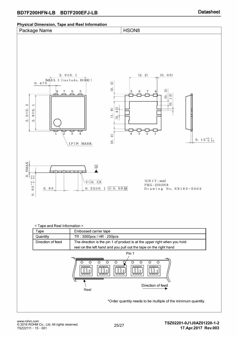
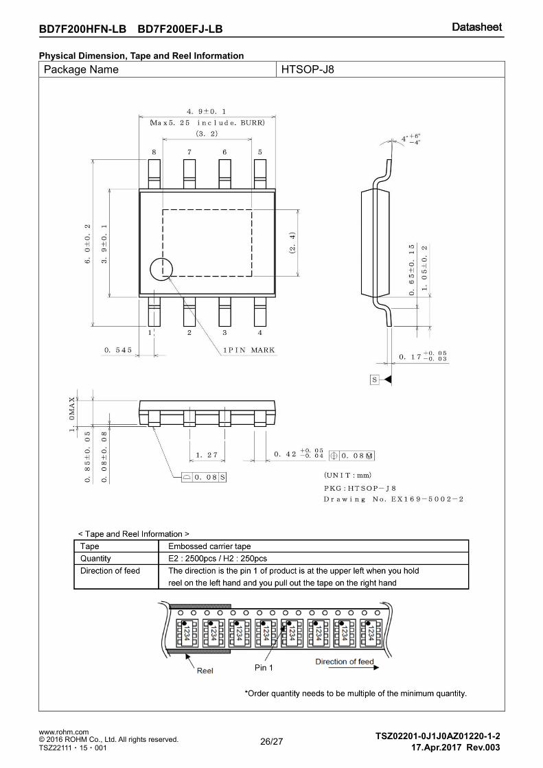
Physical Dimension, Tape and Reel Information
Package Name HSON8
26/27
BD7F200HFN-LB BD7F200EFJ-LB
TSZ02201-0J1J0AZ01220-1-2
© 2016 ROHM Co., Ltd. All rights reserved. 17.Apr.2017 Rev.003
www.rohm.com
TSZ22111・15・001
Physical Dimension, Tape and Reel Information
Package Name HTSOP-J8

27/27
BD7F200HFN-LB BD7F200EFJ-LB
TSZ02201-0J1J0AZ01220-1-2
© 2016 ROHM Co., Ltd. All rights reserved. 17.Apr.2017 Rev.003
www.rohm.com
TSZ22111・15・001
Revision History
Date Revision Changes
10.Mar.2016 001 New production
24.Mar.2016 002 Add BD7F200EFJ-LB(HTSOP-J8 Package)
17.April.2017 003 P.4 Modified FB terminal absolute voltage P.24 Add small lots format P.25 P.26 Add small lots format

Notice-PAA-E Rev.003
© 2015 ROHM Co., Ltd. All rights reserved.
Notice
Precaution on using ROHM Products 1. If you intend to use our Products in devices requiring extremely high reliability (such as medical equipment
(Note 1),
aircraft/spacecraft, nuclear power controllers, etc.) and whose malfunction or failure may cause loss of human life, bodily injury or serious damage to property (“Specific Applications”), please consult with the ROHM sales representative in advance. Unless otherwise agreed in writing by ROHM in advance, ROHM shall not be in any way responsible or liable for any damages, expenses or losses incurred by you or third parties arising from the use of any ROHM’s Products for Specific Applications.
(Note1) Medical Equipment Classification of the Specific Applications
JAPAN USA EU CHINA
CLASSⅢ CLASSⅢ
CLASSⅡb CLASSⅢ
CLASSⅣ CLASSⅢ
2. ROHM designs and manufactures its Products subject to strict quality control system. However, semiconductor
products can fail or malfunction at a certain rate. Please be sure to implement, at your own responsibilities, adequate safety measures including but not limited to fail-safe design against the physical injury, damage to any property, which a failure or malfunction of our Products may cause. The following are examples of safety measures:
[a] Installation of protection circuits or other protective devices to improve system safety [b] Installation of redundant circuits to reduce the impact of single or multiple circuit failure
3. Our Products are not designed under any special or extraordinary environments or conditions, as exemplified below. Accordingly, ROHM shall not be in any way responsible or liable for any damages, expenses or losses arising from the use of any ROHM’s Products under any special or extraordinary environments or conditions. If you intend to use our Products under any special or extraordinary environments or conditions (as exemplified below), your independent verification and confirmation of product performance, reliability, etc, prior to use, must be necessary:
[a] Use of our Products in any types of liquid, including water, oils, chemicals, and organic solvents [b] Use of our Products outdoors or in places where the Products are exposed to direct sunlight or dust [c] Use of our Products in places where the Products are exposed to sea wind or corrosive gases, including Cl2,
H2S, NH3, SO2, and NO2
[d] Use of our Products in places where the Products are exposed to static electricity or electromagnetic waves [e] Use of our Products in proximity to heat-producing components, plastic cords, or other flammable items [f] Sealing or coating our Products with resin or other coating materials [g] Use of our Products without cleaning residue of flux (even if you use no-clean type fluxes, cleaning residue of
flux is recommended); or Washing our Products by using water or water-soluble cleaning agents for cleaning residue after soldering
[h] Use of the Products in places subject to dew condensation
4. The Products are not subject to radiation-proof design. 5. Please verify and confirm characteristics of the final or mounted products in using the Products. 6. In particular, if a transient load (a large amount of load applied in a short period of time, such as pulse. is applied,
confirmation of performance characteristics after on-board mounting is strongly recommended. Avoid applying power exceeding normal rated power; exceeding the power rating under steady-state loading condition may negatively affect product performance and reliability.
7. De-rate Power Dissipation depending on ambient temperature. When used in sealed area, confirm that it is the use in
the range that does not exceed the maximum junction temperature. 8. Confirm that operation temperature is within the specified range described in the product specification. 9. ROHM shall not be in any way responsible or liable for failure induced under deviant condition from what is defined in
this document.
Precaution for Mounting / Circuit board design 1. When a highly active halogenous (chlorine, bromine, etc.) flux is used, the residue of flux may negatively affect product
performance and reliability. 2. In principle, the reflow soldering method must be used on a surface-mount products, the flow soldering method must
be used on a through hole mount products. If the flow soldering method is preferred on a surface-mount products, please consult with the ROHM representative in advance.
For details, please refer to ROHM Mounting specification

Notice-PAA-E Rev.003
© 2015 ROHM Co., Ltd. All rights reserved.
Precautions Regarding Application Examples and External Circuits 1. If change is made to the constant of an external circuit, please allow a sufficient margin considering variations of the
characteristics of the Products and external components, including transient characteristics, as well as static characteristics.
2. You agree that application notes, reference designs, and associated data and information contained in this document
are presented only as guidance for Products use. Therefore, in case you use such information, you are solely responsible for it and you must exercise your own independent verification and judgment in the use of such information contained in this document. ROHM shall not be in any way responsible or liable for any damages, expenses or losses incurred by you or third parties arising from the use of such information.
Precaution for Electrostatic This Product is electrostatic sensitive product, which may be damaged due to electrostatic discharge. Please take proper caution in your manufacturing process and storage so that voltage exceeding the Products maximum rating will not be applied to Products. Please take special care under dry condition (e.g. Grounding of human body / equipment / solder iron, isolation from charged objects, setting of Ionizer, friction prevention and temperature / humidity control).
Precaution for Storage / Transportation 1. Product performance and soldered connections may deteriorate if the Products are stored in the places where:
[a] the Products are exposed to sea winds or corrosive gases, including Cl2, H2S, NH3, SO2, and NO2 [b] the temperature or humidity exceeds those recommended by ROHM [c] the Products are exposed to direct sunshine or condensation [d] the Products are exposed to high Electrostatic
2. Even under ROHM recommended storage condition, solderability of products out of recommended storage time period may be degraded. It is strongly recommended to confirm solderability before using Products of which storage time is exceeding the recommended storage time period.
3. Store / transport cartons in the correct direction, which is indicated on a carton with a symbol. Otherwise bent leads
may occur due to excessive stress applied when dropping of a carton. 4. Use Products within the specified time after opening a humidity barrier bag. Baking is required before using Products of
which storage time is exceeding the recommended storage time period.
Precaution for Product Label A two-dimensional barcode printed on ROHM Products label is for ROHM’s internal use only.
Precaution for Disposition When disposing Products please dispose them properly using an authorized industry waste company.
Precaution for Foreign Exchange and Foreign Trade act Since concerned goods might be fallen under listed items of export control prescribed by Foreign exchange and Foreign trade act, please consult with ROHM in case of export.
Precaution Regarding Intellectual Property Rights 1. All information and data including but not limited to application example contained in this document is for reference
only. ROHM does not warrant that foregoing information or data will not infringe any intellectual property rights or any other rights of any third party regarding such information or data.
2. ROHM shall not have any obligations where the claims, actions or demands arising from the combination of the Products with other articles such as components, circuits, systems or external equipment (including software).
3. No license, expressly or implied, is granted hereby under any intellectual property rights or other rights of ROHM or any third parties with respect to the Products or the information contained in this document. Provided, however, that ROHM will not assert its intellectual property rights or other rights against you or your customers to the extent necessary to manufacture or sell products containing the Products, subject to the terms and conditions herein.
Other Precaution 1. This document may not be reprinted or reproduced, in whole or in part, without prior written consent of ROHM.
2. The Products may not be disassembled, converted, modified, reproduced or otherwise changed without prior written consent of ROHM.
3. In no event shall you use in any way whatsoever the Products and the related technical information contained in the Products or this document for any military purposes, including but not limited to, the development of mass-destruction weapons.
4. The proper names of companies or products described in this document are trademarks or registered trademarks of ROHM, its affiliated companies or third parties.

DatasheetDatasheet
Notice – WE Rev.001© 2015 ROHM Co., Ltd. All rights reserved.
General Precaution 1. Before you use our Pro ducts, you are requested to care fully read this document and fully understand its contents.
ROHM shall n ot be in an y way responsible or liabl e for fa ilure, malfunction or acci dent arising from the use of a ny ROHM’s Products against warning, caution or note contained in this document.
2. All information contained in this docume nt is current as of the issuing date and subj ect to change without any prior
notice. Before purchasing or using ROHM’s Products, please confirm the la test information with a ROHM sale s representative.
3. The information contained in this doc ument is provi ded on an “as is” basis and ROHM does not warrant that all
information contained in this document is accurate an d/or error-free. ROHM shall not be in an y way responsible or liable for any damages, expenses or losses incurred by you or third parties resulting from inaccuracy or errors of or concerning such information.