isolated switching regulator with integrated feedback data ... · isolated switching regulator with...
TRANSCRIPT
Isolated Switching Regulator With Integrated Feedback
Data Sheet ADuM3070 FEATURES Isolated PWM feedback with built in compensation Primary side transformer driver for up to 2.5 W output power
with 5 V input voltage Regulated adjustable output: 3.3 V to 24 V Up to 80% efficiency 200 kHz to 1 MHz adjustable oscillator Soft start function at power-up Pulse-by-pulse overcurrent protection Thermal shutdown 2500 V rms isolation High common-mode transient immunity: >25 kV/µs 16-lead QSOP package High temperature operation: 105°C
APPLICATIONS Power supply startup bias and gate drives Isolated sensor interfaces Process controls
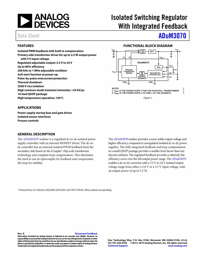
FUNCTIONAL BLOCK DIAGRAM
Figure 1.
GENERAL DESCRIPTION The ADuM30701 isolator is a regulated dc-to-dc isolated power supply controller with an internal MOSFET driver. The dc-to-dc controller has an internal isolated PWM feedback from the secondary side based on the iCoupler® chip scale transformer technology and complete loop compensation. This eliminates the need to use an optocoupler for feedback and compensates the loop for stability.
The ADuM3070 isolator provides a more stable output voltage and higher efficiency compared to unregulated isolated dc-to-dc power supplies. The fully integrated feedback and loop compensation in a small QSOP package provides a smaller form factor than any discrete solution. The regulated feedback provides a relatively flat efficiency curve over the full output power range. The ADuM3070 enables a dc-to-dc converter with a 3.3 V to 24 V isolated output voltage range from either a 5.0 V or a 3.3 V input voltage, with an output power of up to 2.5 W.
1 Protected by U.S. Patents 5,952,849; 6,873,065; and 7075 329 B2. Other patents are pending.
ADuM3070
1043
7-00
1
PRIMARYCONVERTER/
DRIVER SECONDARYCONTROLLER
INTERNALFEEDBACK
VDD2
OC
FB
VREG
VDD1 VISO
VDDA
X2X1
GND1 GND2
REG
RECT
5V
NOTES1. VDD1 IS THE POWER SUPPLY FOR THE PUSH-PULL TRANSFORMER.2. VDDA IS THE POWER SUPPLY OF SIDE 1 OF THE ADuM3070.
Rev. A Document Feedback Information furnished by Analog Devices is believed to be accurate and reliable. However, no responsibility is assumed by Analog Devices for its use, nor for any infringements of patents or other rights of third parties that may result from its use. Specifications subject to change without notice. No license is granted by implication or otherwise under any patent or patent rights of Analog Devices. Trademarks and registered trademarks are the property of their respective owners.
One Technology Way, P.O. Box 9106, Norwood, MA 02062-9106, U.S.A. Tel: 781.329.4700 ©2012–2014 Analog Devices, Inc. All rights reserved. Technical Support www.analog.com

ADuM3070 Data Sheet
TABLE OF CONTENTS Features .............................................................................................. 1 Applications ....................................................................................... 1 Functional Block Diagram .............................................................. 1 General Description ......................................................................... 1 Revision History ............................................................................... 2 Specifications ..................................................................................... 3
Electrical Characteristics—5 V Primary Input Supply/5 V Secondary Isolated Supply .......................................................... 3 Electrical Characteristics—3.3 V Primary Input Supply/3.3 V Secondary Isolated Supply .......................................................... 3 Electrical Characteristics—5 V Primary Input Supply/3.3 V Secondary Isolated Supply .......................................................... 4 Electrical Characteristics—5 V Primary Input Supply/15 V Secondary Isolated Supply .......................................................... 4 Package Characteristics ............................................................... 5 Regulatory Approvals (Pending) ................................................ 5 Insulation and Safety Related Specifications ............................ 5 DIN V VDE V 0884-10 (VDE V 0884-10) Insulation Characteristics .............................................................................. 6 Recommended Operating Conditions ...................................... 6
Absolute Maximum Ratings ............................................................ 7 ESD Caution .................................................................................. 7
Pin Configuration and Function Descriptions ..............................8 Typical Performance Characteristics ..............................................9 Applications Information .............................................................. 14
Application Schematics ............................................................. 14 Transformer Design ................................................................... 15 Transformer Turns Ratio ........................................................... 15 Transformer ET Constant ......................................................... 15 Transformer Primary Inductance and Resistance ................. 15 Transformer Isolation Voltage .................................................. 16 Switching Frequency .................................................................. 16 Transient Response .................................................................... 16 Component Selection ................................................................ 16 Printed Circuit Board (PCB) Layout ....................................... 17 Thermal Analysis ....................................................................... 17 Power Consumption .................................................................. 17 Power Considerations ................................................................ 18 Insulation Lifetime ..................................................................... 18
Outline Dimensions ....................................................................... 19 Ordering Guide .......................................................................... 19
REVISION HISTORY 5/14—Rev. 0 to Rev. A Change to Line Regulation Parameter, Table 4 ............................. 4 5/12—Revision 0: Initial Version
Rev. A | Page 2 of 20
Data Sheet ADuM3070
SPECIFICATIONS ELECTRICAL CHARACTERISTICS—5 V PRIMARY INPUT SUPPLY/5 V SECONDARY ISOLATED SUPPLY 4.5 V ≤ VDD1 = VDDA ≤ 5.5 V, VDD2 = VREG = VISO = 5.0 V, fSW = 500 kHz, all voltages are relative to their respective grounds, see the application schematic in Figure 31. All minimum/maximum specifications apply over the entire recommended operating range, unless otherwise noted. All typical specifications are at TA = 25°C, VDD1 = VDDA = 5.0 V, VDD2 = VREG = VISO = 5.0 V.
Table 1. DC-to-DC Converter Static Specifications Parameter Symbol Min Typ Max Unit Test Conditions/Comments DC-TO-DC CONVERTER SUPPLY
Isolated Output Voltage VISO 4.5 5.0 5.5 V IISO = 0 mA, VISO = VFB × (R1 + R2)/R2 Feedback Voltage Setpoint VFB 1.15 1.25 1.37 V IISO = 0 mA Line Regulation VISO (LINE) 1 10 mV/V IISO = 50 mA, VDD1
1 = VDDA2 = 4.5 V to 5.5 V
Load Regulation VISO (LOAD) 1 2 % IISO = 50 mA to 200 mA Output Ripple VISO (RIP) 50 mV p-p 20 MHz bandwidth, COUT = 0.1 µF||47 µF, IISO = 100 mA Output Noise VISO (NOISE) 100 mV p-p 20 MHz bandwidth, COUT = 0.1 µF||47 µF, IISO = 100 mA Switching Frequency fSW 1000 kHz ROC = 50 kΩ 200 kHz ROC = 270 kΩ 192 318 515 kHz VOC = VDD2 (open-loop) IDDA Quiescent IDDA (Q) 4 5 mA Switch On Resistance RON 0.5 Ω Maximum Output Supply Current IISO (MAX) 400 500 mA f ≤ 1 MHz, VISO = 5.0 V Efficiency at Maximum Output Current 70 % IISO = IISO (MAX), f ≤ 1 MHz
1 VDD1 is the power supply for the push-pull transformer. 2 VDDA is the power supply of Side 1 of the ADuM3070.
ELECTRICAL CHARACTERISTICS—3.3 V PRIMARY INPUT SUPPLY/3.3 V SECONDARY ISOLATED SUPPLY 3.0 V ≤ VDD1 = VDDA ≤ 3.6 V, VDD2 = VREG = VISO = 3.3 V, fSW = 500 kHz, all voltages are relative to their respective grounds, see the application schematic in Figure 31. All minimum/maximum specifications apply over the entire recommended operating range, unless otherwise noted. All typical specifications are at TA = 25°C, VDD1 = VDDA = 3.3 V, VDD2 = VREG = VISO = 3.3 V.
Table 2. DC-to-DC Converter Static Specifications Parameter Symbol Min Typ Max Unit Test Conditions/Comments DC-TO-DC CONVERTER SUPPLY
Isolated Output Voltage VISO 3.0 3.3 3.63 V IISO = 0 mA, VISO = VFB × (R1 + R2)/R2 Feedback Voltage Setpoint VFB 1.15 1.25 1.37 V IISO = 0 mA Line Regulation VISO (LINE) 1 10 mV/V IISO = 50 mA, VDD1
1 = VDDA2 = 3.0 V to 3.6 V
Load Regulation VISO (LOAD) 1 2 % IISO = 50 mA to 200 mA Output Ripple VISO (RIP) 50 mV p-p 20 MHz bandwidth, COUT = 0.1 µF||47 µF, IISO = 100 mA Output Noise VISO (NOISE) 100 mV p-p 20 MHz bandwidth, COUT = 0.1 µF||47 µF, IISO = 100 mA Switching Frequency fSW 1000 kHz ROC = 50 kΩ 200 kHz ROC = 270 kΩ 192 318 515 kHz VOC = VDD2 (open-loop) IDDA Quiescent IDDA (Q) 2 3.5 mA Switch On Resistance RON 0.6 Ω Maximum Output Supply Current IISO (MAX) 250 350 mA f ≤ 1 MHz, VISO = 3.3 V Efficiency at Maximum Output Current 70 % IISO = IISO (MAX), f ≤ 1 MHz
1 VDD1 is the power supply for the push-pull transformer. 2 VDDA is the power supply of Side 1 of the ADuM3070.
Rev. A | Page 3 of 20
ADuM3070 Data Sheet
ELECTRICAL CHARACTERISTICS—5 V PRIMARY INPUT SUPPLY/3.3 V SECONDARY ISOLATED SUPPLY 4.5 V ≤ VDD1 = VDDA ≤ 5.5 V, VDD2 = VREG = VISO = 3.3 V, fSW = 500 kHz, all voltages are relative to their respective grounds, see the application schematic in Figure 31. All minimum/maximum specifications apply over the entire recommended operating range, unless otherwise noted. All typical specifications are at TA = 25°C, VDD1 = VDDA = 5.0 V, VDD2 = VREG = VISO = 3.3 V.
Table 3. DC-to-DC Converter Static Specifications Parameter Symbol Min Typ Max Unit Test Conditions/Comments DC-TO-DC CONVERTER SUPPLY
Isolated Output Voltage VISO 3.0 3.3 3.63 V IISO = 0 mA, VISO = VFB × (R1 + R2)/R2 Feedback Voltage Setpoint VFB 1.15 1.25 1.37 V IISO = 0 mA Line Regulation VISO (LINE) 1 10 mV/V IISO = 50 mA, VDD1
1 = VDDA2 = 4.5 V to 5.5V
Load Regulation VISO (LOAD) 1 2 % IISO = 50 mA to 200 mA Output Ripple VISO (RIP) 50 mV p-p 20 MHz bandwidth, COUT = 0.1 µF||47 µF, IISO = 100 mA Output Noise VISO (NOISE) 100 mV p-p 20 MHz bandwidth, COUT = 0.1 µF||47 µF, IISO = 100 mA Switching Frequency fSW 1000 kHz ROC = 50 kΩ 200 kHz ROC = 270 kΩ 209 318 515 kHz VOC = VDD2 (open-loop) IDDA Quiescent IDDA (Q) 3.5 5 mA Switch On Resistance RON 0.5 Ω Maximum Output Supply Current IISO (MAX) 400 500 mA f ≤ 1 MHz, VISO = 3.3 V Efficiency at Maximum Output Current 70 % IISO = IISO (MAX), f ≤ 1 MHz
1 VDD1 is the power supply for the push-pull transformer. 2 VDDA is the power supply of Side 1 of the ADuM3070.
ELECTRICAL CHARACTERISTICS—5 V PRIMARY INPUT SUPPLY/15 V SECONDARY ISOLATED SUPPLY 4.5 V ≤ VDD1 = VDDA ≤ 5.5 V, VREG = VISO = 15 V, VDD2 = 5.0 V, fSW = 500 kHz, all voltages are relative to their respective grounds, see the application schematic in Figure 32. All minimum/maximum specifications apply over the entire recommended operating range, unless otherwise noted. All typical specifications are at TA = 25°C, VDD1 = VDDA = 5.0 V, VREG = VISO = 15 V, VDD2 = 5.0 V.
Table 4. DC-to-DC Converter Static Specifications Parameter Symbol Min Typ Max Unit Test Conditions/Comments DC-TO-DC CONVERTER SUPPLY
Isolated Output Voltage VISO 13.8 15.0 16.5 V IISO = 0 mA, VISO = VFB × (R1 + R2)/R2 Feedback Voltage Setpoint VFB 1.15 1.25 1.37 V IISO = 0 mA VDD2 Linear Regulator Voltage VDD2 4.5 5.0 5.48 V VREG = 7 V to 15 V, IDD2 = 0 mA to 50 mA
Dropout Voltage VDD2DO 0.5 1.5 V IDD2 = 50 mA Line Regulation VISO (LINE) 1 20 mV/V IISO = 50 mA, VDD1
1 = VDDA2 = 4.5 V to 5.5 V
Load Regulation VISO (LOAD) 1 3 % IISO = 20 mA to 100 mA Output Ripple VISO (RIP) 200 mV p-p 20 MHz bandwidth, COUT = 0.1 µF||47 µF, IISO = 100 mA Output Noise VISO (NOISE) 500 mV p-p 20 MHz bandwidth, COUT = 0.1 µF||47 µF, IISO = 100 mA Switching Frequency fSW 1000 kHz ROC = 50 kΩ 200 kHz ROC = 270 kΩ 192 318 515 kHz VOC = VDD2 (open-loop) IDDA Quiescent IDDA (Q) 3.5 5 mA Switch On Resistance RON 0.5 Ω Maximum Output Supply Current IISO (MAX) 100 140 mA f ≤ 1 MHz, VISO = 15.0 V Efficiency at Maximum Output Current 70 % IISO = IISO (MAX), f ≤ 1 MHz
1 VDD1 is the power supply for the push-pull transformer. 2 VDDA is the power supply of Side 1 of the ADuM3070.
Rev. A | Page 4 of 20

Data Sheet ADuM3070
PACKAGE CHARACTERISTICS
Table 5. Parameter Symbol Min Typ Max Unit Test Conditions/Comments RESISTANCE RI-O 1012 Ω
Input to Output1 CAPACITANCE CI-O 2.2 pF f = 1 MHz
Input to Output1 THERMAL
IC Junction-to-Ambient Thermal Resistance2 θJA 76 °C/W Thermal Shutdown
Threshold TSSD 150 °C TJ rising Hysteresis TSSD-HYS 20 °C
1 The device is considered a 2-terminal device: Pin 1 to Pin 8 is shorted together, and Pin 9 to Pin 16 is shorted together. 2 The thermocouple is located at the center of the package underside.
REGULATORY APPROVALS (PENDING)
Table 6. UL CSA VDE Recognized under the UL 1577 Component Recognition Program1
Approved under CSA Component Acceptance Notice #5A Certified according to DIN V VDE V 0884-10 (VDE V 0884-10):2006-122
Single Protection, 2500 V rms Isolation Voltage
Basic insulation per CSA 60950-1-03 and IEC 60950-1, 400 V rms (848 V peak) maximum working voltage
Reinforced insulation, 560 V peak
File E214100 File 205078 File 2471900-4880-0001
1 In accordance with UL 1577, each ADuM3070 is proof tested by applying an insulation test voltage of ≥3000 V rms for 1 sec (current leakage detection limit = 10 µA). 2 In accordance with DIN V VDE V 0884-10, each ADuM3070 is proof tested by applying an insulation test voltage of ≥1050 V peak for 1 sec (partial discharge detection
limit = 5 pC). The asterisk (*) marking branded on the component designates DIN V VDE V 0884-10 approval.
INSULATION AND SAFETY RELATED SPECIFICATIONS
Table 7. Parameter Symbol Value Unit Test Conditions/Comments Rated Dielectric Insulation Voltage 2500 V rms 1-minute duration Minimum External Air Gap (Clearance) L(I01) >3.8 mm Measured from input terminals to output terminals
along the printed circuit board (PCB) seating plane Minimum External Tracking (Creepage) L(I02) >3.1 mm Measured from input terminals to output terminals,
shortest distance path along body Minimum Internal Gap (Internal Clearance) 0.017 min mm Distance through insulation Tracking Resistance (Comparative Tracking Index) CTI >400 V DIN IEC 112/VDE 0303 Part 1 Isolation Group II Material Group (DIN VDE 0110, 1/89, Table 1)
Rev. A | Page 5 of 20

ADuM3070 Data Sheet
DIN V VDE V 0884-10 (VDE V 0884-10) INSULATION CHARACTERISTICS These isolators are suitable for reinforced electrical isolation only within the safety limit data. Protective circuits ensure maintenance of the safety data. The asterisk (*) marking on packages denotes DIN V VDE V 0884-10 approval.
Table 8. Parameter Test Conditions/Comments Symbol Characteristic Unit Installation Classification per DIN VDE 0110
For Rated Mains Voltage ≤ 150 V rms I to IV For Rated Mains Voltage ≤ 300 V rms I to III For Rated Mains Voltage ≤ 400 V rms I to II
Climatic Classification 40/105/21 Pollution Degree per DIN VDE 0110, Table 1 2 Maximum Working Insulation Voltage VIORM 560 VPEAK Input-to-Output Test Voltage, Method b1 VIORM × 1.875 = Vpd (m), 100% production test,
tini = tm = 1 sec, partial discharge < 5 pC Vpd (m) 1050 VPEAK
Input-to-Output Test Voltage, Method a After Environmental Tests Subgroup 1 VIORM × 1.5 = Vpd (m), tini = 60 sec, tm = 10 sec,
partial discharge < 5 pC Vpd (m) 840 VPEAK
After Input and/or Safety Test Subgroup 2 and Subgroup 3
VIORM × 1.2 = Vpd (m), tini = 60 sec, tm = 10 sec, partial discharge < 5 pC
Vpd (m) 672 VPEAK
Highest Allowable Overvoltage VIOTM 3500 VPEAK Withstand Isolation Voltage 1 minute withstand rating VISO 2500 VRMS Surge Isolation Voltage VPEAK = 10 kV, 1.2 µs rise time, 50 µs, 50% fall time VIOSM 6000 VPEAK Safety Limiting Values Maximum value allowed in the event of a failure
(see Figure 2)
Case Temperature TS 150 °C Side 1, Side 2 PVDDA, PVREG Power Dissipation PVDDA, PVREG 1.65 W
Insulation Resistance at TS VIO = 500 V RS >109 Ω
Figure 2. Thermal Derating Curve, Dependence of Safety Limiting Values on Ambient Temperature, per DIN V VDE V 0884-10
RECOMMENDED OPERATING CONDITIONS
Table 9. Parameter Symbol Min Max Unit TEMPERATURE
Operating Temperature TA −40 +105 °C LOAD
Minimum Load IISO (MIN) 10 mA
0
1.6
1.4
1.2
1.0
0.8
0.6
0.4
0.2
1.8
0 50 100 150 200AMBIENT TEMPERATURE (°C)
SAFE
OPE
RA
TIN
G P
VDD
A, P
VREG
PO
WER
(mA
)
1043
7-00
2
Rev. A | Page 6 of 20

Data Sheet ADuM3070
ABSOLUTE MAXIMUM RATINGS TA = 25°C, unless otherwise noted.
Table 10. Parameter Rating Storage Temperature Range (TST) −55°C to +150°C Ambient Operating Temperature
Range (TA) −40°C to +105°C
Supply Voltages VDDA, VDD2
1, 2 −0.5 V to +7.0 V VREG, X1, X21 −0.5 V to +20.0 V
Common-Mode Transients3 −100 kV/µs to +100 kV/µs
1 All voltages are relative to their respective ground. 2 VDD1 is the power supply for the push-pull transformer, and VDDA is the power
supply of Side 1 of the ADuM3070. 3 Refers to common-mode transients across the insulation barrier. Common-
mode transients exceeding the absolute maximum ratings may cause latch-up or permanent damage.
Stresses above those listed under Absolute Maximum Ratings may cause permanent damage to the device. This is a stress rating only; functional operation of the device at these or any other conditions above those indicated in the operational section of this specification is not implied. Exposure to absolute maximum rating conditions for extended periods may affect device reliability.
Table 11. Maximum Continuous Working Voltage Supporting 50-Year Minimum Lifetime1
Parameter Max Unit Applicable Certification
AC Voltage
Bipolar Waveform 565 V peak 50-year minimum lifetime, all certifications
Unipolar Waveform Basic Insulation 848 V peak Working voltage
per IEC 60950-1
DC Voltage Basic Insulation 848 V peak Working voltage
per IEC 60950-1
1 Refers to the continuous voltage magnitude imposed across the isolation barrier. See the Insulation Lifetime section for more information.
ESD CAUTION
Rev. A | Page 7 of 20

ADuM3070 Data Sheet
PIN CONFIGURATION AND FUNCTION DESCRIPTIONS
Figure 3. Pin Configuration
See Application Note AN-1109 for specific layout guidelines.
Table 12. Pin Function Descriptions Pin No. Mnemonic Description 1 X1 Transformer Driver Output 1. 2, 8 GND1 Ground Reference for Primary Side. 3, 11, 12 NC No Connect. Do not connect to this pin. 5, 6 TP Test Point. Do not connect to this pin. 4 X2 Transformer Driver Output 2. 7 VDDA Primary Supply Voltage 3.0 V to 5.5 V. Connect to VDD1. Connect a 0.1 µF bypass capacitor from VDDA to GND1. 9, 15 GND2 Ground Reference for Secondary Side. 10 OC Oscillator Control Pin. When OC = logic high = VDD2, the secondary controller runs open-loop. To regulate the
output voltage, connect a resistor between the OC pin and GND2, and the secondary controller runs at a frequency of 200 kHz to 1 MHz, as programmed by the resistor value.
13 FB Feedback Input from the Secondary Output Voltage VISO. Use a resistor divider from VISO to the FB pin to make the VFB voltage equal to the 1.25 V internal reference level using the VISO = VFB × (R1 + R2)/R2 formula. The resistor divider is required even in open-loop mode to provide soft start.
14 VDD2 Internal Supply Voltage Pin for the Secondary Side Controller. When a sufficient external voltage is supplied to VREG, the internal regulator regulates the VDD2 pin to 5.0 V. Otherwise, VDD2 should be in the 3.0 V to 5.5 V range. Connect a 0.1 µF bypass capacitor from VDD2 to GND2.
16 VREG Input of the Internal Regulator to Power the Secondary Side Controller. VREG should be in the 5.5 V to 15 V range to regulate the VDD2 output to 5.0 V.
1
2
3
4
5
6
7
8
16
15
14
13
12
11
10
9
*GND1
NC
X2
VDDA
TP
TP
X1
GND2*
VDD2
FB
OC
*GND1 GND2*
NC
NC
VREG
TOP VIEW(Not to Scale)
ADuM3070
1043
7-00
3
*PIN 2 AND PIN 8 ARE INTERNALLY CONNECTED,AND CONNECTING BOTH TO GND1 ISRECOMMENDED. PIN 9 AND PIN 15 AREINTERNALLY CONNECTED, AND CONNECTINGBOTH TO GND2 IS RECOMMENDED.
NOTES1. NC = NO CONNECT. DO NOT CONNECT TO THIS PIN.2. TP = TEST POINT. DO NOT CONNECT TO THIS PIN.
Rev. A | Page 8 of 20

Data Sheet ADuM3070
TYPICAL PERFORMANCE CHARACTERISTICS
Figure 4. Switching Frequency (fSW) vs. ROC Resistance
Figure 5. Typical Efficiency at 5 V In to 5 V Out at Various Switching
Frequencies with 1:2 Coilcraft Transformer (JA4631-BL)
Figure 6. Typical Efficiency at 5 V In to 5 V Out at Various Switching Frequencies with 1:2 Halo Transformer (TGSAD-260V6LF)
Figure 7. 5 V In to 5 V Out Efficiency over Temperature with 1:2 Coilcraft
Transformer (JA4631-BL) at 500 kHz fSW
Figure 8. Single-Supply Efficiency with 1:2 Coilcraft Transformer (JA4631-BL) at 500 kHz fSW
Figure 9. Typical Efficiency at 3.3 V In to 5 V Out at Various Switching Frequencies with 1:3 Halo Transformer (TGSAD-290V6LF)
150014001300120011001000900800700600500400300200100
00 50 100 150 200 250 300 350 400 450 500
f SW
(kH
z)
ROC (Ω) 1043
7-00
4
90
80
70
60
50
40
30
20
10
00 50045040035030025020015010050
EFFI
CIE
NC
Y (%
)
LOAD CURRENT (mA) 1043
7-00
5
fSW = 1MHzfSW = 700kHzfSW = 500kHzfSW = 200kHz
90
80
70
60
50
40
30
20
10
00 50045040035030025020015010050
EFFI
CIE
NC
Y (%
)
LOAD CURRENT (mA) 1043
7-00
6
fSW = 1MHzfSW = 700kHzfSW = 500kHzfSW = 200kHz
90
80
70
60
50
40
30
20
10
00 50045040035030025020015010050
EFFI
CIE
NC
Y (%
)
LOAD CURRENT (mA) 1043
7-00
7
TA = –40°CTA = +25°CTA = +105°C
90
80
70
60
50
40
30
20
10
00 50045040035030025020015010050
EFFI
CIE
NC
Y (%
)
LOAD CURRENT (mA) 1043
7-00
8
5V IN TO 5V OUT5V IN TO 3.3V OUT3.3V IN TO 3.3V OUT
80
70
60
50
40
30
20
10
00 30025020015010050
EFFI
CIE
NC
Y (%
)
LOAD CURRENT (mA) 1043
7-03
3
fSW = 1MHzfSW = 700kHzfSW = 500kHzfSW = 200kHz
Rev. A | Page 9 of 20

ADuM3070 Data Sheet
Figure 10. Typical Efficiency at 3.3 V In to 5 V Out over Temperature with 1:3 Halo Transformer (TGSAD-290V6LF) at 500 kHz fSW
Figure 11. 5 V In to 15 V Out Efficiency at Various Switching Frequencies with
1:3 Coilcraft Transformer (JA4650-BL)
Figure 12. 5 V In to 15 V Out Efficiency at Various Switching Frequencies with
1:3 Halo Transformer (TGSAD-290V6LF)
Figure 13. 5 V In to 15 V Out Efficiency over Temperature with 1:3 Coilcraft Transformer (JA4650-BL) at 500 kHz fSW
Figure 14. Double-Supply Efficiency with 1:5 Coilcraft Transformer (KA4976-AL)
at 500 kHz fSW
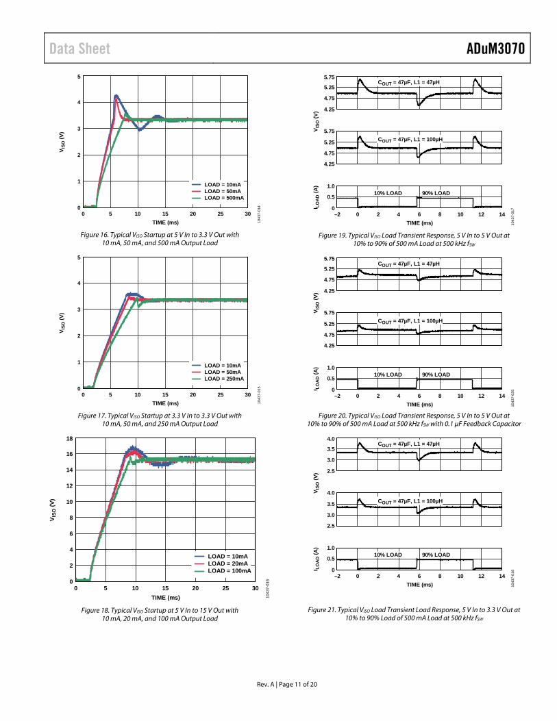
Figure 15. Typical VISO Startup at 5 V In to 5 V Out with
10 mA, 50 mA, and 500 mA Output Load
80
70
60
50
40
30
20
10
00 30025020015010050
EFFI
CIE
NC
Y (%
)
LOAD CURRENT (mA) 1043
7-03
4
TA = –40°CTA = +25°CTA = +105°C
90
80
70
60
50
40
30
20
10
00 140
EFFI
CIE
NC
Y (%
)
LOAD CURRENT (mA) 1043
7-00
9
10 20 30 40 50 60 70 80 90 100 110 120 130
fSW = 1MHzfSW = 700kHzfSW = 500kHzfSW = 200kHz
90
80
70
60
50
40
30
20
10
00 140
EFFI
CIE
NC
Y (%
)
LOAD CURRENT (mA) 1043
7-01
0
10 20 30 40 50 60 70 80 90 100 110 120 130
fSW = 1MHzfSW = 700kHzfSW = 500kHzfSW = 200kHz
90
80
70
60
50
40
30
20
10
00 140
EFFI
CIE
NC
Y (%
)
LOAD CURRENT (mA) 1043
7-01
1
10 20 30 40 50 60 70 80 90 100 110 120 130
TA = –40°CTA = +25°CTA = +105°C
80
00 70
EFFI
CIE
NC
Y (%
)
LOAD CURRENT (mA) 1043
7-01
2
10
20
30
40
50
60
70
5 10 15 20 25 30 35 40 45 50 55 60 65
5V IN TO 12V OUT5V IN TO 15V OUT
6
5
4
3
2
1
00 5 10 15 20 25 30
V ISO
(V)
TIME (ms) 1043
7-01
3
LOAD = 10mALOAD = 50mALOAD = 500mA
Rev. A | Page 10 of 20
Data Sheet ADuM3070
Figure 16. Typical VISO Startup at 5 V In to 3.3 V Out with
10 mA, 50 mA, and 500 mA Output Load
Figure 17. Typical VISO Startup at 3.3 V In to 3.3 V Out with
10 mA, 50 mA, and 250 mA Output Load
Figure 18. Typical VISO Startup at 5 V In to 15 V Out with
10 mA, 20 mA, and 100 mA Output Load
Figure 19. Typical VISO Load Transient Response, 5 V In to 5 V Out at 10% to 90% of 500 mA Load at 500 kHz fSW
Figure 20. Typical VISO Load Transient Response, 5 V In to 5 V Out at
10% to 90% of 500 mA Load at 500 kHz fSW with 0.1 µF Feedback Capacitor
Figure 21. Typical VISO Load Transient Load Response, 5 V In to 3.3 V Out at 10% to 90% Load of 500 mA Load at 500 kHz fSW
5
4
3
2
1
00 5 10 15 20 25 30
V ISO
(V)
TIME (ms) 1043
7-01
4
LOAD = 10mALOAD = 50mALOAD = 500mA
5
4
3
2
1
00 5 10 15 20 25 30
V ISO
(V)
TIME (ms) 1043
7-01
5
LOAD = 10mALOAD = 50mALOAD = 250mA
18
00 5 10 15 20 25 30
V ISO
(V)
TIME (ms) 1043
7-01
6
LOAD = 10mALOAD = 20mALOAD = 100mA
2
4
6
8
10
12
14
16
5.75
5.25
4.75
4.25
4.25
1.0
0.5
5.75
5.25
4.75
0–2 0 2 4 6 8 10 12 14
V ISO
(V)
I LO
AD
(A)
TIME (ms) 1043
7-01
7
90% LOAD10% LOAD
COUT = 47µF, L1 = 100µH
COUT = 47µF, L1 = 47µH
5.75
5.25
4.75
4.25
4.25
1.0
0.5
5.75
5.25
4.75
0–2 0 2 4 6 8 10 12 14
V ISO
(V)
I LO
AD
(A)
TIME (ms) 1043
7-03
5
90% LOAD10% LOAD
COUT = 47µF, L1 = 100µH
COUT = 47µF, L1 = 47µH
4.0
3.5
3.0
2.5
2.5
1.0
0.5
4.0
3.5
3.0
0–2 0 2 4 6 8 10 12 14
V ISO
(V)
I LO
AD
(A)
TIME (ms) 1043
7-01
8
90% LOAD10% LOAD
COUT = 47µF, L1 = 100µH
COUT = 47µF, L1 = 47µH
Rev. A | Page 11 of 20

ADuM3070 Data Sheet
Figure 22. Typical VISO Load Transient Load Response, 5 V In to 3.3 V Out at
10% to 90% Load of 500 mA Load at 500 kHz fSW with 0.1 µF Feedback Capacitor
Figure 23. Typical VISO Load Transient Response, 3.3 V In to 3.3 V Out at
10% to 90% of 250 mA Load at 500 kHz fSW
Figure 24. Typical VISO Load Transient Response, 3.3 V In to 3.3 V Out at
10% to 90% of 250 mA Load at 500 kHz fSW with 0.1 µF Feedback Capacitor
Figure 25. Typical VISO Load Transient Response, 5 V In to 15 V Out at
10% to 90% of 100 mA Load at 500 kHz fSW
Figure 26. Typical VISO Load Transient Response, 5 V In to 15 V Out at
10% to 90% of 100 mA Load at 500 kHz fSW with 0.1 µF Feedback Capacitor
Figure 27. Typical VISO Output Ripple, 5 V In to 5 V Out at
500 mA Load at 500 kHz fSW
4.0
3.5
3.0
2.5
2.5
1.0
0.5
4.0
3.5
3.0
0–2 0 2 4 6 8 10 12 14
V ISO
(V)
I LO
AD
(A)
TIME (ms) 1043
7-03
6
90% LOAD10% LOAD
COUT = 47µF, L1 = 100µH
COUT = 47µF, L1 = 47µH
4.0
3.5
3.0
2.5
2.5
1.0
0.5
4.0
3.5
3.0
0–2 0 2 4 6 8 10 12 14
V ISO
(V)
I LO
AD
(A)
TIME (ms) 1043
7-01
9
90% LOAD10% LOAD
COUT = 47µF, L1 = 100µH
COUT = 47µF, L1 = 47µH
4.0
3.5
3.0
2.5
2.5
1.0
0.5
4.0
3.5
3.0
0–2 0 2 4 6 8 10 12 14
V ISO
(V)
I LO
AD
(A)
TIME (ms) 1043
7-03
7
90% LOAD10% LOAD
COUT = 47µF, L1 = 100µH
COUT = 47µF, L1 = 47µH
18
16
14
12
12
200
100
18
16
14
0–2 0 2 4 6 8 10 12 14
V ISO
(V)
I LO
AD
(A)
TIME (ms) 1043
7-02
0
90% LOAD10% LOAD
COUT = 47µF, L1 = 100µH
COUT = 47µF, L1 = 47µH
18
16
14
12
12
200
100
18
16
14
0–2 0 2 4 6 8 10 12 14
V ISO
(V)
I LO
AD
(A)
TIME (ms) 1043
7-03
8
90% LOAD10% LOAD
COUT = 47µF, L1 = 100µH
COUT = 47µF, L1 = 47µH
1043
7-02
1
20
10
0–2
V ISO
(V)
X1 (V
)
TIME (µs)
4.94
4.98
5.02
5.06
–1 0 1 2
Rev. A | Page 12 of 20
Data Sheet ADuM3070
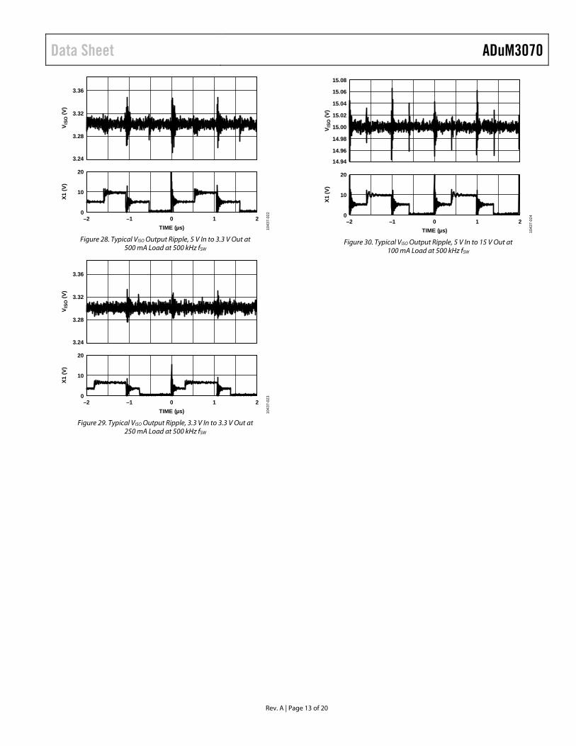
Figure 28. Typical VISO Output Ripple, 5 V In to 3.3 V Out at
500 mA Load at 500 kHz fSW
Figure 29. Typical VISO Output Ripple, 3.3 V In to 3.3 V Out at
250 mA Load at 500 kHz fSW
Figure 30. Typical VISO Output Ripple, 5 V In to 15 V Out at
100 mA Load at 500 kHz fSW
1043
7-02
2
20
10
0–2
V ISO
(V)
X1 (V
)
TIME (µs)
3.24
3.28
3.32
3.36
–1 0 1 2
1043
7-02
3
20
10
0–2
V ISO
(V)
X1 (V
)
TIME (µs)
3.24
3.28
3.32
3.36
–1 0 1 2
1043
7-02
4
20
10
0–2
V ISO
(V)
X1 (V
)
TIME (µs)
14.94
14.96
14.98
15.00
15.02
15.04
15.06
15.08
–1 0 1 2
Rev. A | Page 13 of 20
ADuM3070 Data Sheet
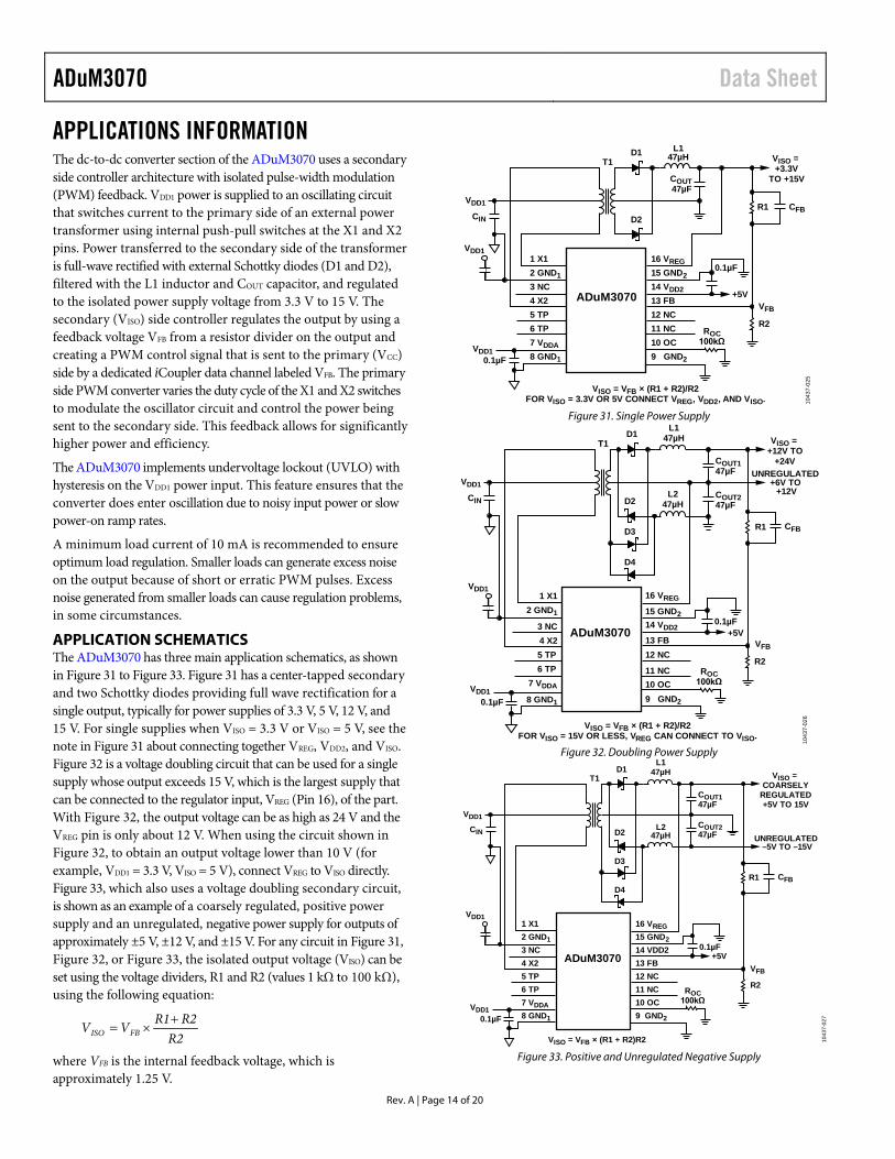
APPLICATIONS INFORMATION The dc-to-dc converter section of the ADuM3070 uses a secondary side controller architecture with isolated pulse-width modulation (PWM) feedback. VDD1 power is supplied to an oscillating circuit that switches current to the primary side of an external power transformer using internal push-pull switches at the X1 and X2 pins. Power transferred to the secondary side of the transformer is full-wave rectified with external Schottky diodes (D1 and D2), filtered with the L1 inductor and COUT capacitor, and regulated to the isolated power supply voltage from 3.3 V to 15 V. The secondary (VISO) side controller regulates the output by using a feedback voltage VFB from a resistor divider on the output and
creating a PWM control signal that is sent to the primary (VCC) side by a dedicated iCoupler data channel labeled VFB. The primary side PWM converter varies the duty cycle of the X1 and X2 switches to modulate the oscillator circuit and control the power being sent to the secondary side. This feedback allows for significantly higher power and efficiency.
The ADuM3070 implements undervoltage lockout (UVLO) with hysteresis on the VDD1 power input. This feature ensures that the converter does enter oscillation due to noisy input power or slow power-on ramp rates.
A minimum load current of 10 mA is recommended to ensure optimum load regulation. Smaller loads can generate excess noise on the output because of short or erratic PWM pulses. Excess noise generated from smaller loads can cause regulation problems, in some circumstances.
APPLICATION SCHEMATICS The ADuM3070 has three main application schematics, as shown in Figure 31 to Figure 33. Figure 31 has a center-tapped secondary and two Schottky diodes providing full wave rectification for a single output, typically for power supplies of 3.3 V, 5 V, 12 V, and 15 V. For single supplies when VISO = 3.3 V or VISO = 5 V, see the note in Figure 31 about connecting together VREG, VDD2, and VISO. Figure 32 is a voltage doubling circuit that can be used for a single supply whose output exceeds 15 V, which is the largest supply that can be connected to the regulator input, VREG (Pin 16), of the part. With Figure 32, the output voltage can be as high as 24 V and the VREG pin is only about 12 V. When using the circuit shown in Figure 32, to obtain an output voltage lower than 10 V (for example, VDD1 = 3.3 V, VISO = 5 V), connect VREG to VISO directly. Figure 33, which also uses a voltage doubling secondary circuit, is shown as an example of a coarsely regulated, positive power supply and an unregulated, negative power supply for outputs of approximately ±5 V, ±12 V, and ±15 V. For any circuit in Figure 31, Figure 32, or Figure 33, the isolated output voltage (VISO) can be set using the voltage dividers, R1 and R2 (values 1 kΩ to 100 kΩ), using the following equation:
R2R2R1VV FBISO
+×=
where VFB is the internal feedback voltage, which is approximately 1.25 V.
Figure 31. Single Power Supply
Figure 32. Doubling Power Supply
Figure 33. Positive and Unregulated Negative Supply
1043
7-02
5
ADuM3070
1 X12 GND13 NC4 X25 TP6 TP7 VDDA8 GND1
16 VREG15 GND214 VDD213 FB12 NC11 NC10 OC9 GND2
D1T1
L147µH
COUT47µF
D2
VDD1
VDD1
VDD10.1µF
CIN
0.1µF
+5V
R1
R2ROC
100kΩ
VFB
CFB
VISO = VFB × (R1 + R2)/R2FOR VISO = 3.3V OR 5V CONNECT VREG, VDD2, AND VISO.
VISO =+3.3V
TO +15V
1043
7-02
6
ADuM3070
D1T1
L147µH
L247µH
COUT147µF
COUT247µFD2
D3
D4
VDD1
VDD10.1µF
CIN
0.1µF+5V
R1
R2
VFB
ROC100kΩ
VISO = VFB × (R1 + R2)/R2FOR VISO = 15V OR LESS, VREG CAN CONNECT TO VISO.
VISO =+12V TO
+24VUNREGULATED
+6V TO+12V
VDD11 X1
2 GND1
3 NC4 X25 TP6 TP
7 VDDA
8 GND1
16 VREG
15 GND214 VDD2
13 FB12 NC
11 NC10 OC9 GND2
CFB
1043
7-02
7
ADuM3070
1 X12 GND13 NC4 X25 TP6 TP7 VDDA8 GND1
16 VREG15 GND214 VDD213 FB12 NC11 NC10 OC9 GND2
D1T1
L147µH
L247µH
COUT147µF
COUT247µFD2
D3
D4
VDD1
VDD10.1µF
CIN
0.1µF+5V
R1
R2ROC100kΩ
VFB
VISO = VFB × (R1 + R2)R2
VISO =COARSELY
REGULATED+5V TO 15V
UNREGULATED–5V TO –15V
VDD1
CFB
Rev. A | Page 14 of 20
Data Sheet ADuM3070
TRANSFORMER DESIGN Transformers have been designed for use in the circuits shown in Figure 31, Figure 32, and Figure 33 and are listed in Table 13. The design of a transformer for the ADuM3070 can differ from some isolated dc-to-dc converter designs that do not regulate the output voltage. The output voltage is regulated by a PWM controller in the ADuM3070 that varies the duty cycle of the primary side switches in response to a secondary side feedback voltage, VFB, received through an isolated digital channel. The internal controller has a limit of 40% maximum duty cycle.
TRANSFORMER TURNS RATIO To determine the transformer turns ratio, and taking into account the losses for the primary switches and the losses for the secondary diodes and inductors, the external transformer turns ratio for the ADuM3070 can be calculated by
2××+
=DV
VVNN
(MIN)DD1
DISO
P
S
where: NS/NP is the primary to secondary turns ratio. VISO is the isolated output supply voltage. VD is the Schottky diode voltage drop (0.5 V maximum). VDD1 (MIN) is the minimum input supply voltage. D is the duty cycle = 0.30 for a 30% typical duty cycle, 40% is maximum, and a multiplier factor of 2 is used for the push-pull switching cycle.
For Figure 31, the 5 V to 5 V reference design in Table 13, with VDD1 (MIN) = 4.5 V, the turns ratio is NS/NP = 2.
For a similar 3.3 V input to 3.3 V output, isolated single power supply and with VDD1 (MIN) = 3.0 V, the turns ratio is also NS/NP = 2. Therefore, the same transformer turns ratio NS/NP = 2 can be used for the three single power applications (5 V to 5 V, 5 V to 3.3 V, and 3.3 V to 3.3 V).
For Figure 32, the circuit uses double windings and diode pairs to create a doubler circuit; therefore, half the output voltage, VISO/2, is used in the equation.
22
××
+=
DV
VV
NN
(MIN)DD1
DISO
P
S
NS/NP is the primary to secondary turns ratio. VISO/2 is used in the equation because the circuit uses two pairs of diodes creating a doubler circuit. VD is the Schottky diode voltage drop (0.5 V maximum). VDD1 (MIN) is the minimum input supply voltage. D is the duty cycle, which is 0.30 for a 30% typical duty cycle and 0.40 for a 40% maximum duty cycle, and a multiplier factor of two is used for the push-pull switching cycle.
For Figure 32, the 5 V to 15 V reference design in Table 13, with VDD1 (MIN) = 4.5 V, results in a turns ratio of NS/NP = 3.
For Figure 33, the circuit also uses double windings and diode pairs to create a doubler circuit; however, because a positive and negative output voltage is created, VISO is used in the equation.
2××+
=DV
VVNN
(MIN)DD1
DISO
P
S
where: NS/NP is the primary to secondary turns ratio. VISO is the isolated output supply voltage and is used in the equation because the circuit uses two pairs of diodes creating a doubler circuit with a positive and negative output. VD is the Schottky diode voltage drop (0.5 V maximum). VDD1 (MIN) is the minimum input supply voltage, and a multiplier factor of 2 is used for the push-pull switching cycle. D is the duty cycle; in this case, a higher duty cycle of D = 0.35 for a 35% typical duty cycle (40% maximum duty cycle) was used in the Figure 33 circuit to reduce the maximum voltages seen by the diodes for a ±15 V supply.
For Figure 33, the +5 V to ±15 V reference design in Table 13, with VDD1 (MIN) = 4.5 V, results in a turns ratio of NS/NP = 5.
TRANSFORMER ET CONSTANT The next transformer design factor to consider is the ET constant. This constant determines the minimum V × µs constant of the transformer over the operating temperature. ET values of 14 V × µs and 18 V × µs were selected for the ADuM3070 designs listed in Table 13 using the following equation:
2)(
)( ×=
MINSW
(MAX)DD1
f
VMINET
where: VDD1 (MAX) is the maximum input supply voltage. fSW (MIN) is the minimum primary switching frequency = 300 kHz in startup, and a multiplier factor of 2 is used for the push-pull switching cycle.
TRANSFORMER PRIMARY INDUCTANCE AND RESISTANCE Another important characteristic of the transformer for designs with the ADuM3070 is the primary inductance. Transformers for the ADuM3070 are recommended to have between 60 µH to 100 µH of inductance per primary winding. Values of primary inductance in this range are needed for smooth operation of the ADuM3070 pulse-by-pulse current-limit circuit, which can help protect against build up of saturation currents in the transformer. If the inductance is specified for the total of both primary windings, for example, as 400 µH, the inductance of one winding is ¼ of two equal windings, or 100 µH.
Another important characteristic of the transformer for designs with the ADuM3070 is primary resistance. Primary resistance as low as is practical (less than 1 Ω) helps reduce losses and improves efficiency. The total primary resistance can be measured and specified, and is shown for the transformers in Table 13.
Rev. A | Page 15 of 20

ADuM3070 Data Sheet Table 13. Transformer Reference Designs
Part No. Manufacturer Turns Ratio, PRI:SEC
ET Constant (V × µs Min)
Total Primary Inductance (µH)
Total Primary Resistance (Ω)
Isolation Voltage (rms)
Isolation Type Reference
JA4631-BL Coilcraft 1CT:2CT 18 255 0.2 2500 Basic Figure 31 JA4650-BL Coilcraft 1CT:3CT 18 255 0.2 2500 Basic Figure 32 KA4976-AL Coilcraft 1CT:5CT 18 255 0.2 2500 Basic Figure 33
TGSAD-260V6LF Halo Electronics 1CT:2CT 14 389 0.8 2500 Supplemental Figure 31 TGSAD-290V6LF Halo Electronics 1CT:3CT 14 389 0.8 2500 Supplemental Figure 32 TGSAD-292V6LF Halo Electronics 1CT:5CT 14 389 0.8 2500 Supplemental Figure 33
TGAD-260NARL Halo Electronics 1CT:2CT 14 389 0.8 1500 Functional Figure 31 TGAD-290NARL Halo Electronics 1CT:3CT 14 389 0.8 1500 Functional Figure 32 TGAD-292NARL Halo Electronics 1CT:5CT 14 389 0.8 1500 Functional Figure 33
TRANSFORMER ISOLATION VOLTAGE Isolation voltage and isolation type should be determined for the requirements of the application and then specified. The transformers in Table 13 have been specified for 2500 V rms for supplemental or basic isolation and for 1500 V rms for functional isolation. Other isolation levels and isolation voltages can be specified and requested from the manufacturers that are listed in Table 13 or from other manufacturers.
SWITCHING FREQUENCY The ADuM3070 switching frequency can be adjusted from 200 kHz to 1 MHz by changing the value of the ROC resistor shown in Figure 31, Figure 32, and Figure 33. The value of the ROC resistor needed for the desired switching frequency can be determined from the switching frequency vs. ROC resistance curve shown in Figure 4. The output filter inductor value and output capacitor value for the ADuM3070 application schematics have been designed to be stable over the switching frequency range from 500 kHz to 1 MHz, when loaded from 10% to 90% of the maximum load.
The ADuM3070 also has an open-loop mode where the output voltage is not regulated and is dependent on the transformer turns ratio, NS/NP, and the conditions of the output including output load current and the losses in the dc-to-dc converter circuit. This open-loop mode is selected when the OC pin is connected high to the VDD2 pin. In open-loop mode, the switching frequency is 318 kHz.
TRANSIENT RESPONSE The load transient response of the output voltage of the ADuM3070 for 10% to 90% of the full load is shown in Figure 19 to Figure 26 for the application schematics in Figure 31 and Figure 32. The response shown is slow but stable and can have more output change than desired for some applications. The output voltage change with load transient has been reduced, and the output has been shown to remain stable by adding more inductance to the output circuits, as shown in the second VISO output waveform in Figure 19 to Figure 26.
For additional improvement in transient response, add a 0.1 µF ceramic capacitor (CFB) in parallel with the high feedback resistor. As shown in Figure 19 to Figure 26, this value helps reduce the overshoot and undershoot during load transients.
COMPONENT SELECTION Power supply bypassing is required at the input and output supply pins. Note that a low ESR ceramic bypass capacitor of 0.1 µF is required on Side 1 between Pin 7 and Pin 8, and on Side 2 between Pin 14 and Pin 15, as close to the chip pads as possible.
The power supply section of the ADuM3070 uses a high oscillator frequency to efficiently pass power through the external power transformer. Bypass capacitors are required for several operating frequencies. Noise suppression requires a low inductance, high frequency capacitor; ripple suppression and proper regulation require a large value capacitor. To suppress noise and reduce ripple, large valued ceramic capacitors of X5R or X7R dielectric type are recommended. The recommended capacitor value is 10 µF for VDD1 and 47 µF for VISO. These capacitors have a low ESR and are available in moderate 1206 or 1210 sizes for voltages up to 10 V. For output voltages larger than 10 V, two 22 µF ceramic capacitors can be used in parallel. See Table 14 for recommended components.
Inductors must be selected based on the value and supply current needed. Most applications with switching frequencies between 500 kHz and 1 MHz and load transients between 10% and 90% of full load are stable with the 47 µH inductor value listed in Table 14. Values as large as 200 µH can be used for power supply applications with a switching frequency as low as 200 kHz to help stabilize the output voltage or for improved load transient response (see Figure 19 to Figure 26). Inductors in a small 1212 or 1210 size are listed in Table 14 with a 47 µH value and a 0.41 A current rating to handle the majority of applications below a 400 mA load, and with a 100 µH value and a 0.34 A current rating to handle a load to 300 mA.
Schottky diodes are recommended for their low forward voltage to reduce losses and their high reverse voltage of up to 40 V to withstand the peak voltages available in the doubling circuit shown in Figure 32 and Figure 33.
Rev. A | Page 16 of 20
Data Sheet ADuM3070
Rev. A | Page 17 of 20
Table 14. Recommended Components Part Number Manufacturer Value GRM32ER71A476KE15L Murata 47 μF, 10 V, X7R,
1210 GRM32ER71C226KEA8L Murata 22 μF, 16 V, X7R,
1210 GRM31CR71A106KA01L Murata 10 μF, 10 V, X7R,
1206 MBR0540T1/D ON Semiconductor 0.5 A, 40 V,
Schottky, SOD-123 LQH3NPN470MM0 Murata 47 μH, 0.41 A,
1212 ME3220-104KL Coilcraft 100 μH, 0.34 A,
1210
PRINTED CIRCUIT BOARD (PCB) LAYOUT Note that the total lead length between the ends of the low ESR capacitor and the VDDx and GNDx pins must not exceed 2 mm. See Figure 34 for the recommended PCB layout.
Figure 34. Recommended PCB Layout
In applications involving high common-mode transients, ensure that board coupling across the isolation barrier is minimized. Furthermore, design the board layout such that any coupling that does occur equally affects all pins on a given component side. Failure to ensure this can cause voltage differentials between pins, exceeding the absolute maximum ratings specified in Table 10, thereby leading to latch-up and/or permanent damage.
The ADuM3070 is a power device that dissipates about 1 W of power when fully loaded. Because it is not possible to apply a heat sink to an isolation device, the device primarily depends on heat dissipation into the PCB through the GNDx pins. If the device is used at high ambient temperatures, care must be taken to provide a thermal path from the GNDx pins to the PCB ground plane.
The board layout shows enlarged pads for the GNDx pins (Pin 2 and Pin 8) on Side 1 and (Pin 9 and Pin 15) on Side 2. Implement large diameter vias from the pad to the ground planes and power planes to increase thermal conductivity and to reduce inductance. Multiple vias in the thermal pads can significantly reduce temperatures inside the chip. The dimensions of the expanded pads are left to the discretion of the designer and the available board space.
THERMAL ANALYSIS The ADuM3070 parts consist of two internal die attached to a split lead frame with two die attach paddles. For the purposes of thermal analysis, the die is treated as a thermal unit, with the highest junction temperature reflected in the θJA from Table 5. The value of θJA is based on measurements taken with the devices mounted on a JEDEC standard, 4-layer board with fine width traces and still air. Under normal operating conditions, the ADuM3070 devices operate at full load across the full temperature range without derating the output current. However, following the recommendations in the Printed Circuit Board (PCB) Layout section decreases thermal resistance to the PCB, allowing increased thermal margins in high ambient temperatures. The ADuM3070 has a thermal shutdown circuit that shuts down the dc-to-dc converter of the ADuM3070 when a die temperature of about 160°C is reached. When the die cools below about 140°C, the ADuM3070 dc-to-dc converter turns on again.
POWER CONSUMPTION The total input supply current is equal to the sum of the IDD1 primary transformer current and the ADuM3070 input current, IDDA.
The following relationship allows the total IIN current to be:
IIN = (IISO × VISO)/(E × VDD1) (1)
where: IIN is the total supply input current. IISO is the current drawn by the secondary side external load. E is the power supply efficiency at the given output load from Figure 8 or Figure 14 at the VISO and VDD1 condition of interest.
Figure 35. Supply Currents
X1
X2NC
TPTP
NCNC
GND1
GND1
VREG
GND2VDD2
FB
VDDA OCGND2
1043
7-02
8
ADuM3070
1043
7-02
9
PRIMARYCONVERTER/
DRIVER SECONDARYCONTROLLER
INTERNALFEEDBACK
VDD2
OC
FB
VREG
VDD1 IDD1IIN VISO IISO
VDDAIDDA
X2X1
GND1 GND2
REG
RECT
5V
NOTES1. VDD1 IS THE POWER SUPPLY FOR THE PUSH-PULL TRANSFORMER.2. VDDA IS THE POWER SUPPLY OF SIDE 1 OF THE ADuM3070.

ADuM3070 Data Sheet
POWER CONSIDERATIONS Soft Start Mode and Current-Limit Protection
When the ADuM3070 first receives power from VDD1, it is in soft start mode, and the output voltage, VISO, is increased gradually while it is below the startup threshold. In soft start mode, to limit the peak current during VISO power-up, the primary converter gradually increases the width of the PWM signal. When the output voltage is larger than the start-up threshold, the PWM signal can be transferred from the secondary controller to the primary converter, and the dc-to-dc converter switches from soft start mode to the normal PWM control mode. If a short circuit occurs, the push-pull converter shuts down for about 2 ms and then enters soft start mode. If, at the end of soft start, a short circuit still exists, the process is repeated, which is called hiccup mode. If the short circuit is cleared, the ADuM3070 enters normal operation.
The ADuM3070 has a pulse-by-pulse current limit, which is active at startup and during normal operation, that protects the primary switches, X1 and X2, from exceeding approximately 1.3 A peak, protecting the transformer windings.
INSULATION LIFETIME All insulation structures eventually break down when subjected to voltage stress over a sufficiently long period. The rate of insulation degradation is dependent on the characteristics of the voltage waveform applied across the insulation. Analog Devices, Inc., conducts an extensive set of evaluations to determine the lifetime of the insulation structure within the ADuM3070. Accelerated life testing is performed using voltage levels higher than the rated continuous working voltage. Acceleration factors for several operating conditions are determined, allowing calculation of the time to failure at the working voltage of interest. The values shown in Table 11 summarize the peak voltages for 50 years of service life in several operating conditions. In many cases, the working voltage approved by agency testing is higher than the 50-year service life voltage. Operation at working voltages higher than the service life voltage listed leads to premature insulation failure.
The insulation lifetime of the ADuM3070 depends on the voltage waveform type imposed across the isolation barrier. The iCoupler insulation structure degrades at different rates, depending on whether the waveform is bipolar ac, dc, or unipolar ac. Figure 36, Figure 37, and Figure 38 illustrate these different isolation voltage waveforms.
Bipolar ac voltage is the most stringent environment. A 50-year operating lifetime under the bipolar ac condition determines the Analog Devices recommended maximum working voltage.
In the case of unipolar ac or dc voltage, the stress on the insulation is significantly lower. This allows operation at higher working voltages while still achieving a 50-year service life. The working voltages listed in Table 11 can be applied while maintaining the 50-year minimum lifetime, if the voltage conforms to either the unipolar ac or dc voltage cases. Treat any cross-insulation voltage waveform that does not conform to Figure 37 or Figure 38 as a bipolar ac waveform, and limit its peak voltage to the 50-year lifetime voltage value listed in Table 11.
Figure 36. Bipolar AC Waveform
Figure 37. DC Waveform
Figure 38. Unipolar AC Waveform
0V
RATED PEAK VOLTAGE
1043
7-03
0
0V
RATED PEAK VOLTAGE
1043
7-03
1
0V
RATED PEAK VOLTAGE
1043
7-03
2
NOTES1. THE VOLTAGE IS SHOWN SINUSOIDAL
FOR ILLUSTRATION PURPOSES ONLY.IT IS MEANT TO REPRESENT ANY VOLTAGEWAVEFORM VARYING BETWEEN 0 AND SOMELIMITING VALUE. THE LIMITING VALUE CAN BEPOSITIVE OR NEGATIVE, BUT THE VOLTAGECANNOT CROSS 0V.
Rev. A | Page 18 of 20
Data Sheet ADuM3070
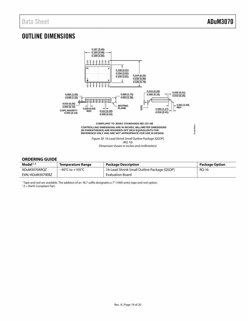
OUTLINE DIMENSIONS
Figure 39. 16-Lead Shrink Small Outline Package [QSOP]
(RQ-16) Dimension shown in inches and (millimeters)
ORDERING GUIDE Model1, 2 Temperature Range Package Description Package Option ADuM3070ARQZ −40°C to +105°C 16-Lead Shrink Small Outline Package [QSOP] RQ-16 EVAL-ADuM3070EBZ Evaluation Board
1 Tape and reel are available. The addition of an -RL7 suffix designates a 7” (1000 units) tape and reel option. 2 Z = RoHS Compliant Part.
COMPLIANT TO JEDEC STANDARDS MO-137-ABCONTROLLING DIMENSIONS ARE IN INCHES; MILLIMETER DIMENSIONS(IN PARENTHESES) ARE ROUNDED-OFF INCH EQUIVALENTS FORREFERENCE ONLY AND ARE NOT APPROPRIATE FOR USE IN DESIGN.
16 9
81
SEATINGPLANE
0.010 (0.25)0.004 (0.10)
0.012 (0.30)0.008 (0.20)
0.025 (0.64)BSC
0.041 (1.04)REF
0.010 (0.25)0.006 (0.15)
0.050 (1.27)0.016 (0.41)
0.020 (0.51)0.010 (0.25)
8°0°COPLANARITY
0.004 (0.10)
0.065 (1.65)0.049 (1.25)
0.069 (1.75)0.053 (1.35)
0.197 (5.00)0.193 (4.90)0.189 (4.80)
0.158 (4.01)0.154 (3.91)0.150 (3.81) 0.244 (6.20)
0.236 (5.99)0.228 (5.79)
01-2
8-20
08-A
Rev. A | Page 19 of 20

ADuM3070 Data Sheet
NOTES
©2012–2014 Analog Devices, Inc. All rights reserved. Trademarks and registered trademarks are the property of their respective owners. D10437-0-5/14(A)
Rev. A | Page 20 of 20