isscc 2014 / session 23 / energy harvesting /...
TRANSCRIPT
396 • 2014 IEEE International Solid-State Circuits Conference
ISSCC 2014 / SESSION 23 / ENERGY HARVESTING / 23.2
23.2 A 1.1nW Energy Harvesting System with 544pW Quiescent Power for Next-Generation Implants
Saurav Bandyopadhyay1,*, Patrick P. Mercier1,2, Andrew C. Lysaght3, Konstantina M. Stankovic3,4, Anantha P. Chandrakasan1
1Massachusetts Institute of Technology, Cambridge, MA, 2University of California, San Diego, La Jolla, CA, 3Massachusetts Eye and Ear Infirmary, Boston, MA, 4Massachusetts General Hospital, Harvard Medical School, Boston, MA, *Now at Texas Instruments, Dallas, TX,
A wireless sensor that is powered from the endocochlear potential (EP), a 70-to-100mV bio-potential inside the mammalian ear, has been demonstrated in [1].Due to the anatomical size and physiological constraints inside the ear, a maximum of 1.1 to 6.25nW can be extracted from the EP. The nanowatt powerbudget of the sensor gives rise to unique challenges with power conversion efficiency and quiescent current reduction in the power management unit(PMU). While [1] presents the system aspects of the biomedical harvestingincluding the biologic interface and system measurements, this work presentsthe details of the nanowatt PMU required to power the electronics. More specifically, it focuses on the low-power circuit design techniques needed torealize a nW power converter that is applicable to a broad spectrum of emergingbiomedical applications with ultra-low energy-harvesting sources.
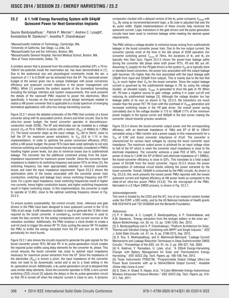
Figure 23.2.1 shows the detailed schematic of the PMU that consists of a boostconverter along with its associated control, drivers and timer circuits. Due to theultra-low power budget, the boost converter operates in discontinuous- conduction mode (DCM). The EP and electrodes can be modeled as a voltagesource (VEP of 70 to 100mV) in series with a resistor (Relec) of 400kΩ to 1.2MΩ[1]. The boost converter steps up the input voltage, VIN (30 to 55mV, close tohalf the EP for maximum power extraction), to VDD (0.8 to 1.1V in this implementation). In order to optimize the power conversion efficiency (PCE)within a nW power budget, the power FETs have been sized optimally to not onlyminimize switching and conduction losses that are normally considered in PMUshandling higher power levels, but also to minimize losses due to subthresholdleakage. The converter has the additional constraint arising from the input-impedance requirement for maximum power transfer. Since the converter inputimpedance is related to its switching frequency and power FETs on times [2], theswitching frequency has been appropriately selected to minimize converter losses and meet the input impedance requirement. Figure 23.2.2 shows the optimization plots of the losses associated with the converter power train (conduction, switching and leakage loss) versus switching frequency and FETsizes. For a given input impedance, lower switching frequencies result in higherrms currents, hence higher conduction losses, and higher switching frequenciesresult in higher switching losses. In this implementation, the converter is madeto operate at 12.8Hz, close to the optimal switching frequency shown in Fig.23.2.2.
To ensure system sustainability, the control circuits, timer, reference and gatedrivers in the PMU have been designed to have quiescent current in the 10 to100s of pA range. A pW relaxation oscillator is used to generate the 12.8Hz clockrequired by the boost converter. A constant-gm current reference in used to create the bias currents for the analog comparators and current sources in therelaxation oscillator. Additionally, the PMU employs a clock divider to create asub-Hz clock to trigger the sensor RF TX. Duty cycling the sensor RF-TX enablesthe PMU to buffer the energy extracted from the EP and turn on the RF-TX periodically for short bursts.
Figure 23.2.1 also shows the circuits required to generate the gate signals for theboost converter power FETs N0 and P0. A Φ1-pulse-generation circuit createsthe required pulse widths using delay elements for the converter Φ1 phase. Thiscircuit ensures the boost converter has close to optimal input impedance necessary for maximum power extraction from the EP. Since the impedance ofthe electrodes (Relec) is known a priori, the input impedance of the converterdoes not need to be dynamically varied and is set to a fixed setting in the Φ1-generation circuit. Additionally, a Φ2-pulse-generation circuit is designed thatuses similar delay elements. Since the converter operates in DCM, a zero currentswitching (ZCS) circuit [2] adjusts the delays in the Φ2-pulse-generation circuitso that P0 is turned off when the inductor current is close to zero. A dynamic
comparator clocked with a delayed version of the Φ2 pulse compares VDRAIN withVDD. By using an increment/decrement logic, a 3b code is adjusted that sets theΦ2 pulse width. Digital implementations of these circuits help minimize the quiescent current. Logic transistors in the gate drivers and the pulse generationcircuits have been sized to minimize leakage while meeting the desired speedrequirements.
The PMU utilizes a voltage doubler to minimize losses arising from subthresholdleakage in the boost converter power train. Due to the low output current, theconverter spends most of the time in the idle phase of DCM operation (for converter switching period Tperiod of 78ms, the durations of Φ1 and Φ2 are typically less than 5μs). Figure 23.2.3 shows the power-train leakage paths during the converter idle phase when both power FETs, P0 and N0, are off.Assuming VX (supply for the P0 gate driver) is the system VDD as is typically donein standard boost converters, the power loss associated with the output leakagepath becomes 10× higher than the loss associated with the input leakage path(20pW from input and 223pW from output). This is mainly due to the fact thatVDD is much higher than VIN for the boost converter. Since the output leakagecurrent is governed by the subthreshold leakage in P0, by using the voltage doubler, an elevated supply, VPUMP, is generated to drive the gate of P0. Whenoff, P0 sees a negative source to gate voltage, putting it in super cut-off andreducing its subthreshold leakage [3]. Although the voltage doubler too has leakage paths of its own as shown in Fig. 23.2.3, the transistors are much smaller than the power FET P0. Even with the overhead of VPUMP generation andincreased switching losses in the P0 gate driver, the overall power saving (simulated) due to the voltage doubler is 175 to 188pW (17% of the minimumpower budget) in the typical corner and 950pW in the fast corner making theconverter robust towards process variations.
Figure 23.2.4 shows the boost-converter output power and the correspondingefficiency with an electrode impedance of 1MΩ and EP of 80 to 100mV (emulated using a 1MΩ resistor and a power supply in this measurement) for aVDD of 0.9V and boost converter inductance of 47μH. The converter is characterized for various input voltages by varying the boost converter inputimpedance. The maximum output power is achieved for an input voltage closeto half of the EP which is when the converter input impedance is close to theelectrode impedance. The converter achieves a peak PCE of 56%. For inputpower of close to 1.2nW (for EP of 80mV and electrode impedance of 1.28MΩ),the boost-converter efficiency is close to 53%. This translates to a total outputpower of 637pW from the boost converter. Figure 23.2.5 shows the power consumption of individual circuit blocks utilizing the power extracted by theboost converter. Overall, 544pW is consumed by the PMU circuits. As shown inFig. 23.2.6, this work presents the lowest power PMU reported with the lowestquiescent current and highest efficiency at nW power levels as compared to thestate-of-art ultra-low power PMUs [4,5,6]. The die micrograph of the PMU, fabricated in a 0.18μm CMOS process, is shown in Fig. 23.2.7.
Acknowledgements:This work is funded by the C2S2 and the IFC, two of six research centers fundedunder the FCRP, a SRC entity, and by the US National Institutes of Health grantsK08 DC010419 and T32 DC00038 and the Bertarelli Foundation.
References:[1] P. P. Mercier, A. C. Lysaght, S. Bandyopadhyay, A. P. Chandrakasan, andK.M. Stankovic, “Energy extraction from the biologic battery in the inner ear,”Nature Biotechnology, vol. 30, no. 12, pp. 1240-1243, Dec. 2012.[2] S. Bandyopadhyay and A. P. Chandrakasan, “Platform Architecture for Solar,Thermal and Vibration Energy Combining with MPPT and Single Inductor,” IEEEJ. Solid State Circuits, vol. 47, no. 9, pp. 2199-2215, Sep. 2012.[3] K. Roy, S. Mukhopadhyay, and H. Mahmoodi-Meimand, “Leakage CurrentMechanisms and Leakage Reduction Techniques in Deep-Submicrometer CMOSCircuits,” Proceedings of the IEEE, vol. 91, no. 2, pp. 305-327, Feb. 2003.[4] K. Kadirvel, Y. Ramadass, U. Lyles, et.al., “A 330nA Energy-HarvestingCharger with Battery Management for Solar and Thermoelectric EnergyHarvesting,” IEEE ISSCC Dig. Tech. Papers, pp. 106-108, Feb. 2012.[5] Texas Instruments TPS62736, “Programmable Output Voltage Ultra-LowPower Buck Converter with up to 50mA/200mA Output Current,” AvailableOnline http://www.ti.com/ .[6] G. Chen, H. Ghaed. R. Haque, et.al., “A Cubic-Millimeter Energy-AutonomousWireless Intraocular Pressure Monitor,” IEEE ISSCC Dig. Tech. Papers, pp. 310-311, Feb. 2011.
978-1-4799-0920-9/14/$31.00 ©2014 IEEE

397DIGEST OF TECHNICAL PAPERS •
ISSCC 2014 / February 12, 2014 / 9:00 AM
Figure 23.2.1: Power management unit (PMU) for harvesting energy from theendocochlear potential (EP).
Figure 23.2.2: Loss (overall loss due to conduction, switching and leakage)optimization plots versus converter switching frequency and power FET size inDCM for a given input impedance (1.6MΩ) at input voltage of 40mV with boostconverter inductance of 47µH.
Figure 23.2.3: Boost converter leakage paths and voltage doubler currentpaths.
Figure 23.2.5: Measured power consumption of individual circuit blocks. Figure 23.2.6: Comparison with previously published low-power PMUs inenergy harvesting systems.
Figure 23.2.4: Boost converter measured results showing output power andcorresponding efficiency.
I
CEP
L
Φ2Φ1
L V DD
CDD+_
Boost Converter
Drivers, Control & Leakage Reduction Circuits
EndocochlearPotential model
12.8 Hz
Relec
To triggerTx every40-360 s
Timer and Reference V DD V PUMP
VoltageDoubler CPUMP
VDD
V PUMP
V IN
V EP
CPAR,EFF
N0
P0V DRAIN
ClockDivider
CurrentRef.
Relaxation Osc.
Set for Input Impedance
Increment/Decerment
LogicDQ
+-
Φ1
V DD
V DRAIN
Φ2
3-bit ZCS Circuit
Φ Pulse Gen.1 Φ Pulse Gen.2
5 10 15 20 25 30 35 40 45 50300
400
500
600
700
800
0.5 1 1.5 2 2.5200
400
600
800
1000
1200
1400
400
500
600
700
Switching Frequency (f )s
Loss
(pW
)
0.5 1 1.5 2 2.5Normalized WN0 Normalized WP0
Loss
(pW
)
Loss
(pW
)
Loss v/s f at W =W ,W =Ws N0 N0,opt P0,optP0
fs,opt
Loss v/s W at W =W ,f =fsP0,optP0 s,optN0
WN,opt WP,opt
Loss v/s W at W =W ,f =fsN0,optN0 s,optP0
V DDV IN
N0
P0
V X
Leakage from Input Leakage from Output
(40mV) (0.9V)
V PUMP
V DD
V DD V DDV DD
V PUMP
VPUMP
V DD
GNDV DD
I LEAK1
I LEAK2I LEAK3
I LEAK4I SW1
I SW2
Boost Converter Leakage Reduction with Voltage Doubler
Volatge Doubler Current Paths including leakage
0.2
0.4
0.6
0.8
1.0
1.2
1.4
1.6
Input Voltage (mV)
Out
put P
ower
(nW
)
10 20 30 40 50 60 70 80 90
0.42
0.44
0.46
0.48
0.5
0.52
0.54
0.56
0.58
Input Voltage (mV)E
ffici
ency
Emulated EP = 80mVEmulated EP = 100mV
10 20 30 40 50 60 70 80 90
Emulated EP = 80mVEmulated EP = 100mV
ESD circuits
Impedance AdjustmentZCS and N0 Driver
Timer and CurrentReference
Voltage Doubler andP0 Driver
Tx and other loads352.8 pW
91.8 pW
81.9 pW
93.6 pW
17.1 pW
23

• 2014 IEEE International Solid-State Circuits Conference 978-1-4799-0920-9/14/$31.00 ©2014 IEEE
ISSCC 2014 PAPER CONTINUATIONS
Figure 23.2.7: Die micrograph showing the PMU details.