itg-3400 product specification revision 1akizukidenshi.com/download/ds/invensense/ps-itg-34… ·...
TRANSCRIPT
InvenSense Inc.
1745 Technology Drive, San Jose, CA 95110 U.S.A.
Tel: +1 (408) 988-7339 Fax: +1 (408) 988-8104
Website: www.invensense.com
Document Number: PS-ITG-3400A-00 Revision: 1.0 Release Date: 12/24/2013
1 of 41
ITG-3400
Product Specification
Revision 1.0
ITG-3400 Product Specification Document Number: PS-ITG-3400A-00 Revision: 1.0 Release Date: 12/24/2013
2 of 41
TABLE OF CONTENTS
TABLE OF FIGURES ......................................................................................................................................... 4
TABLE OF TABLES .......................................................................................................................................... 5
1 DOCUMENT INFORMATION ...................................................................................................................... 6
1.1 REVISION HISTORY .............................................................................................................................. 6
1.2 PURPOSE AND SCOPE .......................................................................................................................... 7
1.3 PRODUCT OVERVIEW ........................................................................................................................... 7
1.4 APPLICATIONS ..................................................................................................................................... 7
2 FEATURES .................................................................................................................................................. 8
2.1 GYROSCOPE FEATURES ....................................................................................................................... 8
2.2 ADDITIONAL FEATURES ........................................................................................................................ 8
3 ELECTRICAL CHARACTERISTICS ........................................................................................................... 9
3.1 GYROSCOPE SPECIFICATIONS .............................................................................................................. 9
3.2 ELECTRICAL SPECIFICATIONS ............................................................................................................. 10
3.3 I2C TIMING CHARACTERIZATION ......................................................................................................... 13
3.4 SPI TIMING CHARACTERIZATION ......................................................................................................... 14
3.5 ABSOLUTE MAXIMUM RATINGS ........................................................................................................... 15
4 APPLICATIONS INFORMATION .............................................................................................................. 16
4.1 PIN OUT DIAGRAM AND SIGNAL DESCRIPTION ..................................................................................... 16
4.2 TYPICAL OPERATING CIRCUIT ............................................................................................................. 17
4.3 BILL OF MATERIALS FOR EXTERNAL COMPONENTS .............................................................................. 17
4.4 BLOCK DIAGRAM ............................................................................................................................... 18
4.5 OVERVIEW ........................................................................................................................................ 18
4.6 THREE-AXIS MEMS GYROSCOPE WITH 16-BIT ADCS AND SIGNAL CONDITIONING ................................ 18
4.7 I2C AND SPI SERIAL COMMUNICATIONS INTERFACES .......................................................................... 19
4.8 CLOCKING ......................................................................................................................................... 20
4.9 SENSOR DATA REGISTERS ................................................................................................................. 20
4.10 FIFO ................................................................................................................................................ 21
4.11 INTERRUPTS ...................................................................................................................................... 21
4.12 DIGITAL-OUTPUT TEMPERATURE SENSOR .......................................................................................... 21
4.13 BIAS AND LDOS ................................................................................................................................ 21
4.14 CHARGE PUMP .................................................................................................................................. 21
4.15 STANDARD POWER MODES ................................................................................................................ 21
5 PROGRAMMABLE INTERRUPTS ............................................................................................................ 23
ITG-3400 Product Specification Document Number: PS-ITG-3400A-00 Revision: 1.0 Release Date: 12/24/2013
3 of 41
6 DIGITAL INTERFACE ............................................................................................................................... 24
6.1 I2C AND SPI SERIAL INTERFACES ...................................................................................................... 24
6.2 I2C INTERFACE .................................................................................................................................. 24
6.3 I2C COMMUNICATIONS PROTOCOL ..................................................................................................... 24
6.4 I2C TERMS ........................................................................................................................................ 27
6.5 SPI INTERFACE ................................................................................................................................. 28
7 SERIAL INTERFACE CONSIDERATIONS ............................................................................................... 29
7.1 ITG-3400 SUPPORTED INTERFACES ................................................................................................... 29
8 ASSEMBLY ............................................................................................................................................... 30
8.1 ORIENTATION OF AXES ...................................................................................................................... 30
8.2 PACKAGE DIMENSIONS ...................................................................................................................... 31
8.3 PCB DESIGN GUIDELINES .................................................................................................................. 32
8.4 ASSEMBLY PRECAUTIONS .................................................................................................................. 33
8.5 STORAGE SPECIFICATIONS ................................................................................................................. 36
8.6 PACKAGE MARKING SPECIFICATION .................................................................................................... 36
8.7 TAPE & REEL SPECIFICATION ............................................................................................................. 37
8.8 LABEL ............................................................................................................................................... 38
8.9 PACKAGING ....................................................................................................................................... 39
8.10 REPRESENTATIVE SHIPPING CARTON LABEL ....................................................................................... 40
9 ENVIRONMENTAL COMPLIANCE ........................................................................................................... 41
ITG-3400 Product Specification Document Number: PS-ITG-3400A-00 Revision: 1.0 Release Date: 12/24/2013
4 of 41
Table of Figures
Figure 1 I2C Bus Timing Diagram .................................................................................................................... 13 Figure 2 SPI Bus Timing Diagram .................................................................................................................... 14 Figure 3 Pin out Diagram for ITG-3400 3.0x3.0x0.9mm QFN .......................................................................... 16 Figure 4 ITG-3400 QFN Application Schematic. (a) I2C operation, (b) SPI operation.................................... 17 Figure 5 ITG-3400 Block Diagram .................................................................................................................... 18 Figure 6 ITG-3400 Solution Using I
2C Interface ............................................................................................... 19
Figure 7 ITG-3400 Solution Using SPI Interface .............................................................................................. 20
ITG-3400 Product Specification Document Number: PS-ITG-3400A-00 Revision: 1.0 Release Date: 12/24/2013
5 of 41
Table of Tables
Table 1 Gyroscope Specifications ...................................................................................................................... 9 Table 2 D.C. Electrical Characteristics ............................................................................................................. 10 Table 3 A.C. Electrical Characteristics ............................................................................................................. 12 Table 4 I
2C Timing Characteristics ................................................................................................................... 13
Table 5 SPI Timing Characteristics .................................................................................................................. 14 Table 6 fCLK = 20MHz ..................................................................................................................................... 15 Table 7 Absolute Maximum Ratings ................................................................................................................. 15 Table 8 Signal Descriptions .............................................................................................................................. 16 Table 9 Bill of Materials .................................................................................................................................... 17 Table 10 Standard Power Modes for ITG-3400................................................................................................ 22 Table 11 Table of Interrupt Sources ................................................................................................................. 23 Table 12 Serial Interface ................................................................................................................................... 24 Table 13 I
2C Terms ........................................................................................................................................... 27
ITG-3400 Product Specification Document Number: PS-ITG-3400A-00 Revision: 1.0 Release Date: 12/24/2013
6 of 41
1 Document Information
1.1 Revision History
Revision Date
Revision Description
12/24/2013 1.0 Initial Release
ITG-3400 Product Specification Document Number: PS-ITG-3400A-00 Revision: 1.0 Release Date: 12/24/2013
7 of 41
1.2 Purpose and Scope This document is a preliminary product specification, providing a description, specifications, and design related information on the ITG-3400™ gyroscope device. The device is housed in a small 3x3x0.9mm 24-pin QFN package.
Specifications are subject to change without notice. Final specifications will be updated based upon characterization of production silicon. For references to register map and descriptions of individual registers, please refer to the ITG-3400 Register Map and Register Descriptions document.
1.3 Product Overview The ITG-3400 is a 3-axis gyroscope that is housed in a small 3x3x0.9mm (24-pin QFN) package. It also features a 4096-byte FIFO that can lower the traffic on the serial bus interface, and reduce power consumption by allowing the system processor to burst read sensor data and then go into a low-power mode. With its dedicated I
2C sensor bus, the ITG-3400 directly accepts inputs from external I
2C devices.
The gyroscope has a programmable full-scale range of ±250, ±500, ±1000, and ±2000 degrees/sec. Factory-calibrated initial sensitivity of the sensor reduces production-line calibration requirements.
Other industry-leading features include on-chip 16-bit ADCs, programmable digital filters, a precision clock with 1% drift from -40°C to 85°C, an embedded temperature sensor, and programmable interrupts. The device features I
2C and SPI serial interfaces, a VDD operating range of 1.71 to 3.6V, and a separate digital
IO supply, VDDIO from 1.71V to 3.6V.
Communication with all registers of the device is performed using either I2C at 400kHz or SPI at 1MHz. For
applications requiring faster communications, the sensor and interrupt registers may be read using SPI at 20MHz.
By leveraging its patented and volume-proven CMOS-MEMS fabrication platform, which integrates MEMS wafers with companion CMOS electronics through wafer-level bonding, InvenSense has driven the package size down to a footprint and thickness of 3x3x0.9mm (24-pin QFN), to provide a very small yet high performance low cost package. The device provides high robustness by supporting 10,000g shock reliability.
1.4 Applications
Motion UI
Handset gaming
Location based services, points of interest, and dead reckoning
Health and sports monitoring
Power management
ITG-3400 Product Specification Document Number: PS-ITG-3400A-00 Revision: 1.0 Release Date: 12/24/2013
8 of 41
2 Features
2.1 Gyroscope Features The triple-axis MEMS gyroscope in the ITG-3400 includes a wide range of features:
Digital-output X-, Y-, and Z-axis angular rate sensors (gyroscopes) with a user-programmable full-scale range of ±250, ±500, ±1000, and ±2000°/sec and integrated 16-bit ADCs
Digitally-programmable low-pass filter
Gyroscope operating current: 3.2mA
Factory calibrated sensitivity scale factor
2.2 Additional Features The ITG-3400 includes the following additional features:
VDD supply voltage range of 1.8 – 3.3V ± 5%
Smallest and thinnest QFN package for portable devices: 3x3x0.9mm (24-pin QFN)
4096 byte FIFO buffer enables the applications processor to read the data in bursts
Digital-output temperature sensor
User-programmable digital filters for gyroscope and temp sensor
10,000 g shock tolerant
400kHz Fast Mode I2C for communicating with all registers
1MHz SPI serial interface for communicating with all registers
20MHz SPI serial interface for reading sensor and interrupt registers
MEMS structure hermetically sealed and bonded at wafer level
RoHS and Green compliant
ITG-3400 Product Specification Document Number: PS-ITG-3400A-00 Revision: 1.0 Release Date: 12/24/2013
9 of 41
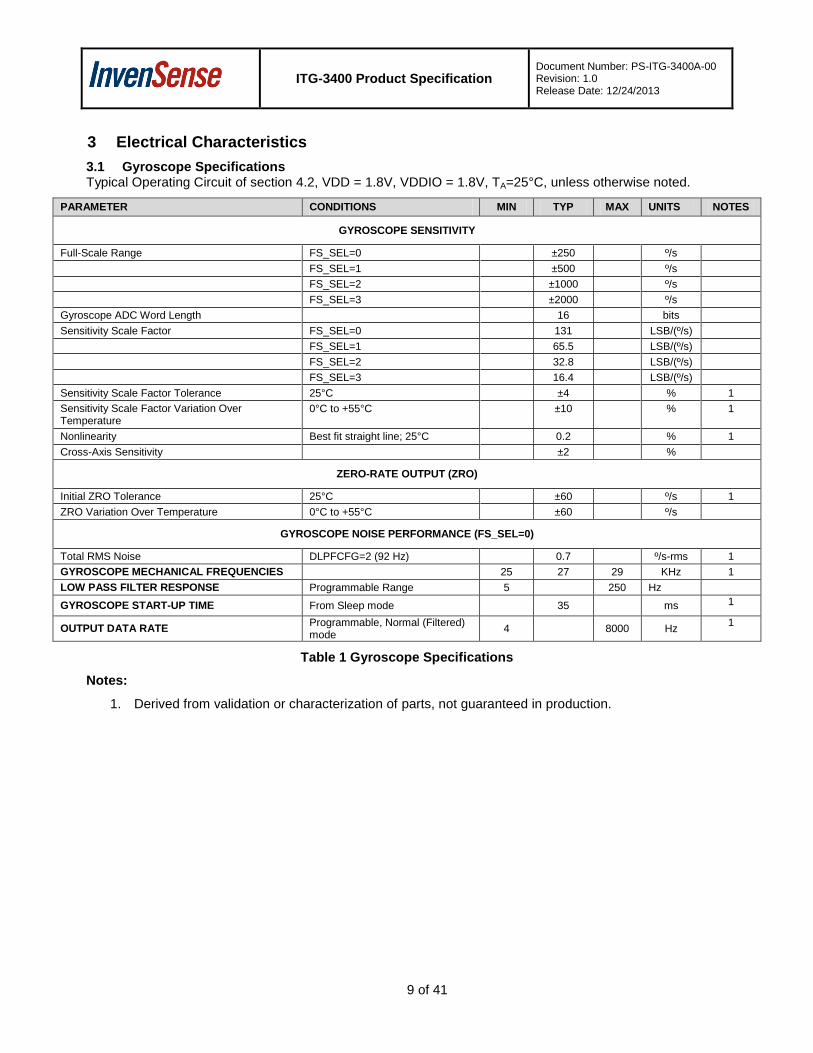
3 Electrical Characteristics
3.1 Gyroscope Specifications Typical Operating Circuit of section 4.2, VDD = 1.8V, VDDIO = 1.8V, TA=25°C, unless otherwise noted.
PARAMETER CONDITIONS MIN TYP MAX UNITS NOTES
GYROSCOPE SENSITIVITY
Full-Scale Range FS_SEL=0 ±250 º/s
FS_SEL=1 ±500 º/s
FS_SEL=2 ±1000 º/s
FS_SEL=3 ±2000 º/s
Gyroscope ADC Word Length 16 bits
Sensitivity Scale Factor FS_SEL=0 131 LSB/(º/s)
FS_SEL=1 65.5 LSB/(º/s)
FS_SEL=2 32.8 LSB/(º/s)
FS_SEL=3 16.4 LSB/(º/s)
Sensitivity Scale Factor Tolerance 25°C ±4 % 1
Sensitivity Scale Factor Variation Over Temperature
0°C to +55°C ±10 % 1
Nonlinearity Best fit straight line; 25°C 0.2 % 1
Cross-Axis Sensitivity ±2 %
ZERO-RATE OUTPUT (ZRO)
Initial ZRO Tolerance 25°C ±60 º/s 1
ZRO Variation Over Temperature 0°C to +55°C ±60 º/s
GYROSCOPE NOISE PERFORMANCE (FS_SEL=0)
Total RMS Noise DLPFCFG=2 (92 Hz) 0.7 º/s-rms 1
GYROSCOPE MECHANICAL FREQUENCIES 25 27 29 KHz 1
LOW PASS FILTER RESPONSE Programmable Range 5 250 Hz
GYROSCOPE START-UP TIME From Sleep mode 35 ms 1
OUTPUT DATA RATE Programmable, Normal (Filtered) mode
4 8000 Hz 1
Table 1 Gyroscope Specifications
Notes:
1. Derived from validation or characterization of parts, not guaranteed in production.
ITG-3400 Product Specification Document Number: PS-ITG-3400A-00 Revision: 1.0 Release Date: 12/24/2013
10 of 41
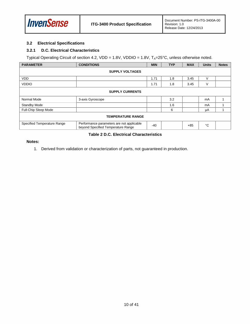
3.2 Electrical Specifications
3.2.1 D.C. Electrical Characteristics
Typical Operating Circuit of section 4.2, VDD = 1.8V, VDDIO = 1.8V, TA=25°C, unless otherwise noted.
PARAMETER CONDITIONS MIN TYP MAX Units Notes
SUPPLY VOLTAGES
VDD 1.71 1.8 3.45 V
VDDIO 1.71 1.8 3.45 V
SUPPLY CURRENTS
Normal Mode 3-axis Gyroscope 3.2 mA 1
Standby Mode 1.6 mA 1
Full-Chip Sleep Mode 6 µA 1
TEMPERATURE RANGE
Specified Temperature Range Performance parameters are not applicable beyond Specified Temperature Range
-40 +85 °C
Table 2 D.C. Electrical Characteristics
Notes:
1. Derived from validation or characterization of parts, not guaranteed in production.
ITG-3400 Product Specification Document Number: PS-ITG-3400A-00 Revision: 1.0 Release Date: 12/24/2013
11 of 41
3.2.2 A.C. Electrical Characteristics
Typical Operating Circuit of section 4.2, VDD = 1.8V, VDDIO = 1.8V, TA=25°C, unless otherwise noted.
Parameter Conditions MIN TYP MAX Units NOTES
SUPPLIES
Supply Ramp Time Monotonic ramp. Ramp rate is 10% to 90% of the final value
0.1 100 ms
1
TEMPERATURE SENSOR
Operating Range Ambient -40 85 °C
1 Sensitivity Untrimmed 333.87 LSB/°C
Room Temp Offset 21°C 0 LSB
Power-On RESET
Supply Ramp Time (TRAMP) Valid power-on RESET 0.01 20 100 ms 1
Start-up time for register read/write From power-up 11 100 ms 1
I2C ADDRESS
AD0 = 0 AD0 = 1
1101000 1101001
DIGITAL INPUTS (SYNC, AD0, SCLK, SDI, CS)
VIH, High Level Input Voltage 0.7*VDDIO V
1 VIL, Low Level Input Voltage 0.3*VDDIO V
CI, Input Capacitance < 10 pF
DIGITAL OUTPUT (SDO, INT)
VOH, High Level Output Voltage RLOAD=1MΩ; 0.9*VDDIO V
1
VOL1, LOW-Level Output Voltage RLOAD=1MΩ; 0.1*VDDIO V
VOL.INT1, INT Low-Level Output Voltage OPEN=1, 0.3mA sink
Current
0.1 V
Output Leakage Current OPEN=1 100 nA
tINT, INT Pulse Width LATCH_INT_EN=0 50 µs
I2C I/O (SCL, SDA)
VIL, LOW Level Input Voltage -0.5V 0.3*VDDIO V
1
VIH, HIGH-Level Input Voltage 0.7*VDDIO VDDIO + 0.5V
V
Vhys, Hysteresis 0.1*VDDIO V
VOL, LOW-Level Output Voltage 3mA sink current 0 0.4 V
IOL, LOW-Level Output Current VOL=0.4V
VOL=0.6V
3 6
mA mA
Output Leakage Current 100 nA
tof, Output Fall Time from VIHmax to VILmax Cb bus capacitance in pf 20+0.1Cb 250 ns
INTERNAL CLOCK SOURCE
Sample Rate
Fchoice=0,1,2 SMPLRT_DIV=0
32 kHz
Fchoice=3; DLPFCFG=0 or 7 SMPLRT_DIV=0
8 kHz
ITG-3400 Product Specification Document Number: PS-ITG-3400A-00 Revision: 1.0 Release Date: 12/24/2013
12 of 41
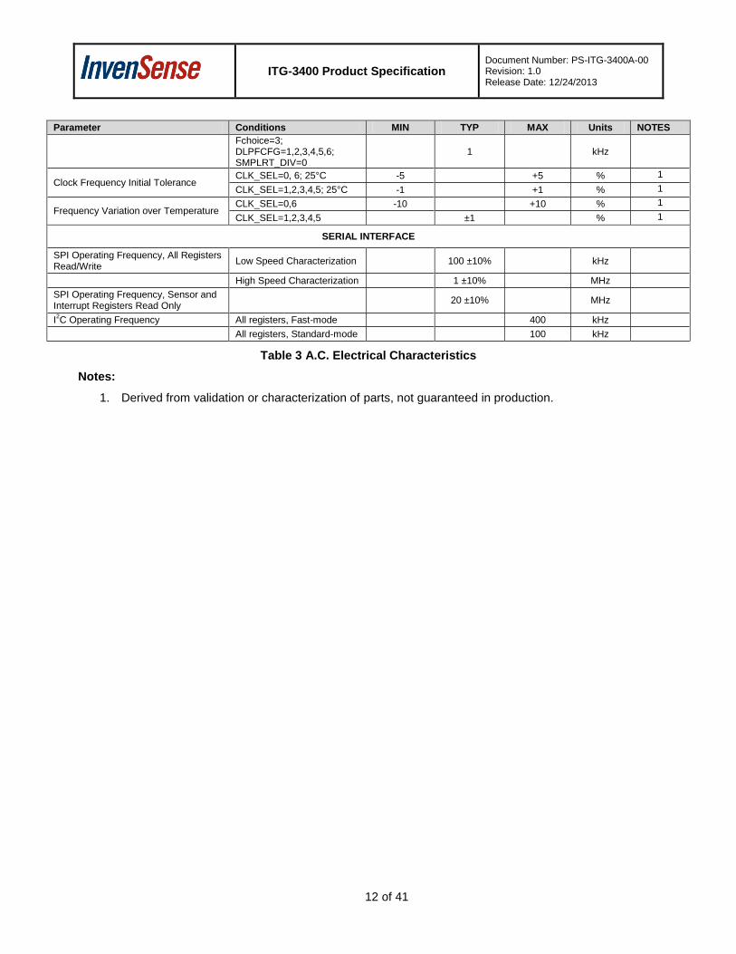
Parameter Conditions MIN TYP MAX Units NOTES
Fchoice=3; DLPFCFG=1,2,3,4,5,6; SMPLRT_DIV=0
1 kHz
Clock Frequency Initial Tolerance CLK_SEL=0, 6; 25°C -5 +5 % 1
CLK_SEL=1,2,3,4,5; 25°C -1 +1 % 1
Frequency Variation over Temperature CLK_SEL=0,6 -10 +10 % 1
CLK_SEL=1,2,3,4,5 ±1 % 1
SERIAL INTERFACE
SPI Operating Frequency, All Registers Read/Write
Low Speed Characterization
100 ±10% kHz
High Speed Characterization 1 ±10% MHz
SPI Operating Frequency, Sensor and Interrupt Registers Read Only
20 ±10% MHz
I2C Operating Frequency All registers, Fast-mode 400 kHz
All registers, Standard-mode 100 kHz
Table 3 A.C. Electrical Characteristics
Notes:
1. Derived from validation or characterization of parts, not guaranteed in production.
ITG-3400 Product Specification Document Number: PS-ITG-3400A-00 Revision: 1.0 Release Date: 12/24/2013
13 of 41
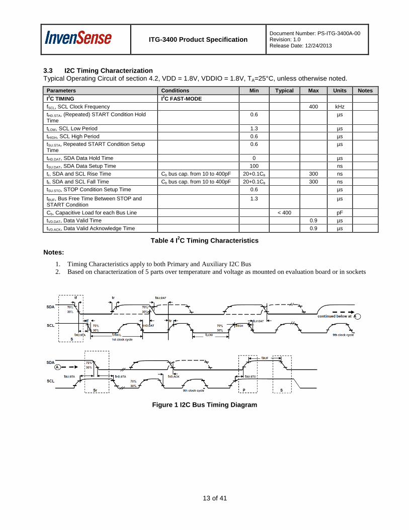
3.3 I2C Timing Characterization Typical Operating Circuit of section 4.2, VDD = 1.8V, VDDIO = 1.8V, TA=25°C, unless otherwise noted.
Parameters Conditions Min Typical Max Units Notes
I2C TIMING I
2C FAST-MODE
fSCL, SCL Clock Frequency 400 kHz
tHD.STA, (Repeated) START Condition Hold Time
0.6 µs
tLOW, SCL Low Period 1.3 µs
tHIGH, SCL High Period 0.6 µs
tSU.STA, Repeated START Condition Setup Time
0.6 µs
tHD.DAT, SDA Data Hold Time 0 µs
tSU.DAT, SDA Data Setup Time 100 ns
tr, SDA and SCL Rise Time Cb bus cap. from 10 to 400pF 20+0.1Cb 300 ns
tf, SDA and SCL Fall Time Cb bus cap. from 10 to 400pF 20+0.1Cb 300 ns
tSU.STO, STOP Condition Setup Time 0.6 µs
tBUF, Bus Free Time Between STOP and START Condition
1.3 µs
Cb, Capacitive Load for each Bus Line < 400 pF
tVD.DAT, Data Valid Time 0.9 µs
tVD.ACK, Data Valid Acknowledge Time 0.9 µs
Table 4 I2C Timing Characteristics
Notes:
1. Timing Characteristics apply to both Primary and Auxiliary I2C Bus
2. Based on characterization of 5 parts over temperature and voltage as mounted on evaluation board or in sockets
Figure 1 I2C Bus Timing Diagram
ITG-3400 Product Specification Document Number: PS-ITG-3400A-00 Revision: 1.0 Release Date: 12/24/2013
14 of 41
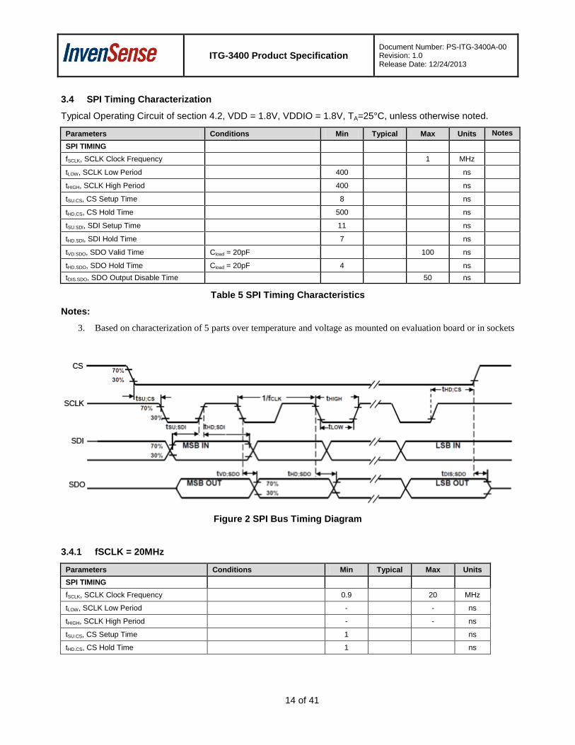
3.4 SPI Timing Characterization
Typical Operating Circuit of section 4.2, VDD = 1.8V, VDDIO = 1.8V, TA=25°C, unless otherwise noted.
Parameters Conditions Min Typical Max Units Notes
SPI TIMING
fSCLK, SCLK Clock Frequency
1 MHz
tLOW, SCLK Low Period
400
ns
tHIGH, SCLK High Period
400
ns
tSU.CS, CS Setup Time
8
ns
tHD.CS, CS Hold Time
500
ns
tSU.SDI, SDI Setup Time
11
ns
tHD.SDI, SDI Hold Time
7
ns
tVD.SDO, SDO Valid Time Cload = 20pF
100 ns
tHD.SDO, SDO Hold Time Cload = 20pF 4
ns
tDIS.SDO, SDO Output Disable Time
50 ns
Table 5 SPI Timing Characteristics
Notes:
3. Based on characterization of 5 parts over temperature and voltage as mounted on evaluation board or in sockets
Figure 2 SPI Bus Timing Diagram
3.4.1 fSCLK = 20MHz
Parameters Conditions Min Typical Max Units
SPI TIMING
fSCLK, SCLK Clock Frequency 0.9 20 MHz
tLOW, SCLK Low Period - - ns
tHIGH, SCLK High Period - - ns
tSU.CS, CS Setup Time 1 ns
tHD.CS, CS Hold Time 1 ns
ITG-3400 Product Specification Document Number: PS-ITG-3400A-00 Revision: 1.0 Release Date: 12/24/2013
15 of 41
tSU.SDI, SDI Setup Time 0 ns
tHD.SDI, SDI Hold Time 1 ns
tVD.SDO, SDO Valid Time Cload = 20pF 25 ns
tDIS.SDO, SDO Output Disable Time 25 ns
Table 6 fCLK = 20MHz
Notes:
1. Based on characterization of 5 parts over temperature and voltage as mounted on evaluation board or in sockets
3.5 Absolute Maximum Ratings
Stress above those listed as “Absolute Maximum Ratings” may cause permanent damage to the device. These are stress ratings only and functional operation of the device at these conditions is not implied. Exposure to the absolute maximum ratings conditions for extended periods may affect device reliability.
Parameter Rating
Supply Voltage, VDD -0.5V to +4V
Supply Voltage, VDDIO -0.5V to +4V
PLLFILT -0.5V to 2V
Input Voltage Level (AD0, SYNC, INT, SCL, SDA) -0.5V to VDD + 0.5V
Operating Temperature Range -40°C to +85°C
Storage Temperature Range -40°C to +125°C
Electrostatic Discharge (ESD) Protection 2kV (HBM);
250V (MM)
Latch-up JEDEC Class II (2),125°C
±100mA
Table 7 Absolute Maximum Ratings
ITG-3400 Product Specification Document Number: PS-ITG-3400A-00 Revision: 1.0 Release Date: 12/24/2013
16 of 41
4 Applications Information
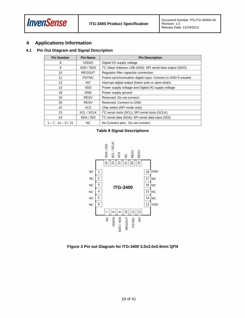
4.1 Pin Out Diagram and Signal Description
Pin Number Pin Name Pin Description
8 VDDIO Digital I/O supply voltage
9 AD0 / SDO I2C Slave Address LSB (AD0); SPI serial data output (SDO)
10 REGOUT Regulator filter capacitor connection
11 FSYNC Frame synchronization digital input. Connect to GND if unused.
12 INT Interrupt digital output (totem pole or open-drain)
13 VDD Power supply voltage and Digital I/O supply voltage
18 GND Power supply ground
19 RESV Reserved. Do not connect.
20 RESV Reserved. Connect to GND.
22 nCS Chip select (SPI mode only)
23 SCL / SCLK I2C serial clock (SCL); SPI serial clock (SCLK)
24 SDA / SDI I2C serial data (SDA); SPI serial data input (SDI)
1 – 7, 14 – 17, 21 NC No Connect pins. Do not connect.
Table 8 Signal Descriptions
NC
VD
DIO
SD
O / A
D0
RE
GO
UT
FS
YN
C
INT
GND
SC
L / S
CL
K
nC
S
RE
SV
VDD
SD
A / S
DI
NC
NC
RE
SV
NC
NC
NC
NC
NC
NC
NC
NC
NCITG-3400
1
2
3
4
5
6 13
18
17
16
15
14
7 8 9 10
11
12
24
23
22
21
20
19
Figure 3 Pin out Diagram for ITG-3400 3.0x3.0x0.9mm QFN
ITG-3400 Product Specification Document Number: PS-ITG-3400A-00 Revision: 1.0 Release Date: 12/24/2013
17 of 41
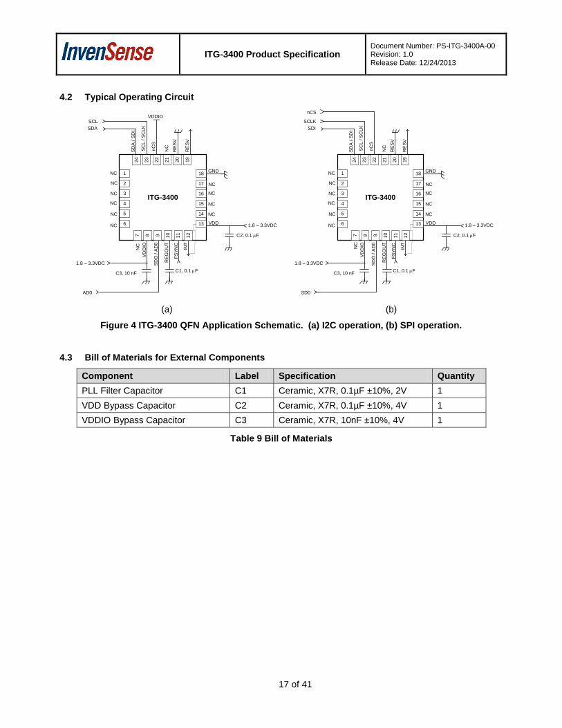
4.2 Typical Operating Circuit
VD
DIO
SD
O /
AD
0
RE
GO
UT
FS
YN
C
INT
GND
SC
L / S
CL
K
nC
S
RE
SV
VDD
SD
A / S
DI
NC
1.8 – 3.3VDC
C2, 0.1 mF
C3, 10 nF
1.8 – 3.3VDC
SCLVDDIO
SDA
AD0
C1, 0.1 mF
RE
SV
NC
NC
NC
NC
NC
NC
NC
NC
NCITG-3400
1
2
3
4
5
6 13
18
17
16
15
14
7 8 9 10
11
12
24
23
22
21
20
19
NC
NC
VD
DIO
SD
O /
AD
0
RE
GO
UT
FS
YN
C
INT
GND
SC
L / S
CL
K
nC
S
RE
SV
VDD
SD
A / S
DI
NC
1.8 – 3.3VDC
C2, 0.1 mF
C3, 10 nF
1.8 – 3.3VDC
SCLK
SDI
SD0
C1, 0.1 mF
RE
SV
NC
NC
NC
NC
NC
NC
NC
NC
NCITG-3400
1
2
3
4
5
6 13
18
17
16
15
14
7 8 9 10
11
12
24
23
22
21
20
19
nCS
NC
NC
(a) (b)
Figure 4 ITG-3400 QFN Application Schematic. (a) I2C operation, (b) SPI operation.
4.3 Bill of Materials for External Components
Component Label Specification Quantity
PLL Filter Capacitor C1 Ceramic, X7R, 0.1µF ±10%, 2V 1
VDD Bypass Capacitor C2 Ceramic, X7R, 0.1µF ±10%, 4V 1
VDDIO Bypass Capacitor C3 Ceramic, X7R, 10nF ±10%, 4V 1
Table 9 Bill of Materials
ITG-3400 Product Specification Document Number: PS-ITG-3400A-00 Revision: 1.0 Release Date: 12/24/2013
18 of 41
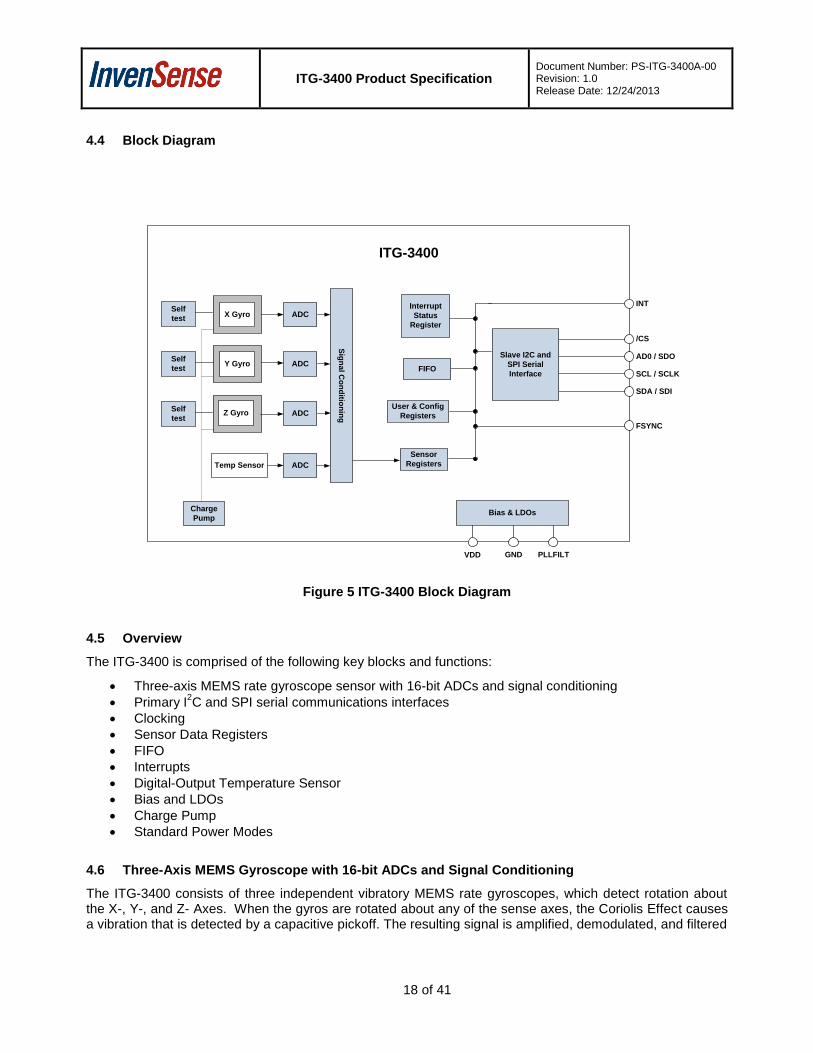
4.4 Block Diagram
ITG-3400
Charge
Pump
/CS
AD0 / SDO
SCL / SCLK
SDA / SDI
Temp Sensor ADC
ADCZ Gyro
ADCY Gyro
FSYNC
Slave I2C and
SPI Serial
Interface
INTInterrupt
Status
Register
VDD
Bias & LDOs
GND PLLFILT
ADCX Gyro
Sig
na
l Co
nd
ition
ing
FIFO
User & Config
Registers
Sensor
Registers
Self
test
Self
test
Self
test
Figure 5 ITG-3400 Block Diagram
4.5 Overview
The ITG-3400 is comprised of the following key blocks and functions:
Three-axis MEMS rate gyroscope sensor with 16-bit ADCs and signal conditioning
Primary I2C and SPI serial communications interfaces
Clocking
Sensor Data Registers
FIFO
Interrupts
Digital-Output Temperature Sensor
Bias and LDOs
Charge Pump
Standard Power Modes
4.6 Three-Axis MEMS Gyroscope with 16-bit ADCs and Signal Conditioning
The ITG-3400 consists of three independent vibratory MEMS rate gyroscopes, which detect rotation about the X-, Y-, and Z- Axes. When the gyros are rotated about any of the sense axes, the Coriolis Effect causes a vibration that is detected by a capacitive pickoff. The resulting signal is amplified, demodulated, and filtered
ITG-3400 Product Specification Document Number: PS-ITG-3400A-00 Revision: 1.0 Release Date: 12/24/2013
19 of 41
to produce a voltage that is proportional to the angular rate. This voltage is digitized using individual on-chip 16-bit Analog-to-Digital Converters (ADCs) to sample each axis. The full-scale range of the gyro sensors may be digitally programmed to ±250, ±500, ±1000, or ±2000 degrees per second (dps). The ADC sample rate is programmable from 8,000 samples per second, down to 3.9 samples per second, and user-selectable low-pass filters enable a wide range of cut-off frequencies.
4.7 I2C and SPI Serial Communications Interfaces
The ITG-3400 communicates to a system processor using either a SPI or an I2C serial interface. The ITG-
3400 always acts as a slave when communicating to the system processor. The LSB of the of the I2C slave
address is set by pin 4 (AD0).
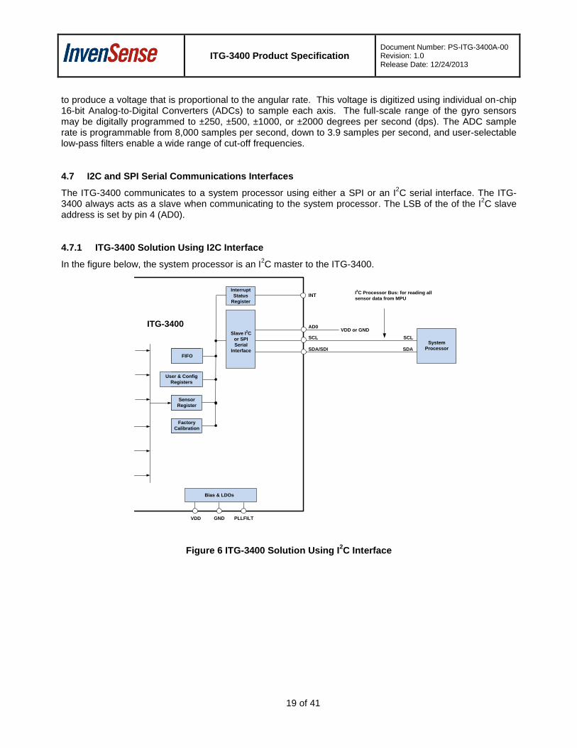
4.7.1 ITG-3400 Solution Using I2C Interface
In the figure below, the system processor is an I2C master to the ITG-3400.
ITG-3400 AD0
SCL
SDA/SDI
Interrupt
Status
Register
INT
VDD
Bias & LDOs
GND PLLFILT
FIFO
User & Config
Registers
Sensor
Register
Factory
Calibration
Slave I2C
or SPI
Serial
Interface
System
Processor
SCL
SDA
VDD or GND
I2C Processor Bus: for reading all
sensor data from MPU
Figure 6 ITG-3400 Solution Using I2C Interface
ITG-3400 Product Specification Document Number: PS-ITG-3400A-00 Revision: 1.0 Release Date: 12/24/2013
20 of 41
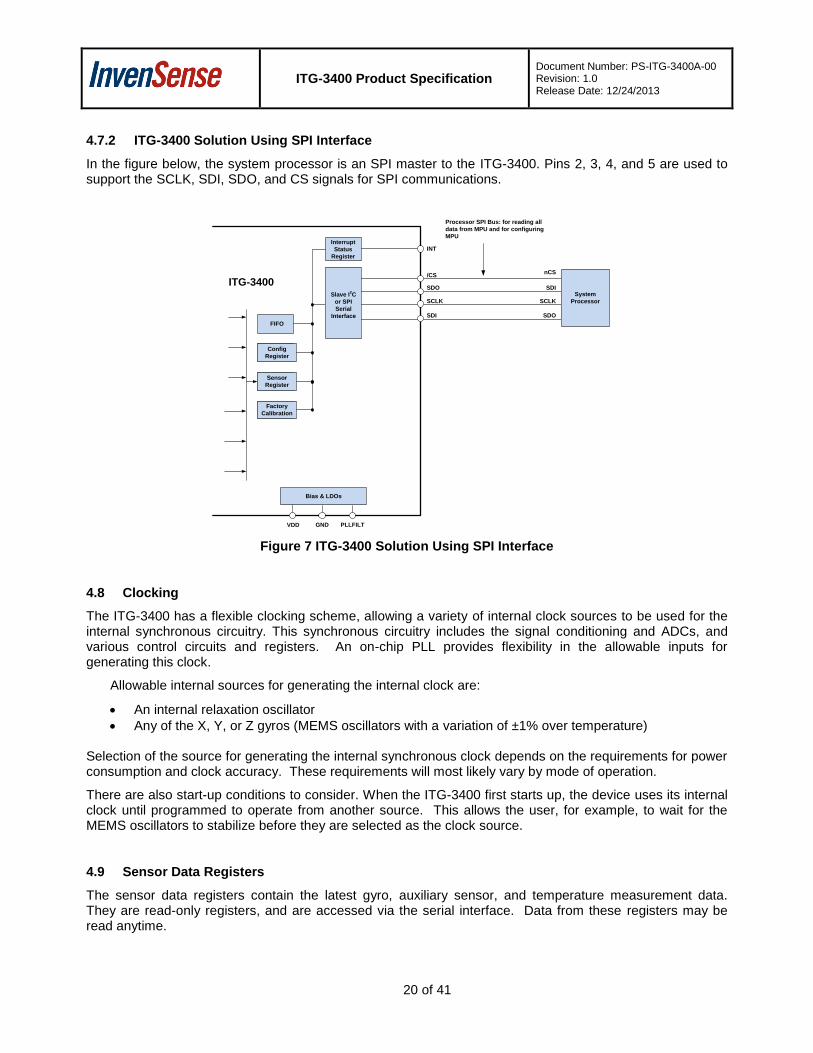
4.7.2 ITG-3400 Solution Using SPI Interface
In the figure below, the system processor is an SPI master to the ITG-3400. Pins 2, 3, 4, and 5 are used to support the SCLK, SDI, SDO, and CS signals for SPI communications.
ITG-3400SDO
SCLK
SDI
Interrupt
Status
Register
INT
FIFO
Config
Register
Sensor
Register
Factory
Calibration
/CS
Slave I2C
or SPI
Serial
Interface
System
Processor
SDI
SCLK
SDO
nCS
Processor SPI Bus: for reading all
data from MPU and for configuring
MPU
VDD
Bias & LDOs
GND PLLFILT
Figure 7 ITG-3400 Solution Using SPI Interface
4.8 Clocking
The ITG-3400 has a flexible clocking scheme, allowing a variety of internal clock sources to be used for the internal synchronous circuitry. This synchronous circuitry includes the signal conditioning and ADCs, and various control circuits and registers. An on-chip PLL provides flexibility in the allowable inputs for generating this clock.
Allowable internal sources for generating the internal clock are:
An internal relaxation oscillator
Any of the X, Y, or Z gyros (MEMS oscillators with a variation of ±1% over temperature)
Selection of the source for generating the internal synchronous clock depends on the requirements for power consumption and clock accuracy. These requirements will most likely vary by mode of operation.
There are also start-up conditions to consider. When the ITG-3400 first starts up, the device uses its internal clock until programmed to operate from another source. This allows the user, for example, to wait for the MEMS oscillators to stabilize before they are selected as the clock source.
4.9 Sensor Data Registers
The sensor data registers contain the latest gyro, auxiliary sensor, and temperature measurement data. They are read-only registers, and are accessed via the serial interface. Data from these registers may be read anytime.
ITG-3400 Product Specification Document Number: PS-ITG-3400A-00 Revision: 1.0 Release Date: 12/24/2013
21 of 41
4.10 FIFO
The ITG-3400 contains a 4096-byte FIFO register that is accessible via the Serial Interface. The FIFO configuration register determines which data is written into the FIFO. Possible choices include gyro data, temperature readings, auxiliary sensor readings, and SYNC input. A FIFO counter keeps track of how many bytes of valid data are contained in the FIFO. The FIFO register supports burst reads. The interrupt function may be used to determine when new data is available.
For further information regarding the FIFO, please refer to the ITG-3400 Register Map and Register Descriptions document.
4.11 Interrupts
Interrupt functionality is configured via the Interrupt Configuration register. Items that are configurable include the INT pin configuration, the interrupt latching and clearing method, and triggers for the interrupt. Items that can trigger an interrupt are (1) Clock generator locked to new reference oscillator (used when switching clock sources); and (2) new data is available to be read (from the FIFO and Data registers). The interrupt status can be read from the Interrupt Status register.
For further information regarding interrupts, please refer to the ITG-3400 Register Map and Register Descriptions document.
4.12 Digital-Output Temperature Sensor
An on-chip temperature sensor and ADC are used to measure the ITG-3400 die temperature. The readings from the ADC can be read from the FIFO or the Sensor Data registers.
4.13 Bias and LDOs
The bias and LDO section generates the internal supply and the reference voltages and currents required by the ITG-3400. Its two inputs are an unregulated VDD and a VDDIO logic reference supply voltage. The LDO output is bypassed by a capacitor at PLLFILT. For further details on the capacitor, please refer to the Bill of Materials for External Components.
4.14 Charge Pump
An on-chip charge pump generates the high voltage required for the MEMS oscillators.
4.15 Standard Power Modes
The following table lists the user-accessible power modes for ITG-3400.
Mode Name Gyro
1 Sleep Mode Off
2 Standby Mode Drive On
5 Gyroscope Mode On

ITG-3400 Product Specification Document Number: PS-ITG-3400A-00 Revision: 1.0 Release Date: 12/24/2013
22 of 41
Table 10 Standard Power Modes for ITG-3400
Notes: 1. Power consumption for individual modes can be found in section 3.2.1.
ITG-3400 Product Specification Document Number: PS-ITG-3400A-00 Revision: 1.0 Release Date: 12/24/2013
23 of 41
5 Programmable Interrupts
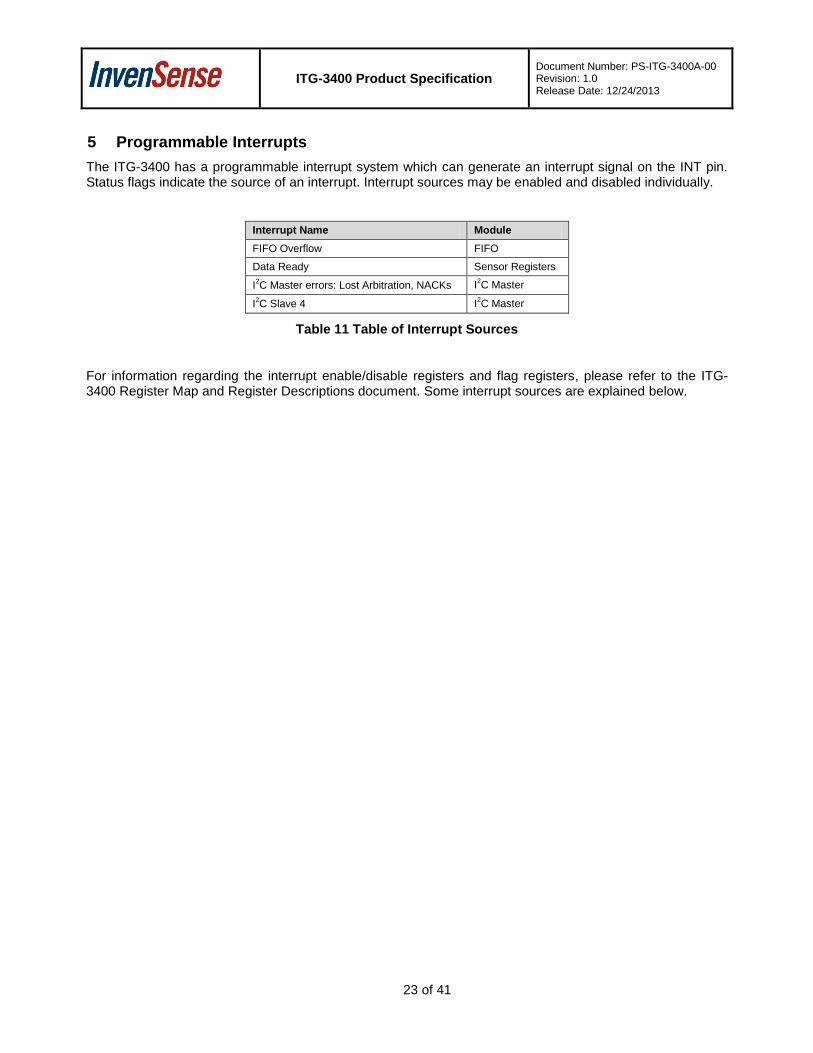
The ITG-3400 has a programmable interrupt system which can generate an interrupt signal on the INT pin. Status flags indicate the source of an interrupt. Interrupt sources may be enabled and disabled individually.
Interrupt Name Module
FIFO Overflow FIFO
Data Ready Sensor Registers
I2C Master errors: Lost Arbitration, NACKs I
2C Master
I2C Slave 4 I
2C Master
Table 11 Table of Interrupt Sources
For information regarding the interrupt enable/disable registers and flag registers, please refer to the ITG-3400 Register Map and Register Descriptions document. Some interrupt sources are explained below.
ITG-3400 Product Specification Document Number: PS-ITG-3400A-00 Revision: 1.0 Release Date: 12/24/2013
24 of 41
6 Digital Interface
6.1 I2C and SPI Serial Interfaces
The internal registers and memory of the ITG-3400 can be accessed using either I2C at 400 kHz or SPI at
1MHz. SPI operates in four-wire mode.
Pin Number Pin Name Pin Description
8 VDDIO Digital I/O supply voltage.
9 AD0 / SDO I2C Slave Address LSB (AD0); SPI serial data output (SDO)
23 SCL / SCLK I2C serial clock (SCL); SPI serial clock (SCLK)
24 SDA / SDI I2C serial data (SDA); SPI serial data input (SDI)
Table 12 Serial Interface
Note:
To prevent switching into I2C mode when using SPI, the I
2C interface should be disabled by setting the
I2C_IF_DIS configuration bit. Setting this bit should be performed immediately after waiting for the time specified by the “Start-Up Time for Register Read/Write” in Section 6.3.
For further information regarding the I2C_IF_DIS bit, please refer to the ITG-3400 Register Map and Register Descriptions document.
6.2 I2C Interface
I2C is a two-wire interface comprised of the signals serial data (SDA) and serial clock (SCL). In general, the
lines are open-drain and bi-directional. In a generalized I2C interface implementation, attached devices can
be a master or a slave. The master device puts the slave address on the bus, and the slave device with the matching address acknowledges the master.
The ITG-3400 always operates as a slave device when communicating to the system processor, which thus acts as the master. SDA and SCL lines typically need pull-up resistors to VDD. The maximum bus speed is 400 kHz.
The slave address of the ITG-3400 is b110111X which is 7 bits long. The LSB bit of the 7 bit address is determined by the logic level on pin AD0. This allows two ITG-3400s to be connected to the same I
2C bus.
When used in this configuration, the address of the one of the devices should be b1101110 (pin AD0 is logic low) and the address of the other should be b1101111 (pin AD0 is logic high).
6.3 I2C Communications Protocol
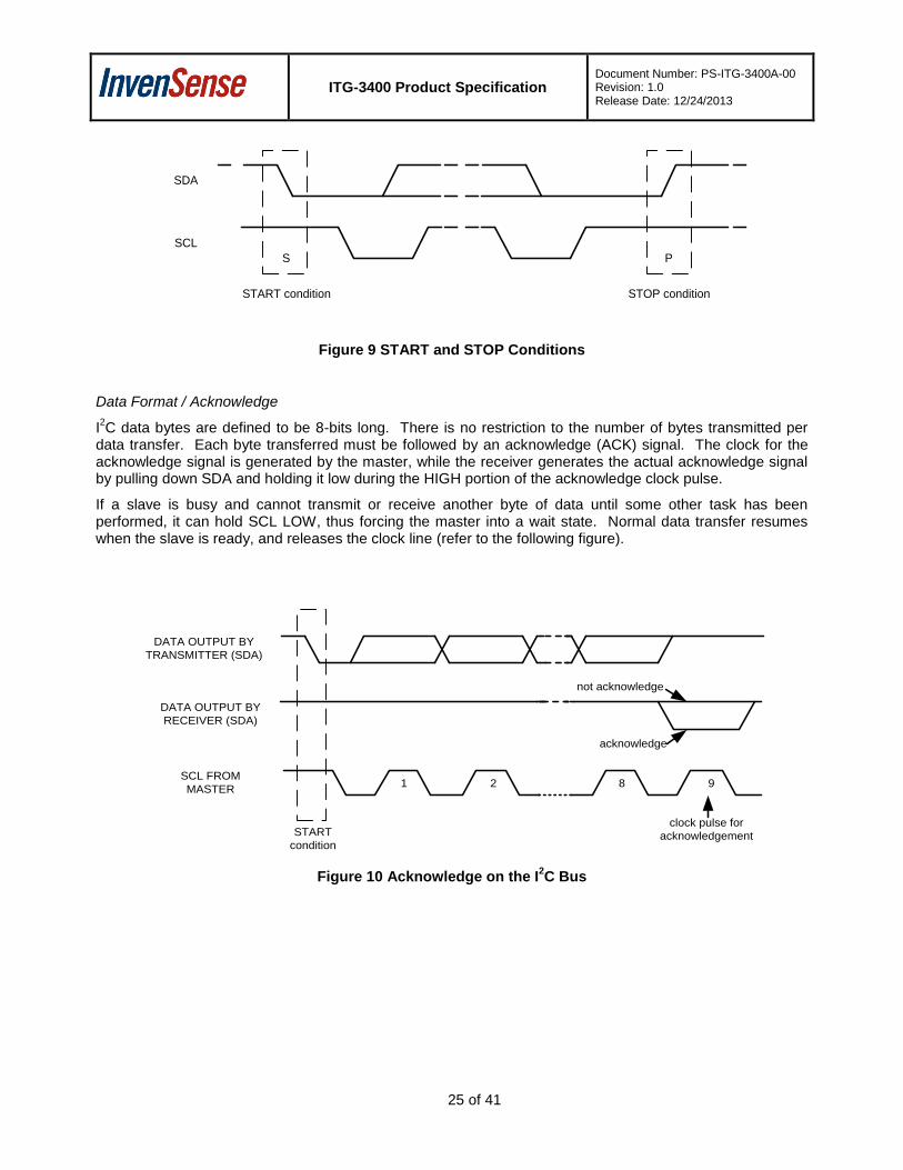
START (S) and STOP (P) Conditions
Communication on the I2C bus starts when the master puts the START condition (S) on the bus, which is
defined as a HIGH-to-LOW transition of the SDA line while SCL line is HIGH (see figure below). The bus is considered to be busy until the master puts a STOP condition (P) on the bus, which is defined as a LOW to HIGH transition on the SDA line while SCL is HIGH (see figure below).
Additionally, the bus remains busy if a repeated START (Sr) is generated instead of a STOP condition.
ITG-3400 Product Specification Document Number: PS-ITG-3400A-00 Revision: 1.0 Release Date: 12/24/2013
25 of 41
SDA
SCL
S
START condition STOP condition
P
Figure 9 START and STOP Conditions
Data Format / Acknowledge
I2C data bytes are defined to be 8-bits long. There is no restriction to the number of bytes transmitted per
data transfer. Each byte transferred must be followed by an acknowledge (ACK) signal. The clock for the acknowledge signal is generated by the master, while the receiver generates the actual acknowledge signal by pulling down SDA and holding it low during the HIGH portion of the acknowledge clock pulse.
If a slave is busy and cannot transmit or receive another byte of data until some other task has been performed, it can hold SCL LOW, thus forcing the master into a wait state. Normal data transfer resumes when the slave is ready, and releases the clock line (refer to the following figure).
DATA OUTPUT BY
TRANSMITTER (SDA)
DATA OUTPUT BY
RECEIVER (SDA)
SCL FROM
MASTER
START
condition
clock pulse for
acknowledgement
acknowledge
not acknowledge
1 2 8 9
Figure 10 Acknowledge on the I2C Bus
ITG-3400 Product Specification Document Number: PS-ITG-3400A-00 Revision: 1.0 Release Date: 12/24/2013
26 of 41
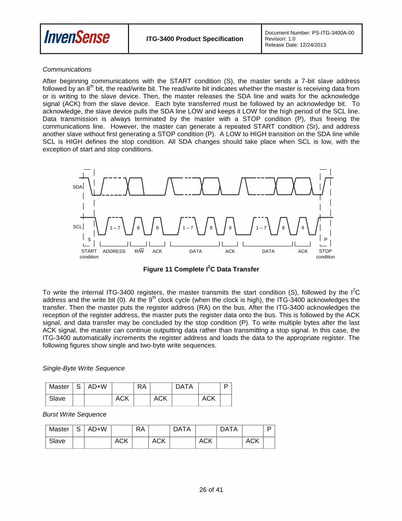
Communications
After beginning communications with the START condition (S), the master sends a 7-bit slave address followed by an 8
th bit, the read/write bit. The read/write bit indicates whether the master is receiving data from
or is writing to the slave device. Then, the master releases the SDA line and waits for the acknowledge signal (ACK) from the slave device. Each byte transferred must be followed by an acknowledge bit. To acknowledge, the slave device pulls the SDA line LOW and keeps it LOW for the high period of the SCL line. Data transmission is always terminated by the master with a STOP condition (P), thus freeing the communications line. However, the master can generate a repeated START condition (Sr), and address another slave without first generating a STOP condition (P). A LOW to HIGH transition on the SDA line while SCL is HIGH defines the stop condition. All SDA changes should take place when SCL is low, with the exception of start and stop conditions.
SDA
START
condition
SCL
ADDRESS R/W ACK DATA ACK DATA ACK STOP
condition
S P
1 – 7 8 9 1 – 7 8 9 1 – 7 8 9
Figure 11 Complete I2C Data Transfer
To write the internal ITG-3400 registers, the master transmits the start condition (S), followed by the I2C
address and the write bit (0). At the 9th clock cycle (when the clock is high), the ITG-3400 acknowledges the
transfer. Then the master puts the register address (RA) on the bus. After the ITG-3400 acknowledges the reception of the register address, the master puts the register data onto the bus. This is followed by the ACK signal, and data transfer may be concluded by the stop condition (P). To write multiple bytes after the last ACK signal, the master can continue outputting data rather than transmitting a stop signal. In this case, the ITG-3400 automatically increments the register address and loads the data to the appropriate register. The following figures show single and two-byte write sequences.
Single-Byte Write Sequence
Burst Write Sequence
Master S AD+W RA DATA P
Slave ACK ACK ACK
Master S AD+W RA DATA DATA P
Slave ACK ACK ACK ACK
ITG-3400 Product Specification Document Number: PS-ITG-3400A-00 Revision: 1.0 Release Date: 12/24/2013
27 of 41
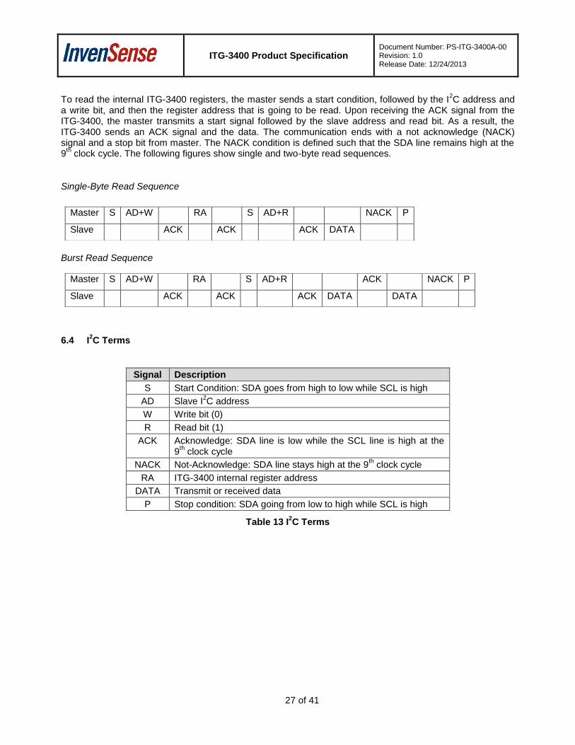
To read the internal ITG-3400 registers, the master sends a start condition, followed by the I2C address and
a write bit, and then the register address that is going to be read. Upon receiving the ACK signal from the ITG-3400, the master transmits a start signal followed by the slave address and read bit. As a result, the ITG-3400 sends an ACK signal and the data. The communication ends with a not acknowledge (NACK) signal and a stop bit from master. The NACK condition is defined such that the SDA line remains high at the 9
th clock cycle. The following figures show single and two-byte read sequences.
Single-Byte Read Sequence
Burst Read Sequence
6.4 I2C Terms
Signal Description
S Start Condition: SDA goes from high to low while SCL is high
AD Slave I2C address
W Write bit (0)
R Read bit (1)
ACK Acknowledge: SDA line is low while the SCL line is high at the 9
th clock cycle
NACK Not-Acknowledge: SDA line stays high at the 9th clock cycle
RA ITG-3400 internal register address
DATA Transmit or received data
P Stop condition: SDA going from low to high while SCL is high
Table 13 I2C Terms
Master S AD+W RA S AD+R NACK P
Slave ACK ACK ACK DATA
Master S AD+W RA S AD+R ACK NACK P
Slave ACK ACK ACK DATA DATA
ITG-3400 Product Specification Document Number: PS-ITG-3400A-00 Revision: 1.0 Release Date: 12/24/2013
28 of 41
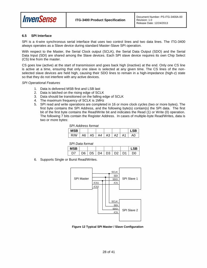
6.5 SPI Interface
SPI is a 4-wire synchronous serial interface that uses two control lines and two data lines. The ITG-3400 always operates as a Slave device during standard Master-Slave SPI operation.
With respect to the Master, the Serial Clock output (SCLK), the Serial Data Output (SDO) and the Serial Data Input (SDI) are shared among the Slave devices. Each SPI slave device requires its own Chip Select (CS) line from the master.
CS goes low (active) at the start of transmission and goes back high (inactive) at the end. Only one CS line is active at a time, ensuring that only one slave is selected at any given time. The CS lines of the non-selected slave devices are held high, causing their SDO lines to remain in a high-impedance (high-z) state so that they do not interfere with any active devices.
SPI Operational Features
1. Data is delivered MSB first and LSB last 2. Data is latched on the rising edge of SCLK 3. Data should be transitioned on the falling edge of SCLK 4. The maximum frequency of SCLK is 1MHz 5. SPI read and write operations are completed in 16 or more clock cycles (two or more bytes). The
first byte contains the SPI Address, and the following byte(s) contain(s) the SPI data. The first bit of the first byte contains the Read/Write bit and indicates the Read (1) or Write (0) operation. The following 7 bits contain the Register Address. In cases of multiple-byte Read/Writes, data is two or more bytes:
SPI Address format
MSB LSB
R/W A6 A5 A4 A3 A2 A1 A0
SPI Data format
MSB LSB
D7 D6 D5 D4 D3 D2 D1 D0
6. Supports Single or Burst Read/Writes.
Figure 12 Typical SPI Master / Slave Configuration
SPI Master SPI Slave 1
SPI Slave 2
/CS1
/CS2
SCLK
SDI
SDO
/CS
SCLK
SDI
SDO
/CS
ITG-3400 Product Specification Document Number: PS-ITG-3400A-00 Revision: 1.0 Release Date: 12/24/2013
29 of 41
7 Serial Interface Considerations
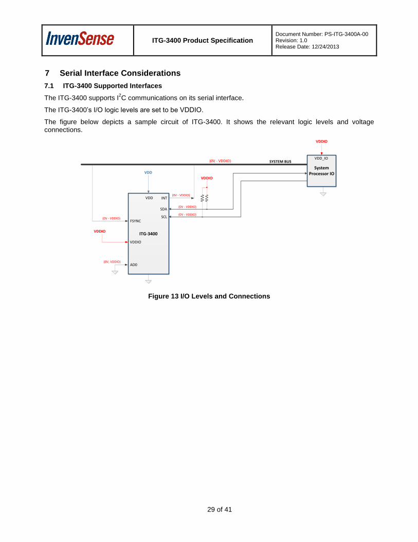
7.1 ITG-3400 Supported Interfaces
The ITG-3400 supports I2C communications on its serial interface.
The ITG-3400’s I/O logic levels are set to be VDDIO.
The figure below depicts a sample circuit of ITG-3400. It shows the relevant logic levels and voltage connections.
ITG-3400
VDD
System Processor IO
SYSTEM BUS
VDDIO
VDDIO
VDD
VDDIO
SCL
SDA
INT
FSYNC
VDDIO
AD0
(0V - VDDIO)
(0V - VDDIO)(0V - VDDIO)
(0V - VDDIO)
(0V - VDDIO)
(0V, VDDIO)
VDD_IO
Figure 13 I/O Levels and Connections

ITG-3400 Product Specification Document Number: PS-ITG-3400A-00 Revision: 1.0 Release Date: 12/24/2013
30 of 41
8 Assembly
This section provides general guidelines for assembling InvenSense Micro Electro-Mechanical Systems (MEMS) gyros packaged in QFN package.
8.1 Orientation of Axes The diagram below shows the orientation of the axes of sensitivity and the polarity of rotation. Note the pin 1 identifier (•) in the figure.
ITG-3400
+Z
+X
+Y
+Z
+Y
+X
Figure 14 Orientation of Axes of Sensitivity and Polarity of Rotation

ITG-3400 Product Specification Document Number: PS-ITG-3400A-00 Revision: 1.0 Release Date: 12/24/2013
31 of 41
8.2 Package Dimensions
24 Lead QFN (3x3x0.9) mm NiPdAu Lead-frame finish
DIMENSIONS IN
MILLIMETERS
SYMBOLS DESCRIPTION MIN NOM MAX
A Package thickness 0.85 0.90 0.95
A1 Lead finger (pad) seating height 0.00 0.02 0.05
b Lead finger (pad) width 0.15 0.20 0.25
c Lead frame (pad) height --- 0.20 REF ---
D Package width 2.90 3.00 3.10
D2 Exposed pad width 1.65 1.70 1.75
E Package length 2.90 3.00 3.10
E2 Exposed pad length 1.49 1.54 1.59
e Lead finger-finger (pad-pad) pitch --- 0.40 ---
f (e-b) Lead-lead (Pad-Pad) space 0.15 0.20 0.25
K Lead (pad) to Exposed Pad Space --- 0.35 REF ---
L Lead (pad) length 0.25 0.30 0.35
R Lead (pad) corner radius 0.075 REF ---
R’ Corner lead (pad) outer radius 0.10 0.11 0.12
R’’ Corner lead (pad) inner radius 0.10 0.11 0.12
s Corner lead-lead (pad-pad) spacing --- 0.25 REF ---
y Lead conformality 0.00 --- 0.075
ITG-3400 Product Specification Document Number: PS-ITG-3400A-00 Revision: 1.0 Release Date: 12/24/2013
32 of 41
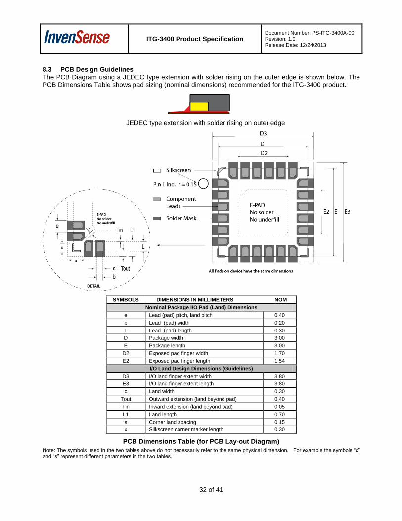
8.3 PCB Design Guidelines The PCB Diagram using a JEDEC type extension with solder rising on the outer edge is shown below. The PCB Dimensions Table shows pad sizing (nominal dimensions) recommended for the ITG-3400 product.
JEDEC type extension with solder rising on outer edge
SYMBOLS DIMENSIONS IN MILLIMETERS NOM
Nominal Package I/O Pad (Land) Dimensions
e Lead (pad) pitch, land pitch 0.40
b Lead (pad) width 0.20
L Lead (pad) length 0.30
D Package width 3.00
E Package length 3.00
D2 Exposed pad finger width 1.70
E2 Exposed pad finger length 1.54
I/O Land Design Dimensions (Guidelines)
D3 I/O land finger extent width 3.80
E3 I/O land finger extent length 3.80
c Land width 0.30
Tout Outward extension (land beyond pad) 0.40
Tin Inward extension (land beyond pad) 0.05
L1 Land length 0.70
s Corner land spacing 0.15
x Silkscreen corner marker length 0.30
PCB Dimensions Table (for PCB Lay-out Diagram)
Note: The symbols used in the two tables above do not necessarily refer to the same physical dimension. For example the symbols “c” and “s” represent different parameters in the two tables.
ITG-3400 Product Specification Document Number: PS-ITG-3400A-00 Revision: 1.0 Release Date: 12/24/2013
33 of 41
8.4 Assembly Precautions
8.4.1 Gyroscope Surface Mount Guidelines
InvenSense MEMS Gyros sense rate of rotation. In addition, gyroscopes sense mechanical stress coming from the printed circuit board (PCB). This PCB stress can be minimized by adhering to certain design rules:
When using MEMS gyroscope components in plastic packages, PCB mounting and assembly can cause package stress. This package stress in turn can affect the output offset and its value over a wide range of temperatures. This stress is caused by the mismatch between the Coefficient of Linear Thermal Expansion (CTE) of the package material and the PCB. Care must be taken to avoid package stress due to mounting.
Traces connected to pads should be as symmetric as possible. Maximizing symmetry and balance for pad connection will help component self alignment and will lead to better control of solder paste reduction after reflow.
Any material used in the surface mount assembly process of the MEMS gyroscope should be free of restricted RoHS elements or compounds. Pb-free solders should be used for assembly.
8.4.2 Exposed Die Pad Precautions
The ITG-3400 has very low active and standby current consumption. There is no electrical connection between the exposed die pad and the internal CMOS circuits. The exposed die pad is not required for heat- sinking, and should not be soldered to the PCB. Underfill is also not recommended. Soldering or adding underfill to the e-pad can induce performance changes due to package thermo-mechanical stress.
8.4.3 Trace Routing
Routing traces or vias under the gyro package such that they run under the exposed die pad is prohibited. Routed active signals may harmonically couple with the gyro MEMS devices, compromising gyro response. The gyro drive frequency is 25 – 29 KHz. To avoid harmonic coupling don’t route active signals in non-shielded signal planes directly below, or above the gyro package. Note: For best performance, design a ground plane under the e-pad to reduce PCB signal noise from the board on which the gyro device is mounted. If the gyro device is stacked under another PCB board, design a ground plane directly above the gyro device to shield active signals from the PCB board mounted above.
8.4.4 Component Placement
Do not place large insertion components such as keyboard or similar buttons, connectors, or shielding boxes at a distance of less than 6 mm from the MEMS gyro. Maintain generally accepted industry design practices for component placement near the ITG-3400 to prevent noise coupling and thermo-mechanical stress.
8.4.5 PCB Mounting and Cross-Axis Sensitivity
Orientation errors of the gyroscope mounted to the printed circuit board can cause cross-axis sensitivity in which one gyro sense axis responds to rotation about an orthogonal axis. For example, the X-gyro sense axis may respond to rotation about the Y or Z axes. The orientation mounting errors are illustrated in the figure below.

ITG-3400 Product Specification Document Number: PS-ITG-3400A-00 Revision: 1.0 Release Date: 12/24/2013
34 of 41
Package Gyro & Accel Axes ( ) Relative to PCB Axes ( ) with Orientation Errors (Θ and Φ)
ITG-3400
Φ
Θ X
Y
Z
The table below shows the cross-axis sensitivity as a percentage of the gyroscope’s sensitivity for a given orientation error, respectively.
Cross-Axis Sensitivity vs. Orientation Error
Orientation Error (θ or Φ)
Cross-Axis Sensitivity (sinθ or sinΦ)
0º 0%
0.5º 0.87%
1º 1.75%
The specifications for cross-axis sensitivity in Section 3.1 includes the effect of the die orientation error with respect to the package.
8.4.6 MEMS Handling Instructions
MEMS (Micro Electro-Mechanical Systems) are a time-proven, robust technology used in hundreds of millions of consumer, automotive and industrial products. MEMS devices consist of microscopic moving mechanical structures. They differ from conventional IC products, even though they can be found in similar packages. Therefore, MEMS devices require different handling precautions than conventional ICs prior to mounting onto printed circuit boards (PCBs).
The ITG-3400 has been qualified to a shock tolerance of 10,000g. InvenSense packages its gyroscopes as it
deems proper for protection against normal handling and shipping. It recommends the following handling precautions to prevent potential damage.
Do not drop individually packaged gyroscopes, or trays of gyroscopes onto hard surfaces. Components placed in trays could be subject to g-forces in excess of 10,000g if dropped.
Printed circuit boards that incorporate mounted gyroscopes should not be separated by manually snapping apart. This could also create g-forces in excess of 10,000g.
Do not clean MEMS gyroscopes in ultrasonic baths. Ultrasonic baths can induce MEMS damage if the bath energy causes excessive drive motion through resonant frequency coupling.
ITG-3400 Product Specification Document Number: PS-ITG-3400A-00 Revision: 1.0 Release Date: 12/24/2013
35 of 41
8.4.7 ESD Considerations
Establish and use ESD-safe handling precautions when unpacking and handling ESD-sensitive devices.
Store ESD sensitive devices in ESD safe containers until ready for use, such as the original moisture sealed bags, until ready for assembly.
Restrict all device handling to ESD protected work areas that measure less than 200V static charge. Ensure that all workstations and personnel are properly grounded to prevent ESD.
8.4.8 Reflow Specification
Qualification Reflow: The ITG-3400 was qualified in accordance with IPC/JEDEC J-STD-020D.1. This standard classifies proper packaging, storage and handling in order to avoid subsequent thermal and mechanical damage during the solder reflow attachment phase of PCB assembly.
The qualification preconditioning process specifies a sequence consisting of a bake cycle, a moisture soak cycle (in a temperature humidity oven), and three consecutive solder reflow cycles, followed by functional device testing.
The peak solder reflow classification temperature requirement for package qualification is (260 +5/-0°C) for lead-free soldering of components measuring less than 1.6 mm in thickness. The qualification profile and a table explaining the set-points are shown below:
Tem
pera
ture
[°C
]
Time [Seconds]
SOLDER REFLOW PROFILE FOR QUALIFICATIONLEAD-FREE IR/CONVECTION
Preheat60-120sec
Tsmax
Tsmin
TLiquidus
TPmin
TPmax
Liquidus60-120sec
10-30sec
Tramp-up
( < 3 C/sec)Tramp-down
( < 4 C/sec)
Troom-Pmax
(< 480sec)A
B
CD
E
F
G
H
I
ITG-3400 Product Specification Document Number: PS-ITG-3400A-00 Revision: 1.0 Release Date: 12/24/2013
36 of 41
Temperature Set Points Corresponding to Reflow Profile Above
Step Setting CONSTRAINTS
Temp (°C) Time (sec) Max. Rate (°C/sec)
A Troom 25
B TSmin 150
C TSmax 200 60 < tBC < 120
D TLiquidus 217 r(TLiquidus-TPmax) < 3
E TPmin [255°C, 260°C] 255 r(TLiquidus-TPmax) < 3
F TPmax [ 260°C, 265°C] 260 tAF < 480 r(TLiquidus-TPmax) < 3
G TPmin [255°C, 260°C] 255 10< tEG < 30 r(TPmax-TLiquidus) < 4
H TLiquidus 217 60 < tDH < 120
I Troom 25
Notes: Customers must never exceed the Classification temperature (TPmax = 260°C). All temperatures refer to the topside of the QFN package, as measured on the package body surface.
Production Reflow: Check the recommendations of your solder manufacturer. For optimum results, use lead-free solders that have lower specified temperature profiles (Tpmax ~ 235°C). Also use lower ramp-up and ramp-down rates than those used in the qualification profile. Never exceed the maximum conditions that we used for qualification, as these represent the maximum tolerable ratings for the device.
8.5 Storage Specifications The storage specification of the ITG-3400 conforms to IPC/JEDEC J-STD-020D.1 Moisture Sensitivity Level (MSL) 3.
Calculated shelf-life in moisture-sealed bag 12 months -- Storage conditions: <40°C and <90% RH
After opening moisture-sealed bag 168 hours -- Storage conditions: ambient ≤30°C at 60%RH
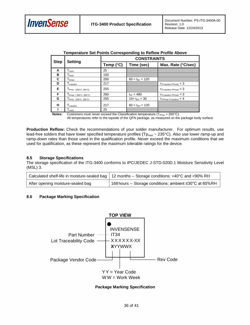
8.6 Package Marking Specification
IT34
X X X X X X-XX
XYYWWX
Lot Traceability Code
Package Vendor Code Rev Code
Y Y = Year Code
W W = Work Week
TOP VIEW
Part Number
INVENSENSE
Package Marking Specification

ITG-3400 Product Specification Document Number: PS-ITG-3400A-00 Revision: 1.0 Release Date: 12/24/2013
37 of 41
8.7 Tape & Reel Specification
Tape Dimensions
Reel Outline Drawing
Reel Dimensions and Package Size
PACKAGE
SIZE
REEL (mm)
L V W Z
3x3 330 102 12.8 2.3
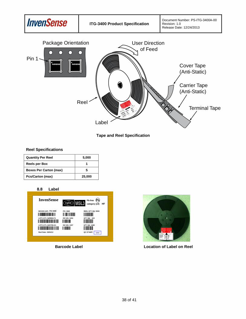
ITG-3400 Product Specification Document Number: PS-ITG-3400A-00 Revision: 1.0 Release Date: 12/24/2013
38 of 41
Tape and Reel Specification
Reel Specifications
Quantity Per Reel 5,000
Reels per Box 1
Boxes Per Carton (max) 5
Pcs/Carton (max) 25,000
8.8 Label
Barcode Label Location of Label on Reel
Label
Reel
Cover Tape
(Anti-Static)
Carrier Tape
(Anti-Static)
Terminal Tape
User Direction
of Feed
INVENSENSE INVENSENSEINVENSENSE INVENSENSE
Pin 1
Package Orientation
InvenSense
P b -f r e e
ca t e g o r y ( e4 )HF
D E VIC E (1P ): M P U-605 0P O : H UB
RE EL Q T Y (Q ): 500 0
L O T 1 (1 T ): Q 2R784 -F1
D /C(D ): 111 8
Q T Y (Q ): 300 0
L O T 2 (1 T ): Q 3V 215 -G1
D /C(D
): 110 7
Q T Y (Q): 200 0
Ree l D a te : 18 /05 /11
Q C S T AM P :
InvenSense Pb-free
category (e4) HF
DEVICE (1P): MPU-6880 PO: HUB REEL QTY (Q): 5000
LOT1 (1T): Q2R994-F1 D/C (D): 1204 QTY (Q): 615
LOT2 (1T): Q3X785-G1 D/C (D): 1207 QTY (Q): 4385
Reel Date: 28/04/12 QC STAMP:
ITG-3400

ITG-3400 Product Specification Document Number: PS-ITG-3400A-00 Revision: 1.0 Release Date: 12/24/2013
39 of 41
8.9 Packaging
REEL – with Barcode & Vacuum-Sealed Moisture MSL3 Label
Caution labels Barrier Bag with ESD, MSL3,
Caution, and Barcode Labels
Caution Label ESD Label Inner Bubble Wrap
Pizza Box Pizza Boxes Placed in Foam- Outer Shipper Label
Lined Shipper Box
ITG-3400 Product Specification Document Number: PS-ITG-3400A-00 Revision: 1.0 Release Date: 12/24/2013
40 of 41
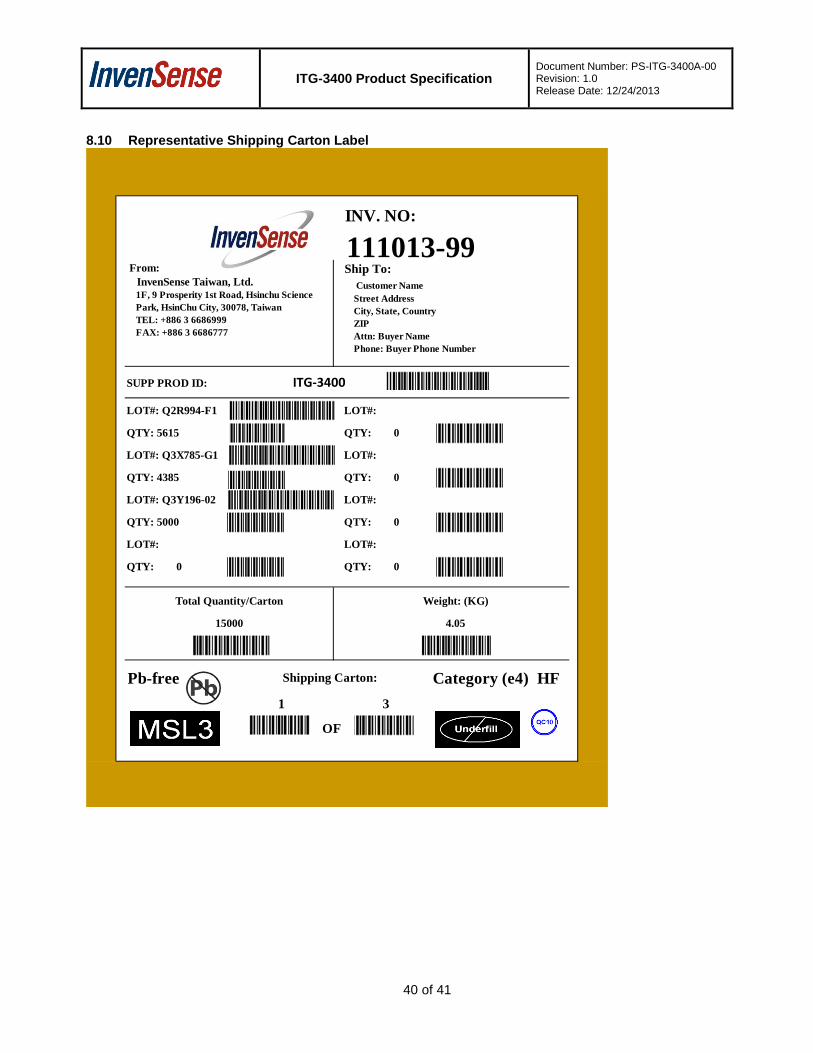
8.10 Representative Shipping Carton Label
INV. NO:
111013-99
SUPP PROD ID: MPU-6880
QTY: 5615 QTY: 0
QTY: 4385 QTY: 0
QTY: 5000 QTY: 0
QTY: 0 QTY: 0
Pb-free Category (e4) HF
1 3
15000 4.05
Shipping Carton:
OF
LOT#: Q3Y196-02 LOT#:
LOT#: LOT#:
Total Quantity/Carton Weight: (KG)
From:
InvenSense Taiwan, Ltd.
1F, 9 Prosperity 1st Road, Hsinchu Science
Park, HsinChu City, 30078, Taiwan
TEL: +886 3 6686999
FAX: +886 3 6686777
Ship To:
Customer Name
Street Address
City, State, Country
ZIP
Attn: Buyer Name
Phone: Buyer Phone Number
LOT#: Q2R994-F1 LOT#:
LOT#: Q3X785-G1 LOT#:
ITG-3400
ITG-3400 Product Specification Document Number: PS-ITG-3400A-00 Revision: 1.0 Release Date: 12/24/2013
41 of 41
9 Environmental Compliance The ITG-3400 is RoHS and Green compliant.
The ITG-3400 is in full environmental compliance as evidenced in report HS-ITG-3400A, Materials Declaration Data Sheet.
Environmental Declaration Disclaimer:
InvenSense believes this environmental information to be correct but cannot guarantee accuracy or completeness. Conformity documents for the above component constitutes are on file. InvenSense subcontracts manufacturing and the information contained herein is based on data received from vendors and suppliers, which has not been validated by InvenSense.
This information furnished by InvenSense is believed to be accurate and reliable. However, no responsibility is assumed by InvenSense for its use, or for any infringements of patents or other rights of third parties that may result from its use. Specifications are subject to change without notice. InvenSense reserves the right to make changes to this product, including its circuits and software, in order to improve its design and/or performance, without prior notice. InvenSense makes no warranties, neither expressed nor implied, regarding the information and specifications contained in this document. InvenSense assumes no responsibility for any claims or damages arising from information contained in this document, or from the use of products and services detailed therein. This includes, but is not limited to, claims or damages based on the infringement of patents, copyrights, mask work and/or other intellectual property rights.
Certain intellectual property owned by InvenSense and described in this document is patent protected. No license is granted by implication or otherwise under any patent or patent rights of InvenSense. This publication supersedes and replaces all information previously supplied. Trademarks that are registered trademarks are the property of their respective companies. InvenSense sensors should not be used or sold in the development, storage, production or utilization of any conventional or mass-destructive weapons or for any other weapons or life threatening applications, as well as in any other life critical applications such as medical equipment, transportation, aerospace and nuclear instruments, undersea equipment, power plant equipment, disaster prevention and crime prevention equipment.
©2013 InvenSense, Inc. All rights reserved. InvenSense, MotionTracking, MotionProcessing, MotionProcessor, MotionFusion, MotionApps, DMP, and the InvenSense logo are trademarks of InvenSense, Inc. Other company and product names may be trademarks of the respective companies with which they are associated.
©2013 InvenSense, Inc. All rights reserved.
InvenSense Inc.
1745 Technology Drive, San Jose, CA 95110 U.S.A. Tel: +1 (408) 988-7339 Fax: +1 (408) 988-8104
Website: www.invensense.com
Document Number: RM-000002 Revision: 1.0 Release Date: 08/04/2014
ITG-3400 Register Map and Descriptions
Revision 1.0
CONFIDENTIAL & PROPRIETARY 1 of 20
ITG-3400 Register Map and Descriptions Document Number: RM-000002 Revision: 1.0 Release Date: 08/04/2014
CONTENTS 1 REVISION HISTORY ................................................................................................................................... 3
2 PURPOSE AND SCOPE ............................................................................................................................. 4
3 REGISTER MAP .......................................................................................................................................... 5
4 REGISTER DESCRIPTIONS ....................................................................................................................... 7
4.1 REGISTERS 0 TO 2 – GYROSCOPE SELF-TEST REGISTERS .................................................................... 7
4.2 REGISTERS 19 TO 24 – GYRO OFFSET REGISTERS ............................................................................... 8 4.3 REGISTER 25 – SAMPLE RATE DIVIDER ................................................................................................ 9
4.4 REGISTER 26 – CONFIGURATION .......................................................................................................... 9
4.5 REGISTER 27 – GYROSCOPE CONFIGURATION .................................................................................... 10
4.6 REGISTER 35 – FIFO ENABLE ............................................................................................................ 11
4.7 REGISTER 55 – INT PIN ENABLE CONFIGURATION............................................................................... 12
4.8 REGISTER 56 – INTERRUPT ENABLE ................................................................................................... 12 4.9 REGISTER 58 – INTERRUPT STATUS ................................................................................................... 13
4.10 REGISTERS 65 AND 66 – TEMPERATURE MEASUREMENT ..................................................................... 14
4.11 REGISTERS 67 TO 72 – GYROSCOPE MEASUREMENTS ........................................................................ 14
4.12 REGISTER 104 – SIGNAL PATH RESET ................................................................................................ 16
4.13 REGISTER 106 – USER CONTROL ....................................................................................................... 16
4.14 REGISTER 107 – POWER MANAGEMENT 1 .......................................................................................... 17 4.15 REGISTER 114 AND 115 – FIFO COUNT REGISTERS ........................................................................... 18
4.16 REGISTER 116 – FIFO READ WRITE .................................................................................................. 18
4.17 REGISTER 117 – WHO AM I ................................................................................................................ 19
CONFIDENTIAL & PROPRIETARY 2 of 20
ITG-3400 Register Map and Descriptions Document Number: RM-000002 Revision: 1.0 Release Date: 08/04/2014
1 Revision History
Revision Date Revision Description 08/04/2014 1.0 Initial Release
CONFIDENTIAL & PROPRIETARY 3 of 20

ITG-3400 Register Map and Descriptions Document Number: RM-000002 Revision: 1.0 Release Date: 08/04/2014
2 Purpose and Scope This document provides preliminary information regarding the register map and descriptions for 3-axis gyroscope ITG-3400. This document should be used in conjunction with the ITG-3400 Product Specification (PS-ITG-3400A-00) for detailed features, specifications, and other product information.
CONFIDENTIAL & PROPRIETARY 4 of 20
ITG-3400 Register Map and Descriptions Document Number: RM-000002 Revision: 1.0 Release Date: 08/04/2014
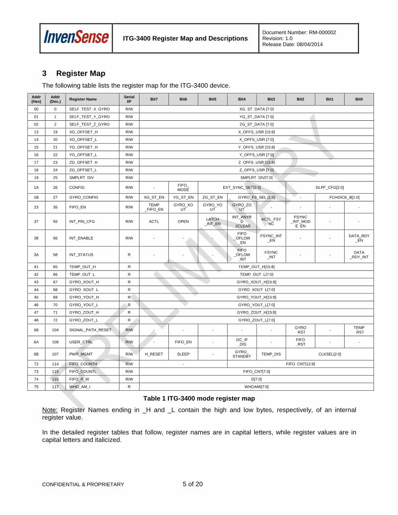
3 Register Map The following table lists the register map for the ITG-3400 device.
Addr (Hex)
Addr (Dec.) Register Name Serial
I/F Bit7 Bit6 Bit5 Bit4 Bit3 Bit2 Bit1 Bit0
00 0 SELF_TEST_X_GYRO R/W XG_ST_DATA [7:0]
01 1 SELF_TEST_Y_GYRO R/W YG_ST_DATA [7:0]
02 2 SELF_TEST_Z_GYRO R/W ZG_ST_DATA [7:0]
13 19 XG_OFFSET_H R/W X_OFFS_USR [15:8]
14 20 XG_OFFSET_L R/W X_OFFS_USR [7:0]
15 21 YG_OFFSET_H R/W Y_OFFS_USR [15:8]
16 22 YG_OFFSET_L R/W Y_OFFS_USR [7:0]
17 23 ZG_OFFSET_H R/W Z_OFFS_USR [15:8]
18 24 ZG_OFFSET_L R/W Z_OFFS_USR [7:0]
19 25 SMPLRT_DIV R/W SMPLRT_DIV[7:0]
1A 26 CONFIG R/W - FIFO_ MODE EXT_SYNC_SET[2:0] DLPF_CFG[2:0]
1B 27 GYRO_CONFIG R/W XG_ST_EN YG_ST_EN ZG_ST_EN GYRO_FS_SEL [1:0] - FCHOICE_B[1:0]
23 35 FIFO_EN R/W TEMP _FIFO_EN
GYRO_XOUT
GYRO_YOUT
GYRO_ZOUT - - - -
37 55 INT_PIN_CFG R/W ACTL OPEN LATCH _INT_EN
INT_ANYRD
_2CLEAR
ACTL_FSYNC
FSYNC _INT_MOD
E_EN - -
38 56 INT_ENABLE R/W - - - FIFO
_OFLOW _EN
FSYNC_INT_EN - - DATA_RDY
_EN
3A 58 INT_STATUS R - - - FIFO
_OFLOW _INT
FSYNC _INT - - DATA
_RDY_INT
41 65 TEMP_OUT_H R TEMP_OUT_H[15:8]
42 66 TEMP_OUT_L R TEMP_OUT_L[7:0]
43 67 GYRO_XOUT_H R GYRO_XOUT_H[15:8]
44 68 GYRO_XOUT_L R GYRO_XOUT_L[7:0]
45 69 GYRO_YOUT_H R GYRO_YOUT_H[15:8]
46 70 GYRO_YOUT_L R GYRO_YOUT_L[7:0]
47 71 GYRO_ZOUT_H R GYRO_ZOUT_H[15:8]
48 72 GYRO_ZOUT_L R GYRO_ZOUT_L[7:0]
68 104 SIGNAL_PATH_RESET R/W - - - - - GYRO _RST - TEMP
_RST
6A 106 USER_CTRL R/W - FIFO_EN - I2C_IF _DIS - FIFO
_RST - -
6B 107 PWR_MGMT R/W H_RESET SLEEP - GYRO_ STANDBY TEMP_DIS CLKSEL[2:0]
72 114 FIFO_COUNTH R/W - FIFO_CNT[12:8]
73 115 FIFO_COUNTL R/W FIFO_CNT[7:0]
74 116 FIFO_R_W R/W D[7:0]
75 117 WHO_AM_I R WHOAMI[7:0]
Table 1 ITG-3400 mode register map
Note: Register Names ending in _H and _L contain the high and low bytes, respectively, of an internal register value. In the detailed register tables that follow, register names are in capital letters, while register values are in capital letters and italicized.
CONFIDENTIAL & PROPRIETARY 5 of 20

ITG-3400 Register Map and Descriptions Document Number: RM-000002 Revision: 1.0 Release Date: 08/04/2014
The reset value is 0x00 for all registers other than the registers below, also the self-test registers contain pre-programmed values and will not be 0x00 after reset.
• Register 107 (0x01) Power Management 1 • Register 117 (0x78) WHO_AM_I
CONFIDENTIAL & PROPRIETARY 6 of 20
ITG-3400 Register Map and Descriptions Document Number: RM-000002 Revision: 1.0 Release Date: 08/04/2014
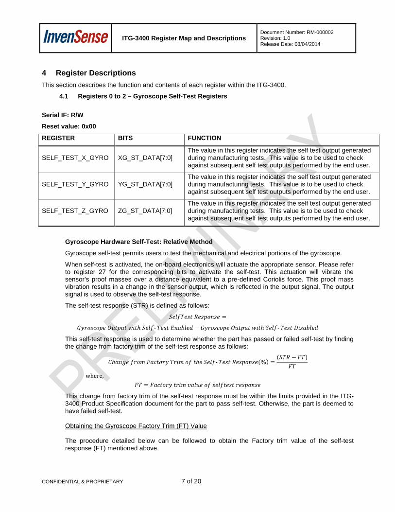
4 Register Descriptions This section describes the function and contents of each register within the ITG-3400.
4.1 Registers 0 to 2 – Gyroscope Self-Test Registers
Serial IF: R/W
Reset value: 0x00
REGISTER BITS FUNCTION
SELF_TEST_X_GYRO XG_ST_DATA[7:0] The value in this register indicates the self test output generated during manufacturing tests. This value is to be used to check against subsequent self test outputs performed by the end user.
SELF_TEST_Y_GYRO YG_ST_DATA[7:0] The value in this register indicates the self test output generated during manufacturing tests. This value is to be used to check against subsequent self test outputs performed by the end user.
SELF_TEST_Z_GYRO ZG_ST_DATA[7:0] The value in this register indicates the self test output generated during manufacturing tests. This value is to be used to check against subsequent self test outputs performed by the end user.
Gyroscope Hardware Self-Test: Relative Method
Gyroscope self-test permits users to test the mechanical and electrical portions of the gyroscope.
When self-test is activated, the on-board electronics will actuate the appropriate sensor. Please refer to register 27 for the corresponding bits to activate the self-test. This actuation will vibrate the sensor’s proof masses over a distance equivalent to a pre-defined Coriolis force. This proof mass vibration results in a change in the sensor output, which is reflected in the output signal. The output signal is used to observe the self-test response.
The self-test response (STR) is defined as follows:
𝑆𝑒𝑙𝑓𝑇𝑒𝑠𝑡 𝑅𝑒𝑠𝑝𝑜𝑛𝑠𝑒 =
𝐺𝑦𝑟𝑜𝑠𝑐𝑜𝑝𝑒 𝑂𝑢𝑡𝑝𝑢𝑡 𝑤𝑖𝑡ℎ 𝑆𝑒𝑙𝑓-𝑇𝑒𝑠𝑡 𝐸𝑛𝑎𝑏𝑙𝑒𝑑 − 𝐺𝑦𝑟𝑜𝑠𝑐𝑜𝑝𝑒 𝑂𝑢𝑡𝑝𝑢𝑡 𝑤𝑖𝑡ℎ 𝑆𝑒𝑙𝑓-𝑇𝑒𝑠𝑡 𝐷𝑖𝑠𝑎𝑏𝑙𝑒𝑑
This self-test response is used to determine whether the part has passed or failed self-test by finding the change from factory trim of the self-test response as follows:
𝐶ℎ𝑎𝑛𝑔𝑒 𝑓𝑟𝑜𝑚 𝐹𝑎𝑐𝑡𝑜𝑟𝑦 𝑇𝑟𝑖𝑚 𝑜𝑓 𝑡ℎ𝑒 𝑆𝑒𝑙𝑓-𝑇𝑒𝑠𝑡 𝑅𝑒𝑠𝑝𝑜𝑛𝑠𝑒(%) =(𝑆𝑇𝑅 − 𝐹𝑇)
𝐹𝑇
where, 𝐹𝑇 = 𝐹𝑎𝑐𝑡𝑜𝑟𝑦 𝑡𝑟𝑖𝑚 𝑣𝑎𝑙𝑢𝑒 𝑜𝑓 𝑠𝑒𝑙𝑓𝑡𝑒𝑠𝑡 𝑟𝑒𝑠𝑝𝑜𝑛𝑠𝑒
This change from factory trim of the self-test response must be within the limits provided in the ITG-3400 Product Specification document for the part to pass self-test. Otherwise, the part is deemed to have failed self-test.
Obtaining the Gyroscope Factory Trim (FT) Value The procedure detailed below can be followed to obtain the Factory trim value of the self-test response (FT) mentioned above.
CONFIDENTIAL & PROPRIETARY 7 of 20
ITG-3400 Register Map and Descriptions Document Number: RM-000002 Revision: 1.0 Release Date: 08/04/2014
The Factory trim value of the self-test response (FT) is calculated as shown below. FT[Xg], FT[Yg], and FT[Zg] refer to the factory trim (FT) values for the gyroscope X, Y, and Z axes, respectively. XG_TEST is the decimal version of XG_ST_DATA[7-0], YG_TEST is the decimal version of YG_ST_DATA[7-0], and ZG_TEST is the decimal version of ZG_ST_DATA[7-0].
When performing self-test for the gyroscope, the full-scale range should be set to ±250dps.
FT [Xg] = 20 ∗ 1.01(𝑋𝐺_𝑇𝐸𝑆𝑇−1) if XG_TEST ≠ 0 FT [Yg] = 20 ∗ 1.01(𝑌𝐺_𝑇𝐸𝑆𝑇−1) if YG_TEST ≠ 0 FT [Zg] = 20 ∗ 1.01(𝑍𝐺_𝑇𝐸𝑆𝑇−1) if ZG_TEST ≠ 0
If XG_TEST, YG_TEST, or ZG_TEST is 0, it indicates no FT data. Relative method does not apply in this case.
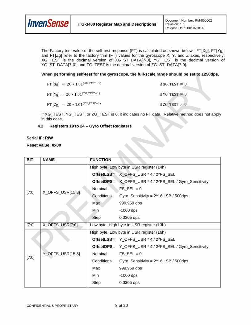
4.2 Registers 19 to 24 – Gyro Offset Registers
Serial IF: R/W
Reset value: 0x00
BIT NAME FUNCTION
[7:0] X_OFFS_USR[15:8]
High byte, Low byte in USR register (14h) OffsetLSB= X_OFFS_USR * 4 / 2^FS_SEL
OffsetDPS= X_OFFS_USR * 4 / 2^FS_SEL / Gyro_Sensitivity Nominal Conditions
FS_SEL = 0 Gyro_Sensitivity = 2^16 LSB / 500dps
Max 999.969 dps Min -1000 dps Step 0.0305 dps
[7:0] X_OFFS_USR[7:0] Low byte, High byte in USR register (13h)
[7:0] Y_OFFS_USR[15:8]
High byte, Low byte in USR register (16h) OffsetLSB= Y_OFFS_USR * 4 / 2^FS_SEL
OffsetDPS= Y_OFFS_USR * 4 / 2^FS_SEL / Gyro_Sensitivity Nominal Conditions
FS_SEL = 0 Gyro_Sensitivity = 2^16 LSB / 500dps
Max 999.969 dps Min -1000 dps Step 0.0305 dps
CONFIDENTIAL & PROPRIETARY 8 of 20
ITG-3400 Register Map and Descriptions Document Number: RM-000002 Revision: 1.0 Release Date: 08/04/2014
BIT NAME FUNCTION
[7:0] Y_OFFS_USR[7:0] Low byte, High byte in USR register (15h)
[7:0] Z_OFFS_USR[15:8]
High byte, Low byte in USR register (18h) OffsetLSB= Z_OFFS_USR * 4 / 2^FS_SEL
OffsetDPS= Z_OFFS_USR * 4 / 2^FS_SEL / Gyro_Sensitivity Nominal Conditions
FS_SEL = 0 Gyro_Sensitivity = 2^16 LSB / 500dps
Max 999.969 dps Min -1000 dps Step 0.0305 dps
[7:0] Z_OFFS_USR[7:0] Low byte, High byte in USR register (17h)
These registers are used to remove DC bias from the gyro sensor data output for X, Y and Z axes. The values in these registers are subtracted from the gyro sensor values before going into the sensor registers. Please refer to registers 67 to 72 for units.
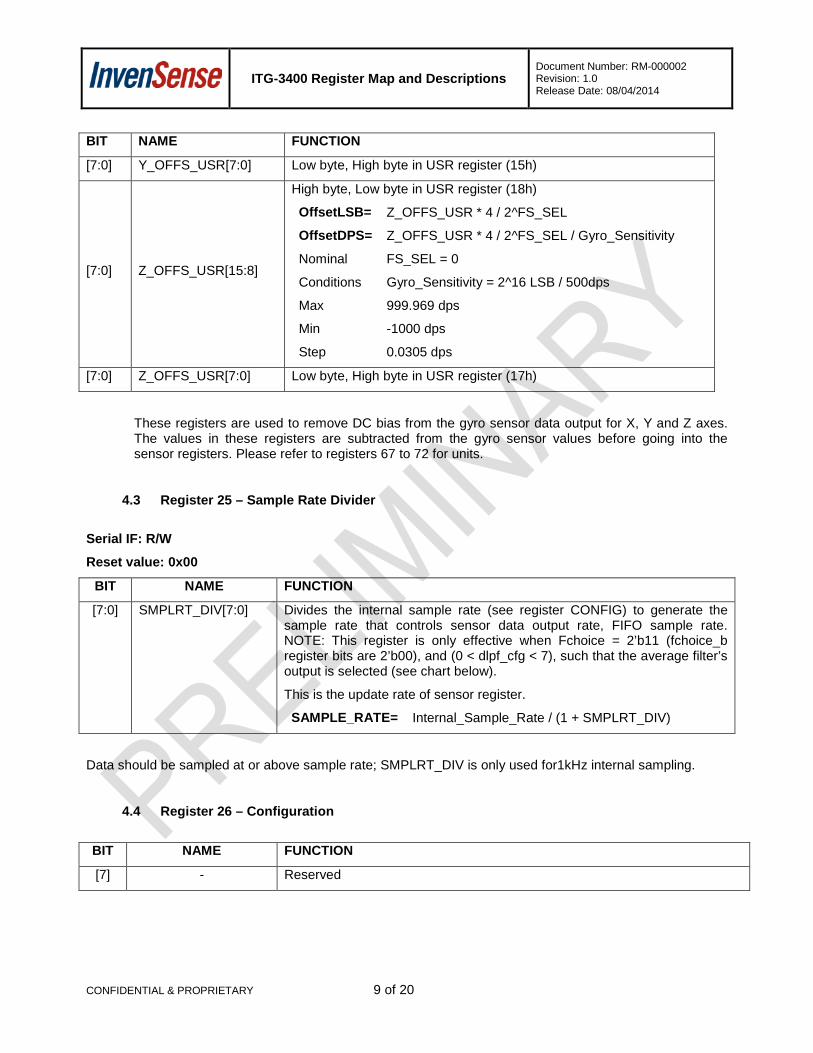
4.3 Register 25 – Sample Rate Divider
Serial IF: R/W
Reset value: 0x00
BIT NAME FUNCTION
[7:0] SMPLRT_DIV[7:0] Divides the internal sample rate (see register CONFIG) to generate the sample rate that controls sensor data output rate, FIFO sample rate. NOTE: This register is only effective when Fchoice = 2’b11 (fchoice_b register bits are 2’b00), and (0 < dlpf_cfg < 7), such that the average filter’s output is selected (see chart below).
This is the update rate of sensor register.
SAMPLE_RATE= Internal_Sample_Rate / (1 + SMPLRT_DIV)
Data should be sampled at or above sample rate; SMPLRT_DIV is only used for1kHz internal sampling.
4.4 Register 26 – Configuration
BIT NAME FUNCTION
[7] - Reserved
CONFIDENTIAL & PROPRIETARY 9 of 20
ITG-3400 Register Map and Descriptions Document Number: RM-000002 Revision: 1.0 Release Date: 08/04/2014
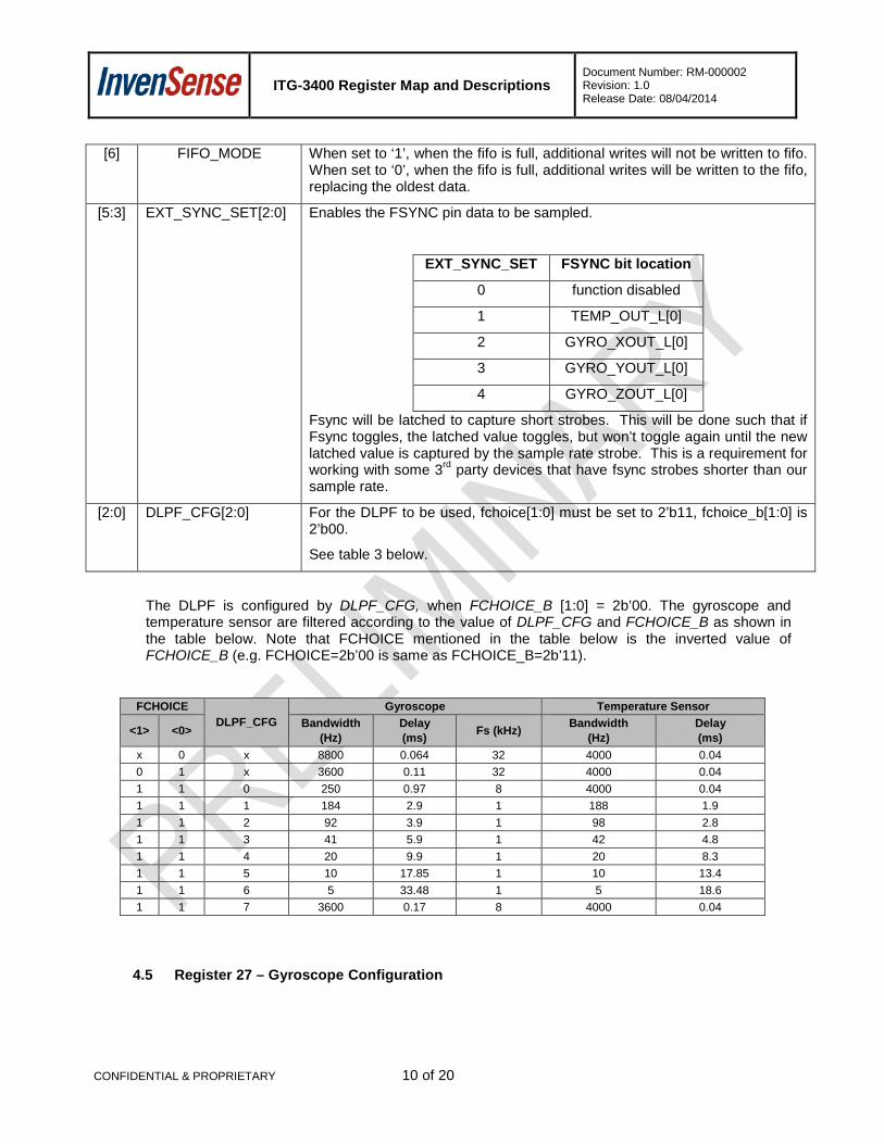
[6] FIFO_MODE When set to ‘1’, when the fifo is full, additional writes will not be written to fifo. When set to ‘0’, when the fifo is full, additional writes will be written to the fifo, replacing the oldest data.
[5:3] EXT_SYNC_SET[2:0] Enables the FSYNC pin data to be sampled.
EXT_SYNC_SET FSYNC bit location
0 function disabled 1 TEMP_OUT_L[0] 2 GYRO_XOUT_L[0] 3 GYRO_YOUT_L[0] 4 GYRO_ZOUT_L[0]
Fsync will be latched to capture short strobes. This will be done such that if Fsync toggles, the latched value toggles, but won’t toggle again until the new latched value is captured by the sample rate strobe. This is a requirement for working with some 3rd party devices that have fsync strobes shorter than our sample rate.
[2:0] DLPF_CFG[2:0] For the DLPF to be used, fchoice[1:0] must be set to 2’b11, fchoice_b[1:0] is 2’b00.
See table 3 below.
The DLPF is configured by DLPF_CFG, when FCHOICE_B [1:0] = 2b’00. The gyroscope and temperature sensor are filtered according to the value of DLPF_CFG and FCHOICE_B as shown in the table below. Note that FCHOICE mentioned in the table below is the inverted value of FCHOICE_B (e.g. FCHOICE=2b’00 is same as FCHOICE_B=2b’11).
FCHOICE DLPF_CFG
Gyroscope Temperature Sensor
<1> <0> Bandwidth (Hz)
Delay (ms) Fs (kHz) Bandwidth
(Hz) Delay (ms)
x 0 x 8800 0.064 32 4000 0.04 0 1 x 3600 0.11 32 4000 0.04 1 1 0 250 0.97 8 4000 0.04 1 1 1 184 2.9 1 188 1.9 1 1 2 92 3.9 1 98 2.8 1 1 3 41 5.9 1 42 4.8 1 1 4 20 9.9 1 20 8.3 1 1 5 10 17.85 1 10 13.4 1 1 6 5 33.48 1 5 18.6 1 1 7 3600 0.17 8 4000 0.04
4.5 Register 27 – Gyroscope Configuration
CONFIDENTIAL & PROPRIETARY 10 of 20

ITG-3400 Register Map and Descriptions Document Number: RM-000002 Revision: 1.0 Release Date: 08/04/2014
Serial IF: R/W
Reset value: 0x00
BIT NAME FUNCTION
[7] XG_ST_EN X Gyro self-test [6] YG_ST_EN Y Gyro self-test [5] ZG_ST_EN Z Gyro self-test
[4:3] GYRO_FS_SEL[1:0]
Gyro Full Scale Select: 00 = ±250dps 01= ±500dps 10 = ±1000dps 11 = ±2000dps
[2] - Reserved
[1:0] FCHOICE_B[1:0] Used to bypass DLPF as shown in table 1 above. NOTE: Register is FCHOICE_B (inverted version of FCHOICE), table 1 uses FCHOICE (which is the inverted version of this register).
4.6 Register 35 – FIFO Enable
Serial IF: R/W
Reset value: 0x00
BIT NAME FUNCTION
[7] TEMP_OUT 1 – Write TEMP_OUT_H and TEMP_OUT_L to the FIFO at the sample rate; If enabled, buffering of data occurs even if data path is in standby. 0 – function is disabled
[6] GYRO_XOUT 1 – Write GYRO_XOUT_H and GYRO_XOUT_L to the FIFO at the sample rate; If enabled, buffering of data occurs even if data path is in standby. 0 – function is disabled
[5] GYRO_YOUT
1 – Write GYRO_YOUT_H and GYRO_YOUT_L to the FIFO at the sample rate; If enabled, buffering of data occurs even if data path is in standby. 0 – function is disabled NOTE: Enabling any one of the bits corresponding to the Gyros or Temp data paths, data is buffered into the FIFO even though that data path is not enabled.
[4] GYRO_ZOUT 1 – Write GYRO_ZOUT_H and GYRO_ZOUT_L to the FIFO at the sample rate; If enabled, buffering of data occurs even if data path is in standby. 0 – function is disabled
CONFIDENTIAL & PROPRIETARY 11 of 20
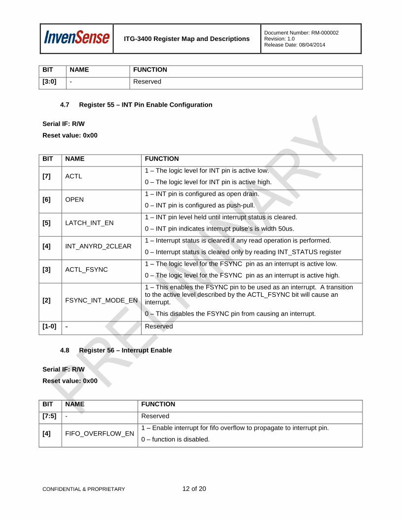
ITG-3400 Register Map and Descriptions Document Number: RM-000002 Revision: 1.0 Release Date: 08/04/2014
BIT NAME FUNCTION
[3:0] - Reserved
4.7 Register 55 – INT Pin Enable Configuration
Serial IF: R/W
Reset value: 0x00
BIT NAME FUNCTION
[7] ACTL 1 – The logic level for INT pin is active low. 0 – The logic level for INT pin is active high.
[6] OPEN 1 – INT pin is configured as open drain. 0 – INT pin is configured as push-pull.
[5] LATCH_INT_EN 1 – INT pin level held until interrupt status is cleared. 0 – INT pin indicates interrupt pulse’s is width 50us.
[4] INT_ANYRD_2CLEAR 1 – Interrupt status is cleared if any read operation is performed. 0 – Interrupt status is cleared only by reading INT_STATUS register
[3] ACTL_FSYNC 1 – The logic level for the FSYNC pin as an interrupt is active low. 0 – The logic level for the FSYNC pin as an interrupt is active high.
[2] FSYNC_INT_MODE_EN
1 – This enables the FSYNC pin to be used as an interrupt. A transition to the active level described by the ACTL_FSYNC bit will cause an interrupt. 0 – This disables the FSYNC pin from causing an interrupt.
[1-0] - Reserved
4.8 Register 56 – Interrupt Enable
Serial IF: R/W
Reset value: 0x00
BIT NAME FUNCTION
[7:5] - Reserved
[4] FIFO_OVERFLOW_EN 1 – Enable interrupt for fifo overflow to propagate to interrupt pin. 0 – function is disabled.
CONFIDENTIAL & PROPRIETARY 12 of 20
ITG-3400 Register Map and Descriptions Document Number: RM-000002 Revision: 1.0 Release Date: 08/04/2014
BIT NAME FUNCTION
[3] FSYNC_INT_EN 1 – Enable Fsync interrupt to propagate to interrupt pin. 0 – function is disabled.
[2:1] - Reserved
[0] DATA_RDY_EN 1 – Enable Raw Sensor Data Ready interrupt to propagate to interrupt pin.
0 – function is disabled.
4.9 Register 58 – Interrupt Status
Serial IF: R/C
Reset value: 0x00
BIT NAME FUNCTION
[7:5] - Reserved
[4] FIFO_OVERFLOW_INT 1 – Fifo Overflow interrupt occurred. Note that the oldest data is has been dropped from the fifo.
[3] FSYNC_INT 1 – Fsync interrupt occurred.
[2:1] - Reserved
[0] DATA_RDY_INT This bit automatically sets to 1 when a Data Ready interrupt is generated. The bit clears to 0 after the register has been read.
CONFIDENTIAL & PROPRIETARY 13 of 20
ITG-3400 Register Map and Descriptions Document Number: RM-000002 Revision: 1.0 Release Date: 08/04/2014
4.10 Registers 65 and 66 – Temperature Measurement
Name: TEMP_OUT_H
Serial IF: R
Reset value: 0x00 (if sensor disabled)
BIT NAME FUNCTION
[7:0] TEMP_OUT_H[15:8] High byte of the temperature sensor output
Name: TEMP_OUT_L
Serial IF: R
Reset value: 0x00 (if sensor disabled)
BIT NAME FUNCTION
[7:0] TEMP_OUT_L[7:0]
Low byte of the temperature sensor output TEMP_degC = ((TEMP_OUT –
RoomTemp_Offset)/Temp_Sensitivity) + 25degC
4.11 Registers 67 to 72 – Gyroscope Measurements Name: GYRO_XOUT_H
Serial IF: R
Reset value: 0x00 (if sensor disabled)
BIT NAME FUNCTION
[7:0] GYRO_XOUT_H[7:0] High byte of the X-Axis gyroscope output
Name: GYRO_XOUT_L
Serial IF: R
Reset value: 0x00 (if sensor disabled)
BIT NAME FUNCTION
CONFIDENTIAL & PROPRIETARY 14 of 20
ITG-3400 Register Map and Descriptions Document Number: RM-000002 Revision: 1.0 Release Date: 08/04/2014
BIT NAME FUNCTION
[7:0] GYRO_XOUT_L[7:0]
Low byte of the X-Axis gyroscope output GYRO_XOUT = Gyro_Sensitivity * X_angular_rate
Nominal
Conditions
FS_SEL = 0 Gyro_Sensitivity = 131 LSB/(º/s)
Name: GYRO_YOUT_H
Serial IF: R
Reset value: 0x00 (if sensor disabled)
BIT NAME FUNCTION
[7:0] GYRO_YOUT_H[7:0] High byte of the Y-Axis gyroscope output
Name: GYRO_YOUT_L
Serial IF: R
Reset value: 0x00 (if sensor disabled)
BIT NAME FUNCTION
[7:0] GYRO_YOUT_L[7:0]
Low byte of the Y-Axis gyroscope output
GYRO_YOUT = Gyro_Sensitivity * Y_angular_rate
Nominal
Conditions
FS_SEL = 0 Gyro_Sensitivity = 131 LSB/(º/s)
Name: GYRO_ZOUT_H
Serial IF: R
Reset value: 0x00 (if sensor disabled)
BIT NAME FUNCTION
[7:0] GYRO_ZOUT_H[7:0] High byte of the Z-Axis gyroscope output
Name: GYRO_ZOUT_L
Serial IF: R
Reset value: 0x00 (if sensor disabled)
CONFIDENTIAL & PROPRIETARY 15 of 20
ITG-3400 Register Map and Descriptions Document Number: RM-000002 Revision: 1.0 Release Date: 08/04/2014
BIT NAME FUNCTION
[7:0] GYRO_ZOUT_L[7:0]
Low byte of the Z-Axis gyroscope output GYRO_ZOUT = Gyro_Sensitivity * Z_angular_rate
Nominal
Conditions
FS_SEL = 0 Gyro_Sensitivity = 131 LSB/(º/s)
4.12 Register 104 – Signal Path Reset SIGNAL_PATH_RESET
Serial IF: R/W
Reset value: 0x00
BIT NAME FUNCTION
[7:3] - Reserved
[2] GYRO_RST Reset gyro digital signal path. Note: Sensor registers are not cleared. Use SIG_COND_RST to clear sensor registers.
[1] - Reserved
[0] TEMP_RST Reset temp digital signal path. Note: Sensor registers are not cleared. Use SIG_COND_RST to clear sensor registers.
4.13 Register 106 – User Control
Name: USER_CTRL
Serial IF: R/W
Reset value: 0x00
BIT NAME FUNCTION
[7] - Reserved
[6] FIFO_EN 1 – Enable FIFO operation mode. 0 – Disable FIFO access from serial interface. To disable FIFO writes by dma, use FIFO_EN register.
[5] - Reserved
[4] I2C_IF_DIS 1 – Reset I2C Slave module and put the serial interface in SPI mode only. This bit auto clears after one clock cycle of the internal 20MHz clock.
[3] - Reserved
CONFIDENTIAL & PROPRIETARY 16 of 20
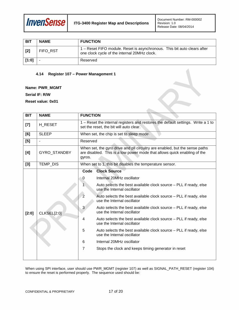
ITG-3400 Register Map and Descriptions Document Number: RM-000002 Revision: 1.0 Release Date: 08/04/2014
BIT NAME FUNCTION
[2] FIFO_RST 1 – Reset FIFO module. Reset is asynchronous. This bit auto clears after one clock cycle of the internal 20MHz clock.
[1:0] - Reserved
4.14 Register 107 – Power Management 1
Name: PWR_MGMT
Serial IF: R/W
Reset value: 0x01
BIT NAME FUNCTION
[7] H_RESET 1 – Reset the internal registers and restores the default settings. Write a 1 to set the reset, the bit will auto clear.
[6] SLEEP When set, the chip is set to sleep mode. [5] - Reserved
[4] GYRO_STANDBY When set, the gyro drive and pll circuitry are enabled, but the sense paths are disabled. This is a low power mode that allows quick enabling of the gyros.
[3] TEMP_DIS When set to 1, this bit disables the temperature sensor.
[2:0] CLKSEL[2:0]
Code Clock Source
0 Internal 20MHz oscillator 1 Auto selects the best available clock source – PLL if ready, else
use the Internal oscillator 2 Auto selects the best available clock source – PLL if ready, else
use the Internal oscillator 3 Auto selects the best available clock source – PLL if ready, else
use the Internal oscillator 4 Auto selects the best available clock source – PLL if ready, else
use the Internal oscillator 5 Auto selects the best available clock source – PLL if ready, else
use the Internal oscillator 6 Internal 20MHz oscillator 7 Stops the clock and keeps timing generator in reset
When using SPI interface, user should use PWR_MGMT (register 107) as well as SIGNAL_PATH_RESET (register 104) to ensure the reset is performed properly. The sequence used should be:
CONFIDENTIAL & PROPRIETARY 17 of 20
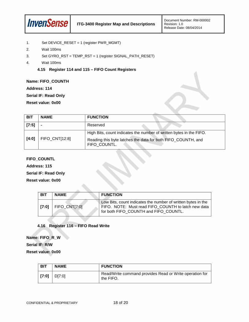
ITG-3400 Register Map and Descriptions Document Number: RM-000002 Revision: 1.0 Release Date: 08/04/2014
1. Set DEVICE_RESET = 1 (register PWR_MGMT)
2. Wait 100ms
3. Set GYRO_RST = TEMP_RST = 1 (register SIGNAL_PATH_RESET)
4. Wait 100ms
4.15 Register 114 and 115 – FIFO Count Registers
Name: FIFO_COUNTH
Address: 114
Serial IF: Read Only
Reset value: 0x00
BIT NAME FUNCTION
[7:5] - Reserved
[4:0] FIFO_CNT[12:8] High Bits, count indicates the number of written bytes in the FIFO. Reading this byte latches the data for both FIFO_COUNTH, and FIFO_COUNTL.
FIFO_COUNTL
Address: 115
Serial IF: Read Only
Reset value: 0x00
BIT NAME FUNCTION
[7:0] FIFO_CNT[7:0] Low Bits, count indicates the number of written bytes in the FIFO. NOTE: Must read FIFO_COUNTH to latch new data for both FIFO_COUNTH and FIFO_COUNTL.
4.16 Register 116 – FIFO Read Write
Name: FIFO_R_W
Serial IF: R/W
Reset value: 0x00
BIT NAME FUNCTION
[7:0] D[7:0] Read/Write command provides Read or Write operation for the FIFO.
CONFIDENTIAL & PROPRIETARY 18 of 20
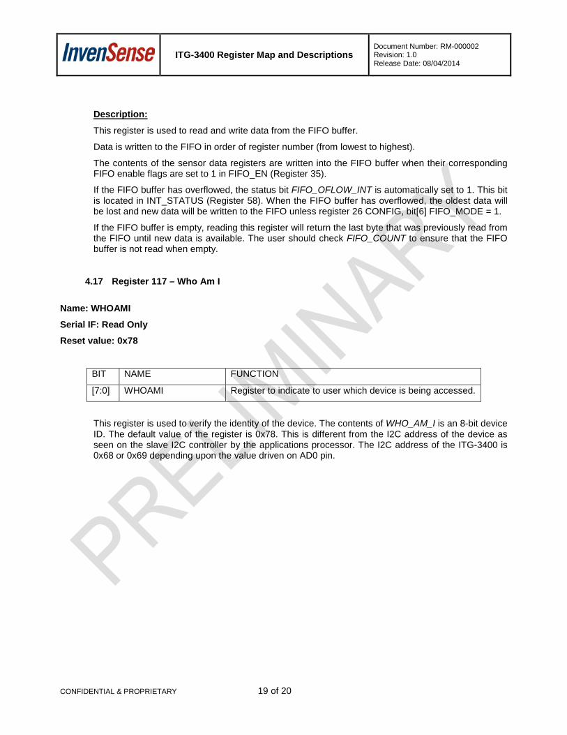
ITG-3400 Register Map and Descriptions Document Number: RM-000002 Revision: 1.0 Release Date: 08/04/2014
Description:
This register is used to read and write data from the FIFO buffer.
Data is written to the FIFO in order of register number (from lowest to highest).
The contents of the sensor data registers are written into the FIFO buffer when their corresponding FIFO enable flags are set to 1 in FIFO_EN (Register 35).
If the FIFO buffer has overflowed, the status bit FIFO_OFLOW_INT is automatically set to 1. This bit is located in INT_STATUS (Register 58). When the FIFO buffer has overflowed, the oldest data will be lost and new data will be written to the FIFO unless register 26 CONFIG, bit[6] FIFO_MODE = 1.
If the FIFO buffer is empty, reading this register will return the last byte that was previously read from the FIFO until new data is available. The user should check FIFO_COUNT to ensure that the FIFO buffer is not read when empty.
4.17 Register 117 – Who Am I
Name: WHOAMI
Serial IF: Read Only
Reset value: 0x78
BIT NAME FUNCTION
[7:0] WHOAMI Register to indicate to user which device is being accessed.
This register is used to verify the identity of the device. The contents of WHO_AM_I is an 8-bit device ID. The default value of the register is 0x78. This is different from the I2C address of the device as seen on the slave I2C controller by the applications processor. The I2C address of the ITG-3400 is 0x68 or 0x69 depending upon the value driven on AD0 pin.
CONFIDENTIAL & PROPRIETARY 19 of 20
ITG-3400 Register Map and Descriptions Document Number: RM-000002 Revision: 1.0 Release Date: 08/04/2014
This information furnished by InvenSense is believed to be accurate and reliable. However, no responsibility is assumed by InvenSense for its use, or for any infringements of patents or other rights of third parties that may result from its use. Specifications are subject to change without notice. InvenSense reserves the right to make changes to this product, including its circuits and software, in order to improve its design and/or performance, without prior notice. InvenSense makes no warranties, neither expressed nor implied, regarding the information and specifications contained in this document. InvenSense assumes no responsibility for any claims or damages arising from information contained in this document, or from the use of products and services detailed therein. This includes, but is not limited to, claims or damages based on the infringement of patents, copyrights, mask work and/or other intellectual property rights.
Certain intellectual property owned by InvenSense and described in this document is patent protected. No license is granted by implication or otherwise under any patent or patent rights of InvenSense. This publication supersedes and replaces all information previously supplied. Trademarks that are registered trademarks are the property of their respective companies. InvenSense sensors should not be used or sold in the development, storage, production or utilization of any conventional or mass-destructive weapons or for any other weapons or life threatening applications, as well as in any other life critical applications such as medical equipment, transportation, aerospace and nuclear instruments, undersea equipment, power plant equipment, disaster prevention and crime prevention equipment.
©2014 InvenSense, Inc. All rights reserved. InvenSense, MotionTracking, MotionProcessing, MotionProcessor, MotionFusion, MotionApps, DMP, AAR, and the InvenSense logo are trademarks of InvenSense, Inc. Other company and product names may be trademarks of the respective companies with which they are associated.
©2014 InvenSense, Inc. All rights reserved.
CONFIDENTIAL & PROPRIETARY 20 of 20