k l university engineering materials hints for assignment ... · pdf filehints for assignment...
TRANSCRIPT
17PH1001
K L UNIVERSITY
ENGINEERING MATERIALS
Hints for Assignment Questions
1. (a) Define Valence band, Conduction band, Fermi Energy level and explain how
solids are classified basing on energy difference between valence and conduction
bands. 7M
There are four types of band structures which are possible at 0 K. The two important energy
bands are:
Valence band: Valence band is the wide range of energies possessed by the valence electrons.
The highest filled energy band where the electrons are present at 0 K. Conduction band:
Conduction band is the wide range of energies possessed by the conduction electrons. A
partially filled or empty energy band where the electrons can increase their energies by going
to higher energy levels within the band when an electric field is applied.
Fermi Energy Level: The highest filled state at 0 K is called Fermi Energy (EF).
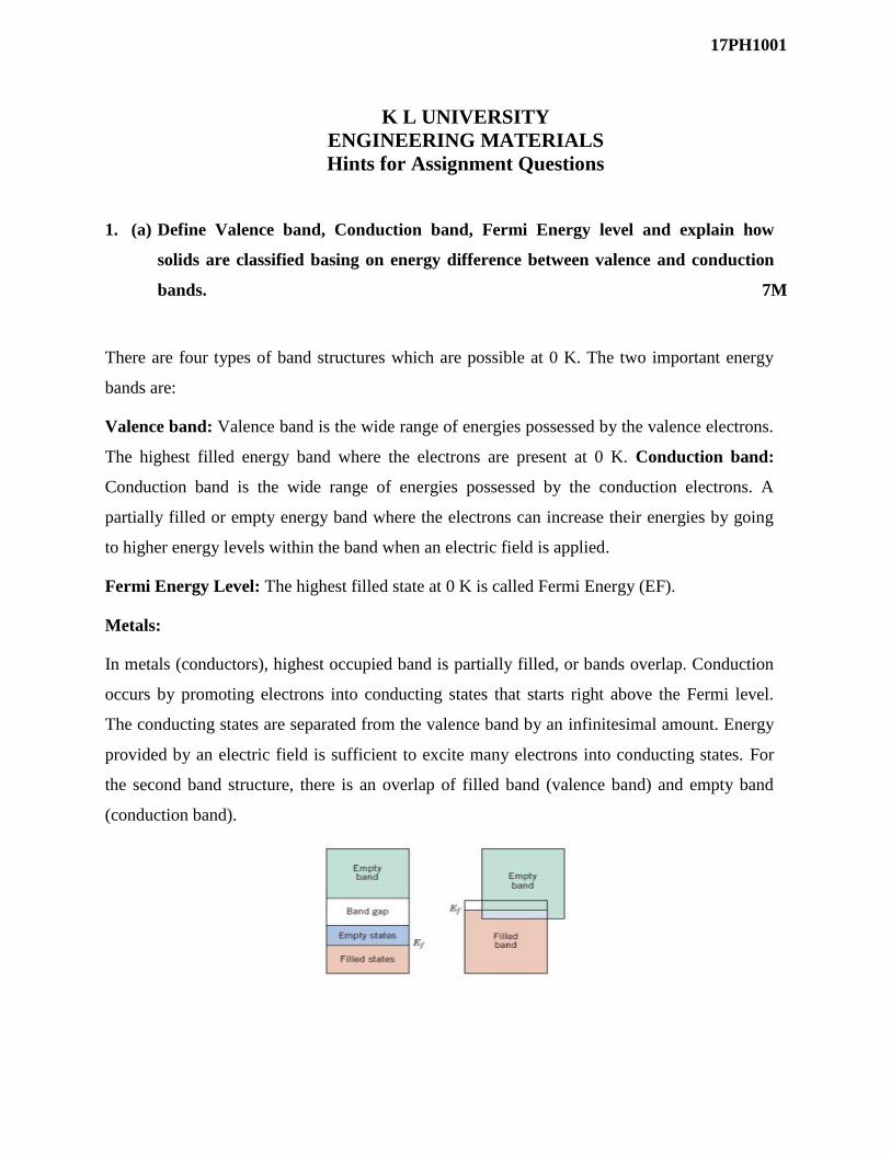
Metals:
In metals (conductors), highest occupied band is partially filled, or bands overlap. Conduction
occurs by promoting electrons into conducting states that starts right above the Fermi level.
The conducting states are separated from the valence band by an infinitesimal amount. Energy
provided by an electric field is sufficient to excite many electrons into conducting states. For
the second band structure, there is an overlap of filled band (valence band) and empty band
(conduction band).
17PH1001
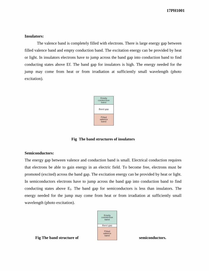
Insulators:
The valence band is completely filled with electrons. There is large energy gap between
filled valence band and empty conduction band. The excitation energy can be provided by heat
or light. In insulators electrons have to jump across the band gap into conduction band to find
conducting states above Ef. The band gap for insulators is high. The energy needed for the
jump may come from heat or from irradiation at sufficiently small wavelength (photo
excitation).
Fig The band structures of insulators
Semiconductors:
The energy gap between valence and conduction band is small. Electrical conduction requires
that electrons be able to gain energy in an electric field. To become free, electrons must be
promoted (excited) across the band gap. The excitation energy can be provided by heat or light.
In semiconductors electrons have to jump across the band gap into conduction band to find
conducting states above Ef. The band gap for semiconductors is less than insulators. The
energy needed for the jump may come from heat or from irradiation at sufficiently small
wavelength (photo excitation).
Fig The band structure of semiconductors.
17PH1001
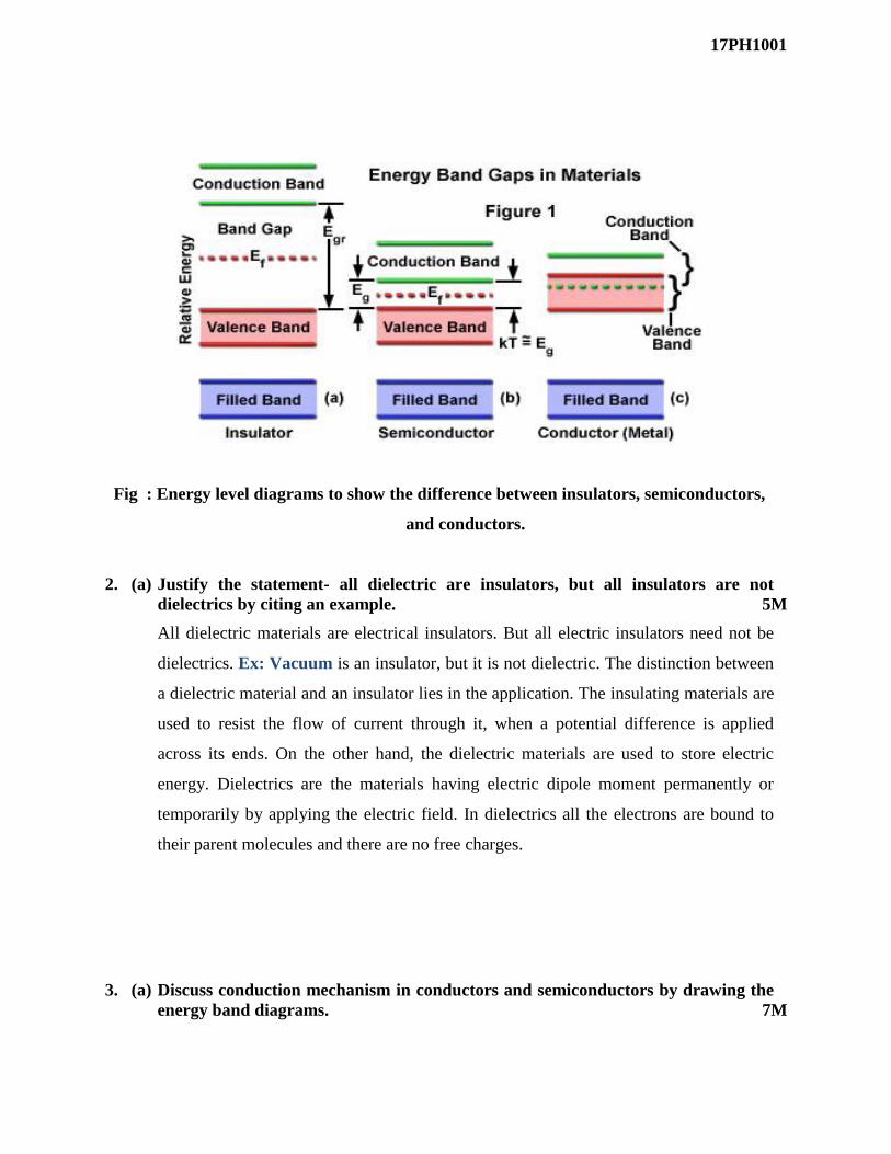
Fig : Energy level diagrams to show the difference between insulators, semiconductors,
and conductors.
2. (a) Justify the statement- all dielectric are insulators, but all insulators are not
dielectrics by citing an example. 5M
All dielectric materials are electrical insulators. But all electric insulators need not be
dielectrics. Ex: Vacuum is an insulator, but it is not dielectric. The distinction between
a dielectric material and an insulator lies in the application. The insulating materials are
used to resist the flow of current through it, when a potential difference is applied
across its ends. On the other hand, the dielectric materials are used to store electric
energy. Dielectrics are the materials having electric dipole moment permanently or
temporarily by applying the electric field. In dielectrics all the electrons are bound to
their parent molecules and there are no free charges.
3. (a) Discuss conduction mechanism in conductors and semiconductors by drawing the
energy band diagrams. 7M
17PH1001
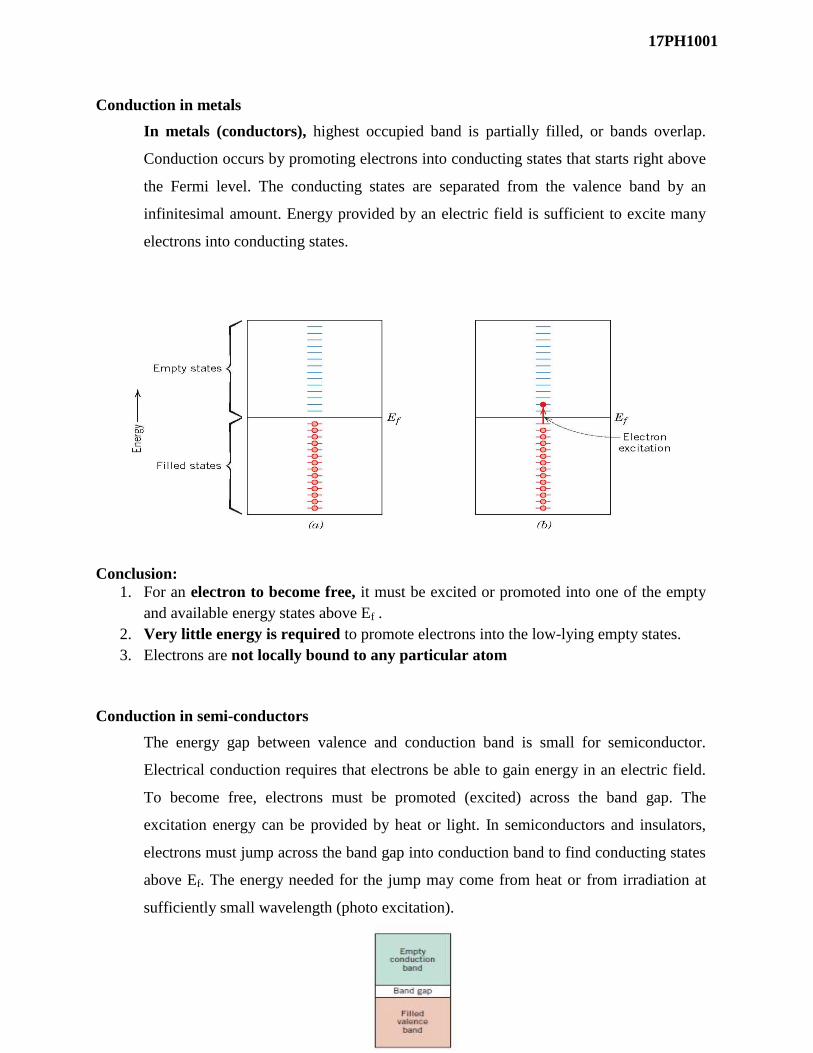
Conduction in metals
In metals (conductors), highest occupied band is partially filled, or bands overlap.
Conduction occurs by promoting electrons into conducting states that starts right above
the Fermi level. The conducting states are separated from the valence band by an
infinitesimal amount. Energy provided by an electric field is sufficient to excite many
electrons into conducting states.
Conclusion:
1. For an electron to become free, it must be excited or promoted into one of the empty
and available energy states above Ef .
2. Very little energy is required to promote electrons into the low-lying empty states.
3. Electrons are not locally bound to any particular atom
Conduction in semi-conductors
The energy gap between valence and conduction band is small for semiconductor.
Electrical conduction requires that electrons be able to gain energy in an electric field.
To become free, electrons must be promoted (excited) across the band gap. The
excitation energy can be provided by heat or light. In semiconductors and insulators,
electrons must jump across the band gap into conduction band to find conducting states
above Ef. The energy needed for the jump may come from heat or from irradiation at
sufficiently small wavelength (photo excitation).
17PH1001
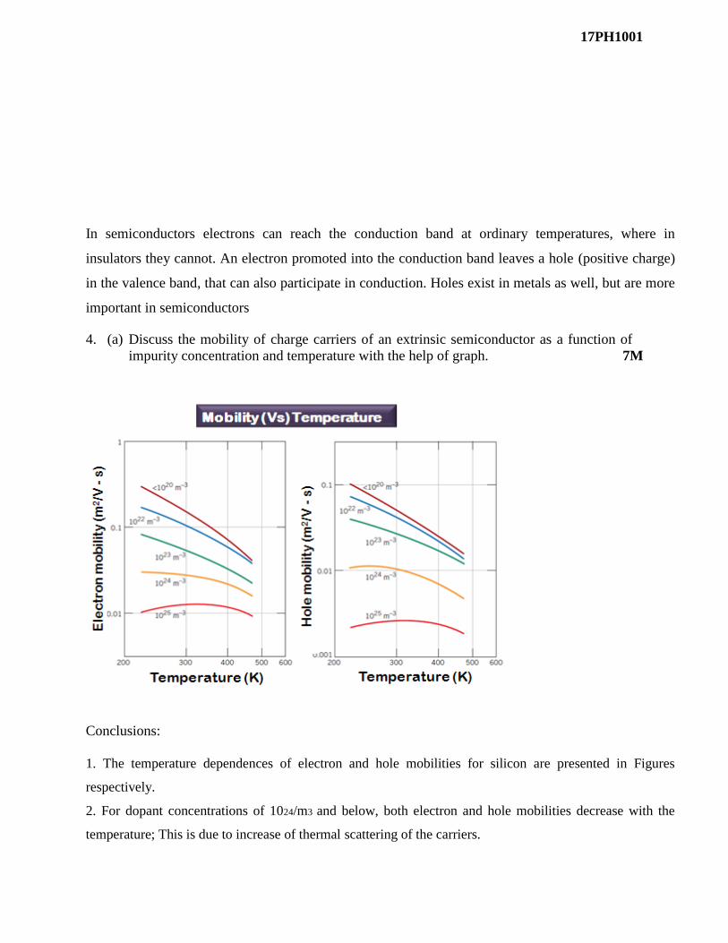
In semiconductors electrons can reach the conduction band at ordinary temperatures, where in
insulators they cannot. An electron promoted into the conduction band leaves a hole (positive charge)
in the valence band, that can also participate in conduction. Holes exist in metals as well, but are more
important in semiconductors
4. (a) Discuss the mobility of charge carriers of an extrinsic semiconductor as a function of
impurity concentration and temperature with the help of graph. 7M
Conclusions:
1. The temperature dependences of electron and hole mobilities for silicon are presented in Figures
respectively.
2. For dopant concentrations of 1024/m3 and below, both electron and hole mobilities decrease with the
temperature; This is due to increase of thermal scattering of the carriers.
17PH1001
3. For dopant concentrations of 1020/m3 and below both electrons and holes mobilities are independent of
acceptor/donor concentration
4. As the dopant concentrations increases both the plots are shifted to lower mobility values with
increasing dopant.
5. (a) Identify donor atoms and illustrate how donor impurities in semiconductors give
rise to excess free electrons compared to those generated due to valence band to
conduction band excitations. 7M
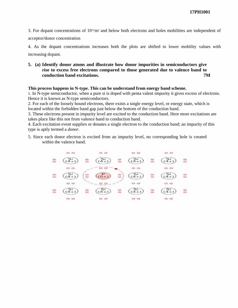
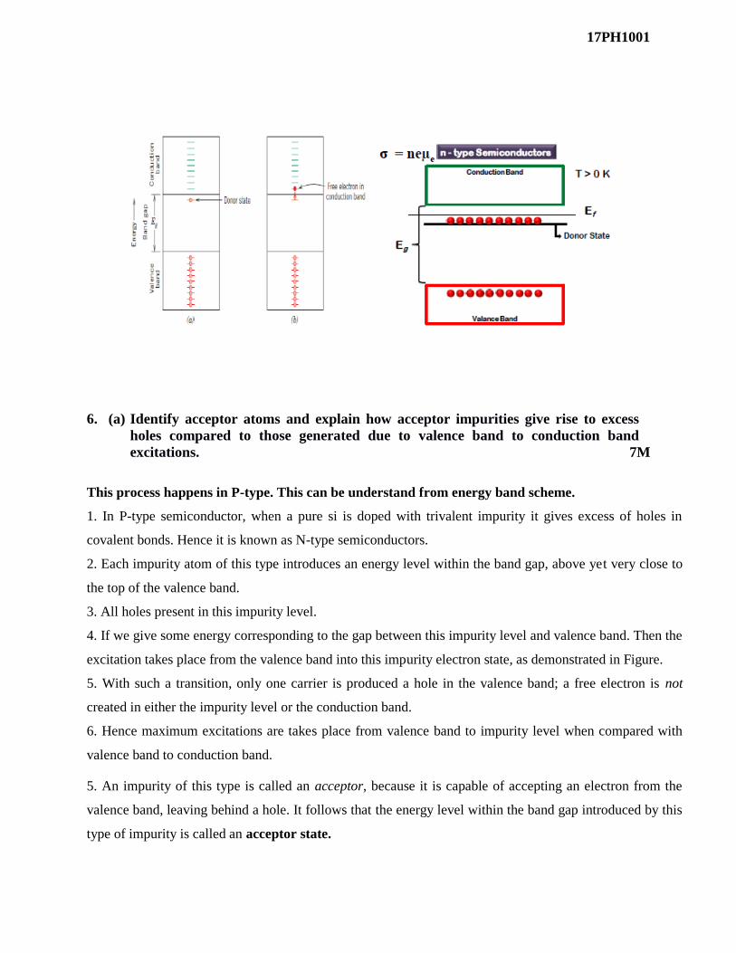
This process happens in N-type. This can be understand from energy band scheme. 1. In N-type semiconductor, when a pure si is doped with penta valent impurity it gives excess of electrons.
Hence it is known as N-type semiconductors.
2. For each of the loosely bound electrons, there exists a single energy level, or energy state, which is
located within the forbidden band gap just below the bottom of the conduction band.
3. These electrons present in impurity level are excited to the conduction band. Here more excitations are
takes place like this not from valence band to conduction band.
4. Each excitation event supplies or donates a single electron to the conduction band; an impurity of this
type is aptly termed a donor.
5. Since each donor electron is excited from an impurity level, no corresponding hole is created
within the valence band.
17PH1001
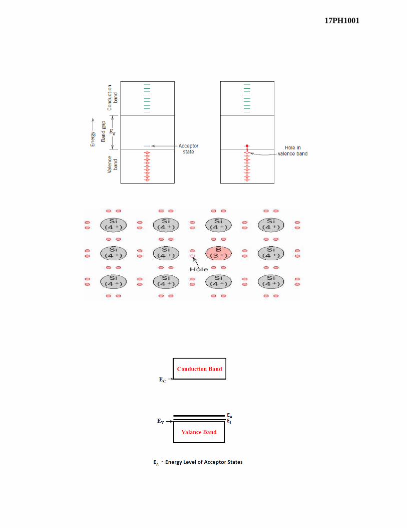
6. (a) Identify acceptor atoms and explain how acceptor impurities give rise to excess
holes compared to those generated due to valence band to conduction band
excitations. 7M
This process happens in P-type. This can be understand from energy band scheme.
1. In P-type semiconductor, when a pure si is doped with trivalent impurity it gives excess of holes in
covalent bonds. Hence it is known as N-type semiconductors.
2. Each impurity atom of this type introduces an energy level within the band gap, above yet very close to
the top of the valence band.
3. All holes present in this impurity level.
4. If we give some energy corresponding to the gap between this impurity level and valence band. Then the
excitation takes place from the valence band into this impurity electron state, as demonstrated in Figure.
5. With such a transition, only one carrier is produced a hole in the valence band; a free electron is not
created in either the impurity level or the conduction band.
6. Hence maximum excitations are takes place from valence band to impurity level when compared with
valence band to conduction band.
5. An impurity of this type is called an acceptor, because it is capable of accepting an electron from the
valence band, leaving behind a hole. It follows that the energy level within the band gap introduced by this
type of impurity is called an acceptor state.
17PH1001
17PH1001
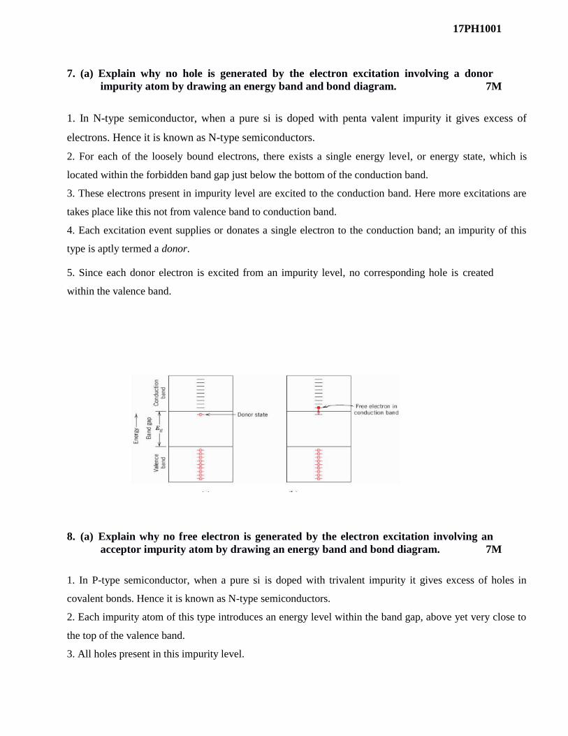
7. (a) Explain why no hole is generated by the electron excitation involving a donor
impurity atom by drawing an energy band and bond diagram. 7M
1. In N-type semiconductor, when a pure si is doped with penta valent impurity it gives excess of
electrons. Hence it is known as N-type semiconductors.
2. For each of the loosely bound electrons, there exists a single energy level, or energy state, which is
located within the forbidden band gap just below the bottom of the conduction band.
3. These electrons present in impurity level are excited to the conduction band. Here more excitations are
takes place like this not from valence band to conduction band.
4. Each excitation event supplies or donates a single electron to the conduction band; an impurity of this
type is aptly termed a donor.
5. Since each donor electron is excited from an impurity level, no corresponding hole is created
within the valence band.
8. (a) Explain why no free electron is generated by the electron excitation involving an
acceptor impurity atom by drawing an energy band and bond diagram. 7M
1. In P-type semiconductor, when a pure si is doped with trivalent impurity it gives excess of holes in
covalent bonds. Hence it is known as N-type semiconductors.
2. Each impurity atom of this type introduces an energy level within the band gap, above yet very close to
the top of the valence band.
3. All holes present in this impurity level.
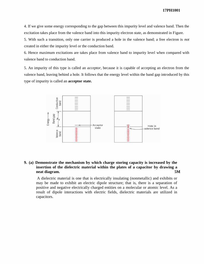
17PH1001
4. If we give some energy corresponding to the gap between this impurity level and valence band. Then the
excitation takes place from the valence band into this impurity electron state, as demonstrated in Figure.
5. With such a transition, only one carrier is produced a hole in the valence band; a free electron is not
created in either the impurity level or the conduction band.
6. Hence maximum excitations are takes place from valence band to impurity level when compared with
valence band to conduction band.
5. An impurity of this type is called an acceptor, because it is capable of accepting an electron from the
valence band, leaving behind a hole. It follows that the energy level within the band gap introduced by this
type of impurity is called an acceptor state.
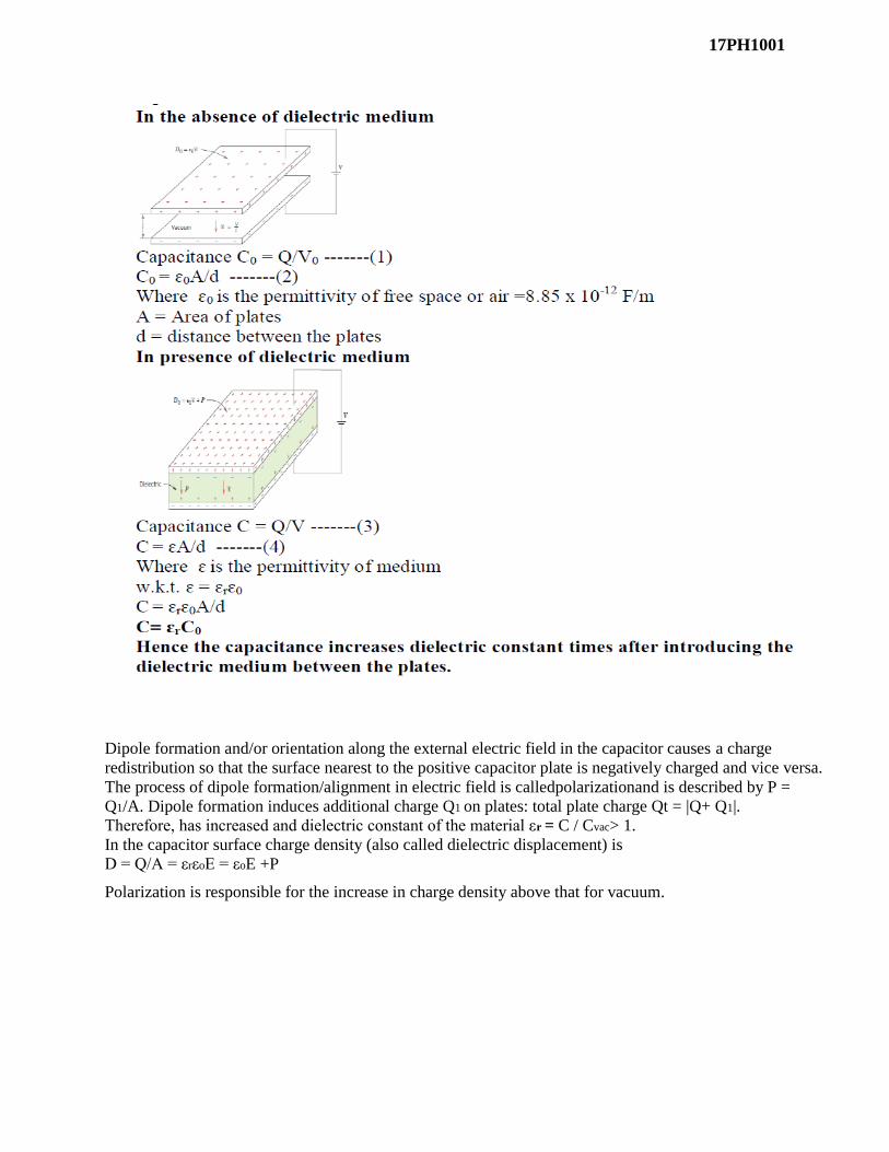
9. (a) Demonstrate the mechanism by which charge storing capacity is increased by the
insertion of the dielectric material within the plates of a capacitor by drawing a
neat diagram. 5M
A dielectric material is one that is electrically insulating (nonmetallic) and exhibits or
may be made to exhibit an electric dipole structure; that is, there is a separation of
positive and negative electrically charged entities on a molecular or atomic level. As a
result of dipole interactions with electric fields, dielectric materials are utilized in
capacitors.
17PH1001
Dipole formation and/or orientation along the external electric field in the capacitor causes a charge
redistribution so that the surface nearest to the positive capacitor plate is negatively charged and vice versa.
The process of dipole formation/alignment in electric field is calledpolarizationand is described by P =
Q1/A. Dipole formation induces additional charge Q1 on plates: total plate charge Qt = |Q+ Q1|.
Therefore, has increased and dielectric constant of the material εr = C / Cvac> 1.
In the capacitor surface charge density (also called dielectric displacement) is
D = Q/A = εrεoE = εoE +P
Polarization is responsible for the increase in charge density above that for vacuum.
17PH1001
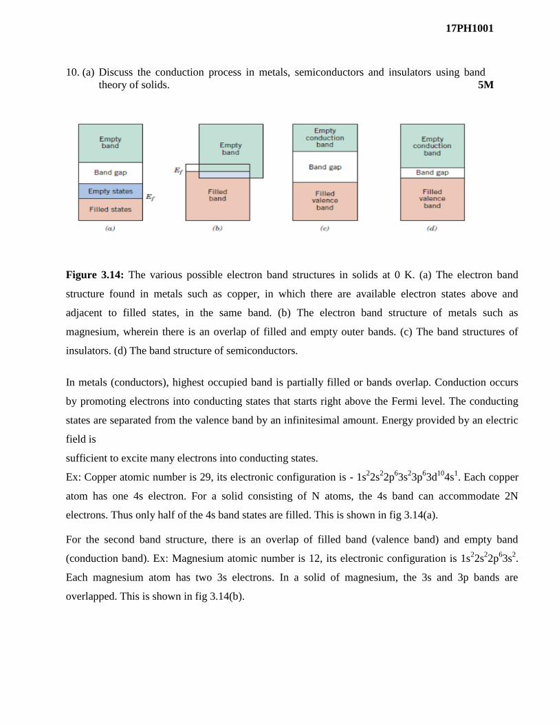
10. (a) Discuss the conduction process in metals, semiconductors and insulators using band
theory of solids. 5M
Figure 3.14: The various possible electron band structures in solids at 0 K. (a) The electron band
structure found in metals such as copper, in which there are available electron states above and
adjacent to filled states, in the same band. (b) The electron band structure of metals such as
magnesium, wherein there is an overlap of filled and empty outer bands. (c) The band structures of
insulators. (d) The band structure of semiconductors.
In metals (conductors), highest occupied band is partially filled or bands overlap. Conduction occurs
by promoting electrons into conducting states that starts right above the Fermi level. The conducting
states are separated from the valence band by an infinitesimal amount. Energy provided by an electric
field is
sufficient to excite many electrons into conducting states.
Ex: Copper atomic number is 29, its electronic configuration is - 1s22s
22p
63s
23p
63d
104s
1. Each copper
atom has one 4s electron. For a solid consisting of N atoms, the 4s band can accommodate 2N
electrons. Thus only half of the 4s band states are filled. This is shown in fig 3.14(a).
For the second band structure, there is an overlap of filled band (valence band) and empty band
(conduction band). Ex: Magnesium atomic number is 12, its electronic configuration is 1s22s
22p
63s
2.
Each magnesium atom has two 3s electrons. In a solid of magnesium, the 3s and 3p bands are
overlapped. This is shown in fig 3.14(b).
17PH1001
As shown in fig 3.14, (c) and (d) band structures are similar. The valence band is completely filled
with electrons. There is large energy gap between filled valence band and empty conduction band. Ex:
Insulators. If the energy gap between valence and conduction band is small than i.e. semiconductor.
Electrical conduction requires that electrons be able to gain energy in an electric field. To become free,
electrons must be promoted (excited) across the band gap. The excitation energy can be provided by
heat or light. In semiconductors and insulators, electrons have to jump across the band gap into
conduction band to find conducting states above Ef. The energy needed for the jump may come from
heat or from irradiation at sufficiently small wavelength (photo excitation).
The difference between semiconductors and insulators is that in semiconductors electrons can reach
the conduction band at ordinary temperatures, where in insulators they cannot. An electron promoted
into the conduction band leaves a hole (positive charge) in the valence band, that can also participate
in conduction. Holes exist in metals as well, but are more important in semiconductors and insulators.
11. (a) Explain the phenomenon of ferroelectricity and Piezoelectricity with their
applications for each. 7M
Ferroelectricity:
Ferro electricity is defined as the spontaneous alignment of electric dipoles by the mutual
interaction in the absence of an applied electric field. It arises from the fact that the local field
increases in proportion to the polarization. Thus, ferro-electric materials must possess permanent
dipoles.
Applications:
1. In optical communication, the ferro electric crystals are used for optical modulation.
2. The high dielectric constant of ferro electric crystals is also useful for storing energy
in small sized capacitors in electrical circuits.
3. These are used in electro acoustic transducers such as microphone.
Piezoelectricity:
In some ceramic materials, application of external forces produces an electric (polarization) field and
vice-versa. Applications of piezoelectricmaterials is based on conversion of mechanical strain into
electricity (microphones, strain gauges, sonar detectors) stress-free with applied stress.
Applications:
17PH1001
Cigarette lighters, depth finders, fish finders, humidifiers, jewellery cleaners, musical instruments,
speakers, telephones. Disposable patient monitors, foetal heart monitors, ultrasonic imaging
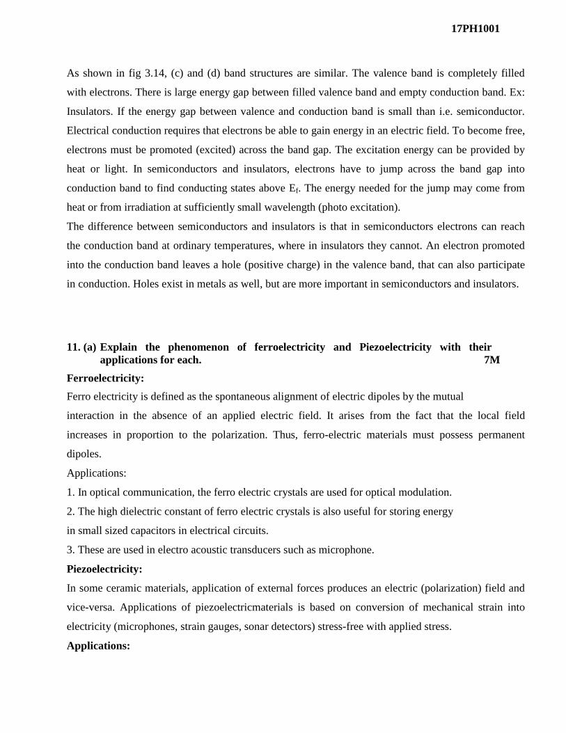
12. (a) Illustrate the relation between conductivity and mobility. Discuss Matthiessen’s
rule for metals by plotting a graph? 7M
The electrical conductivity can be expressed in terms of mobility.
σ = neµ
Thus, in general the electrical conductivity of a metal depends on two factors. They are n and
µ.
The resistivity ρ is defined by scattering events due to the imperfections and thermal
vibrations. Total resistivity ρtotal can be described by the Matthiessen’s rule:
ρtotal=ρthermal+ρimpurity+ρdeformation ,
Where ρthermal - from thermal vibrations,
ρimpurity - from impurities,
ρdeformation - from deformation-induced defects resistivity increases with temperature, with
deformation, and with alloying.
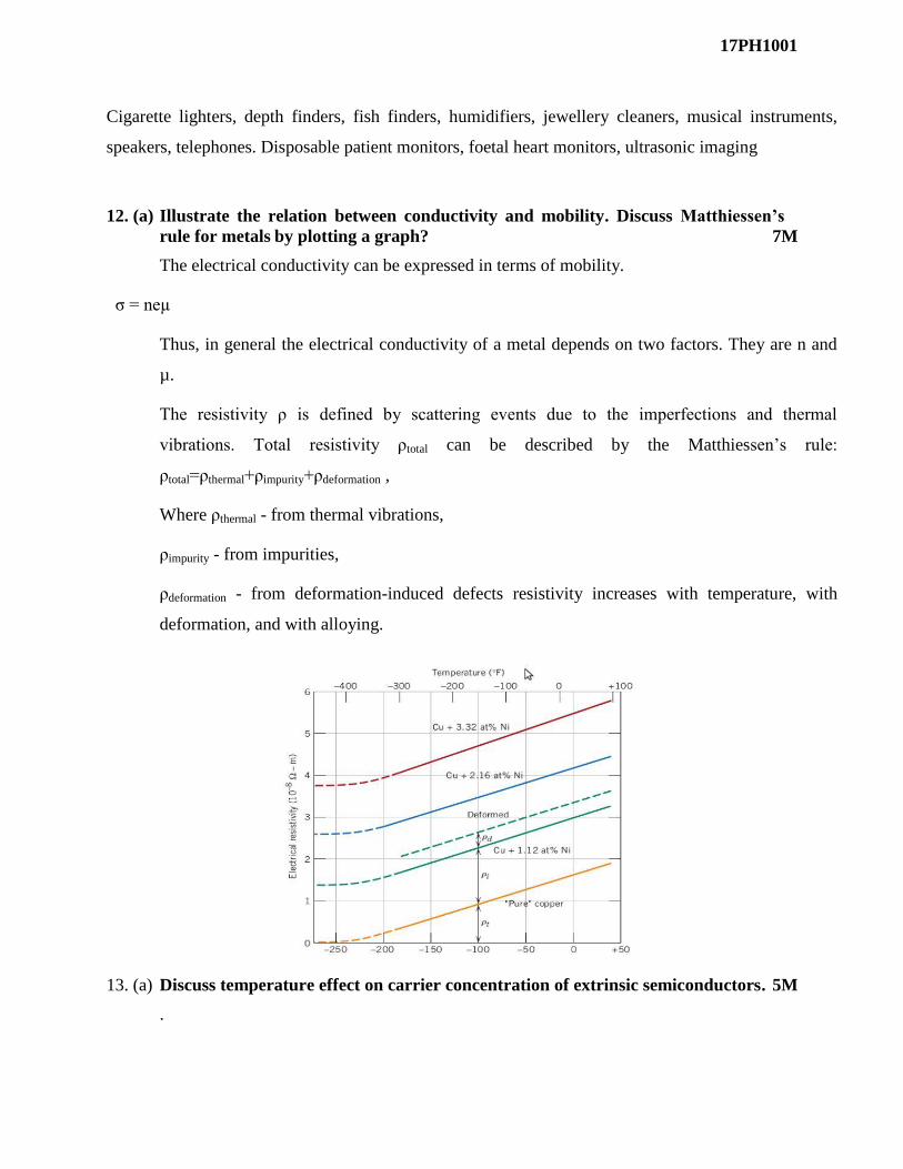
13. (a) Discuss temperature effect on carrier concentration of extrinsic semiconductors. 5M
.
17PH1001
Conclusions:
1. Electron concentration versus temperature for silicon that has been doped with phosphorus atoms is
plotted in Figure.
2. This graph has three regions.
3. First region is called as freeze-out region in which at low temperatures, below about 100 K, electron
concentration drops with decreasing temperature, and approaches zero at 0 K. here temperature is
insufficient to excite electrons from the P donor level into the conduction band.
4. Second region is called extrinsic region in which at the intermediate temperatures (between
approximately 150 K and 450 K) the material is n-type. Here electrons in the conduction band are
excited from the phosphorus donor state, and the electron concentration is approximately equal to the
P content.
5. The third region is known as intrinsic region. Here the temperature is very high and the excitations
of electrons take place from valence band to conduction band. Here along with the free electrons holes
are also produced.
17PH1001
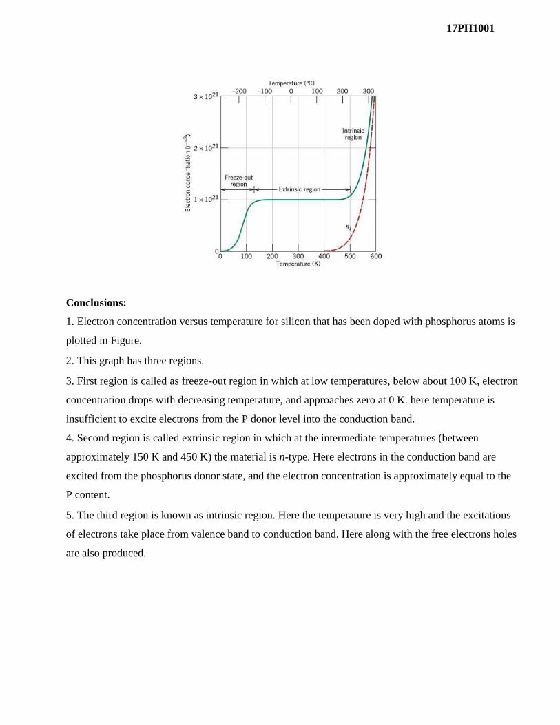
14. (a) When a dielectric material is placed inside a DC electric field, suggest that how many
ways the material gets polarized. 7M
Polarization is the alignment of permanent or induced atomic or molecular dipole
moments with an external applied electric field. There are three types of polarization
1. Electronic polarization
2. Ionic polarization
3. Molecular (orientation) polarization
Electronic polarization: it is defined as the electric strain produced in an atom due to the application of
electric field.
o It is the result of the displacement of positively charged nucleus and the electrons of an atom in opposite
directions on the application of electric field.
o This kind of polarization is present in all materials.
o It is proportional to volume of the atoms in the material.
o It is independent of temperature.
o It occurs only at optical frequencies (1015Hz)
Ionic (induced) polarization: In ionic materials, applied electric field displaces cations and
anions in opposite directions
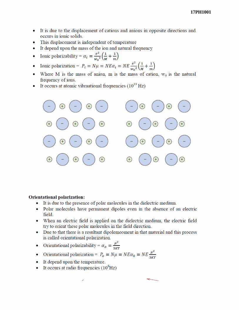
17PH1001
17PH1001
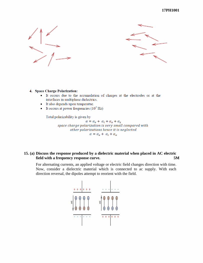
15. (a) Discuss the response produced by a dielectric material when placed in AC electric
field with a frequency response curve. 5M
For alternating currents, an applied voltage or electric field changes direction with time.
Now, consider a dielectric material which is connected to ac supply. With each
direction reversal, the dipoles attempt to reorient with the field.

17PH1001
On the application of an alternating field across the material, the polarization process occurs as
a function of time.
If a dielectric material that is subject to polarization by an ac (alternating current) electric field
With each direction reversal, the dipoles attempt to reorient with the field, in a process
requiring some finite time
Electronic polarization is extremely rapid and is complete at any instant of time even when the
frequency of the voltages is very high in optical range (1015 Hz). Thus it occurs at all
frequencies.
But ionic polarization is slower and the ions do not respond al all when the voltage corresponds
to visible optical frequencies. It occurs at atomic vibrational frequencies (1013 Hz).
The orientational polarization is much slower thanionic polarization and occurs only at radio
frequencies (108 Hz).
The space charge polarization is much slower process and it occurs at power frequencies (100
Hz).
17PH1001
16. (a) Compare the temperature dependence of the conductivity for metals and intrinsic
semiconductors. Explain the difference in behavior. 7M
In case of metals:
As the temperature increases then the resistivity of metals increases because lattice thermal vibrations
increases due to this the scattering of electrons takes place and mobility of the electrons decreases.
Hence in metals the conductivity decreases with the increase of temperature.
In case of semiconductors:
As the temperature increases, the resistivity of semiconductors decreases because the excitation
of electrons takes place from valence band to conduction band. Hence with the increase of
temperature more number of electrons and holes produced. Hence conductivity increases in
semiconductors with the increase of temperature.
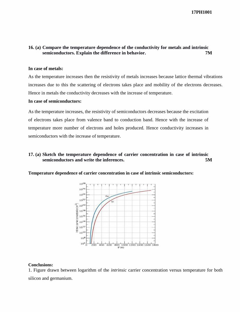
17. (a) Sketch the temperature dependence of carrier concentration in case of intrinsic
semiconductors and write the inferences. 5M
Temperature dependence of carrier concentration in case of intrinsic semiconductors:
Conclusions:
1. Figure drawn between logarithm of the intrinsic carrier concentration versus temperature for both
silicon and germanium.

17PH1001
2. The concentrations of electrons and holes increase with temperature because, with rising
temperature, more thermal energy is available to excite electrons from the valence to the conduction
band
3. At all temperatures, carrier concentration in Ge is greater than for Si.This effect is due to
germanium’s smaller band gap (Si - 0.67 versus Ge- 1.11 eV)
4. For Ge, at any given temperature more electrons will be excited across its band gap.
Temperature dependence of carrier concentration in case of extrinsic semiconductors:
Conclusions:
1. Electron concentration versus temperature for silicon that has been doped with phosphorus atoms is
plotted in Figure.
2. This graph has three regions.
3. First region is called as freeze-out region in which at low temperatures, below about 100 K, electron
concentration drops with decreasing temperature, and approaches zero at 0 K. here temperature is
insufficient to excite electrons from the P donor level into the conduction band.
17PH1001
4. Second region is called extrinsic region in which at the intermediate temperatures (between
approximately 150 K and 450 K) the material is n-type. Here electrons in the conduction band are
excited from the phosphorus donor state, and the electron concentration is approximately equal to the
P content.
5. The third region is known as intrinsic region. Here the temperature is very high and the excitations
of electrons take place from valence band to conduction band. Here along with the free electrons holes
are also produced.
18. (a) State Ohm’s law. Show that the micro and macroscopic forms of Ohm’s law are
equivalent. Discuss why the conductivity of conductor decreases with increase in
temperature where it is inverse for semiconductors. 7M
The voltage applied to a conductor which is equal to the product of current passing through the
conductor times its resistance
V= IR (Macroscopic form)
Ohm’s law in this form is independent of size and shape of the conductor under consideration.
However, it can also be expressed in terms of current density J and electric field E
J = σ E (Microscopic form)
It follows that the electric current density is proportional to the applied electric field.
Where, proportionality constant σ is called electrical conductivity.
For metals, the thermal conductivity is mainly a function of the motion of free electrons. As
the temperature increases, the molecular vibrations increase (in turn decreasing the mean free path of
molecules). So, they obstruct the flow of free electrons, thus reducing the conductivity. Semi-
conductors act as non-metals at low temperatures - the electrons are trapped within the atom. As the
temperature of the semi-conductor is increased, the electrons in the valence band gain sufficient energy
to escape from the confines of their atoms. As a result, in higher temperatures, a semi-conductor's
valence electrons are free = conduction results, resistivity decreases.