keysight 1gg7-4165 dc to 10 ghz, high output power amplifier · the 1gg7-4165 is an rf amplifier ic...
TRANSCRIPT

Keysight 1GG7-4165 DC to 10 GHz, High Output Power Amplifier
Data Sheet
Features – Usable frequency range:
DC to 10 GHz – Specified frequency range:
DC to 6 GHz – Minimum gain (S21): 13 dB – Maximum return loss (S11 and
S22): -15 dB – Output power:
P-1 : 28 dBm Psat : 29.5 dBm

Description
The 1GG7-4165 is an RF amplifier IC designed for moderately high gain, high output power, and good linearity over the DC - 6 GHz frequency range. The amplifier topology is distributed and for most applications requires off-chip termination extensions and/or chokes to supply bias and achieve flat gain down to the desired lowest desired frequency of operation. The device is fabricated using the Keysight Technologies, Inc. GaAs FET process. Solder attach is expected for most applications and the die has target alignment marks to support automatic bonding.
Absolute maximum ratings1
Symbol Parameters/conditions Min Max Units
VDD RFOUT Positive supply voltage 0 11 V
IVDD Positive supply bias current 540 mA
IRFOUT Positive supply bias current 500 mA
VGG RFIN Negative supply voltage –4.5 1.5 V
VG2AUX Second gate supply voltage –4.5 3.2 V
IG2AUX Second gate supply current 16 mA
PIN max Maximum RF input power 25 dBm
Tcase Operating case temperature –55 +90 °C
Tstg Storage temperature range –65 170 °C
Tmax Maximum assembly temperature(for 60 seconds maximum)
+300 °C
1. Parameters specified for continuous operation within Tcase limits except where noted. Operation in excess of any one of these conditions may result in performance and reliability degradation to this component. MTTF degrades by a factor 2 for every 10 degree increase in operating temperature greater than max Tcase.
DC specifications/physical properties2
Symbol Parameter/conditions Min Nom Max Units
VGG @ 300 mA VDD = 7.5 V –2.0 –1.4 –0.9 V
VGG @ 500 mA VDD = 5.0 V –1.3 –0.9 –0.5 V
Vp IDD = 25 mA –2.9 –2.2 –1.5 V
VG2aux VDD = 7.5 V 1.9 2.05 2.2 V
Idsoff VDD = 6.0 V/VGG = –3.5 V 1 1.5 2.5 mA
IdsoffVg2 VDD = 6.0 V/VG2 = –3.5 V 2.5 3.7 5 mA
2. Parameters specified at TA = 25 °C, except for temperature specs., All current polarities positive into MMIC.
– Die size: 2980 x 930 µm – Tolerance: ±10 µm – Die thickness: 127 ±15 µm – Minimum pad dimensions:
75 x 75 µm
02 | Keysight | 1GG7-4165 DC to 10 GHz, High Output Power Amplifier - Data Sheet

Frequency-domain RF specifications1, 2
VDD pad = 10 – 11 V (except where noted), IDD = 340 – 500 mA (except where noted), TA = 25 °C, Zsource = Zload = 50 ohms, OWM = on-wafer measurement
Symbol Parameter/conditions Min Nom Max Units
S21 spec OWM, 3 to 6 GHz 13 dB
S21: typical range @ 3 GHz OWM 13.8 14.7 15.5 dB
S21: typical range @ 6 GHz OWM 13.2 14.2 15 dB
S21 temp derating (approx) Packaged device on thermal chuck –0.02 –0.01 [dB/°C]
S111,2 OWM, 3 to 6 GHz, other freqs similar or better –17 –15 dB
S221,2 OWM, 6 GHz, other freqs similar or better –16 dB
Kmin 1 OWM 3 5 dB
∆PSat (50) Saturated output power roll off (2 to 6 GHz) –0.4 dB
1. Requires proper bypassing or off-chip termination extension. RF ports are AC coupled.2. Return loss is typically improved by addition of a short (~0.3 nH) bondwire.
Applications
The performance and topology of the 1GG7-4165 makes it ideal for signal source output stage applications. The IC features high output power (~28 dBm, 1 dB compressed), good harmonics, and distortion, high broadband gain (typically 14 - 15 dB, DC - 6 GHz), good gain flatness, and excellent return loss (15 dB minimum). It has low thermal resistance (~10 ° C/W soldered in a common package) making it applicable in fairly hot environments. Highest RF output power is attained at the largest allowed DC power dissipation corresponding to VDD = 11 V and IDD ~500 mA. The IC performs quite well at smaller DC dissipations – the device works well at 8 V and 300 mA, for instance. Of course, output power is not as good but gain is comparable and distortion can actually be better.
Typical integrationThe associated application diagrams give an idea of what is required of package integration depending on the lower frequency range of operation. What is common to all applications is that drain current is controlled via gate voltage (VGG). The drain power supply can be connected either at the VDD pad or through a bias circuit connected to the RFOUT pad. The VG2 pad can be left unconnected though distortion can be often improved by overriding the self bias voltage on this node.
A key challenge in package integration is making a resonance-free drain supply connec-tion capable of delivering up to around 500 mA depending on system requirements. The associated diagrams give an idea of some of the possible arrangements. Applications covering 4 to 6 GHz can usually avoid using any kind of external bypassing capacitors. The drain supply connection needs to provide a small amount of inductance (a few nH) and can easily be implemented with a few mms of 1 mil bondwire (or perhaps parallel bondwires, depending on the intended supply current). Applications covering down to 3 GHz typically require the addition of a single chip capacitor bypassing DAUX (10 pF or larger is all that is required). Frequency coverage down as low as 10 MHz can be accomplished using a good bias choke or bias tee on the drain supply and two external chip caps on the order of 800 to 1000 pF connected to the DAUX and GAUX pins.
03 | Keysight | 1GG7-4165 DC to 10 GHz, High Output Power Amplifier - Data Sheet

The bond length to the chip caps should be kept under a mm or so to avoid creating inband resonances. Coverage to lower frequencies is sometimes seen using this same topology by paralleling larger capacitors with the chip capacitors. Some deQuing might be required to avoid parallel capacitor resonances. An alternate drain supply topology is a pseudo “constant-R” network composed of a number of series L/parallel RC sections that can be arranged to effectively extend the reverse termination to arbitrarily low frequencies. The series loss of the inductors is a key issue in this kind of network and the first inductive section generally requires a thinfilm spiral, resistor and chip capacitor.
The DC operating point and environmental conditions dictate the type(s) of die attach required. For the highest power dissipation, solder die attach to a package pedestal or a metal shim is almost always the only practical choice. Thermal resistance for solder at-tach ranges from 10.0 to 11.4 ºC/W. Lower power operation can sometimes be supported with epoxy attach, but then the attach layers dominate the overall thermal resistance of the system. The associated table gives calculated thermal resistances for a few different mounting schemes. If required the thermal monitor diodes can be used to give an idea of the average die backside temperature. The plots show typical temperature-voltage relationship at a couple of currents.
Bias and Operation
Care must be taken sequencing the bias supplies on and off because full current is on the order of 800 to 1000 mA owing to the large transistor sizes. Metal traces on the die are designed to handle 540 mA from the VDD supply pad or 500 mA from the RFOUT pad al-though brief exposures to slightly higher currents may be tolerated without damage. Most insertions achieve consistent performance by designing towards operation at a particular supply current, and it is not unusual for the supply current to be monitored and actively adjusted for changes in voltage and environmental conditions. The 1GG7-4165 works as a depletion mode FET with the VDD (or RFOUT) pad acting as the drain and the VGG pad acting as the gate. Thus to avoid a large over-current situation, the VGG supply should first be powered on and driven below the expected quiescent condition. Typical VGG for 500 mA operation is –0.7 V but the expected range is from –1.0 to –0.4 V depending on the die, the drain supply voltage, and so on (PVT). Similarly for 300 mA operation, typical VGG is about –1.0 V and could range from –1.4 to –0.6 V. VG2, if it is used at all, should be kept at around 2.0 V while the drain supply is being turned up and then adjusted to its final value before readjusting VGG to recenter the drain supply current. VG2 is typically kept between 2.0 (self bias quiescent) and 3.0 V and is usually adjusted to optimize distortion. A bias point of VDD/VG2/IDD = 10.5 V/2.3 V/340 mA has been shown to have good ACPR performance. Powering down is the reverse of these steps.
RoHS Compliance
This device is RoHS Compliant. This means the component meets the requirements of the European Parliament and the Council of the European Union Restriction of Hazard-ous Substances Directive 2011/65/EU, commonly known as RoHS. The six regulated substances are lead, mercury, cadmium, chromium VI (hexavalent), polybrominated biphenyls (PBB) and polybrominated biphenyl ethers (PBDE). RoHS compliance implies that any residual concentration of these substances is below the RoHS Directive’s maximum concentration values (MVC); being less than 1000 ppm by weight for all substances except for cadmium which is less than 100 ppm by weight.
04 | Keysight | 1GG7-4165 DC to 10 GHz, High Output Power Amplifier - Data Sheet

835
595
250
0
670
320
75
930±10
70
70
2910
1505 1890 2290 29000
2980 (±12)
Figure 1. 1GG7-4165 bonding pad locations and chip dimensions (dimensions in microns)
Figure 2. 1GG7-4165 bonding and assembly diagram
Thinfilm launchor package landing
To VDD supplybias choke
1 mil wire(s)
Chip cap750 p
~1 mm
Length not important
Chip cap750 p
Chip cap750 p
Thinfilm launchor package landing
~0.4 mm
RF out
RF in
~1 mm
To VGG supply
Typical 1GG7-4165 bonding
~0.4 mm
05 | Keysight | 1GG7-4165 DC to 10 GHz, High Output Power Amplifier - Data Sheet
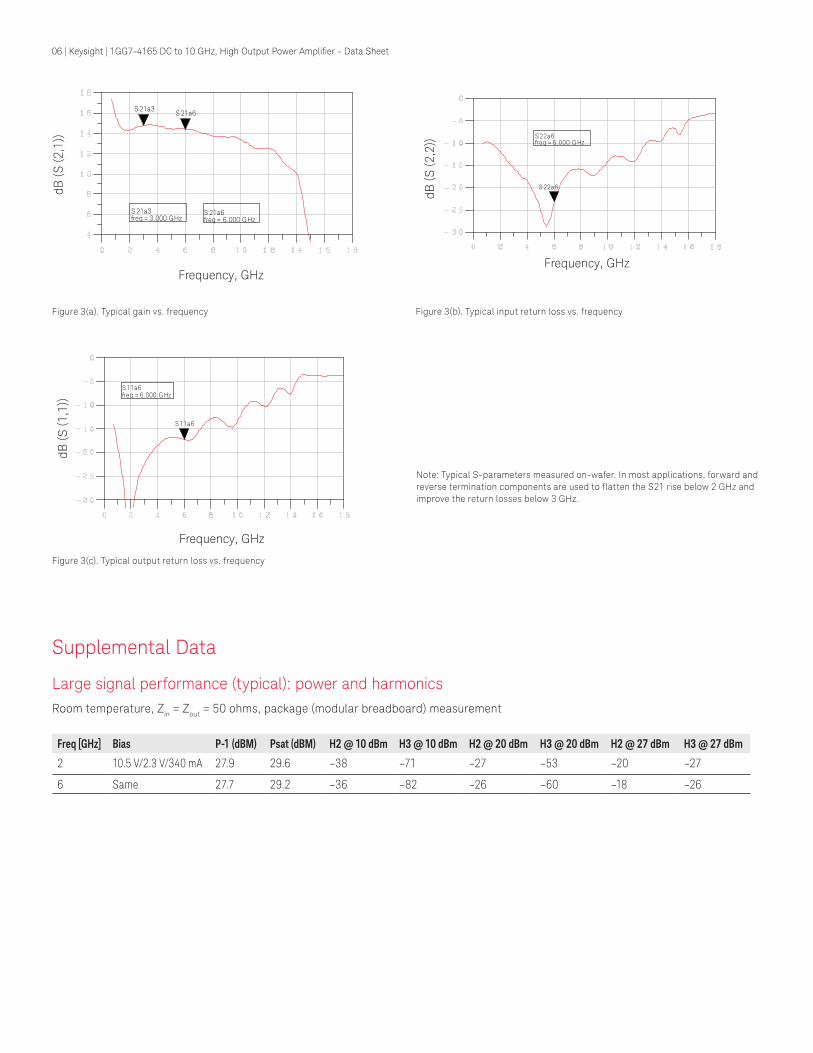
S 21a3S 21a6
S 21a3freq = 3.000 GHz
S 21a6freq = 6.000 GHz
S 11a6
S 11a6freq = 6.000 G Hz
S 22a6
S 22a6freq = 6.000 G Hz
Frequency, GHz
Frequency, GHz
Frequency, GHz
dB (S
(2,1
))
dB (S
(2,2
))
dB (S
(1,1
))
Note: Typical S-parameters measured on-wafer. In most applications, forward and reverse termination components are used to flatten the S21 rise below 2 GHz and improve the return losses below 3 GHz.
Supplemental Data
Large signal performance (typical): power and harmonicsRoom temperature, Zin = Zout = 50 ohms, package (modular breadboard) measurement
Freq [GHz] Bias P-1 (dBM) Psat (dBM) H2 @ 10 dBm H3 @ 10 dBm H2 @ 20 dBm H3 @ 20 dBm H2 @ 27 dBm H3 @ 27 dBm
2 10.5 V/2.3 V/340 mA 27.9 29.6 –38 –71 –27 –53 –20 –27
6 Same 27.7 29.2 –36 –82 –26 –60 –18 –26
Figure 3(a). Typical gain vs. frequency Figure 3(b). Typical input return loss vs. frequency
Figure 3(c). Typical output return loss vs. frequency
06 | Keysight | 1GG7-4165 DC to 10 GHz, High Output Power Amplifier - Data Sheet
-4
-3
-2
-1
0
23 24 25 26 27 28 29 30
Gai
n co
mpr
essi
on [
dB]
Pout [dBm]
Typical gain compression10.5V/2.3V/340mA
2 GHz GC
-80
-70
-60
-50
-40
-30
-20
-10
5 10 15 20 25 30
Har
mon
ic [d
BC
]
Pout [dBm]
Typical harmonics @ 6 GHz10.5 V/2.3 V/340 mA (though bias tee)
Pout@2H
Pout@3H
-80
-70
-60
-50
-40
-30
-20
-10
5 10 15 20 25 30
Har
mon
ic [d
BC]
Pout [dBm]
Typical harmonics @ 2 GHz10.5 V/2.3 V/340 mA (though bias tee)
Pout@2H
Pout@3H
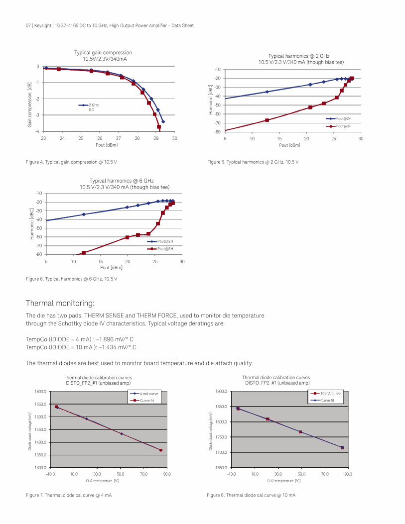
Figure 4. Typical gain compression @ 10.5 V
Figure 6. Typical harmonics @ 6 GHz, 10.5 V
Figure 7. Thermal diode cal curve @ 4 mA Figure 8. Thermal diode cal curve @ 10 mA
Figure 5. Typical harmonics @ 2 GHz, 10.5 V
Thermal monitoring:The die has two pads, THERM SENSE and THERM FORCE, used to monitor die temperature through the Schottky diode IV characteristics. Typical voltage deratings are:
TempCo (IDIODE = 4 mA) : –1.896 mV/° CTempCo (IDIODE = 10 mA ): –1.434 mV/° C
The thermal diodes are best used to monitor board temperature and die attach quality.
1300.0
1350.0
1400.0
1450.0
1500.0
1550.0
1600.0
-10.0 10.0 30.0 50.0 70.0 90.0
Dio
de s
tack
vol
tage
[mV
]
CH2 temperature [°C]
Thermal diode calibration curvesDISTO_FP2_#1 (unbiased amp)
4 mA curve
Curve fit
1650.0
1700.0
1750.0
1800.0
1850.0
1900.0
-10.0 10.0 30.0 50.0 70.0 90.0
Dio
de s
tack
vol
tage
[mV
]
CH2 temperature [°C]
Thermal diode calibration curvesDISTO_FP2_#1 (unbiased amp)
10 mA curve
Curve fit
07 | Keysight | 1GG7-4165 DC to 10 GHz, High Output Power Amplifier - Data Sheet
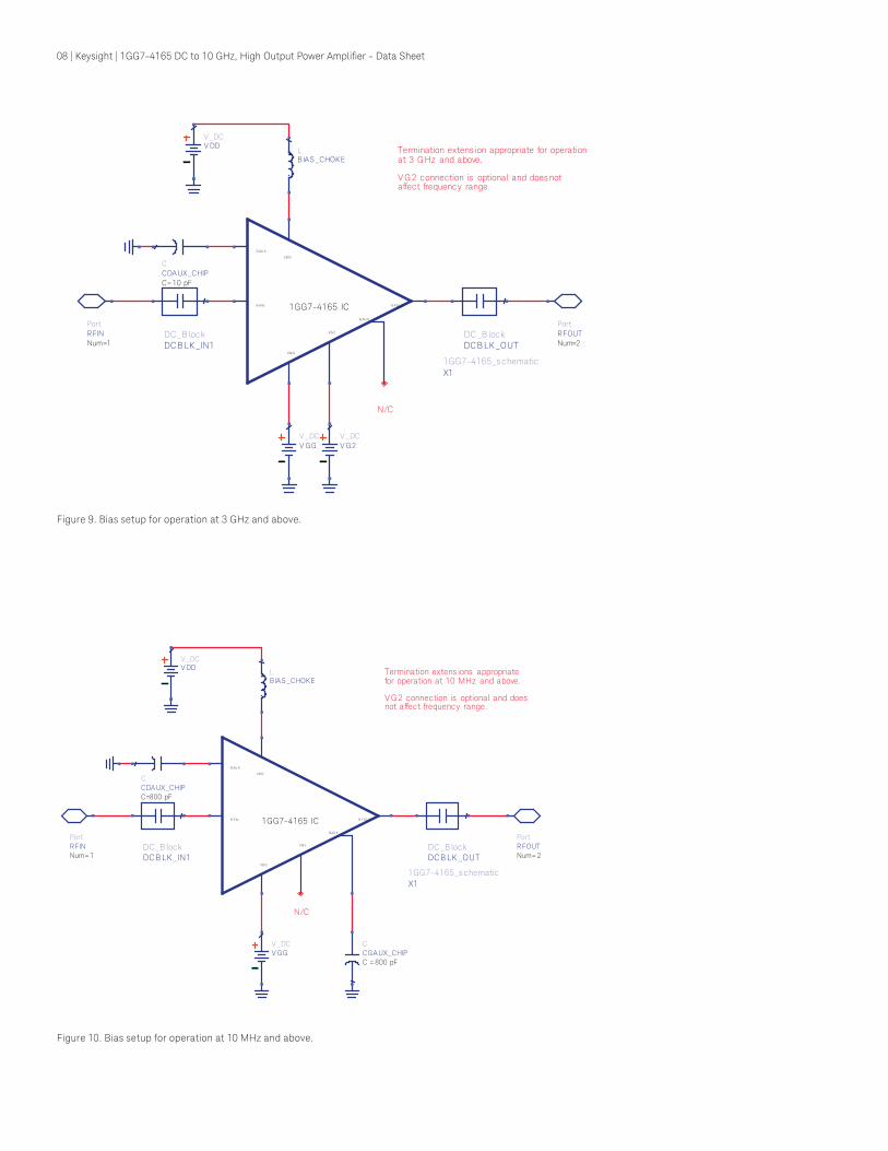
Termination extens ion appropriate for operationat 3 GHz and above.
V G2 connection is optional and does notaffect frequency range.
N/C
V _DCV G2
PortRFINNum =1
PortRFOUTNum=2
DC_B lockDCB LK _OUT
DC_B lockDCB LK _IN1
CCDAUX_CHIPC= 10 pF
1GG7-4165_s chematicX1
1GG7-4165 IC
VD D
D AU X
R FIN
VG G
VG 2
G AU X
R FOU T
V _DCV GG
V _DCV DD
LBIAS _CHOKE
Termination extens ions appropriatefor operation at 10 MHz and above.
V G2 connection is optional and doesnot affect frequency range.
N/C
PortRFINNum = 1
DC_B lockDCB LK _IN1
DC_B lockDCB LK _OUT
PortRFOUTNum = 2
CCGAUX_CHIPC = 800 pF
CCDAUX_CHIPC=800 pF
1GG7-4165_s chematicX1
1GG7-4165 IC
VD D
D AU X
R FIN
VG G
VG 2
G AU X
R FOU T
V _DCV GG
V _DCV DD
LBIAS _CHOKE
Figure 9. Bias setup for operation at 3 GHz and above.
Figure 10. Bias setup for operation at 10 MHz and above.
08 | Keysight | 1GG7-4165 DC to 10 GHz, High Output Power Amplifier - Data Sheet

Termination extens ions appropriatefor operation at 10 MHz and above.
VG2 connection is optional and doesnot affect frequency range.
N/C
N/C
V _DCV DD
PortRFOUTNum=2
B ias TeeX2
D C
R FACR FD C
PortRFINNum=1
DC_B lockDCB LK _IN1
CGAUX_CHIPC=800 pF
CDAUX_CHIPC=800 pF
1GG7-4165_schematicX1
1GG7-4165 IC
VD D
D AU X
R FIN
VG G
VG 2
G AU X
R FOU T
V _DCV GG
Constant R termination extensionappropria te for operation at the kHzrange and above.
V G 2 connection is optiona l and doesnot a ffect frequency range.
N/C
N/C
CC SMT2C =10 uF
RR D3R =36 Ohm
LLD2L=1.7 uH R
R D2R =70 Ohm
LLD1L=47 nH
LLF _C HOKE
CC GG_SMTC =100 uF
PortR F OUTNum=2
DC_B lockDCB LK _OUT
CC SMT1C =390 pF
CC DD_C HIPC =12 pF
CDAUX_C HIPC =800 pF
PortR F INNum=1
DC_B lockDCB LK _IN1
1GG7-4165_schematicX1
1GG7-4165 IC
V DD
DA UX
R FIN
V GG
V G2
GA UX
R FOUT
V_DCVDD
RR D1R =62 Ohm
LLD0L=6 nH
V_DCVGG
Figure 11. Output bias tee supply setup for operation at 10 MHz and and above.
Figure 12. Bias setup for operation at kHz range and above.
09 | Keysight | 1GG7-4165 DC to 10 GHz, High Output Power Amplifier - Data Sheet
Supplemental Data
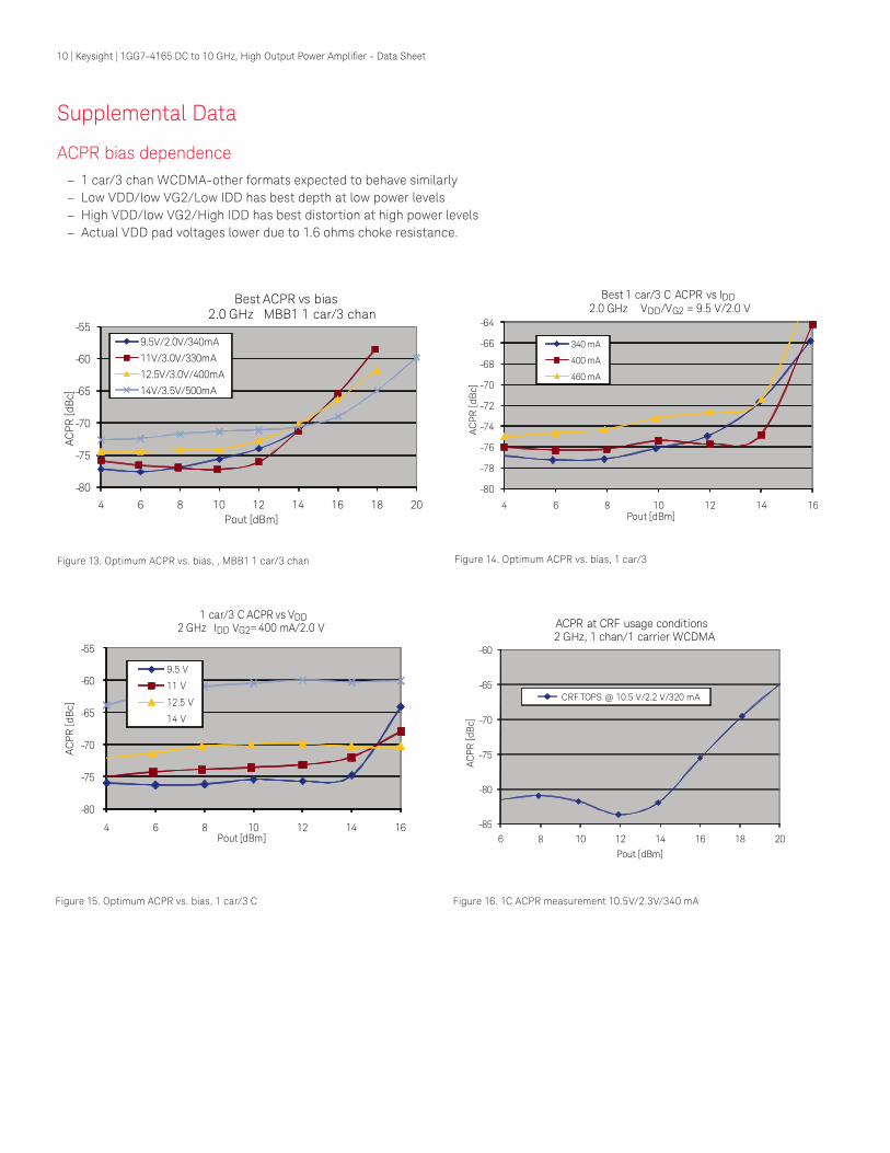
ACPR bias dependence – 1 car/3 chan WCDMA-other formats expected to behave similarly – Low VDD/low VG2/Low IDD has best depth at low power levels – High VDD/low VG2/High IDD has best distortion at high power levels – Actual VDD pad voltages lower due to 1.6 ohms choke resistance.
-80
-75
-70
-65
-60
-55
4 6 8 10 12 14 16 18 20
AC
PR [d
Bc]
Pout [dBm]
Best ACPR vs bias2.0 GHz MBB1 1 car/3 chan
9.5V/2.0V/340mA
11V/3.0V/330mA
12.5V/3.0V/400mA
14V/3.5V/500mA
-80
-78
-76
-74
-72
-70
-68
-66
-64
4 6 8 10 12 14 16
AC
PR
[dB
c]
Pout [dBm]
Best 1 car/3 C ACPR vs IDD2.0 GHz VDD/VG2 = 9.5 V/2.0 V
340 mA
400 mA
460 mA
-85
-80
-75
-70
-65
-60
6 8 10 12 14 16 18 20
AC
PR [d
Bc]
Pout [dBm]
ACPR at CRF usage conditions2 GHz, 1 chan/1 carrier WCDMA
CRF TOPS @ 10.5 V/2.2 V/320 mA
-80
-75
-70
-65
-60
-55
4 6 8 10 12 14 16
AC
PR
[dB
c]
Pout [dBm]
1 car/3 C ACPR vs VDD2 GHz IDD VG2= 400 mA/2.0 V
9.5 V
11 V
12.5 V 14 V
Figure 13. Optimum ACPR vs. bias, , MBB1 1 car/3 chan
Figure 15. Optimum ACPR vs. bias, 1 car/3 C
Figure 14. Optimum ACPR vs. bias, 1 car/3
Figure 16. 1C ACPR measurement 10.5V/2.3V/340 mA
10 | Keysight | 1GG7-4165 DC to 10 GHz, High Output Power Amplifier - Data Sheet

This data sheet contains a variety of typical and guaranteed performance data. The information supplied should not be interpreted as a complete list of circuit specifications. Customers considering the use of this, or other Keysight Technologies GaAs ICs, for their design should obtain the current production specifications from Keysight. In this data sheet the term typical refers to the 50th percentile performance. For additional information contact Keysight at [email protected].
The product described in this data sheet is RoHS Compliant. See RoHS Compliance section for more details.
11 | Keysight | 1GG7-4165 DC to 10 GHz, High Output Power Amplifier - Data Sheet
myKeysightwww.keysight.com/find/mykeysightA personalized view into the information most relevant to you.
Keysight Serviceswww.keysight.com/find/serviceKeysight Services can help from acquisition to renewal across your instrument’s lifecycle. Our comprehensive service offerings—one-stop calibration, repair, asset management, technology refresh, consulting, training and more—helps you improve product quality and lower costs.
Keysight Channel Partnerswww.keysight.com/find/channelpartnersGet the best of both worlds: Keysight’s measurement expertise and product breadth, combined with channel partner convenience.
For more information on Keysight Technologies’ products, applications or services, please contact your local Keysight office. The complete list is available at:www.keysight.com/find/contactus
Americas Canada (877) 894 4414Brazil 55 11 3351 7010Mexico 001 800 254 2440United States (800) 829 4444
Asia PacificAustralia 1 800 629 485China 800 810 0189Hong Kong 800 938 693India 1 800 11 2626Japan 0120 (421) 345Korea 080 769 0800Malaysia 1 800 888 848Singapore 1 800 375 8100Taiwan 0800 047 866Other AP Countries (65) 6375 8100
Europe & Middle EastAustria 0800 001122Belgium 0800 58580Finland 0800 523252France 0805 980333Germany 0800 6270999Ireland 1800 832700Israel 1 809 343051Italy 800 599100Luxembourg +32 800 58580Netherlands 0800 0233200Russia 8800 5009286Spain 800 000154Sweden 0200 882255Switzerland 0800 805353
Opt. 1 (DE)Opt. 2 (FR)Opt. 3 (IT)
United Kingdom 0800 0260637
For other unlisted countries:www.keysight.com/find/contactus(BP-06-08-16)
DEKRA CertifiedISO9001 Quality Management System
www.keysight.com/go/qualityKeysight Technologies, Inc.DEKRA Certified ISO 9001:2015Quality Management System
This information is subject to change without notice.© Keysight Technologies, 2016Published in USA, October 31, 20165992-1742ENwww.keysight.com
www.keysight.com/find/mmic
Evolving Our unique combination of hardware, software, support, and people can help you reach your next breakthrough. We are unlocking the future of technology.
From Hewlett-Packard to Agilent to Keysight