ki4: signal transmission in a radio system
TRANSCRIPT

KI4: SIGNAL TRANSMISSION IN A RADIO SYSTEM

DETAILED TRANSMISSION CHANNEL IN A RADIO
SYSTEM
• Pre-amp (332)• Carrier frequency in radio systems (312)• Modulation techniques (up conversion) (312)• CMOS drivers for power amplifiers in radio transmission path (332)• Band-pass filters (BPF) and their transfer function in the Laplacian domain (312)• Passive vs. active BPFs (332/312)• RF power amplifiers and its efficiency illustrated as a CMOS driver plus a BPF (332/342)• Antennas and radiation in radio systems (342)• Antenna size as a function of carrier frequency (342)

A DEMO SYSTEM – SILICON LAB SINGLE CHIP
TRANSMITTER

RADIO SPECTRUM ALLOCATION

ELECTROMAGNETIC SPECTRUM

ELECTROMAGNETIC SPECTRUM

ANTENNA EXAMPLES

ANTENNA EXAMPLES

ANTENNA EXAMPLES

DIPOLE ANTENNA RADIATION PATTERN
LOCAL OSCILLATOR
Ideal LC Tank
Real LC
Tank
0
1
LC
0 1
1
L
LQ
R
2
1 10
11 1
11
R C
LL C

LOCAL OSCILATOR
• Tuning is provided by the programmable capacitor
• Tuning range:
– 902MHz – 928MHz
– Able to compensate for 5% process variation
– Able to compensate for 2% inductance variation
• L = 17nH, Q = 30
• Output swing 1Vp-p
• Ibias = 200 – 300uA

MIXER USING SQUARE LAW
0
2
2
0
0
22
0 0
cos ,
in
': 1
2
'cos 1
2
cos
:
cos 2 cos
o o
o
D gs t ds
Q o t ds
Q o t Q o t o Q t
D Q t o Q t o
v V t LO signal
V is set not to put the FET cutoff
k WSquare Law I V V V
L
k WV V t V V
L
V V t V V V V or V V V
Expand the square term
I V V V t V V V t

MIXER USING SQUARE LAW
• The DC current from the previous equation:
• Further expand the term: 2
0cos t
2
,
'1
2D DC Q t ds
k WI V V V
L
2
0 0 0 0
1cos cos cos 1 cos 2
2t t t t
22
0 0
2 2
, 0 0
2 2
, 0 0
'cos 2 cos
2
'cos 2 cos
2
' cos cos 24 4
D Q t o Q t o
D DC o Q t o
o oD DC Q t o
k WI V V V t V V V t
L
k WI V t V V V t
L
V VWI k V V V t t
L
bias pointshift
LO modulation 2nd-order harmonics. ignore

MIXER USING SQUARE LAW
• MOSFET transconductance under large signal LO input signal:
• If Vgs follows the LO signal, then Id also follows LO signal.
' 1Dgs t ds
gs
I Wg t k V V V
V L
0
0
0
cos
' cos 1
1 cos 1
gs Q o
Q t o ds
omQ ds
Q t
V t V V t
Wg t k V V V t V
L
Vg t V
V V

MIXER USING SQUARE LAW
• Add LO and the signal at the input, we have a mixer.
• The LC tuning network at the load will only select (i.e. resonate) the desired IF signal and pass it on to the output load. All the other frequencies will be shorted by the tuning network.
0
0 0
0
1 cos cos
cos2
2
''
2 2
oo s mQ s s
Q t
mQ os sIF
G t
mQ oIFc
s G t
G to
o
G t
Vi t g t v g t V t
V V
g Vi t V t
V V
i t g Vg t
V V V
Wk V V
V k WL VV V L

MIXER USING SQUARE LAW

MIXER USING SQUARE LAW
• Real modulation using sine function:
– Sine function modulation results in a negative lower band shift and a positive upper band shift
0 0
0
0 0
0 02 2
0 0
sin2
1 1
2 2
2 2
2 2
j t j tj te e
Fourier t f t f t e dtj
F Fj j
j jF F
j j
j jF F

SIGNAL COMBINERS

SIGNAL COMBINERS

ACTIVE LOW-PASS FILTERS

ACTIVE HIGH-PASS FILTERS

ACTIVE BAND-PASS FILTERS

MONO-CHANNEL VS. STEREO TRANSMISSION
• To recover the stereo signal:
_2
_2
L R L RL channel
L R L RR channel

KI5: SIGNAL RECEIVER IN A RADIO SYSTEM

DETAILED RECEIVING CHANNEL IN A RADIO SYSTEM
• Roles of the front-end BPF in radio receiving path (selectivity, signal blocking) (312, 332)• BPF with LC ladders (312/332)• Frequency characteristics of amplifiers (312/332)• Modulation techniques (down conversion) (312)• Feedback topologies in frequency synthesizers (332)• Design of baseband LPF/BPF with RC circuits and imperfect amplifiers (312/332)• Design and characterization of receiver antenna• Design and characterization of interface between antenna and circuits (matching and transmission line modeling) (342)• Roles of discrete time signal processing (Z-transform) on future software-defined radio (312)

A DEMO SYSTEM – SILICON LAB SINGLE CHIP
RECEIVER

QUESTIONS
1. What signals does the receiver antenna “see”?
2. Assuming the receiver antenna is a dipole antenna for 433MHz signal, what should the dimension of the antenna be?
3. What is the purpose of the first BPF?
4. How would you build a simple BPF using either passive or active (Op-amps) components?

RECEIVING ANTENNA

SIGNAL FLOW IN A GENERIC RECEIVER

FILTER BASICS
4 basic filter types
Ideal low-pass filter
Practical low-pass filter

ACTIVE FILTERS
Zi
Zf
-+
Vi Vo
f
i
ZH s
Z

ACTIVE FILTERS
Bode plot
low-pass filter
1
1
1
1
1
f f
f f f
i f f
filter
f f
R R
Z j R C RH s
Z R j R C
pR C

ACTIVE FILTERS
Bode plot
band-pass filter
1 1
1
1
1 1
1
1
1 1
f
f f f
i
f
f f
R
Z j R CH s
j R CZ
j C
j R C
j R C j R C

ACTIVE FILTERS
Now, think about the op-amp has a dominant pole at pop, and assume the op-amp has a finite gain and infinite bandwidth
1
21 1
f
i
op
Z AH s A
sZ
A p
11 1
2 21 2 1
12
1 1:
1 1
2
op
op
op
f
i
filterop
A
s
pA
A sAs AA
pp
ZLPF H s
s sZAp
p

ACTIVE FILTERS
Now, we know we want high DC gain!
1
_
0
1 2
0
1 1 1
2
1 1 1
2
3
3
4
dsv m out m o
sat ds sat
p
in in equivalent in gsin ox
m ox sat v m o
op sat
v in
IA g R g r f L
V I V
R C R CR W L C
Wg C V and a g R
L
rV
L a R
VDD
RD
Rin
Cgd vout
Cgb Cgs
Vsat is a crucial parameter for trading off gain, BW, and swing.

ACTIVE FILTERS
Or, you can attack them individually!
v m outA g R
CascodingIdsL
W/LIds
folding

AMPLIFIER DESIGN PLAN
VDD
RD
Rin
Cgd vout
Cgb Cgs
• Design for gm and DC gain: Need to pick Vsatand Ids first!
2
' ' 2
' ' 22 2
ds gs t sat
dsm sat ds
sat
W WI k V V k V
L L
IW Wg k V k I
L L V
4 design variables (Ids, Vsat, gm, W/L) and 2 equations!

AMPLIFIER DESIGN PLAN
VDD
RD
Rin
Cgd vout
Cgb Cgs
• Design for gm and DC gain: Still need to pick Vsatand Ids first!
5 design variables (Ids, Vsat, gm, W/L, Vswing) and 3 equations!
2
' ' 2
' ' 22 2
2
ds gs t sat
dsm sat ds
sat
swing dd sat
W WI k V V k V
L L
IW Wg k V k I
L L V
V V V
Now, add swing constraint:

QUESTIONS
5. How does the mixer perform signal down-conversion?
6. Can the same mixer used for up-conversion perform down-conversion?
7. What is the function of the baseband amplifier
8. What is the function of the LPF at the end?

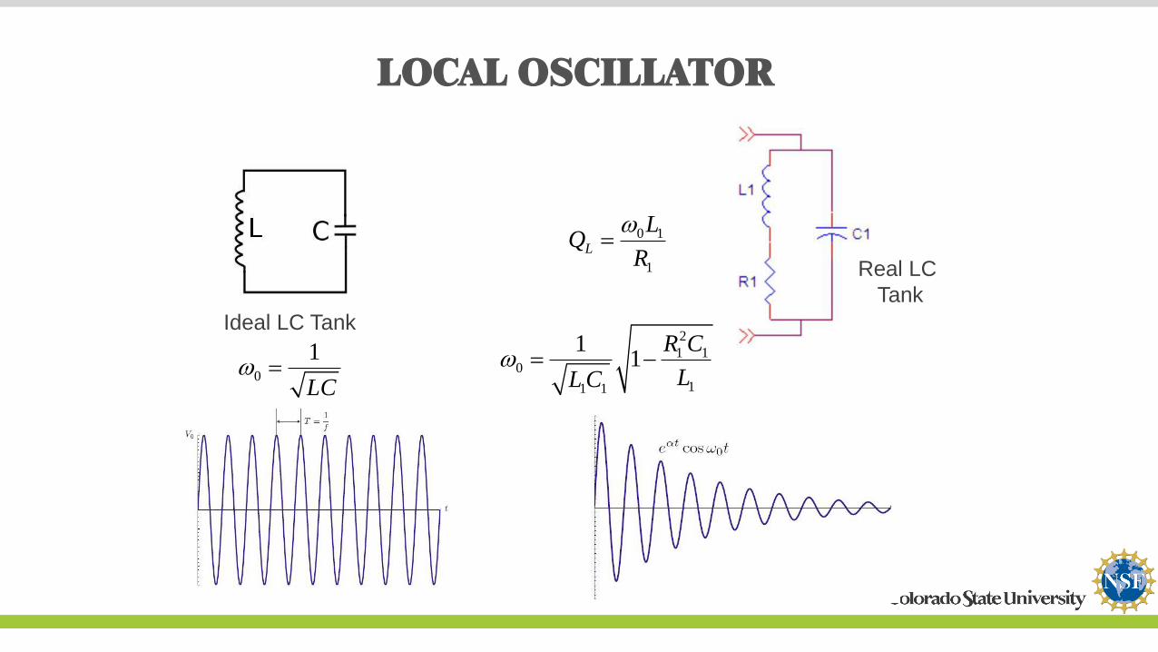
LOCAL OSCILLATOR
Ideal LC Tank
Real LC
Tank
0
1
LC
0 1
1
L
LQ
R
2
1 10
11 1
11
R C
LL C

LOCAL OSCILLATOR
• Tuning is provided by the programmable capacitor
• Tuning range:
– 902MHz – 928MHz
– Able to compensate for 5% process variation
– Able to compensate for 2% inductance variation
• L = 17nH, Q = 30
• Output swing 1Vp-p
• Ibias = 200 – 300uA

LOCAL OSCILLATOR – USE MOS VARACTOR FOR
TUNING
MOS varactor MOS varactor CV-characteristic
Tuning range

ACTIVE LOW-PASS FILTERS

ACTIVE HIGH-PASS FILTERS

ACTIVE BAND-PASS FILTERS

KI6: WRAPPING UP: THE POWER OF SMARTPHONES
Smart office!?

KI6: WHAT ENABLES THE POWER OF SMARTPHONES?
Devices/Circuits
Platforms Systems

KI6: WHAT ENABLES THE POWER OF SMARTPHONES?
Devices/Circuits
Platforms Systems

KI6: WHAT ENABLES THE POWER OF SMARTPHONES?
But the advances have been mainly driven by semiconductors and signal processing

KI6: WHAT ENABLES THE POWER OF SMARTPHONES?
Moore’s Law Scaling and Exponential Increase in Functionality

KI6: WHAT ENABLES THE POWER OF SMARTPHONES?
Moore’s Law Scaling and Exponential Increase in Functionality

KI6: WITH “FREE” TRANSISTORS, WHAT ADVANCES WERE MADE?
A lot of storage for the
exponential amount of garbage we
want to keep with us.

KI6: WITH “FREE” TRANSISTORS, WHAT ADVANCES WERE MADE?
A lot of graphics
capabilities
Qualcomm Snapdragon 820 Mobile
SOC

KI6: WITH “FREE” TRANSISTORS, WHAT ADVANCES WERE MADE?
Connectivity and speed
KI6: WITH “FREE” TRANSISTORS, WHAT ADVANCES WERE MADE?
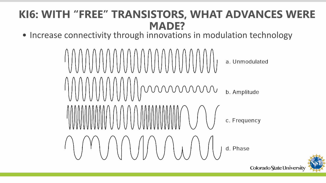
• Increase connectivity through innovations in modulation technology

KI6: WITH “FREE” TRANSISTORS, WHAT ADVANCES WERE MADE?
• AM or FM is simple but is inefficient for frequency spectrum usage
• The oscillator is used to generate carrier signal
• The simplest AM method uses a MOSFET to turn the carrier signal “on” or “off”
• The receiver uses the band-pass filter to tune to the carrier frequency.
• The diode is the simplest way for AM detection.
• If the load is a light (a simple earphone), the receiver doesn’t really need power supply as the received signal energy can drive the load directly

KI6: WITH “FREE” TRANSISTORS, WHAT ADVANCES WERE MADE?
• Limitations of AM:– AM signals are more susceptible to noise, especially weather related noise
– An AM channel only emits one signal channel (can’t do stereo)
– The receiver has poor selectivity, particularly when the carrier frequency is reasonably high.
» Hard to control the bandwidth shape (narrow) when the center frequency is increased
– Starting from the 1920s, the vacuum tubes were used to amplify the received signal to improve receiver sensitivity. However, selectivity is still the major obstacle at the time

KI6: WITH “FREE” TRANSISTORS, WHAT ADVANCES WERE MADE?
• FM:– It doesn’t rely on varying amplitudes, it doesn’t get as much noise interference
– An FM channel potentially allow for the source to emit two sub-channels of information simultaneously, allowing for left and right audio channels, perfect for stereo quality, if the carrier frequency is sufficiently high
– Short transmission distance (< 50 miles)
– Both AM and FM are analog mode of communication. They are very inefficient in the use of limited frequency spectrum.

KI6: WITH “FREE” TRANSISTORS, WHAT ADVANCES WERE MADE?
• To improve spectrum efficiency:– Modern communication relies on digital signals in the form of symbols.
– The signal bandwidth for a digital communications channel depends on the symbol rate as opposed to the bit rate.
– Phase modulation is more suited for digital signal communcation
» Binary phase shift keying (BPSK): 1 bit per symbol
» Quadrature phase shift keying (QPSK): The four symbols are +45°, +135°, -45°, and -135°.
• 2 bits per symbol
• Change in one of the bits 90 degree shift
• Change in both bits 180 degree shift
bit rate symbol rate bits per symbol
constellation diagram

KI6: WITH “FREE” TRANSISTORS, WHAT ADVANCES WERE MADE?
• To improve spectrum efficiency:– Phase modulation is more suited for digital signal communication
» Differential p/4 quadrature phase shift keying (p/4 DQPSK):
• Allow only ±p/4 and ±3p/4 for each bit change
• Can be viewed as superimposing two QPSK signal constellations offset by 45°
• To reduce complexity, during each symbol period, a phase angle from one of the QPSK constellations is transmitted. The two constellations are used alternately to transmit every pair of bits. the output demodulation rate is doubled compared to QPSK think about pipelining
• One additional (differential) bit codes which QPSK constellation giving effective 3bits/symbol

KI6: WITH “FREE” TRANSISTORS, WHAT ADVANCES WERE MADE?
• Problems with the conventional PSK schemes– Abrupt changes in carrier signal due to phase change
These abrupt changes cause harmonics extending to infinity
Produce an RF spectrum of considerable bandwidth
Not efficient for limited spectrum usage!

KI6: WITH “FREE” TRANSISTORS, WHAT ADVANCES WERE MADE?
• To improve spectrum efficiency:– Minimum shift keying (MSK)
» Continuous phase modulation scheme where the modulated carrier contains no phase discontinuities and frequency changes occur at the carrier zero crossings.
» The difference between the frequency of a logical zero and a logical one is always equal to half the data rate
• For example, a 1200 bit per second baseband MSK data signal could be composed of 1200 Hz and 1800 Hz frequencies for a logical one and zero respectively

KI6: WITH “FREE” TRANSISTORS, WHAT ADVANCES WERE MADE?
• Problems with MSK:– MSK is great for transmitting data where the data rate is relatively low compared to the channel BW
» i.e. for high data rates, it still occupy too wide of a BW for the need of current RF applications, even though it is a lot better than BPSK/QPSK.
» The spectrum energy outside the required BW mainly comes from the data source, especially when data rates are going up!

KI6: WITH “FREE” TRANSISTORS, WHAT ADVANCES WERE MADE?
• Gaussian MSK:– One solution is to forcefully reduce the spectrum energy outside the defined band (say 200KHz) by
using a pre-modulation filter
» Gaussian filter is a good candidate
» This leads to GMSK (Gaussian MSK)

KI6: WITH “FREE” TRANSISTORS, WHAT ADVANCES WERE MADE?
• 4G/LTE:– Need more performance (data rate) per channel
– 16 QAM (Quadrature Amplitude Modulation) 4-bit/symbol combination of amplitude and phase modulations.

KI6: CELLPHONE COMMUNICATION STANDARD

KI6: CELLPHONE COMMUNICATION STANDARD• TDMA (Time Division Multiple Access) used on GSM phones

KI6: WHAT ABOUT NOISE?• At the end of the receive, the quality of the signal depends on the noise level
– Carrier-to-noise ratio decreases through the receiver
– The minimum detectable signal (MDS) is when C/N ratio reaches zero.

KI6: WHAT DO AMPLIFIERS HAVE TO DO WITH ALL OF THESE?
Basebandamplifier

KI6: WHAT DO AMPLIFIERS HAVE TO DO WITH ALL OF THESE?
Class-EPower Amp

KI6: WHAT DO AMPLIFIERS HAVE TO DO WITH ALL OF THESE?
Source-degenerated Common-source LNA
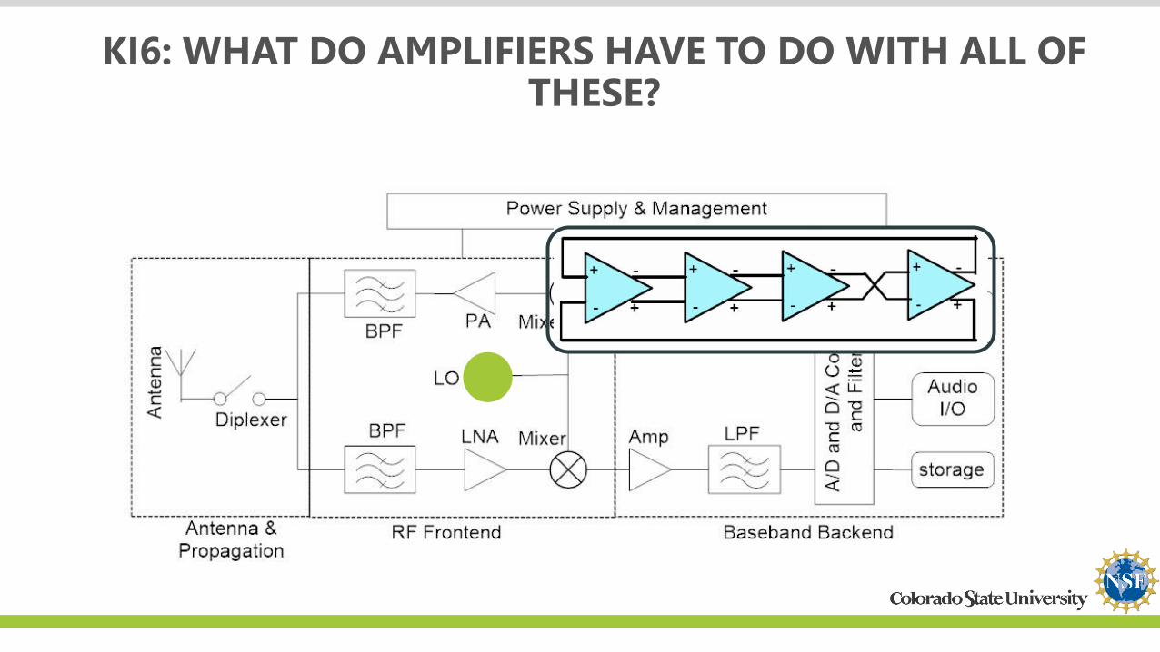
KI6: WHAT DO AMPLIFIERS HAVE TO DO WITH ALL OF THESE?

KI6: WHAT DO AMPLIFIERS HAVE TO DO WITH ALL OF THESE?

KI6: WHAT DO AMPLIFIERS HAVE TO DO WITH ALL OF THESE?
Flash ADCR-String DAC

KI6: WHAT DO AMPLIFIERS HAVE TO DO WITH ALL OF THESE?
TransimpedanceAmplifier

KI6: FUTURE OF SMARTPHONE?

LOCAL OSCILLATOR
Ideal LC Tank
Real LC
Tank
0
1
LC
0 1
1
L
LQ
R
2
1 10
11 1
11
R C
LL C

LOCAL OSCILLATOR
• Tuning is provided by the programmable capacitor
• Tuning range:
– 902MHz – 928MHz
– Able to compensate for 5% process variation
– Able to compensate for 2% inductance variation
• L = 17nH, Q = 30
• Output swing 1Vp-p
• Ibias = 200 – 300uA

LOCAL OSCILLATOR – USE MOS VARACTOR FOR TUNING
MOS varactor MOS varactor CV-characteristic
Tuning range

NOISE• Thermal noise• Shot noise• Noise 1/f• Burst noise• Transit time noise
https://en.wikipedia.org/wiki/Noise_(electronics)
Thermal noise
vrms
= 4 kBT R Df
Produced by current fluctuations due to thermal energy in electrons. It is reduced by cooling the circuit even down to LN temperatures

NOISEShot noise
Occurs when electrons have to flow across a barrier (diode). Electrons arrive individually and provoke a random fluctuation in the current.The rms value of the shot noise is given by the Schottky formula
in
= i I q Df
It occurs in almost all electronic devices. It is the consequence of a variety of phenomena like impurities in a conductive channel, or recombination in a transistor due to base current. This kind of noise is typically overshadow in electronic devices at high frequencies. The distribution is approximately Gaussian
1/f noise

BURST OR “POPCORN” NOISE
Step-like transitions between two or more discrete voltage or current levels, as high as several hundred of microvolts. It is produced by periodic trapping of carriers in impurities or in defect interfaces in the bulk. These defects can be provoked by manufacturing processes as ion implantation. Whether or not popcorn noise is a real problem, depends on your application, but when you work with small signals and low frequencies (or even DC), it is often a practical issue.
Burst or “popcorn” noise
Three OpAmps from the same kind Three precision thin film resistors plus a reference grade resistor
http://www.advsolned.com/example_popcorn_noise.html

TRANSIT-TIME NOISE
http://www.advsolned.com/example_popcorn_noise.html
When the time taken by electrons to travel from emitter to collector is comparable to the period of the signal. It is important at high frequencies and dominates over other terms

COUPLED NOISE
This is noise captured in the electronic circuits by inductive or capacitive coupling. The sources are various:
Crosstalk: signal in one channel leaks onto the signal in other channel Static noise: produced by atmospheric or natural disturbances like lightning Industrial noise: automobiles, ignition of electric motors, HV wires… Solar noise: generated in the solar corona. These electrical disturbances
generated in the Sun reaches the Earth as random EM signals Cosmic noise: produced by stars. It is smaller than the solar noise (because
the distance) but collectively (high number) can have apretiable effects

REDUCTION OF EM NOISE INFLUENCE
When building a circuit we want to avoid noises to have the true output of our circuit. Different techniques and strategies can be used to reduce the noise influence in the circuits
Faraday cage: it is an enclosure that shields the circuit from external EM noise. A Faraday cage is a grounded conductive enclosure
Avoid ground loops: ground loops generate a voltage difference between two ground nodes. Bring all ground wires to the same potential in a ground bus.
Wiring: using coaxial cables can reduce noise influence (the mesh acts as a Faraday cage). Also twisted pairs decreases the loop sizes randomizing the noise picking and reducing the overall noise signal
Filtering

NOISE: FARADAY CAGES

FFTS AND WINDOWING - TIME DOMAIN WAVEFORMS>> clear>> t = [0:255];>> om = 0.2;>> y =cos(om*t);>> stem(t,y)>> title('Original Waveform')

WINDOW FUNCTIONS
>> win1 = window(@triang,256).';>> stem(t,win1)>> title('Triangular Window')
>> win2 = hann(256).';>> stem(t,win2)>> title('Hanning Window')

WINDOWED WAVEFORMS
>> stem(t,y.*win1)>> title('Triangular Windowed Waveform')
>> stem(t,y.*win2)>> title('Hanning Windowed Waveform')

FFT AND WINDOWING>> k = [0:255];>> omg = 2*pi*k/256;>> stem(omg,abs(fft(y)))>> title('Original FFT')

FFT AND WINDOWING
>> stem(omg,abs(fft(y.*win1)))>> title('FFT with Triangular Window')
>> stem(omg,abs(fft(y.*win2)))>> title('FFT with Hanning Window')

COMPARISON BETWEEN FILTERS
ord = 4;
[zb,pb,kb] = butter(ord,1000,'s');[zc,pc,kc] = cheby1(ord,3,1000,'s');[ze,pe,ke] = ellip(ord,3,100,1000,'s');
filtb = zpk(zb,pb,kb);filtc = zpk(zc,pc,kc);filte = zpk(ze,pe,ke);
bode(filtb,filtc,filte)legend('Butterworth','Chebyshev','Elliptic')

4TH ORDER FILTERS

8TH ORDER FILTERS

FILTER COMPLEXITY – 4TH ORDER>> filtbfiltb =
1e+12------------------------------------------(s^2 + 1848s + 1e06) (s^2 + 765.4s + 1e06)
Continuous-time zero/pole/gain model.
>> tf(filtb)ans =
1e12-------------------------------------------------s^4 + 2613 s^3 + 3.414e06 s^2 + 2.613e09 s + 1e12
Continuous-time transfer function.>> filte
filte =1e-05 (s^2 + 4.687e07) (s^2 + 2.707e08)
---------------------------------------------------(s^2 + 412.7s + 1.982e05) (s^2 + 168.5s + 9.044e05)
Continuous-time zero/pole/gain model.
>> tf(filte)
ans =1e-05 s^4 + 1.783e-19 s^3 + 3176 s^2 + 1.356e-10 s + 1.269e11-------------------------------------------------------------
s^4 + 581.3 s^3 + 1.172e06 s^2 + 4.067e08 s + 1.792e11Continuous-time transfer function.

FILTER COMPLEXITY – 4TH ORDER
2nd order Butterworth LPF 4nd order Butterworth LPF

FILTER COMPLEXITY – 4TH ORDER>> filtbfiltb =
1e+24------------------------------------------------------------------------------------(s^2 + 1962s + 1e06) (s^2 + 1663s + 1e06) (s^2 + 1111s + 1e06) (s^2 + 390.2s + 1e06)
Continuous-time zero/pole/gain model.
>> tf(filtb)ans =
1e24-------------------------------------------------------------------------------------------------------------s^8 + 5126 s^7 + 1.314e07 s^6 + 2.185e10 s^5 + 2.569e13 s^4 + 2.185e16 s^3 + 1.314e19 s^2 + 5.126e21 s + 1e24
Continuous-time transfer function.
>> filtefilte =
1e-05 (s^2 + 2.183e06) (s^2 - 6.821e-13s + 2.808e06) (s^2 + 6.821e-13s + 5.595e06) (s^2 + 4.158e07)-------------------------------------------------------------------------------------------------------(s^2 + 248.5s + 6.769e04) (s^2 + 183.9s + 3.948e05) (s^2 + 101.8s + 7.679e05) (s^2 + 31.38s + 9.815e05)
Continuous-time zero/pole/gain model.>> tf(filte)
ans =1e-05 s^8 - 1.954e-19 s^7 + 521.7 s^6 - 4.348e-11 s^5 + 4.742e09 s^4 - 0.001027 s^3 + 1.45e16 s^2 - 2084 s + 1.426e22---------------------------------------------------------------------------------------------------------------------
s^8 + 565.5 s^7 + 2.318e06 s^6 + 1.06e09 s^5 + 1.739e12 s^4 + 5.862e14 s^3 + 4.436e17 s^2 + 8.663e19 s + 2.014e22Continuous-time transfer function.

FILTER COMPLEXITY – 8TH ORDER
8nd order Butterworth LPF
4nd order Butterworth LPF