layout compaction - iitkgp
TRANSCRIPT

Layout Compaction
CAD for VLSI 2
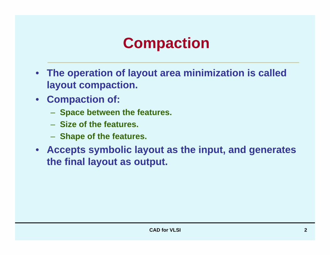
Compaction
• The operation of layout area minimization is called layout compaction.
• Compaction of:– Space between the features.– Size of the features.– Shape of the features.
• Accepts symbolic layout as the input, and generates the final layout as output.

CAD for VLSI 3
Problem Formulation
• Given:– A set of geometric features M = {M1, M2, ….., Mn}.– The minimum feature size, s(Mi), for all i.– The minimum separation between features Mi and Mj,
d(Mi,Mj).• Objective:
– Minimize the layout such thatsize(Mi) ≥ s(Mi)dist(Mi,Mj) ≥ d(Mi,Mj)
where size(Mi) and dist(Mi,Mj) are size of Mi and distance between Mi and Mj after the compaction, where 1 ≤ i,j ≤ n.
CAD for VLSI 4
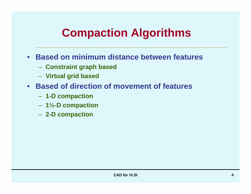
Compaction Algorithms
• Based on minimum distance between features– Constraint graph based– Virtual grid based
• Based of direction of movement of features– 1-D compaction– 1½-D compaction– 2-D compaction
CAD for VLSI 5
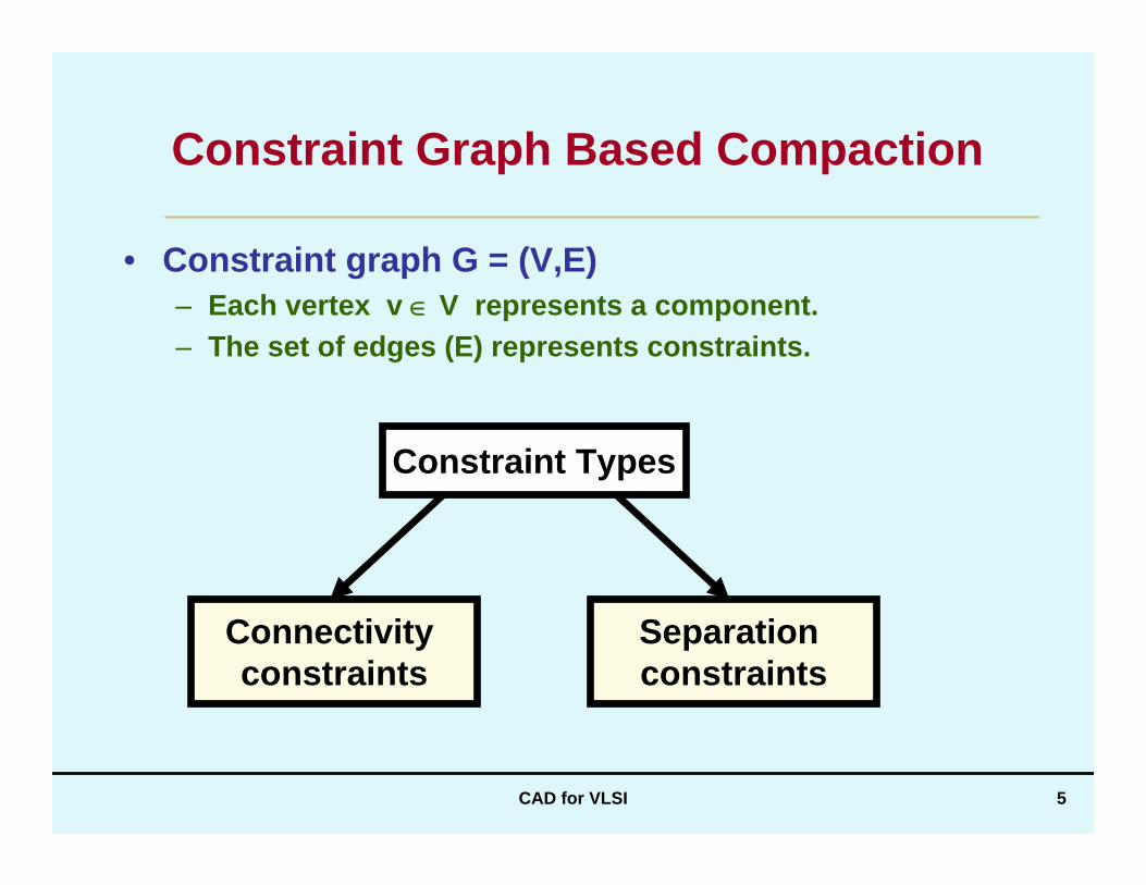
Constraint Graph Based Compaction
• Constraint graph G = (V,E)– Each vertex v ∈ V represents a component.– The set of edges (E) represents constraints.
Constraint Types
Connectivity constraints
Separation constraints
CAD for VLSI 6
Y
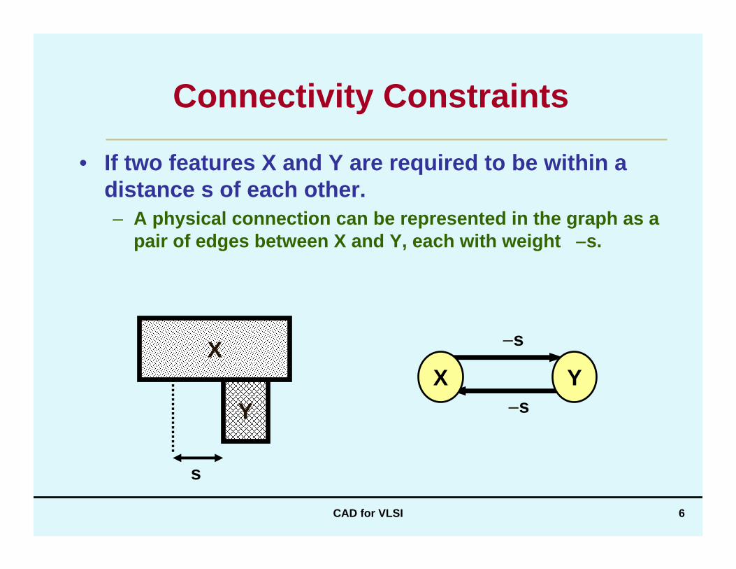
Connectivity Constraints
• If two features X and Y are required to be within a distance s of each other.– A physical connection can be represented in the graph as a
pair of edges between X and Y, each with weight −s.
XX Y
−s
−s
s
CAD for VLSI 7
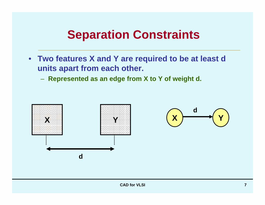
Separation Constraints
• Two features X and Y are required to be at least d units apart from each other.– Represented as an edge from X to Y of weight d.
X Y
d
X Yd

CAD for VLSI 8
The Shadow Propagation Method
• One of the best known and widely used technique for generating constraints.
• Basic idea:– The shadow of a feature is propagated along the direction
of compaction.– The shadow is caused by shining an imaginary light from
behind the feature under consideration.• The shadow is normally extended on both sides of the
feature to consider diagonal constraints.
CAD for VLSI 9
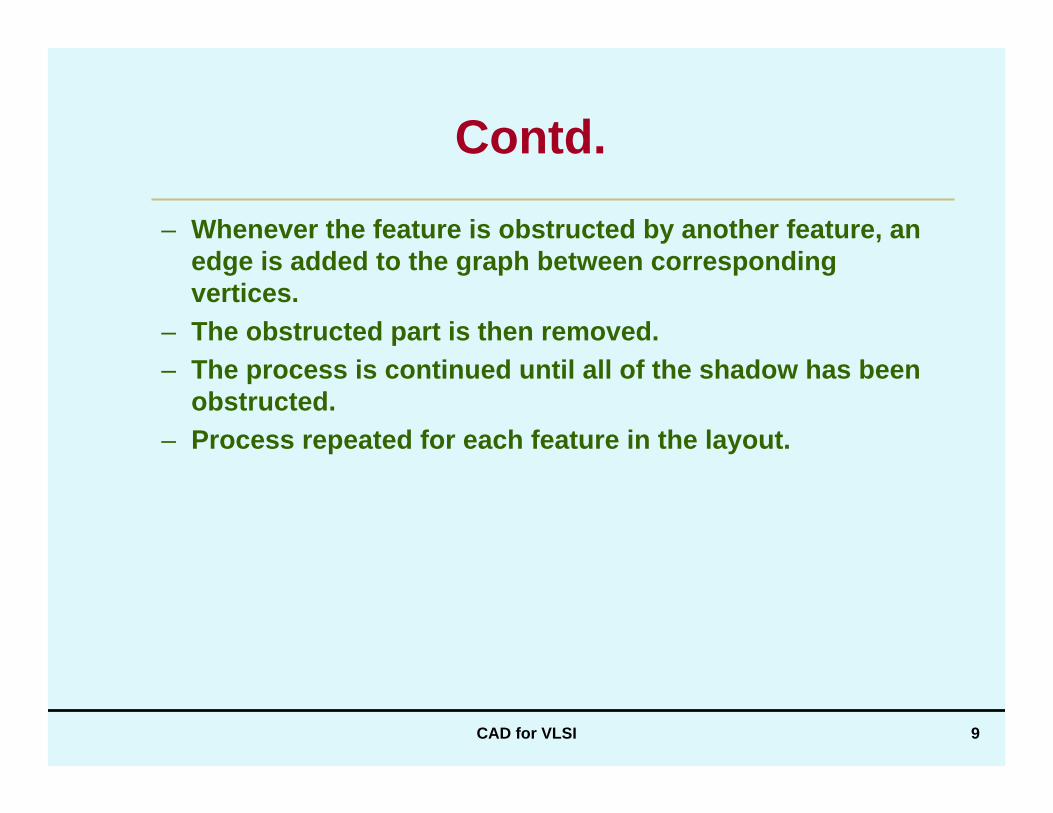
Contd.
– Whenever the feature is obstructed by another feature, an edge is added to the graph between corresponding vertices.
– The obstructed part is then removed.– The process is continued until all of the shadow has been
obstructed.– Process repeated for each feature in the layout.

CAD for VLSI 10
Example
A
B C
G H
D E
F
AD
B
GE
CAD for VLSI 11
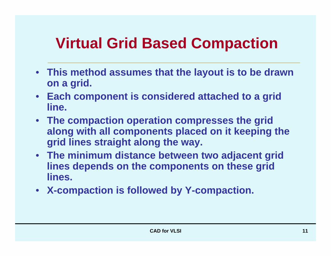
Virtual Grid Based Compaction
• This method assumes that the layout is to be drawn on a grid.
• Each component is considered attached to a grid line.
• The compaction operation compresses the grid along with all components placed on it keeping the grid lines straight along the way.
• The minimum distance between two adjacent grid lines depends on the components on these grid lines.
• X-compaction is followed by Y-compaction.

CAD for VLSI 12
Contd.
• Advantage:– Simple and easy to implement.
• Disadvantage:– Does not produce compact layouts as compared to the
constraint graph method.

CAD for VLSI 13
Example

CAD for VLSI 14
2- Dimensional Compaction
• 2-D compaction is in general much better than performing 1-D compaction.
• 2-D compaction, if solved optimally, produces minimum-area layouts.– It is very time consuming.– Thus 1½-D compaction techniques have been proposed.
• Perform x-direction compaction moves while making small moves in the y-direction.
CAD for VLSI 15
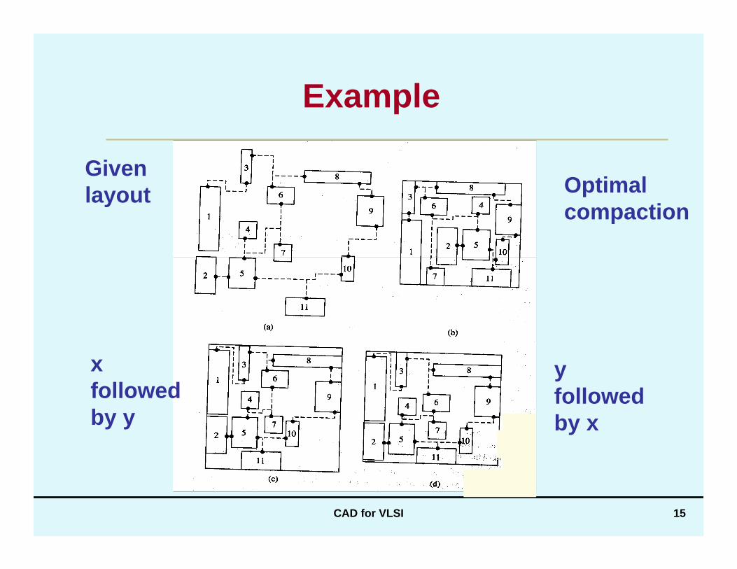
Example
x followed by y
y followed by x
Optimal compaction
Given layout
CAD for VLSI 16
1½-Dimensional Compaction
• A deterministic algorithm.– Key idea is to provide enough lateral movements to blocks
during compaction to resolve interferences.• This is called 1½-dimensional compactor, since the
geometry is not as free as in true 2-dimensional compaction.

CAD for VLSI 17
Contd.
• The algorithm maintains an X-Y adjacency graph.– Vertices represent blocks.– Edges represent horizontal and vertical adjacency.
• Two blocks have a horizontal edge if they share a vertical boundary.
• Two blocks have a vertical edge if they share a horizontal boundary.
• The labels on the edges represent the minimum allowable distance between blocks.

CAD for VLSI 18
Contd.
– Four additional vertices are added to keep all the blocks within the required bounded rectangle.
– Free space is ignored in computing the neighborhood edges between blocks.
• The algorithm assumes that the input is a partially completed layout, obtained by two applications of a 1-D compactor.

CAD for VLSI 19
Contd.
– Maintains two lists “floor” and “ceiling”.• Floor consists of all the blocks which are visible from
the top, and may become a neighbor of future block.• Ceiling is a list of all blocks which can be moved
immediately (namely, those which are visible from the bottom).
– Selects the lowest block in the ceiling list and moves it to the place on the floor which maximizes the gap between floor and ceiling.
– The process is continued until all blocks are moved from ceiling to floor.

CAD for VLSI 20
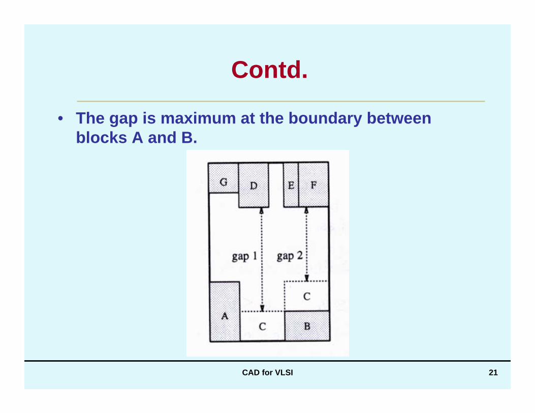
Example
• Since C is the lowest block in the ceiling list, it is selected for the move.
CAD for VLSI 21
Contd.
• The gap is maximum at the boundary between blocks A and B.
CAD for VLSI 22
Contd.
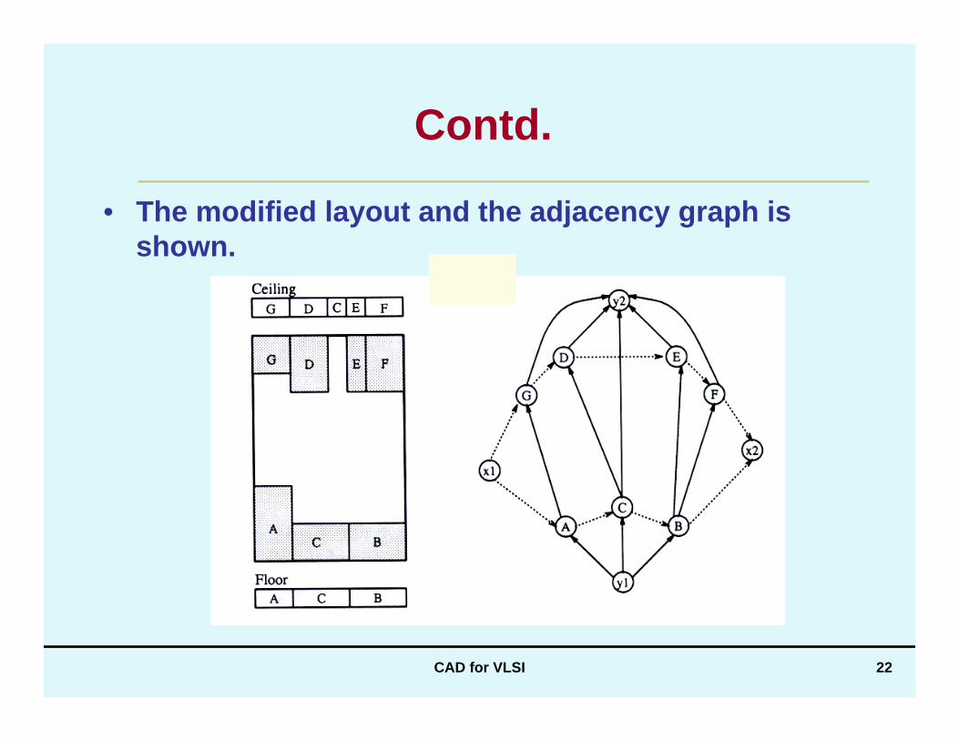
• The modified layout and the adjacency graph is shown.