ldo voltage regulator for on-chip power …jultika.oulu.fi/files/nbnfioulu-201401111002.pdf · ldo...
TRANSCRIPT
SÄHKÖTEKNIIKAN OSASTO SÄHKÖTEKNIIKAN KOULUTUSOHJELMA
LDO VOLTAGE REGULATOR FOR ON-CHIP
POWER MANAGEMENT
Author ___________________________________
Matti Tiikkainen
Supervisor ___________________________________
Timo Rahkonen
Accepted _______/_______2014
Grade ___________________________________

Tiikkainen M. (2014) LDO Voltage Regulator for On-Chip Power Management.
University of Oulu, Department of Electrical Engineering. Master’s Thesis, 86p.
ABSTRACT
In this Master's Thesis, design topologies and challenges of low-power,
integrated low-dropout regulators have been studied. Various topologies have
been examined and compared. Low-dropout regulators are commonly used in
multitude of applications, ranging from high-power systems to battery powered
mobile devices. The advantages of low-dropout regulators include simplicity,
low noise and low input-output voltage drop. The main challenge in designing
modern low-dropout regulators is achieving a high current efficiency by
reducing the quiescent current consumption of the system. In addition, the
compensation of regulators is challenging when the load current varies on a
high dynamic range.
This thesis concentrates on designing an integrated low-dropout regulator
with high dynamic range, good regulation performance and high current
efficiency. Based on the topology study, the regulator was designed around a
class AB error amplifier, the main advantage of which is the independency
between the quiescent and output currents. High dynamic performance on large
load currents was achieved by utilizing an adaptive biasing circuit for the
amplifier. In addition, a switched feedback resistor network was designed in
order to adjust the output voltage and improve the dynamic performance. The
selected circuit topologies were used to design and simulate a fully integrated
implementation and a regulator with an external capacitor in order to supply
current for a digital load.
Key words: Integrated, Low-dropout, Regulator, Quiescent current

Tiikkainen M. (2014) LDO-jänniteregulaattori piirin sisäiseen tehonhallintaan.
Oulun yliopisto, sähkötekniikan osasto. Diplomityö, 86s.
TIIVISTELMÄ
Tässä diplomityössä on tutkittu matalatehoisten, integroitujen low-dropout -
regulaattorien rakenteita sekä suunnitteluhaasteita. Työssä tutkittiin ja
vertailtiin erilaisia toteutustopologioita. Low-dropout -regulaattoreita käytetään
monenlaisissa sovelluksissa ulottuen korkeatehoisista järjestelmistä
akkukäyttöisiin mobiililaitteisiin. Low-dropout -regulaattorien etuihin kuuluvat
yksinkertaisuus, matala kohina sekä pieni tulon ja lähdön välinen jännite-ero.
Modernien low-dropout regulaattorien pääasialliset suunnitteluhaasteet
kohdistuvat korkean virtahyötysuhteen saavuttamiseen pienentämällä
lepovirtaa. Lisäksi regulaattorien kompensointi on haasteellista kun lähtövirran
vaihtelualue on laaja.
Työssä on keskitytty suunnittelemaan integroitu regulaattori, jolla on laaja
lähtövirran vaihtelualue, hyvä regulointikyky sekä korkea virtahyötysuhde.
Topologiavertailun perusteella regulaattori suunniteltiin käyttäen AB-luokan
virhevahvistinta, jonka hyöty on biasvirran ja lähtövirran riippumattomuus
toisistaan. Korkea dynaaminen suorituskyky suurilla kuormavirroilla
saavutettiin käyttämällä vahvistimen biasoinnissa adaptiivista biaspiiriä.
Lisäksi työssä suunniteltiin kytketty vastusverkko lähtöjännitteen säätämiseksi
sekä suorituskyvyn parantamiseksi. Valittuja toteutustopologioita käyttämällä
suunniteltiin kokonaan integroitu regulaattori sekä erillinen toteutus ulkoisella
lähtökondensaattorilla jotta regulaattori pystyisi ajamaan digitaalista kuormaa.
Avainsanat: Integroitu, Low-dropout, Regulaattori, Lepovirta

TABLE OF CONTENTS
ABSTRACT
TIIVISTELMÄ
TABLE OF CONTENTS
FOREWORD
LIST OF ABBREVIATIONS AND SYMBOLS
1. INTRODUCTION ................................................................................................ 9 2. FUNDAMENTALS OF LDO REGULATORS ................................................ 11
2.1. Introduction to LDO regulators .............................................................. 11 2.1.1. Dropout voltage ......................................................................... 11 2.1.2. Block level configuration .......................................................... 12
2.2. Static performance parameters ............................................................... 13
2.2.1. Efficiency .................................................................................. 13
2.2.2. Regulation performance ............................................................ 14 2.2.3. Transient characteristics ............................................................ 16
2.3. AC performance parameters ................................................................... 17 2.3.1. Frequency response ................................................................... 17
2.3.2. Power supply rejection .............................................................. 19 2.3.3. Noise .......................................................................................... 20
2.4. Design challenges ................................................................................... 21
3. EXAMINATION OF DESIGN TOPOLOGIES ................................................ 23 3.1. Series power pass device ........................................................................ 23
3.1.1. Common-drain NMOS pass device ........................................... 23 3.1.2. Common-source PMOS pass device ......................................... 26
3.1.3. Comparison of the pass device configurations .......................... 29 3.2. Charge pump .......................................................................................... 29
3.3. Error amplifier & Buffer ........................................................................ 30 3.3.1. Folded-cascode & super source follower .................................. 30 3.3.2. Class-AB amplifier .................................................................... 33
3.3.3. Comparison of error amplifiers ................................................. 36 3.4. Sensing the load current ......................................................................... 38
4. DESIGNING THE LDO .................................................................................... 39 4.1. Load conditions ...................................................................................... 39 4.2. Design considerations for the feedback loop ......................................... 40
4.2.1. Pass device characterization ...................................................... 40 4.2.2. The error amplifier .................................................................... 40
4.3. Adaptive biasing ..................................................................................... 41 4.3.1. The feedback resistors ............................................................... 43
4.4. Compensation ......................................................................................... 45 4.4.1. Small signal modeling ............................................................... 47 4.4.2. Proposed compensation scheme ................................................ 50
4.5. The charge pump .................................................................................... 51 4.6. The final LDO model ............................................................................. 52
5. PERFORMANCE EVALUATION OF THE DESIGNED LDOS .................... 53 5.1. Quiescent current consumption .............................................................. 53 5.2. Performance of the integrated LDO ....................................................... 53
5.2.1. Startup sequence ........................................................................ 53 5.2.2. Output voltage accuracy ............................................................ 54

5.2.3. Power supply rejection .............................................................. 54
5.2.4. Frequency behavior ................................................................... 56 5.2.5. Transient performance ............................................................... 58 5.2.6. Noise .......................................................................................... 61
5.3. Performance of the LDO with the external capacitor ............................. 63 5.3.1. Startup sequence ........................................................................ 63 5.3.2. Output voltage accuracy ............................................................ 63 5.3.3. Power supply rejection .............................................................. 63 5.3.4. Frequency behavior ................................................................... 65
5.3.5. Transient performance ............................................................... 67 5.3.6. Noise .......................................................................................... 71
6. DISCUSSION .................................................................................................... 73 7. CONCLUSION .................................................................................................. 76
8. REFERENCES ................................................................................................... 77 9. APPENDIX ........................................................................................................ 79

FOREWORD
This thesis was conducted at the Electronics Laboratory of the University of Oulu
and it was funded by Texas Instruments Finland. Accomplishing the thesis turned out
to be a challenging and stressful project. Completing this thesis, however, has been
invaluable in many ways. Solving the challenges along the way has been interesting
and rewarding as it has given me plenty of invaluable experience.
I would like to thank Texas Instruments Finland for the unique opportunity to do
this thesis as well as for the technical assistance. Also, I would like to thank my
supervisors, professor Timo Rahkonen from the Electronics Laboratory and Tapani
Tuikkanen from Texas Instruments Finland for their help and guidance along the
way. Finally I would like to thank my family for their unwavering support and help
throughout my studies.
Oulu, November 26. 2013
Matti Tiikkainen

LIST OF ABBREVIATIONS AND SYMBOLS
A Ampere, unit of current
AC Alternating current
CPU Central processing unit
DC Direct current
ESR Equivalent series resistance
FVF Flipped voltage follower
GBW Gain-bandwidth product
GM Gain margin
GPU Graphics processing unit
HDO High dropout
IC Integrated circuit
ICMR Input common-mode range
LDO Low dropout
NMOS N-type metal-oxide-semiconductor field-effect transistor
MOSFET Metal-oxide-semiconductor field-effect transistor
OTA Operational transconductance amplifier
PCB Printed circuit board
PM Phase margin
PMOS P-type metal-oxide-semiconductor field-effect transistor
PSR Power-supply rejection
SOC System-on-chip
SSF Super source follower
V Volt, unit of voltage
AOL LDO open-loop gain
AV Amplifier open-loop gain
BWcl Closed-loop bandwidth
Cc Compensation capacitance
Cf Fringing capacitance
Cgs Gate-to-source parasitic capacitance
Cout Output capacitance
Cox Gate capacitance per unit area
Cpar Parasitic capacitance
Cz Compensation capacitance
fp Pole frequency
fT Unity-gain frequency
fz Zero frequency
gmbs Body transconductance of a MOSFET
gmn Transconductance of n-type transistor
gmp Transconductance of p-type transistor
Iavg Average current
Iload Regulator load current
ID Drain current
Iq Quiescent current
Isr Slew-rate limited current
Kn Flicker noise parameter
L Length of the channel in field-effect transistors
Lov Overlap between gate and source junctions in MOS transistors
k Boltzmann constant
Rc Compensation resistance
rds Drain to source resistance
Req Equivalent resistance of MOSFET transistors
RFB1 Regulator feedback resistor
RFB2 Regulator feedback resistor
RL Load resistance
Ro,cp The output resistance of the charge pump
Ro,ea Error amplifier output resistance
ro,n Output resistance of n-type transistor
ro,p Output resistance of p-type transistor
Ro-pass Pass element output resistance
Ro-reg Output resistance of the regulator
T Temperature
Tp Period
TS Settling time
tsr Slew-rate time
Vdd Operation voltage
VDO Dropout voltage
VDS Drain to source voltage
VDS(sat) Saturation voltage
Veff Effective gate-source voltage
Vfb Feedback node voltage
VGS Gate to source voltage
Vin Unregulated input supply voltage
VN Noise voltage
Vout Regulated output voltage
VREF Regulator reference voltage
Vt Threshold voltage
Vtr Output voltage drop due to a load transient
W Width of the channel in field-effect transistors
ΔIload Output current change
ΔQ Total charge of a current pulse
Δt Width of a current pulse
Δt1 LDO response time
ΔVin Input voltage change
ΔVout Output voltage change
ΔVpar Voltage change associated with parasitic capacitance
η LDO efficiency
ηI Current efficiency
λ Channel-length modulation parameter
µn Mobility of electrons near silicon surface
1. INTRODUCTION
Development of low-voltage IC systems has advanced rapidly in recent years mostly
due to the evolution of mobile devices. Low-voltage requirement derives from
downscaling of IC technology and the fact that mobile devices are powered by
batteries. Even though the supply voltages are lowered, the power consumption of a
modern IC system is not necessarily low. State-of-the-art mobile phones and tablets
utilize GPUs for graphical performance and quad-core CPUs with high clock speeds.
These ICs are highly dynamic loads for power management since the device is idling
for most of the time and occasionally requires fast current pulses. These properties
create a significant challenge for power management design, since voltage regulators
should have high performance while consuming little power to conserve battery life.
Low-dropout regulators are widely used to power low-voltage IC systems because of
their accuracy, small device area and low output noise. They offer improved
efficiency over conventional regulators, due to smaller dropout voltage between
input and output terminals and lower quiescent current consumption.
Modern LDO regulators often utilize PMOS power transistors for power gating
which allows the regulator to function with a low dropout voltage. Although the
voltage drop is small, PMOS has a few drawbacks in terms of transient response and
transistor size which has increased popularity of NMOS pass devices in LDO
regulators. Degraded transient response of PMOS-gated regulators derives from high
output impedance seen in the output node. Utilizing NMOS as a power transistor
reduces the output impedance, improving the transient properties of the regulator [1].
In addition, the area of PMOS can be three times larger than NMOS due to the
difference in charge carrier mobility [2]. Since the power transistor occupies most of
the die area, minimizing its size is crucial to allow larger scale of integration. The
main disadvantage of NMOS type pass transistors is high dropout voltage which
degrades the maximum achievable efficiency. The dropout can be however lowered
by using higher gate voltage to drive the NMOS; this will be discussed in Section 3.
Conventional LDO regulators often utilize off-chip output capacitors ranging from
1 to 10 µF to ensure stability [3]. The large capacitor also improves the transient
ability of the LDO, providing or storing charge in case load current increases or
decreases rapidly. The external capacitor does however require additional PCB area
which is very limited in modern portable devices such as mobile phones and tablets.
Large off-chip capacitors are not favorable for embedded regulators in SoC
environments. This has lead to increased development of capacitorless LDO
regulators [4]. Since large capacitances cannot be integrated on-chip, the size of the
output capacitor has to be decreased. The reduction in capacitance induces two major
challenges in LDO design: stability and transient response. Since the output capacitor
has to be small, the regulator has to be compensated internally. In addition, the
regulator needs to respond quickly to fast transients since the on-chip capacitor has
limited capacity in supplying and storing charge.
The specifications of the LDO regulator designed in this thesis are presented in
Table 1.

10
Table 1. The specifications of the LDO regulator
Input Voltage 2.3 - 5.5 V
Output Voltage 1.2 - 1.8 V
Quiescent Current 150 nA
Maximum DC load current 100 mA
Output capacitor As small as possible
Startup time < 50µs
Fundamental properties of LDO regulators as well as design parameters and
challenges are discussed in Section 2. Various design topologies for realization of the
LDO are examined in Section 3. Section 4 describes the circuit level design of each
component in the design and Section 5 presents the performance evaluation of the
final design based on simulations. The schematics of the designed circuit blocks are
included as Appendices.

11
2. FUNDAMENTALS OF LDO REGULATORS
2.1. Introduction to LDO regulators
2.1.1. Dropout voltage
Linear regulators are classified as low-dropout (LDO) or high-dropout (HDO)
depending on the minimum voltage drop across the circuit. The dropout voltage is
defined as the minimum differential voltage between input and output where the
control loop stops regulating the output. The dropout voltage originates from the fact
that a series pass device, a power transistor, is connected between the input and
output of the regulator. The amount of dropout over the power transistor also dictates
the state in which the regulator operates. A linear regulator has three regions of
operation: linear, dropout and off-regions. These operational states and their
correspondence to input voltage are illustrated in Figure 1, which presents typical
input-output voltage characteristics of a linear regulator.
Figure 1. Typical input-output voltage characteristics of a LDO regulator.
In the linear region, the circuit regulates the output with a finite and nonzero loop
gain. Decreasing input voltage eventually causes one of the transistors in the control
loop to enter triode region in which the gain of the transistor is low. The regulator
still controls the output voltage, although with lower loop gain which induces some
gain error into the system. As the input voltage is decreased further, loop gain is
reduced until the system reaches its driving limit and the regulator shifts into the
dropout region. The pass device still supplies as much current as it can in order to
maintain constant output voltage. Eventually, the output voltage drops too low for
the control loop to sustain regulation. [1, 5]

12
2.1.2. Block level configuration
A linear regulator mainly consists of a control loop which senses the output voltage
and maintains a constant output voltage within a specific tolerance regardless of its
operating conditions. Figure 2 illustrates the block level composition of a NMOS
LDO regulator. The circuit comprises of a voltage reference, an error amplifier, a
power transistor and a feedback network.
Figure 2. Block-level composition of a NMOS LDO regulator.
The feedback network senses the output voltage, delivering a fraction of it to the
error amplifier input. The error amplifier compares the voltage sample to the
reference and generates an error signal which is used to drive the gate of the power
transistor. The output voltage of the regulator is determined by the reference voltage
and ratio of the output resistors RFB1 and RFB2 as
(1)
where VREF is the reference voltage and RFB1 and RFB2 are the voltage sensing
resistors.
The physical dimensions of the pass device determine the maximum amount of
current which the regulator can source to the load. Since the size of a transistor is
directly proportional to the current, the pass device has to be relatively large in order
to deliver enough current. The width and length of the channel of a MOS transistor
are determined by
(2)
where ID is the drain current, µn is the mobility of electrons near the silicon surface,
Cox is the oxide capacitance, VGS is the gate-to-source voltage and Vt is the threshold
voltage. Typically, the width of the power transistor in LDO regulators is in scale of
millimetres while the length is kept as small as the process allows. Due to the size of
the pass device, the parasitic capacitances in the transistor are relatively large. Total
capacitance at the gate can be approximated by the gate-to-source capacitance

13
(3)
where W and L are the width and length of the gate, Lov is the overlap between the
gate and the source junction and Cf is the fringing capacitance from the gate
electrode to the source.
Depending on the regulator topology, the error amplifier is either directly used to
control the pass device or a buffer is placed in between the amplifier and the power
transistor. The purpose of the buffer is to drive the highly capacitive gate of the pass
device quickly without consuming much power. Therefore, the buffer should have
low output impedance characteristics and high slew-rates to charge and discharge the
gate capacitance. Whether the gate is driven by the error amplifier alone or with the
buffer connected, the output of the amplifier should have a wide voltage swing in
order to fully open and close the pass device. The reference voltage is usually
generated by a bandgap reference. It creates a stable DC bias voltage which is
unaffected by noise, temperature and supply voltage variations. In summary, a
regulator is a structure which reacts to offset and cancels the effects of varying input
voltage, temperature and load conditions. [1, 6]
2.2. Static performance parameters
2.2.1. Efficiency
High power efficiency is essential for LDO regulators because they are commonly
utilized in battery-powered mobile applications. LDOs are inferior in efficiency
compared to their switching counterparts, which can achieve efficiencies up to 95%
[1]. This derives from the fact that voltage drop over a power switch is lower than the
voltage drop over a series power transistor [1]. Total efficiency of a LDO is
determined by the dropout voltage and current efficiency
(4)
where ηI is the current efficiency, Vin and Vout are input and output voltages, Iq is the
quiescent current and Iload is the load current. The quiescent current is the difference
between input and output current, which does not contribute to output power [5].
Most of the quiescent current in a LDO is consumed in biasing the error amplifier
and the pass device.
When the dropout voltage of the LDO is at minimum and it supplies a large
current to the load, the effect of the quiescent current is negligible and the efficiency
approaches that of a switching regulator. However, when the load current is small,
the maximum efficiency is limited by the quiescent current. Therefore, in order to
minimize battery consumption during standby, the current efficiency of the LDO
should be high. Decreasing the quiescent current however creates several design
challenges in terms of transient response and stability as slew rate of the amplifier
degrades and bandwidth of the regulator is significantly reduced.

14
2.2.2. Regulation performance
Regulation performance in LDOs is determined by line and load regulation. Load
regulation is a defined as the capability of the regulator to maintain output voltage
with varying DC changes in load current. The output voltage variation resulting from
a load current change is equivalent to the output resistance of the regulator,
(5)
where ΔVout and ΔIload are the changes in output voltage and load current, Ro-pass is
the AC output resistance of the pass transistor, AOL is the open-loop gain of the
system and β is the feedback factor [6]. Equation (5) defines that load regulation
performance is determined by the loop gain of the system.
The effect of varying output current can be analyzed with the operation point of
the pass device. Figure 3 presents NMOS I-V curve which is used to analyze DC
load regulation.
Figure 3. Analysis of load regulation using NMOS I-V curve.
In Figure 3, the regulator operates under a fixed dropout voltage VDO to maintain a
stable output voltage while the load current changes slowly in DC sense. If the load
current, which is the drain current of the NMOS transistor, drops below Iload to Iload1,
VGS will also drop in order to source a correct amount of current to the load. In
Figure 3, the transition of the operating point is from P1 to P0. If the load current
increases, VGS also has to increase accordingly. If Iload increases further, the supply
rail of the buffer will begin to limit VGS. Eventually the buffer reaches the maximum
driving voltage VGS(max) shifting the operation point to P2. Because the gate driver is
at its limit, increases in the load current shift the operating point to the right on the
VGS(max) curve. This increases the dropout voltage and eventually causes the regulator
to drop out of regulation. [2]

15
Line regulation, like load regulation, is a DC parameter which refers to the
capability of the regulator to maintain Vout with variations in Vin in a DC sense. Line
regulation can be analyzed using NMOS I-V curve illustrated in Figure 4.
Figure 4. Analysis of line regulation using NMOS I-V curve.
During operation, the regulator has to source Iload to the load while maintaining a
stable output voltage Vout even though Vin varies in DC sense. Suppose the regulator
is operating in its nominal operation point, illustrated by point P1 in Figure 4. If Vin is
increased, also VDO will increase accordingly. This increase will shift the operating
point to P2 to compensate the change in input voltage. Although the increasing input
voltage decreases efficiency, as illustrated in Equation (4), the change will not cause
the circuit any trouble as long as the input voltage is not too high to cause drain
junction of the pass transistor to breakdown. If Vin is decreased from the nominal
value, the operating point moves from P1 to P0, simultaneously decreasing VDO. The
dropout voltage can be reduced, however, only to a certain extent. In a DC sense, the
pass transistor behaves as a controllable resistance. When the operating point shifts,
also the equivalent resistance changes accordingly. Eventually Req cannot be
decreased further due to the on-resistance of the MOSFET, rds,ON. This can be
expressed as
(6)
where VGS(max) is the maximum gate-source voltage. Eventually when VDO is reduced
enough, the MOSFET enters triode region since the buffer stage cannot provide
higher driving voltage than VGS(max). Reducing VDO even further, the transistor
reaches the boundary between saturation and linear regions, illustrated as point P0 in
Figure 4. [2, 7]

16
2.2.3. Transient characteristics
Load transient response is the change in output voltage induced by a step variation in
the load current. The fluctuation is caused by the output resistance and limited
bandwidth of the regulator, as illustrated in Equation (5). The maximum tolerance for
the output voltage fluctuation varies between applications; analog electronics are
quite stringent for the operating voltage while digital circuits are far less sensitive to
variations in the supply voltage. For very sensitive analog circuits, the maximum
fluctuation can be in scale of millivolts while 1.8V logic cells tolerate approximately
0.5V voltage drops.
Figure 5 presents a typical output voltage response to a worst-case load current
variation when the regulator responds to the load change. The response is
asymmetrical because the gate driver's ability to charge and discharge the highly
capacitive input of the pass device is also asymmetrical [1].
Figure 5. Typical transient response to abrupt load current changes.
At the moment when the load current suddenly increases, the output voltage
decreases until the control loop is able to respond to the change. The time (Δt1)
required for the control loop to respond is ideally the reciprocal of the closed-loop
bandwidth but in practice it is defined by
(7)
where BWcl is the closed-loop bandwidth of the system, Cpar is the parasitic
capacitance introduced by the pass device, tsr is the slew-rate time associated with
Cpar, ΔVpar is the voltage variation at Cpar and Isr is the slew-rate limited current [8]. It
should be noted, that the slew-rate term in Equation (6) slows the response time with
a slope Isr/ Cpar, which is remarkably slow when bias currents are minimal.
Once the loop has adjusted, the output voltage settles to a level corresponding to the
new load current value, which is the difference between the ideal voltage and the
load regulation effect of the loop [1]. When load current decreases back to the
17
minimum value, the output voltage increases within Δt2. Before the control loop has
adjusted to the new load condition, the output capacitances are charged with the extra
current which the pass device still sources. After the loop has adjusted the gate of the
pass device, the regulator stops sourcing current and allows the capacitances in the
feedback loop to discharge and the output voltage slews back to its nominal value
(Δt3) [1].
Responding to a load transient becomes difficult when the current pulses drawn by
the load are fast. This is common for digital circuits which draw current on every
clock pulse. Since clock speeds are often quite high and the circuits include large
logical functionalities, the current needed from the supply is large with high slew
rates. Responding to a current pulse with a rise time of a few nanoseconds requires a
very large bandwidth from the regulator which is impossible to achieve with low
power consumption requirements. Therefore, the current pulses are outside of the
loop bandwidth and the regulator cannot react to the load change. In this case, all of
the required current is provided by the output capacitor and the voltage drop in the
output can be expressed as
(8)
where ΔQ is the total charge of the output current pulse, Iload(max) is the maximum
load current, Δt is the width of the current pulse and Cout is the output capacitance. In
order to maintain the voltage drop in acceptable levels, the output capacitor has to be
relatively large. Considering that logic current pulses for the intended application are
in order of nanoseconds and that maximum current values are in range of 100mA, the
output capacitor should be several nanofarads in order to maintain the fluctuation
below 0.5V.
The average current of a pulsed load can be approximated as
(9)
where Tp is the period of the load current. Practical values for the average load
current are around a few milliamperes, considering that the digital circuit utilizes a
5MHz clock signal. In practice the transient response of a LDO supplying a logic
circuit corresponds to a situation where the logic activity varies highly, e.g. a
situation when the logic is started or put into a standby mode.
2.3. AC performance parameters
2.3.1. Frequency response
Since the entire regulative functionality of a linear regulator is based on negative
feedback, correct frequency behavior of a LDO is crucial. Frequency response of a
LDO can be examined with a simple second order regulator model illustrated in
Figure 6. The LDO is considered as an on-chip implementation in which the output
capacitor is integrated on the silicon, thus the practical values for the output capacitor
18
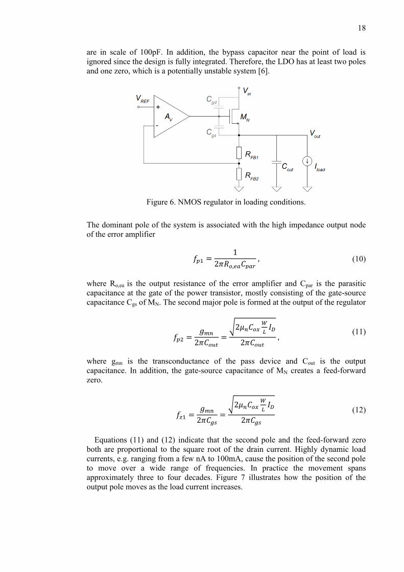
are in scale of 100pF. In addition, the bypass capacitor near the point of load is
ignored since the design is fully integrated. Therefore, the LDO has at least two poles
and one zero, which is a potentially unstable system [6].
Figure 6. NMOS regulator in loading conditions.
The dominant pole of the system is associated with the high impedance output node
of the error amplifier
(10)
where Ro,ea is the output resistance of the error amplifier and Cpar is the parasitic
capacitance at the gate of the power transistor, mostly consisting of the gate-source
capacitance Cgs of MN. The second major pole is formed at the output of the regulator
(11)
where gmn is the transconductance of the pass device and Cout is the output
capacitance. In addition, the gate-source capacitance of MN creates a feed-forward
zero.
(12)
Equations (11) and (12) indicate that the second pole and the feed-forward zero
both are proportional to the square root of the drain current. Highly dynamic load
currents, e.g. ranging from a few nA to 100mA, cause the position of the second pole
to move over a wide range of frequencies. In practice the movement spans
approximately three to four decades. Figure 7 illustrates how the position of the
output pole moves as the load current increases.

19
Figure 7. Load dependency of the second pole.
The feed-forward zero is also dependant on the load current, but since the gate-
source capacitance of MN is significantly smaller than Cout, the zero is positioned on
rather high frequencies and it cannot be used to compensate the movement of the
second pole. Therefore, the LDO is prone to instability especially on low load
currents when the two poles are separated only by a decade. On higher load currents
the pole essentially shifts outside the GBW. Although the stability is ensured on
higher loads, the phase margin (PM) of the LDO will not be sufficient for high
performance. Thus, a frequency compensation scheme should be used to stabilize the
LDO in all operation conditions and to ensure adequate PM. Compensation of LDOs
is relatively challenging since the compensation scheme should be effective
throughout the movement range of the second pole. Compensation methods for a
two-stage NMOS LDO are discussed in section 4.4.
2.3.2. Power supply rejection
Power-supply rejection (PSR) refers to the ability of a LDO to regulate its output
against small-signal AC variations in the input supply voltage [1]. Therefore, PSR is
strongly related to line regulation. The difference between the two is that line
regulation specifies only the DC variation while PSR is specified on wide range of
frequencies. PSR can be defined as the complement of supply injection, or
correspondingly as the reciprocal of supply gain Ain. The supply gain refers to the
small-signal variation in output voltage caused by small-signal changes in the input
supply [1].
(13)
where Ain is the supply gain, ∂vin and ∂vout are the small-signal changes in input and
output voltages [1].
PSR of a LDO essentially depends on the open-loop gain and bandwidth of the
regulator. Good PSR characteristics require a wide bandwidth because PSR
decreases as the frequency response rolls off. Also, signal paths from the supply to
the output of the error amplifier should be minimized since AC variation at the gate

20
of the pass device is directly seen in the output voltage. The operating voltage for the
error amplifier in NMOS LDOs is typically taken from a charge pump in order to
decrease the dropout voltage. This prevents any supply-dependent variation from
advancing through the amplifier to the gate of the pass device. Implying that the
operating voltage form the charge pump is clean, variation in the output only
depends on the gain and bandwidth. As the bandwidth of the LDO varies with the
load current, the frequency range of PSR also changes equivalently. This is
problematic when the LDO is powered down to standby since the range of sufficient
PSR decreases significantly. If the supply line is noisy and high PSR is critical for
the load circuit, the supply voltage should be filtered in order to prevent high-
frequency variation from advancing to the output. Therefore only slower variations
would remain in the supply voltage, which the LDO can suppress even with lower
bandwidth.
2.3.3. Noise
Electrical noise is a physical phenomenon which causes random current and voltage
fluctuations in the circuit formed on a fundamental level in transistors and resistors.
Behavior of noise is important since it represents the lowest signal level that can be
processed by the circuit. From the perspective of a power supply, the regulated
voltage should be as low in noise as possible since noisy supply voltages can cause
significant degradation of performance in ICs. Noise in linear regulators can be
modeled by adding an equivalent noise source for each component which contributes
to total noise in the system. Figure 9 illustrates a block diagram of a NMOS LDO
with equivalent noise sources corresponding to their respective circuit elements.
Figure 8. LDO regulator with equivalent noise sources.
Considering all the noise sources in Figure 8, the output mean-square noise can be
found with superposition [9]
21
(14)
where f1 and f2 correspond to the frequencies over which the noise is calculated, k is
the Boltzmann constant, T is temperature, β is the feedback factor RFB2/(RFB1 +
RFB2), Kn is the flicker noise parameter, VN(REF) is the reference noise and VN(EA) is
the input referenced noise of the error amplifier. For simplicity, Equation (14)
describes the amplified components only with DC closed-loop gain. In practice, the
closed loop gain has a limited bandwidth and possibly some peaking due to a
resonance at the corner frequency. Most of the noise can originate from such a
resonance peak.
As the bandgap reference noise is amplified by the error amplifier, it is typically
the dominant noise source in LDOs. The reference noise can be decreased by
inserting a RC low pass filter between the reference and the input of the error
amplifier. Decreasing the closed-loop gain (1/β) essentially reduces the total output
noise but since it also affects the output voltage, this specification cannot be changed
if the output voltage has to be fixed. The 1/f-noise of the pass device, which is
described by the second integral in Equation (14), can be reduced by increasing the
area of the transistor. The thermal noise in the system is commonly quite small
compared to the noise from active devices, but if high current efficiency is required,
the feedback resistors have to be quite large. This, in addition with the fact that the
noise from RFB2 is multiplied with the square of the closed-loop gain, implies that the
thermal noise can have a substantial effect on total noise. [9 pp. 3-4]
2.4. Design challenges
The design challenges for the NMOS regulator to be designed are listed in Table 2
Table 2. Primary design challenges
1. Low quiescent current on standby
2. Small output capacitor
3. Large dynamics in the load current
High current efficiency essentially requires that the quiescent current of the LDO is
low and moreover, precisely controllable. The error amplifier and the pass device
consume most of the quiescent current in the system as they require constant bias to
operate. Considering the total budget for the quiescent current in the design, the
amplifier should consume approximately 100nA of bias current. This obviously
constricts the dynamic performance of the amplifier significantly as bandwidth and
slew rate are dependent on the bias current. Therefore, in order to have good
performance while maintaining low static power consumption, the output current
should be independent from the biasing current. The ground current through MN
should be even smaller than the total bias current of the error amplifier. The

22
minimum current through MN is determined by the resistance of RFB2, which has to
be large in order to decrease the current below 50nA. These features induce two
problems for the design; the small transconductance of MN causes the output pole to
be pulled close to the dominant pole and the large feedback resistors can potentially
form a large time constant, affecting the settling time of the LDO.
Second design issue is the limitations of the small output capacitor in terms of
transient performance of the LDO. Integrated output capacitors in LDOs are typically
in range of 100pF due to their large area on the chip. As illustrated in Section 2.2.3,
filtering of the output voltage relies on the output capacitor when the load pulse is
outside the control loops' bandwidth. In practice this occurs when the regulator is
powered up from standby. In this case, even if the slew rate of the load current is
moderate, it is potentially outside the loop bandwidth and the output filtering relies
solely on the capacitor. As the capacitor is very small, the increasing current will
cause the output voltage to undershoot until the control loop reacts.
Large dynamics in the load current are common in digital circuits which can
consume tens of nanoamperes during standby while drawing current pulses with
magnitudes of hundreds of milliamperes during normal operation. As a consequence
of this, movement of the output pole is dramatic, potentially extending above the
GBW during high loads while pulled close to the dominating pole when load current
is low. Therefore, the compensation of the system should ensure that the LDO is
stable and has good settling characteristics regardless of the pole movement.

23
3. EXAMINATION OF DESIGN TOPOLOGIES
3.1. Series power pass device
The configuration of the output stage in linear regulators has a significant effect on
circuit performance and power efficiency. This section will introduce and evaluate
the properties of two major topologies used in linear regulators: common-source and
common-drain configurations.
3.1.1. Common-drain NMOS pass device
The dropout voltage of the common-drain configuration can be determined by
analyzing the NMOS and the transistor which drives its gate. Figure 9 illustrates the
output configuration with a PMOS supplying the current needed to charge the gate
capacitance of the NMOS. The dropout voltage is, to be specific, the minimum
headroom required to induce Iload to flow between Vin and Vout. The required voltage
over MN is the minimum source-drain voltage VSD(min) of M1 and the gate-source
voltage of MN. Thus the achievable dropout voltages with this configuration are in
order of 0.9 - 1.5V [1]. The dropout over MN can be decreased by increasing the
voltage at the gate of MN above the supply voltage Vin. This requires a separate
operating voltage for the error amplifier which is typically generated with a charge
pump.
Figure 9. Common-drain NMOS pass device configuration.
The current-sourcing terminal (i.e. the source) in NMOS regulators is attached to
Vout, as illustrated in Figure 9. This configuration has an intrinsic characteristic that
the output is a low impedance node even without a negative feedback loop [1]. The
inherent output resistance of MN in Figure 9 is approximately the reciprocal of its
transconductance. As a result, regulation performance is improved and the output
pole is pushed to higher frequencies due to the reduced time constant in the output.
This is beneficial especially in fully integrated LDO implementations because the
small output capacitor combined with the low output impedance of MN creates a high
frequency pole. As the output pole movement is less dramatic, also the compensation

24
of the LDO is easier. Load regulation of a LDO is equivalent to the open-loop output
impedance of the regulator as indicated by Equation (5). The NMOS LDO has
intrinsically higher load regulation characteristics due to the low-impedance nature
of the source follower. In addition, the feedback loop essentially decreases the output
impedance further which results in improved load regulation.
For line regulation analysis, Figure 10 illustrates a typical NMOS regulator
configuration.
Figure 10. NMOS regulator topology.
Ideally, the output voltage would stay constant regardless of the input but since the
loop gain is finite, a change in the input voltage (ΔVin) causes a variation in the
output voltage (ΔVout). Solving the line regulation from Figure 10 results in
(15)
where gmn is the transconductance of MN, ro,n is the output resistance of MN and
AV(RFB2/(RFB1+RFB2)) is the loop gain of the amplifier. Equation (15) implies that
line regulation is mainly affected by the intrinsic gain of the NMOS and the loop
gain of the amplifier. Line regulation is an equivalent phenomenon as PSR, for which
Equation (15) also defines the PSR of a NMOS regulator. The difference is that PSR
is measured over a wide range of frequencies, so the frequency behavior of MN and
the amplifier have to be considered. As with line regulation, achieving high PSR
requires sufficient gain from the error amplifier. Also, the error amplifier should
have minimum amount of signal routes from the supply line to the output of the
amplifier since AC variation at the gate of MN is directly seen at the output.
The load transient response of an ideal source follower configuration is
intrinsically improved because the source voltage drops while the gate voltage
remains stationary. This causes the current through MN to increase, thus delivering
the required current faster to the load. In practice, however, the large parasitic
capacitance Cgs causes the gate voltage to follow the source voltage, decreasing the
current through MN. The NMOS topology, does however, have the advantage of
small open-loop output impedance which essentially improves the transient
performance. Figure 11 presents a typical load transient response for a NMOS
regulator.

25
Figure 11. Load transient response of a NMOS LDO.
Output voltage variation arising from line transient is caused by signal feeding
through MN and finite loop gain. The magnitude of under- and overshoot in the
output voltage during a line transient can be approximated similarly as line
regulation in Equation (15). The extent of the variation in the output is roughly
determined by the intrinsic gain of MN and the gain of the error amplifier. Figure 12
illustrates a typical line transient response for a NMOS regulator.
Figure 12. Line transient response of a NMOS regulator.
The silicon area of LDO regulators is mostly occupied by the series power
transistor. In order to source enough current to the load, the width-length ratio has to
be relatively large. The drain current of a MOS transistor is determined by
(16)
where λ is the channel-length modulation parameter and VDS is the drain-source
voltage. One of the major advantages of the NMOS topology is the faster mobility of

26
charge carriers than in the PMOS topology. The mobility of electrons is typically two
or three times greater than the mobility of holes. Therefore, in order to achieve
similar performance as a NMOS regulator, the pass device in the PMOS topology
has to be significantly larger.
3.1.2. Common-source PMOS pass device
The drawback in the NMOS topology is that it requires a higher operating voltage for
the error amplifier in order to reach low dropout voltages. Common-source PMOS
topology, however, can achieve a low dropout without any excess circuitry. Figure
13 illustrates a common-source configuration with the driving transistor included. In
this case the input voltage only has to be VSD(sat) over the output voltage to sustain
Iload without MP drifting into the triode region. Typically the dropout for the PMOS
topology is in range of 0.2-0.4V. Also, the configuration allows lower input voltages
than the NMOS topology. In order to source maximum load current though, Vin must
increase at least VSG(MP) above the VDS(sat) of M1 as illustrated in Figure 13. [1]
Figure 13. Common-source PMOS pass device configuration.
The current sourcing terminal attached to Vout is the drain which implies that the
output is a high impedance node [1]. Specifically, the output impedance is the drain-
source resistance (rds) of MP. Since rds is inversely proportional to the drain current of
MP, the output resistance is relatively large during standby. Therefore, the output
pole is pulled very close to pole associated with the gate of MP which indicates that
the regulator is susceptible to instability. In addition, the gain of the common-source
stage is larger than the gain of the common-drain configuration which results in
wider GBW. Thus the output pole has a wide movement range which makes
compensation difficult. As described by Equation (5), high output impedance also
increases load regulation. Larger loop gain of the PMOS topology slightly
compensates the change but fundamentally, a NMOS regulator has intrinsically
higher load regulation performance.
Line regulation and PSR for the PMOS topology is analyzed with Figure 14 which
presents a typical PMOS regulator schematic.

27
Figure 14. PMOS regulator topology.
Solving the transfer function for line regulation from Figure 14 results in
(17)
which implies that line regulation and PSR is determined only by the loop gain of the
amplifier. Likewise in the NMOS topology, the pass device may feed input
dependent AC signals to the output. In order to prevent this, the feedback signal
should include the same AC signal as the supply voltage [1]. Essentially, the signal at
the gate of MP should be in common mode with its source terminal [1].
Figure 15 illustrates a typical load transient response for a PMOS regulator. Since
the output node of the LDO is the drain of MP, variation in the output voltage is not
immediately seen at the gate voltage. This derives from the fact that most of the
parasitic capacitance in a saturated MOS is between the gate-source junction.
Therefore, the response time of the PMOS LDO mostly relies on the loop bandwidth.
The direct response at the gate can be increased by adding a capacitor between the
gate and drain of MP. This causes the gate voltage to drop with the output voltage,
allowing more current to conduct through MP, speeding up the response time. The
high output impedance, however, causes a larger voltage drop in the output in
relation to the NMOS topology.

28
Figure 15. Load transient response of a PMOS regulator.
The under- and overshoot in the output voltage by a line transient in a PMOS
regulator can be approximated with Equation (17) which describes that LDOs ability
to suppress any line voltage changes depends mostly on the amplifier open-loop gain.
As the input terminal is the source of MP, the variation is also seen at the gate due to
the large gate-source capacitance. Figure 16 presents a typical line transient response
for a PMOS regulator.
Figure 16. Line transient response of a PMOS regulator.
The most significant drawback for the PMOS topology is the large size of the power
transistor. In order to achieve similar performance as the NMOS regulator, MP has to
be roughly two or three times larger due to slower mobility of charge carriers in
PMOS transistors. Therefore chip area is significantly increased and also the
parasitic gate capacitance increases considerably which slows down the response
time of the regulator.

29
3.1.3. Comparison of the pass device configurations
Table 3 summarizes the properties of PMOS and NMOS regulator topologies
discussed in the previous sections.
Table 3. Characteristics of regulator topologies
NMOS PMOS
Dropout voltage High intrinsically,
can be reduced with a
charge pump
Low
Open-loop output
impedance
1/gmn rds
Load regulation High Low to medium
Line regulation
and PSR
High Inferior
Load and line
transient response
Improved Inferior
Size Small Large
The principal difference between the two topologies is the open-loop output
impedance for which the source follower configuration has inherently higher
performance characteristics. This quality has a significant effect especially on
frequency response which in turn simplifies the compensation of the LDO. The
NMOS pass device also has the benefit of reduced size compared to the PMOS
counterpart which decreases the required chip area. The advantage in the PMOS
topology is the inherently low dropout voltage, which allows the error amplifier to be
supplied with the same input voltage as the regulator. In case of the NMOS LDO, the
error amplifier requires its own power supply in order to decrease the dropout
voltage.
3.2. Charge pump
As discussed in the previous section, the dropout voltage of a NMOS regulator can
be significantly decreased by using a charge pump to increase the operating voltage
of the error amplifier. Figure 17 illustrates a simple cross-coupled charge pump
topology to be used in the design.

30
Figure 17. A cross-coupled voltage doubler topology.
The circuit in Figure 17 is essentially a voltage doubler, the output of which is
twice the input voltage. The clock signals φ1 and φ2 should be non-overlapping.
When φ2 is low and φ1 is high, M1 is turned off and C2 is charged to Vin through M2.
When φ2 is high, the top plate of C2 is charged to 2*Vin. Therefore, the doubled input
voltage is supplied to the output node. M3 is connected as a diode in order to prevent
C3 from discharging into the input capacitor. Thus, the maximum output voltage of
the charge pump is 2*Vin - VtM3. Drawing large amounts of current from the charge
pump, e.g. during a heavy transient, results in a drop in the output voltage which is
equivalent to the output resistance of the charge pump. The output resistance of the
charge pump in Figure 17 can be approximated as
(18)
where f is the frequency of the non-overlapping clock signals.
3.3. Error amplifier & Buffer
The error amplifier is the most significant part of the control loop since its
characteristics are directly related to the performance of the entire regulator. The
amplifier’s purpose is to control the pass device with the amplified difference
between the reference and feedback voltages. Since the amplifier is essentially the
largest and most complex circuit in the system, it should consume minimal amount
of quiescent current while being capable of driving a highly capacitive load.
3.3.1. Folded-cascode & super source follower
The folded-cascode operational transconductance amplifier (OTA) is a commonly
used topology in regulators due to its high gain and wide bandwidth characteristics.
Especially in output compensated PMOS regulators, a buffer stage is commonly
cascaded with the OTA in order to isolate the high impedance output node of the
OTA from the gate capacitance of the pass device. The amplifier examined in this

31
section utilizes a super source follower (SSF) buffer stage. The schematic of the
whole amplifier structure is illustrated in Figure 18. [10]
Figure 18. A folded-cascode operational amplifier with a super source follower
buffer stage.
Small-signal voltage gain of the folded-cascode amplifier stage at low frequencies is
(19)
where gm1 and gm4 are the transconductances of M1 and M4, Ro,fc is the output
resistance of the folded-cascode stage and rds2 and rds4 are the drain-to-source
resistances of M2 and M4. Total gain of the amplifier is the product of the gains of
the cascaded stages. The small-signal voltage gain of the SSF circuit is [11]
(20)
where gm11 and gm12 are the transconductances of M11 and M12, gmbs11 is the body
transconductance and rds11 and rds12 are the drain-to-source resistances of M11 and
M12. Equation (20) denotes that the gain of the SSF stage is close to unity, especially
if gm12rds12 >> 1. Thus, the total gain of the amplifier can be described by Equation
(19) since the SSF has little effect on open-circuit gain.
The buffer stage has low output impedance due to the negative feedback through
M11 - M12. Specifically, when the output voltage increases, the current through M11
also increases which causes the gate-source voltage and equivalently, the drain
current of M12, to increase. Therefore, the total current to the load is increased,
reducing the output impedance. Due to this, the biasing currents I1 and I2 have to be
adjusted correctly to achieve minimum output impedance. Assuming that output
resistance of I1 and the drain-source resistance of M10 are large, the output
impedance can be expressed as [10, 11]

32
(21)
Input common-mode range (ICMR) describes the minimum and maximum limit
for the input voltage without any transistors shifting into triode region. In Figure 18,
the high end of the input range is constrained by the current sourcing transistor M0
dropping into triode region
(22)
where Vdd is the supply voltage, VSD(sat)M0 is the saturation voltage of M0 and VSGM1
the source-gate voltage of M1. The lower end of the input range can be reduced
significantly by biasing M7 and M8 to the edge of the active region [14]. In such
conditions, the minimum input voltage can extend below the lower supply voltage
(23)
where VDS(sat)M7 is the saturation voltage of M7 and VtM1 is the threshold voltage of
M1.
In addition to the common-mode input range, the amplifier should have a wide
output voltage swing in order to fully open and close the power transistor. The output
swing is constrained by the bias current source I1 dropping into triode region
(24)
where VDS(sat)I1 is the saturation voltage of the current source I1. In the lower end, the
output swing is restricted by M11 and M12
(25)
where VDS(sat)M12 is the saturation voltage of M12 and VGSM11 is the gate-source
voltage of M11. The most crucial features for the error amplifier are the slew rate
(SR) and bandwidth, both of which are strongly linked to the quiescent current of the
amplifier. Low bias current inevitably decreases bandwidth, but the high gain
characteristics of the folded-cascode assist to maintain reasonable GBW. A more
concerning issue is the slew rate of the amplifier, since it dictates how quickly the
large parasitic capacitance of the pass device can be charged and discharged. The
slew rate of the folded-cascode stage is [7]
(26)
where ID0 is the bias current through M0 and CL is the load capacitance for the
amplifier stage. This is a severe limitation considering low-power operation since the
slew rate is dependent on the bias current. Another concern is the total parasitic
capacitance seen on the sources of M1 and M2. If the tail current is very low, the
junction capacitance of the floating n-well is charged quite gradually, which limits
the positive slew rate significantly. Considering the total quiescent current budget of
33
the LDO, the bias current through M0 can be roughly 20nA at maximum. Therefore,
in a slewing condition, even with 1pF of total capacitance, the maximum positive
slew rate would be constrained to 2mV / 1µs. Decreasing the size of the input
transistors reduce the parasitic capacitances but it also reduces the transconductance
of M1 and M2, degrading the overall performance of the amplifier. The positive slew
rate of the SSF buffer is similarly constrained by the quiescent current as it depends
on the current sourcing capability of I1, which has to be rather small to meet the
quiescent current requirement. The negative slew rate is limited only by the sinking
capability of M12.
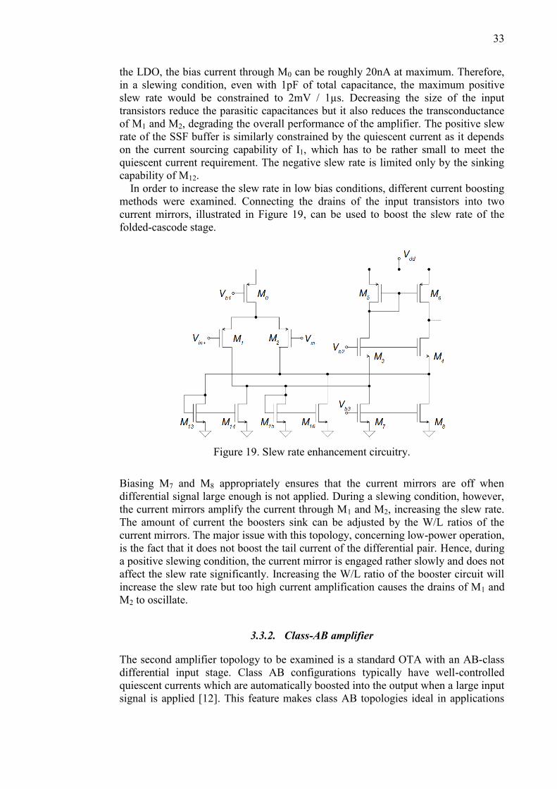
In order to increase the slew rate in low bias conditions, different current boosting
methods were examined. Connecting the drains of the input transistors into two
current mirrors, illustrated in Figure 19, can be used to boost the slew rate of the
folded-cascode stage.
Figure 19. Slew rate enhancement circuitry.
Biasing M7 and M8 appropriately ensures that the current mirrors are off when
differential signal large enough is not applied. During a slewing condition, however,
the current mirrors amplify the current through M1 and M2, increasing the slew rate.
The amount of current the boosters sink can be adjusted by the W/L ratios of the
current mirrors. The major issue with this topology, concerning low-power operation,
is the fact that it does not boost the tail current of the differential pair. Hence, during
a positive slewing condition, the current mirror is engaged rather slowly and does not
affect the slew rate significantly. Increasing the W/L ratio of the booster circuit will
increase the slew rate but too high current amplification causes the drains of M1 and
M2 to oscillate.
3.3.2. Class-AB amplifier
The second amplifier topology to be examined is a standard OTA with an AB-class
differential input stage. Class AB configurations typically have well-controlled
quiescent currents which are automatically boosted into the output when a large input
signal is applied [12]. This feature makes class AB topologies ideal in applications
34
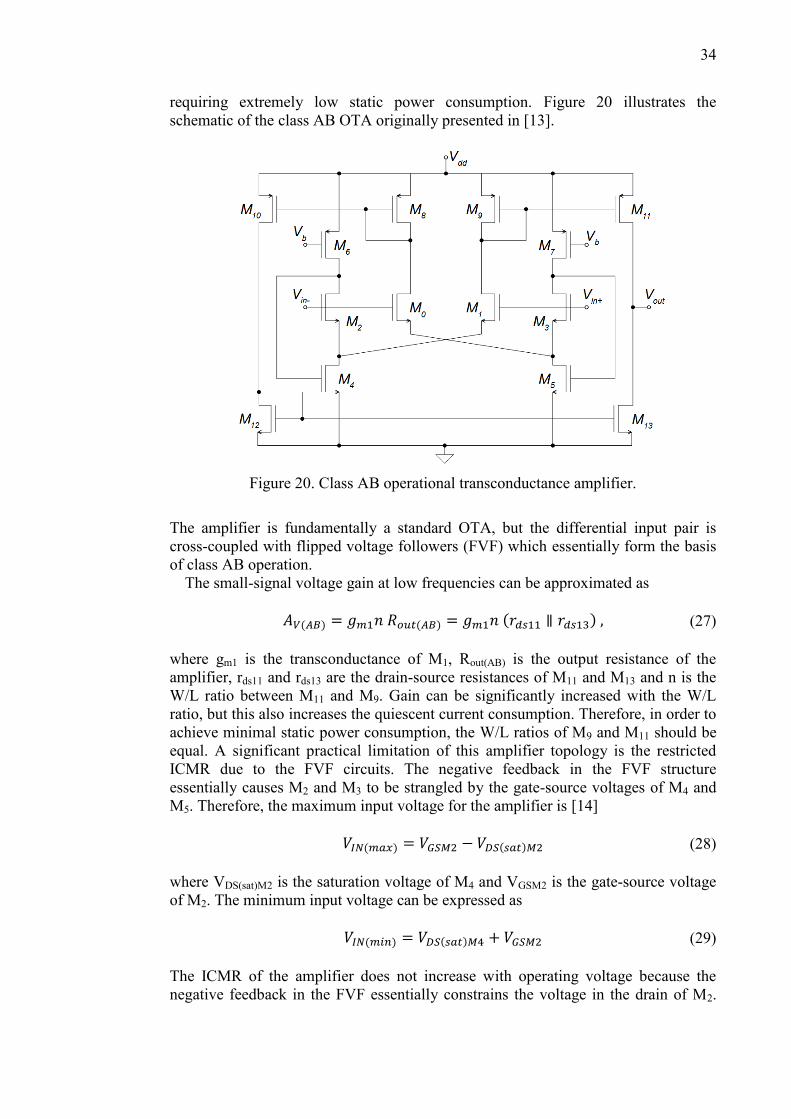
requiring extremely low static power consumption. Figure 20 illustrates the
schematic of the class AB OTA originally presented in [13].
Figure 20. Class AB operational transconductance amplifier.
The amplifier is fundamentally a standard OTA, but the differential input pair is
cross-coupled with flipped voltage followers (FVF) which essentially form the basis
of class AB operation.
The small-signal voltage gain at low frequencies can be approximated as
(27)
where gm1 is the transconductance of M1, Rout(AB) is the output resistance of the
amplifier, rds11 and rds13 are the drain-source resistances of M11 and M13 and n is the
W/L ratio between M11 and M9. Gain can be significantly increased with the W/L
ratio, but this also increases the quiescent current consumption. Therefore, in order to
achieve minimal static power consumption, the W/L ratios of M9 and M11 should be
equal. A significant practical limitation of this amplifier topology is the restricted
ICMR due to the FVF circuits. The negative feedback in the FVF structure
essentially causes M2 and M3 to be strangled by the gate-source voltages of M4 and
M5. Therefore, the maximum input voltage for the amplifier is [14]
(28)
where VDS(sat)M2 is the saturation voltage of M4 and VGSM2 is the gate-source voltage
of M2. The minimum input voltage can be expressed as
(29)
The ICMR of the amplifier does not increase with operating voltage because the
negative feedback in the FVF essentially constrains the voltage in the drain of M2.

35
Practically, input voltages only in range of 0.8 - 1.2V can be applied, which limits
the applicability of the amplifier.
The output voltage swing of the OTA is constrained by M11 dropping into the
triode region
(30)
where VDS(sat)M11 is the saturation voltage of M11. The low end of the output swing is
constrained by M13 dropping out of the active region
(31)
where VSD(sat)M13 is the saturation voltage of M13.
During a slewing condition, as a large differential input voltage is applied, the FVF
circuits force the gate-source voltages of M2 and M3 approximately constant. This
causes the gate-source voltages of M0 and M1 to change which generates current
variations with the square law. Since the sources of the differential input transistors
are cross-coupled to the FVF circuits instead to a constant current source, the
maximum output current is only restricted by the current sinking capability of M4
and M5. Therefore, the slew rate of the class AB amplifier is not constrained by the
bias current. The quiescent current can be controlled very precisely by biasing M6
and M7 accordingly. This allows the amplifier to have a high slew rate with minimal
static power consumption. [13, 14]
A severe limitation in the performance of the amplifier is the low ICMR. As the
maximum input voltage is around 1.2V, the amplifier cannot operate correctly in a
LDO configuration with a reference voltage of 1.2V. In order to improve the ICMR,
several modifications for the FVF circuit were examined. Figure 21 illustrates the
amplifier with an improved version of the FVF circuit.
Figure 21. Class AB amplifier with cascoded FVF circuits.

36
This implementation improves the ICMR range by adding PMOS cascoding
transistors M14 and M15 into the FVF feedback loop. They provide a level shift
proportional to the bias voltage Vb2. Therefore, the maximum voltage at the drain of
M2 during idle is approximately Vb2 + VSGM14, which is very close to the operating
voltage if Vb2 is set correctly. Hence, the positive ICMR range is significantly
improved.
Another modification to improve the ICMR of the FVF is illustrated in Figure 22.
In this case, a level shifter and a diode-connected transistor are added to the feedback
loop.
Figure 22. FVF ICMR improvement with level shifters.
In this configuration, the voltage at the gate of M14 is approximately VGSM4 +
VGSM16 + MGSM14 which can also be very close to the operating voltage. The level
shift achieved by M14 and M16 can be maximized by connecting the bulk nodes of the
corresponding transistors to the ground, which increases the threshold voltage.
Therefore, the voltage at the drain of M2 is higher and ICMR of the amplifier is
significantly increased. A minor drawback in this improvement is the slightly
increased quiescent current consumption as the bias current through M16 and M14 has
to be equal with the bias current through M6.
3.3.3. Comparison of error amplifiers
Table 4 summarizes the properties of the two amplifiers discussed in previous
sections.

37
Table 4. Summary of error amplifier properties
Folded-cascode OTA &
SSF Buffer
Class AB OTA with the
modified FVF
Small signal gain
Output resistance
ICMR
(max, min)
Output swing
(max, min)
Slew rate
The goal of examining quite different approaches on the error amplifier is to
illustrate the limits of traditional class A amplifiers and moreover, how adequate
performance can be achieved with class AB implementations. Obviously, as in the
case of class A amplifiers, small bias current degrades the performance of class AB
OTAs equivalently as large MOS resistances create delay with parasitic capacitances.
However, class AB amplifiers are essentially able to operate in low current
environments where conventional amplifiers cannot. Also, utilizing multiple stages
in the amplifier structure is rather impractical in this case since biasing currents of
the different stages would have to be very small resulting in low performance.
The class AB OTA also benefits from simplicity as it only requires one voltage to
precisely control the bias point whereas the folded-cascode structure itself requires
three. The simplicity of setting the bias point can be used in creating a biasing circuit
which tracks the load current of the LDO and adjusts the bias voltage accordingly.
Achieving this with the folded-cascode structure would be more complicated, since
three voltages would have to be controlled as a function of the load current.
Since the two amplifiers have rather different output impedance characteristics,
they have a large impact on the frequency response of the system. The class-AB
OTA has large output impedance for which it is most beneficial to utilize in on-chip
NMOS LDOs. Therefore the large output impedance forms the dominating pole
while the output pole is pushed to high frequencies. In the buffered folded-cascode
implementation, it is most beneficial to utilize a PMOS pass device. The high open-
loop output impedance of the PMOS can be used to make the output pole dominating
while the amplifier pole is pushed to higher frequencies due to low output impedance
of the buffer circuit.
A drawback in the class AB OTA compared to the folded-cascode, is the limited
ICMR in both directions. The low end ICMR in the folded-cascode extends below
the lower supply voltage for which it can operate with lower input voltages. This
property is beneficial if lower reference voltages, such as 0.6V, have to be used. The
class AB amplifier, however, has significantly higher low end ICMR for which lower
reference voltages cannot be used. In practice, the minimum reference voltage for the
AB OTA is 1V because headroom for variation is also needed. The high end of
ICMR is not a problem since it can be solved with the FVF improvement. The latter
of the illustrated ICMR improvements is selected because the cascoded FVF circuits
have problems operating quickly enough in low current conditions.

38
3.4. Sensing the load current
Even if the amplifier is capable of boosting the bias current to the output, its
performance is still relatively low if kept under constant bias. This can be overcome
by utilizing an adaptive biasing circuit which senses the load current and adjusts the
bias point of the amplifier correspondingly. Sensing the load current in a NMOS
LDO essentially requires a replica of the pass device with similar gate-source and
drain voltages. Figure 23 presents a circuit which senses a fraction of the load current
and also generates a bias voltage corresponding to the load current.
Figure 23. Load current sensing and adaptive biasing circuitry.
The PMOS current mirror formed by M2 and M3 replicates the output voltage to
the source of the current sensing transistor M1. The fraction of the load current
through M1 is therefore determined by the properties of the PMOS current mirror and
the ratio 1:K between M1 and the pass device. The current through M1 creates a load-
dependent voltage at the gate of M4 which is used to control the current of M5.
Therefore, when the load current is small, M5 pulls only a small amount of current
and the constant current source Ib2 determines the standby bias voltage at the gate of
M6. As the load current increases, the gate voltage of M4 increases equivalently,
causing M5 to pull more current which decreases the bias voltage. The capacitor C1
provides filtering in case the LDO supplies a digital circuit.

39
4. DESIGNING THE LDO
The LDO will be designed and simulated with a 0.6µm CMOS process, which has
isolated deep n-well NMOS transistors available. The environment for the LDO
consists of a buffered 1V reference voltage and a regulated 2.5V input voltage for the
charge pump. This section describes choices and considerations made in the design
process.
4.1. Load conditions
The regulator to be designed should have good DC regulation characteristics but the
main purpose for the LDO is the ability to supply power for digital control circuitry.
Estimated complexity for the digital load is roughly 100000 equivalent gates. For
simulation purposes the load circuit was modeled with DFFs and inverters clocked
simultaneously with a 5MHz clock. In addition, measurement data from a similar,
implemented load revealed that the maximum average current drawn by the digital
load is 1-3mA. Table 2 provides the approximated characteristics of the pulsed load
current based on the simulations and measurement data.
Table 2. Characteristics of the pulsed load current
Max. peak current 90mA
Frequency 5MHz
Rise & fall time 2ns
Pulse width 5ns
Evidently, the load current pulses are outside the bandwidth of the LDO which
implies that the filtering of the output voltage relies on the output capacitor. The
maximum allowable voltage drop from a single current pulse was defined to be 100
mV. The theoretical value for the output capacitor can be calculated using Equation
(8). Considering the load specifications in Table 2, the minimum output capacitance
should be 6.3nF, which obviously is too large to be integrated on silicon. This
implies that an external capacitor is necessary for highly dynamic pulsed loads; e.g.
if the output voltage filtering relied on an integrated 100pF capacitor, the voltage
drop due to a maximum current pulse would be intense, resulting in an undershoot
close to the ground potential. For the reasons mentioned above, two LDOs will be
designed: an integrated one for driving on-chip analog blocks utilizing a 100pF
output capacitor and an LDO with an external capacitor for driving the digital load
described in Table 2.
In order to determine the practical value for the external capacitor, the voltage
drop induced by a full range load current step was simulated with different output
capacitance values. Figure 24 illustrates the magnitude of the voltage drop with
different maximum peak current values.

40
Figure 24. The voltage drop induced by a pulsed load current step as a function of
output capacitance.
Based on the simulation results, a 7nF external capacitor will be used in order to
provide sufficient filtering when the logic load is enabled.
4.2. Design considerations for the feedback loop
4.2.1. Pass device characterization
The unregulated input voltage for the LDO is taken from a lithium-ion battery, the
nominal voltage of which is around 3.7V and the maximum is approximately 4,2V
during charging. An isolated deep n-well 5V NMOS transistor is used as the pass
device; they have maximum voltage rating of 5.5V which implies that even the
maximum input voltage described in the specifications will not harm the circuit.
The size of the pass device was determined as a trade-off between the gate
capacitance and the transconductance. Increasing the width essentially decreases the
output resistance of the LDO, pushing the output pole to higher frequencies. This,
however, also increases the gate capacitance which affects to the speed of the LDO.
Based on these observations, the pass device was characterized as a 5-finger NMOS
with total width of 2.5mm and channel length of 600nm.
4.2.2. The error amplifier
The final design utilizes the class AB OTA with the improved FVF circuits as the
error amplifier due to its superior performance in low power environments. The final
schematic of the amplifier can be found in Appendix 1.

41
The most important design parameter for the amplifier is the static power
consumption. To achieve the minimum quiescent current consumption of 100nA, the
bias current through transistors M6 and M7 should be roughly 8nA during standby.
Although such a bias point is possible without significant degeneration in slew rate,
the small current does however increase the impedance levels inside the amplifier
which essentially causes delay. To minimize this, 10fF capacitors C2 and C3 were
added into the FVF feedback loop in order to increase the speed of the amplifier in
low current conditions. The delay occurs only in the low biasing points; even a slight
increase in the quiescent current improves the dynamic performance significantly. To
illustrate this, Figure 25 presents the amplifiers’ response to a transient in a low, and
slightly higher, biasing point.
Figure 25. Amplifier transient response dependency on the bias current.
As seen in Figure 25, the slew rate is high regardless of the low bias current. The
inevitable consequence of the low bias is the delay which is approximately 2µs on
the rising edge and 3 µs on the falling edge. However, when the bias current through
M6 and M7 is slightly increased, the amplifier response improves significantly.
4.3. Adaptive biasing
The current sensing circuitry presented in Section 3.4 is used to generate a bias
voltage equivalent to the load current. Figure 26 illustrates the final design of the
adaptive biasing circuit.

42
Figure 26. The complete adaptive biasing circuit.
The extra circuitry consisting of transistors M7-M13 form a booster circuit, the
purpose of which is to quickly sink current through M6 and therefore increase the
bias of the amplifier when the actual adaptive bias circuit is unable to react fast
enough. The functionality of the booster is controlled by transistors M12 and M13.
During normal operation, the gate of M7 should be grounded by enabling en2. The
booster is activated by enabling en1 and disabling en2 which causes M7 to sink a
constant current. As en1 is disabled, the voltage at the gate of M7 discharges
gradually resulting to a soft transition to the actual bias voltage level. After the
voltage settles to a desired level, en2 opens M13, pulling the gate of M7 firmly to
ground.
The effect of the booster circuit on the reaction speed is illustrated in Figure 27
which presents how output voltage of the biasing circuit reacts to a change in the
load current.
Figure 27. Bias voltage with the booster circuit enabled (blue) or disabled (green).

43
The booster circuit not only allows the amplifier to be biased faster, but also to a
higher bias point during startup which results in improved response to the load step
in terms of undershoot and settling time.
The output voltage bias circuitry has to be limited though, as the maximum DC
output current is designed to be 100mA. If the bias voltage drops too low due to the
high load current, it will decrease the voltage levels inside the error amplifier and
eventually decreases performance. In addition, the bias point affects to the position
of the dominant pole; if the amplifier is biased too high, the position of the dominant
approaches the output pole, decreasing phase margin. Hence, the bias circuit is
adjusted so that the lowest bias voltage for the amplifier will be roughly 3.6V. The
schematic of the final adaptive biasing circuitry can be found in Appendix 2.
4.3.1. The feedback resistors
The concept of controlling the output voltage of a LDO regulator is based on
adjusting the resistance of the feedback resistor RFB1. In the circuit level
implementation, presented in Appendix 3, an array of MOS switches is used to
bypass a specific portion of RFB1, decreasing the resistance seen by the feedback
node and therefore changing the output voltage level. The value of RFB2 should be
considered carefully as it determines the minimum quiescent current through MN. As
the error amplifier consumes most of the quiescent current in the system, the
maximum biasing current through MN should be in scale of 30nA. The current
through MN during standby can be determined from
(32)
If RFB2 is set to 32MΩ and Vfb is taken from a buffered 1V source, the quiescent
current through MN is approximately 31nA which satisfies the requirement. The
output voltage is designed to be adjustable from 1.2V to 1.8V with 100mV
increments. Using Equation (1), corresponding resistance for RFB1 can be calculated
for each output voltage level. These values are illustrated in Table 3.
Table 3. Resistor values for different output voltage levels
Vout [V] RFB1 [Ω]
1.2 6.4M
1.3 9.6M
1.4 12.8M
1.5 16M
1.6 19.2M
1.7 22.4M
1.8 25.6M
The tradeoff with the small quiescent current through MN is the large time constant
created by the feedback resistors and the capacitance seen by them, which essentially
increases the settling time of the output voltage. This is problematic e.g. in case the

44
load current increases before the output has reached its nominal level, potentially
resulting in an extensive undershoot.
The issue with the long settling time can be solved by decreasing the resistances of
RFB1 and RFB2 to a fraction of their nominal values when necessary. This can be
implemented with a network of MOS switches which bypass large portions of both
RFB1 and RFB2. The complexity of the resistor network is increased though, as the
scalability is required for all possible output voltages. The principle of the circuit
level implementation is illustrated in Figure 28.
Figure 28. The concept of decreasing the resistances of RFB1 and RFB2.
RFB1 is divided into smaller fractions, e.g. each level being a tenth of the original
value specified in Table 3, which are connected into the feedback node with MOS
switches. Likewise, RFB2 is also divided into two fractions in order to keep the ratio
between the resistors correct. The input bits v[n-1:0] are used control the output
voltage selection while the input s[0:1] controls whether the higher or lower resistors
are selected. To maintain correct ratio between RFB1 and RFB2, v[n] is used to bypass
the required portion of RFB2.
The final resistance values for the secondary feedback resistors are presented in
Table 4. Most of the resistances are 10% of the values presented in Table 3. For the
lowest output voltages, however, the resistances are 25% of their original values. To
maintain the feedback ratio, 8MΩ segment is split from RFB2. The reason for this is
the compensation of the LDO and will be explained in the following Section. The
schematic of the complete feedback resistor network can be found in Appendix 3.
Table 4. Values for the decreased feedback resistors.
Vout [V] RFB1 [Ω] RFB2 [Ω]
1.2 1.6M 8M
1.3 2.4M 8M
1.4 3.2M 8M
1.5 1.6M 3.2M
1.6 1.92M 3.2M
1.7 2.24M 3.2M
1.8 2.56M 3.2M

45
Switching between the two operational modes can be done by monitoring the load
current; as the load increases to a specific point, the s[1:0] bits are used to connect
the smaller resistors to the feedback node while disconnecting the higher ones. This
functionality can be can be implemented on-chip since the information on the
magnitude of the load current is in the adaptive biasing circuit presented in Section
3.4. Figure 29 illustrates a simple comparator attached into the adaptive biasing
circuitry which can be used to control the resistor network.
Figure 29. Comparator added into the adaptive biasing circuit.
This affects the quiescent current consumption relatively little as the currents in the
biasing circuit are quite low in the standby mode. Because of this the reference
current Ic only has to be a few nanoamperes.
4.4. Compensation
The basic idea of frequency compensation is to modify the transfer function of the
LDO in a way that stability and good settling characteristics are achieved regardless
of operating conditions, temperature or different process corners. The load
environment of the LDO to be designed is diverse, ranging roughly from 10nA to
maximum of 100mA of DC current. Such a wide range of possible load currents
causes the location of the output pole to move extensively, which complicates the
compensation.
During high loads the two major poles are split widely, especially in case the
regulator only has the internal capacitor. As the LDO is powered down into standby
and the load current decreases below 1µA, the output pole is pulled closer to the
dominant pole, decreasing phase margin significantly. In fact, in case the LDO
utilizes the external 7nF capacitor, the location of the output pole will almost be on
the same frequency as the dominant pole when the load current is low enough.
Splitting the poles sufficiently during the standby state is difficult since it would
require a large capacitance in the output of the error amplifier to pull the dominant
pole at least a decade below the output pole. In addition, a switching system would

46
be needed to detach the capacitor from the circuit during high loads to prevent loss of
performance. A more effective approach in this case is to create a zero to cancel the
output pole throughout its movement range.
Figure 30 illustrates two methods of creating a zero to compensate for the output
pole movement.
a) b)
Figure 30. LDO compensation methodologies with a) a series RC network to ground
or b) a series RC network to the feedback node.
In Figure 30 a), a series RC network is added into the output node of the error
amplifier. It essentially creates a zero on a frequency
(33)
where Cc and Rc are the capacitance and resistance in the compensation network.
This compensation network is quite effective if the zero can be made to track the
output pole, hence canceling the output pole throughout its movement range.
Therefore, the resistance of Rc should be adjusted as a function of the load current.
This can be achieved by utilizing the adaptive biasing circuitry presented in Section
3.4. As the voltage on the gates of M4 and M5 in Figure 23 is dependent on the load
current, it can be used to change the drain-source resistance of a NMOS transistor.
Thus, a zero which tracks the output pole can be created by replacing Rc in Figure 30
a) with a NMOS transistor controlled by the adaptive biasing circuit. The adaptive
biasing circuitry, however, is unable to provide the NMOS low bias voltage enough
to provide compensation during low loads. Hence in this system, the compensation
system is effective only on medium to high loads. Figure 30 b) illustrates another
method for creating a zero which tracks the load current. Similarly as in the previous
implementation, the adaptive biasing circuit can be used to adjust the resistance of
Rc. In this case, however, the compensation capacitor also sees other resistances in
the feedback node which are large due to the quiescent current requirement. The
frequency on which the zero is formed can be approximated as
(34)
This implies that even though Rc is adjusted, the location of the zero is constrained
by the parallel combination of RFB1 and RFB2. For this, in order for the compensation
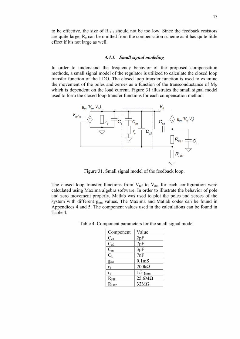
47
to be effective, the size of RFB1 should not be too low. Since the feedback resistors
are quite large, Rc can be omitted from the compensation scheme as it has quite little
effect if it's not large as well.
4.4.1. Small signal modeling
In order to understand the frequency behavior of the proposed compensation
methods, a small signal model of the regulator is utilized to calculate the closed loop
transfer function of the LDO. The closed loop transfer function is used to examine
the movement of the poles and zeroes as a function of the transconductance of MN
which is dependent on the load current. Figure 31 illustrates the small signal model
used to form the closed loop transfer functions for each compensation method.
Figure 31. Small signal model of the feedback loop.
The closed loop transfer functions from Vref to Vout for each configuration were
calculated using Maxima algebra software. In order to illustrate the behavior of pole
and zero movement properly, Matlab was used to plot the poles and zeroes of the
system with different gmn values. The Maxima and Matlab codes can be found in
Appendices 4 and 5. The component values used in the calculations can be found in
Table 4.
Table 4. Component parameters for the small signal model
Component Value
Cc1 2pF
Cc2 7pF
Cgs 3pF
CL 7nF
gm1 0.1mS
r1 200kΩ
rc 1/3 gmn
RFB1 25.6MΩ
RFB2 32MΩ

48
The pole and zero behavior in the uncompensated case are illustrated in Figure 32,
in which the arrows visualize the movement of the complex poles and zeroes as gmn
increases.
Figure 32. Uncompensated LDO pole and zero movement.
The nature of the poles and zeroes is heavily dependent on the load current, as
illustrated in Figure 32. When the transconductance of MN is low, the system has
complex zero and pole pairs and also one real pole. It is quite obvious that the LDO
has low phase margin at low loads as the poles are close to the imaginary axis and
this results in significant resonance peaking at the specific frequency. As the load
current increases, the poles eventually move onto the real axis. The zeroes in the
system also have a similar nature; they are complex on low loads but move to the
real axis as the load increases. The analysis confirms the severity of the frequency
behavior on low loads which imposes severe requirements for the compensation
methods.
The frequency behavior of the compensation method in Figure 30 a) is presented
in Figure 33. The poles and zeroes in the system are in this case real, and it can be
seen that the location of the zero tracks the pole. As the model is ideal, the zero
tracks the pole on a wide range of frequencies. In practice, however, the resistance of
the transistor used as Rc cannot be large enough to pull the zero to very low
frequencies.

49
Figure 33. Pole and zero movement in the first compensation scheme.
Figure 34 illustrates the zero-pole behavior of the LDO utilizing the compensation
method presented in Figure 30 b) with Rc omitted. In this case, the system has a
complex pole pair, one real pole and real zeroes. When gmn is low, the complex poles
still have relatively high Q-factors but this property decreases quite rapidly as gmn
increases. Eventually the poles shift on the real axis and they move to the left along
the real axis on the zero-pole map.
Figure 34. Pole and zero movement in the second compensation scheme.

50
4.4.2. Proposed compensation scheme
The final compensation scheme utilizes both of the previously presented
compensation methods. The capacitor between the feedback node and the gate of the
pass device compensates the LDO on low frequencies while the adaptive
compensation network creates a zero which tracks the output pole on higher
frequencies. Figure 35 illustrates the principle of the proposed compensation method.
Figure 35. Implementation of the proposed compensation method.
The two compensation methods do not interfere with each other as the capacitor Cz
affects the frequency response only on low loads and the series RC network
compensates the LDO only on higher loads. The capacitor Cz is beneficial also for
creating a faster feedback path, therefore improving the dynamic characteristics.
This compensation method is used in both of the LDO designs, the difference
between the two is the size of the compensation capacitor between the feedback node
and the gate of the pass device. In the fully integrated implementation, the output
pole stays on higher frequencies even on low loads. The compensation capacitor Cz
in this case is 3pF. The LDO with the external capacitor requires much heavier
compensation, for which the value of Cz in this case is 7pF. Both of the LDOs have
quite similar frequency characteristics on high loads; therefore Cc is 2pF for both
implementations. A zero-pole map of the proposed compensation scheme for the
LDO with the external capacitor is illustrated in Figure 36. It can be seen that the
trail of the complex poles has flattened and their Q-factors decrease faster.

51
Figure 36. Pole and zero behavior of the proposed compensation method with the
external output capacitor.
4.5. The charge pump
The primary requirement for the charge pump is the ability to supply a sufficient
amount of current, because the operational amplifier requires large amounts of
current during heavy transients. To ensure that the output voltage of the charge pump
will not undershoot too low, it should be able to supply roughly 50µA of current. The
output resistance should be kept as low as possible to minimize the voltage drop
when current is drawn from the charge pump. To minimize the output resistance, the
circuit will utilize two phases; this configuration essentially halves the output
resistance and also allows smaller capacitors to be used. The circuit is clocked with
non-overlapping, 10MHz clock signals. Figure 37 illustrates the startup of the charge
pump after it is enabled.
Figure 37. Charge pump startup.

52
After the charge pump has been enabled, the unloaded output voltage increases to the
maximum value of 4.2V in approximately 5µs. The schematic of the charge pump
can be found in Appendix 6.
4.6. The final LDO model
The top level schematic of the circuit elements in the LDO is presented in Figure 38.
All components, including the passive ones, were modeled using components from
the 0.6µm CMOS process.
Figure 38. Top level schematic of the designed LDO.
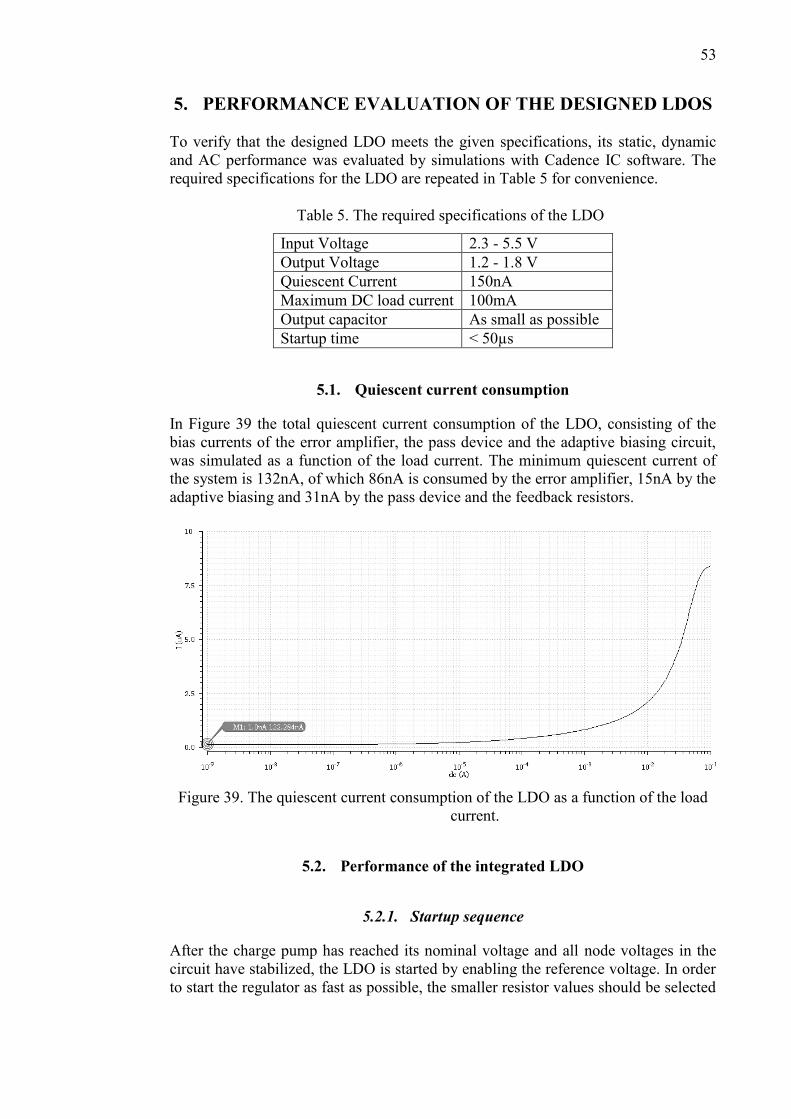
53
5. PERFORMANCE EVALUATION OF THE DESIGNED LDOS
To verify that the designed LDO meets the given specifications, its static, dynamic
and AC performance was evaluated by simulations with Cadence IC software. The
required specifications for the LDO are repeated in Table 5 for convenience.
Table 5. The required specifications of the LDO
Input Voltage 2.3 - 5.5 V
Output Voltage 1.2 - 1.8 V
Quiescent Current 150nA
Maximum DC load current 100mA
Output capacitor As small as possible
Startup time < 50µs
5.1. Quiescent current consumption
In Figure 39 the total quiescent current consumption of the LDO, consisting of the
bias currents of the error amplifier, the pass device and the adaptive biasing circuit,
was simulated as a function of the load current. The minimum quiescent current of
the system is 132nA, of which 86nA is consumed by the error amplifier, 15nA by the
adaptive biasing and 31nA by the pass device and the feedback resistors.
Figure 39. The quiescent current consumption of the LDO as a function of the load
current.
5.2. Performance of the integrated LDO
5.2.1. Startup sequence
After the charge pump has reached its nominal voltage and all node voltages in the
circuit have stabilized, the LDO is started by enabling the reference voltage. In order
to start the regulator as fast as possible, the smaller resistor values should be selected

54
during the startup. Also, enabling the booster in the adaptive biasing circuit
simultaneously with the reference voltage allows the LDO to settle faster and more
precisely to the correct output voltage level. Figure 40 illustrates the startup process,
where the charge pump has been enabled 20µs before the reference voltage. It can be
seen that the output voltage is on its nominal level in approximately 30µs after the
reference has been enabled.
Figure 40. Output voltage after the reference has been enabled.
5.2.2. Output voltage accuracy
The output voltage accuracy of the LDO was tested against variations in input
voltage, the ambient temperature and the effects of different process corners. The
output voltage was set to 1.8V while the input voltage was swept from 2.3V to 5.5V.
Accuracy against temperature variation was tested in two extreme ends, in -40°C and
in 125°C. It was found that the nominal output voltage throughout the input voltage
range was 1.804V. The largest deviation from the nominal output level was 2.4mV
which occurred in the slow process corner. The voltage accuracy was also tested in
the lower end of the output voltage range. When the output voltage was set to the
1.2V level, it was found that nominal voltage in the output was 1.2025V. The largest
deviation from the nominal level was measured as 1.3mV, which also occurred in the
slow process corner. These results do not include random offsets.
5.2.3. Power supply rejection
As the error amplifier has its own power supply, the power supply rejection
corresponds to the isolation between the drain and source of the pass transistor. The
PSR was simulated in the extreme ends of the input voltage and the load current
range. Also, since the state of the feedback resistors has an effect on the
performance, both cases were simulated for the full load range. Figures 41 and 42

55
present the PSR response with the lower feedback resistors enabled on 100nA and
100mA load currents.
Figure 41. LDO PSR response at 1.2V.
Figure 42. LDO PSR response at 1.8V.
As seen in Figure 41, the PSR response at 1.2V output voltage is quite unitary
between the high and low load. In Figure 42, however, this difference between the
PSR curves is approximately 15dB. The degradation of PSR on the high load current
occurs because the gate-source voltage of the pass device increases which causes the
transistor to shift closer to the triode region, where the PSR essentially decreases.
This does not occur on lower output voltages as the pass device stays in the active
region. Figures 43 and 44 illustrate the PSR in similar cases as before, but with the
higher feedback resistance values enabled instead.

56
Figure 43. PSR response at 1.2V with the higher feedback resistors enabled.
Figure 44. PSR response at 1.8V with the higher feedback resistors enabled.
In this case the PSR is more consistent at 1.8V level while on 1.2V output level the
difference between high and low load is 13dB. The PSR in the 1.8V case is more
consistent than in Figure 42. The reason for this is the smaller bias current through
the pass device for which the gate-source voltage doesn’t need to be as high, keeping
the transistor in the active region.
The effect of process variations on the overall PRS is rather small. The largest
deviation from the typical level was 2dB. Table 6 summarizes the typical PSR values
of the LDO at 1kHz frequency.
Table 6. LDO PSR in the typical process corner at 1kHz
Iload RFB state Vout = 1.2V Vout = 1.8V
100nA High 45dB 40dB
100nA Low 44dB 35dB
100mA High 58dB 36dB
100mA Low 47dB 19dB
5.2.4. Frequency behavior
The frequency behavior of the LDO was simulated to verify that the LDO is stable
and has sufficiently phase margin in all operating conditions. Figure 45 illustrates the

57
simulated open loop frequency response at 1.8V output voltage. It can be seen that
on a high load, the state of the feedback resistors has a relatively insignificant effect
on the loop gain. On low loads, however, the zero is pulled to lower frequencies and
GBW is extended. The GBW of the LDO on a full load is roughly 2MHz while on a
low load current it is reduced to 10kHz. When the higher feedback resistors are
enabled, the GBW during a low load is extended to 40kHz. In order to verify
sufficient phase margin in all possible operation conditions, the stability analysis was
performed for all available output voltages throughout the load current range. Figure
46 illustrates a contour map of how the phase margin behaves on different output
voltages and load currents when the lower feedback resistors are enabled. Figure 47
presents the results of the phase margin simulation with the higher feedback resistors
enabled.
Figure 45. Open loop gain and phase responses on high and low load current.
Figure 46. Contour map of phase margin as a function of output voltage and load
current with low feedback resistors enabled.

58
Figure 47. Contour map of phase margin as a function of output voltage and load
current with the large feedback resistors enabled.
The simulation results verify that the phase margin of the integrated LDO does not
drop under 40 degrees in any operating condition. In Figure 46, the phase margin is
at its minimum when the input voltage and the output current are at their minimum
since the output pole falls to lower frequencies than the compensating zero. As the
adaptive compensation becomes effective, the zero cancels the output pole quite
consistently throughout the frequency range. In Figure 47, the low phase margin
during low load currents is essentially improved as the higher output resistors pull
the compensating zero on lower frequencies.
5.2.5. Transient performance
The dynamic characteristics of the LDO were tested to ensure that the output voltage
stays within acceptable levels during line and load transients. The line transient
response was simulated by injecting a voltage change with a slope of 1V/20µs to the
input line. Figure 48 illustrates the output voltage variation due to the line transient.
The output variation induced by the rising edge of the line transient was determined
to be 12.6mV while the falling edge caused a 15mV fluctuation. The increase in the
variation in different process corners was approximately 1mV to both directions.
Based on the form of the output fluctuation one can see that the nature of the signal
feed-through is capacitive.
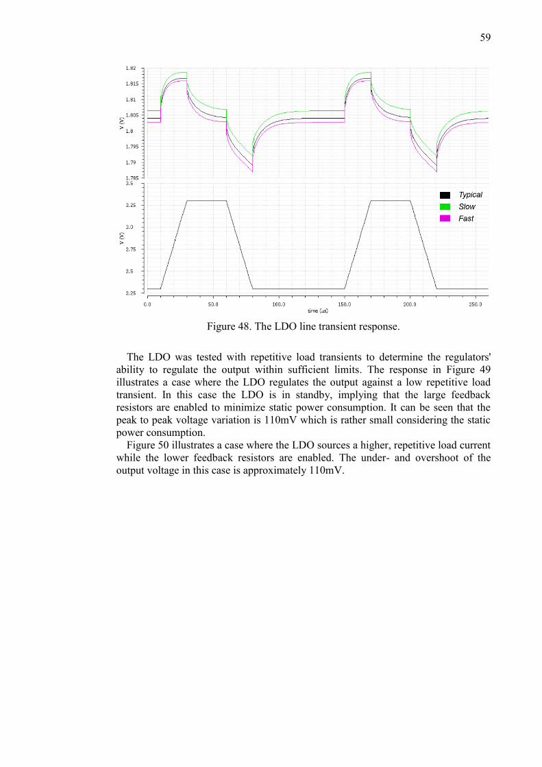
59
Figure 48. The LDO line transient response.
The LDO was tested with repetitive load transients to determine the regulators'
ability to regulate the output within sufficient limits. The response in Figure 49
illustrates a case where the LDO regulates the output against a low repetitive load
transient. In this case the LDO is in standby, implying that the large feedback
resistors are enabled to minimize static power consumption. It can be seen that the
peak to peak voltage variation is 110mV which is rather small considering the static
power consumption.
Figure 50 illustrates a case where the LDO sources a higher, repetitive load current
while the lower feedback resistors are enabled. The under- and overshoot of the
output voltage in this case is approximately 110mV.

60
Figure 49. LDO response for a repetitive low load transient.
Figure 50. LDO response for a repetitive intermediate load transient.

61
Figure 51 illustrates a more practical transient simulation where the load current is
sequentially stepped up and down e.g. operational amplifiers being powered on and
off. It can be seen quite clearly that as the load current increases, also the regulation
performance of the LDO improves. Based on the transient simulations, it can be said
that process variations have quite an insignificant effect on regulation performance.
Figure 51. Transient response in case of a practical load.
5.2.6. Noise
The simulated output noise on 100nA and 100mA loads is presented in Figure 52. It
can be seen that 1/f-noise of the MOS transistors dominates on low frequencies. As
the 1/f-noise is dependent on the transconductance, it can be seen that the 1/f-noise
curve becomes more gradual as load current increases.
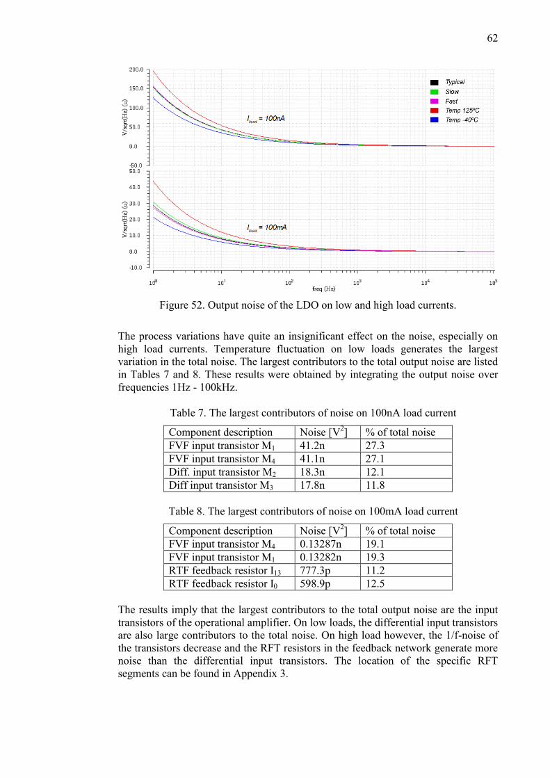
62
Figure 52. Output noise of the LDO on low and high load currents.
The process variations have quite an insignificant effect on the noise, especially on
high load currents. Temperature fluctuation on low loads generates the largest
variation in the total noise. The largest contributors to the total output noise are listed
in Tables 7 and 8. These results were obtained by integrating the output noise over
frequencies 1Hz - 100kHz.
Table 7. The largest contributors of noise on 100nA load current
Component description Noise [V2] % of total noise
FVF input transistor M1 41.2n 27.3
FVF input transistor M4 41.1n 27.1
Diff. input transistor M2 18.3n 12.1
Diff input transistor M3 17.8n 11.8
Table 8. The largest contributors of noise on 100mA load current
Component description Noise [V2] % of total noise
FVF input transistor M4 0.13287n 19.1
FVF input transistor M1 0.13282n 19.3
RTF feedback resistor I13 777.3p 11.2
RTF feedback resistor I0 598.9p 12.5
The results imply that the largest contributors to the total output noise are the input
transistors of the operational amplifier. On low loads, the differential input transistors
are also large contributors to the total noise. On high load however, the 1/f-noise of
the transistors decrease and the RFT resistors in the feedback network generate more
noise than the differential input transistors. The location of the specific RFT
segments can be found in Appendix 3.
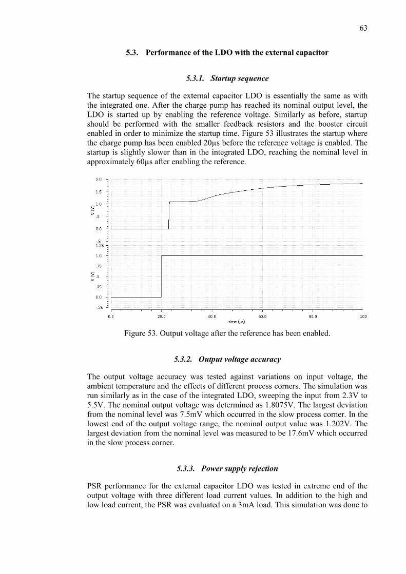
63
5.3. Performance of the LDO with the external capacitor
5.3.1. Startup sequence
The startup sequence of the external capacitor LDO is essentially the same as with
the integrated one. After the charge pump has reached its nominal output level, the
LDO is started up by enabling the reference voltage. Similarly as before, startup
should be performed with the smaller feedback resistors and the booster circuit
enabled in order to minimize the startup time. Figure 53 illustrates the startup where
the charge pump has been enabled 20µs before the reference voltage is enabled. The
startup is slightly slower than in the integrated LDO, reaching the nominal level in
approximately 60µs after enabling the reference.
Figure 53. Output voltage after the reference has been enabled.
5.3.2. Output voltage accuracy
The output voltage accuracy was tested against variations on input voltage, the
ambient temperature and the effects of different process corners. The simulation was
run similarly as in the case of the integrated LDO, sweeping the input from 2.3V to
5.5V. The nominal output voltage was determined as 1.8075V. The largest deviation
from the nominal level was 7.5mV which occurred in the slow process corner. In the
lowest end of the output voltage range, the nominal output value was 1.202V. The
largest deviation from the nominal level was measured to be 17.6mV which occurred
in the slow process corner.
5.3.3. Power supply rejection
PSR performance for the external capacitor LDO was tested in extreme end of the
output voltage with three different load current values. In addition to the high and
low load current, the PSR was evaluated on a 3mA load. This simulation was done to
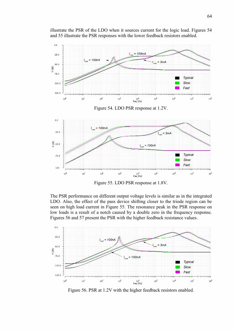
64
illustrate the PSR of the LDO when it sources current for the logic load. Figures 54
and 55 illustrate the PSR responses with the lower feedback resistors enabled.
Figure 54. LDO PSR response at 1.2V.
Figure 55. LDO PSR response at 1.8V.
The PSR performance on different output voltage levels is similar as in the integrated
LDO. Also, the effect of the pass device shifting closer to the triode region can be
seen on high load current in Figure 55. The resonance peak in the PSR response on
low loads is a result of a notch caused by a double zero in the frequency response.
Figures 56 and 57 present the PSR with the higher feedback resistance values.
Figure 56. PSR at 1.2V with the higher feedback resistors enabled.

65
Figure 57. PSR at 1.8V with the higher feedback resistors enabled.
It can be seen that PSR in case of 1.2V output voltage is quite similar as in figure 54.
The PSR at 1.8V on 100mA load, however, is improved. This occurs because the
gate-source voltage of the pass device doesn't need to be as large to source the
current due to the lower bias point. Table 9 presents the typical PSR values of the
LDO at 1kHz frequency. The peak in the PSR response on low load current occurs
close to the frequency on which the PSR values were measured, explaining the
degraded attenuation on low loads.
Table 9. LDO PSR in the typical process corner at 1kHz
Iload RFB state Vout = 1.2V Vout = 1.8V
100nA High 30dB 25dB
100nA Low 52dB 53dB
3mA High 57dB 49dB
3mA Low 50dB 36dB
100mA High 51dB 30dB
100mA Low 40dB 15dB
5.3.4. Frequency behavior
Stability of the LDO was tested by simulating the open-loop frequency response. In
Figure 58, open-loop gain and phase responses are shown, simulated with the load
current values 100nA and 100mA while the output voltage was set to 1.8V. The
effect of the large output capacitor can be seen clearly on low currents as the output
pole is pulled within a decade of the dominant pole. The compensation capacitor
between the gate of the pass device and the feedback node essentially creates the
zero pair which causes the notch in the loop gain. It can be seen that the phase
margin of the system drops quite low in case the larger feedback resistors are not
enabled. The GBW in this case is slightly above 2MHz when the load current is
100mA while on the low load, the GBW is reduced to 1kHz. Enabling the higher
feedback resistors extend the GBW to roughly 40kHz.

66
Figure 58. Open loop gain and phase responses on high and low current.
To verify that the LDO is stable in all operating conditions, the phase margin was
simulated against load current range and all possible output voltage levels. Figure 59
illustrates the phase margin of the system when the lower feedback resistors are
enabled. It can be seen that the phase margin drops under 15 degrees on low loads as
the feedback resistors are too small to pull the zero to sufficiently low frequencies.
The phase margin is however quite consistent when the load current increases over
4µA. Figure 60 illustrates the phase margin of the system when the higher feedback
resistors are enabled. It can be seen that phase margin on low load currents is
improved significantly. On the lower end of the output voltage range, however, the
phase margin drops close to 20 degrees.
Figure 59. Contour map of the phase margin as a function of load current and output
voltage with low feedback resistors enabled.

67
Figure 60. Contour map of the phase margin as a function of load current and output
voltage with the large feedback resistors enabled.
5.3.5. Transient performance
The dynamic performance of the LDO was simulated similarly as before with the
integrated LDO. Figure 61 illustrates the variation in the output due to a line transient
with a slope of 1V/20µs. It was found that the fluctuation in the output induced by
the rising edge of the line transient was 14.5mV while the falling edge caused a
15.6mV variation. The largest increase of the output variation in different process
corner was 1.1mV.
Figure 61. Line transient response of the LDO.
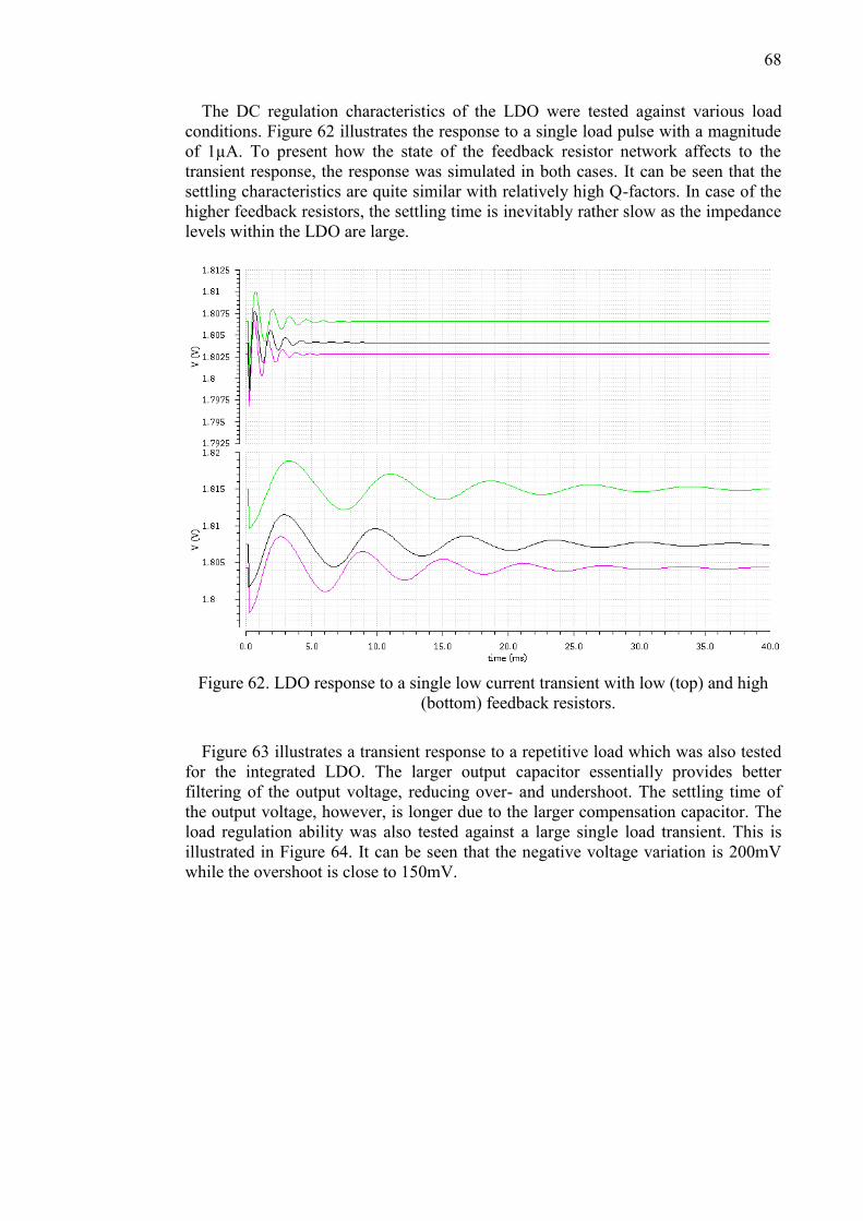
68
The DC regulation characteristics of the LDO were tested against various load
conditions. Figure 62 illustrates the response to a single load pulse with a magnitude
of 1µA. To present how the state of the feedback resistor network affects to the
transient response, the response was simulated in both cases. It can be seen that the
settling characteristics are quite similar with relatively high Q-factors. In case of the
higher feedback resistors, the settling time is inevitably rather slow as the impedance
levels within the LDO are large.
Figure 62. LDO response to a single low current transient with low (top) and high
(bottom) feedback resistors.
Figure 63 illustrates a transient response to a repetitive load which was also tested
for the integrated LDO. The larger output capacitor essentially provides better
filtering of the output voltage, reducing over- and undershoot. The settling time of
the output voltage, however, is longer due to the larger compensation capacitor. The
load regulation ability was also tested against a large single load transient. This is
illustrated in Figure 64. It can be seen that the negative voltage variation is 200mV
while the overshoot is close to 150mV.

69
Figure 63. LDO response for a intermediate repetitive load transient.
Figure 64. LDO response for a high single load current step.
In addition to the DC regulation simulations, the load transient response was tested
against a high-frequency pulsed logic load. In the first case, the LDO was set to
supply a pulsed current with the maximum amplitude while the output voltage level
was 1.8V. Figure 65 illustrates how the LDO responds when the logic load is
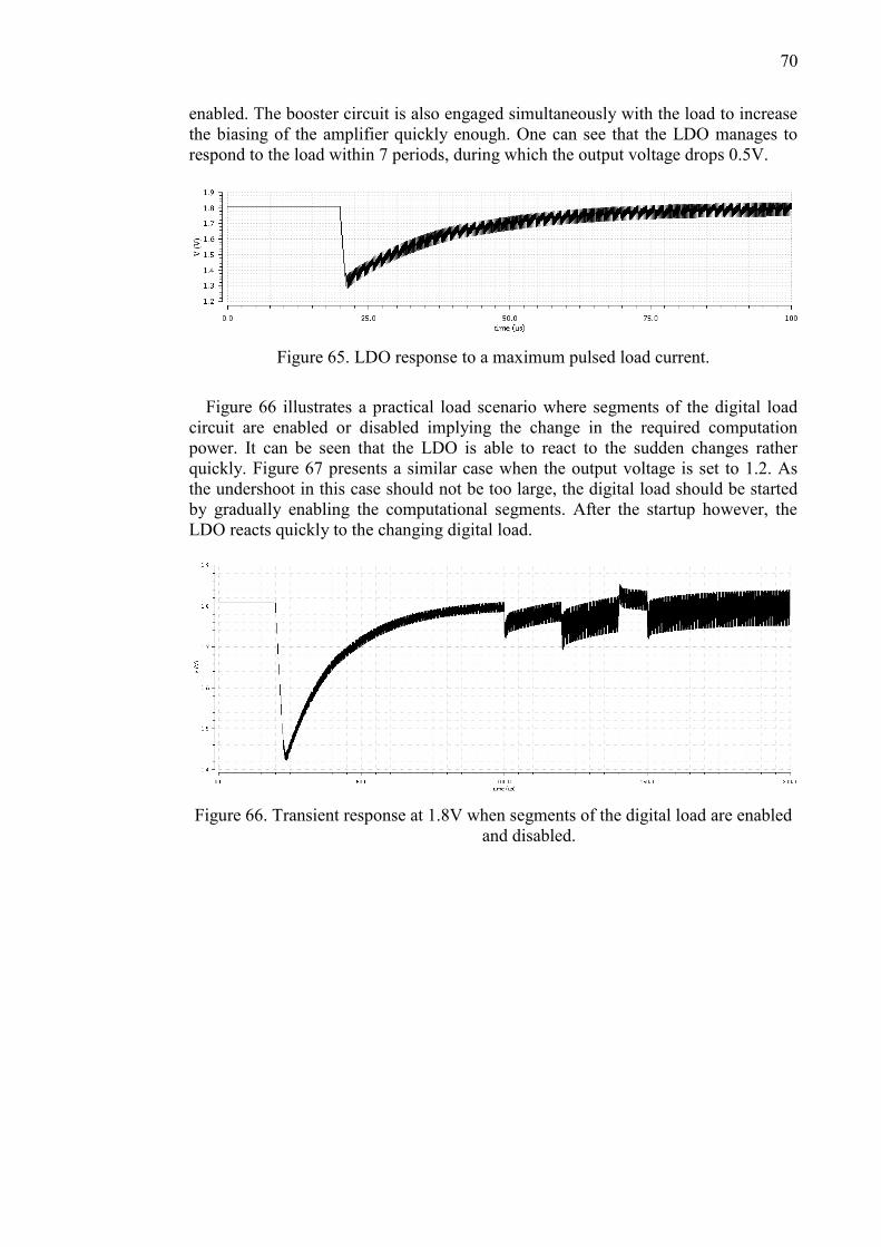
70
enabled. The booster circuit is also engaged simultaneously with the load to increase
the biasing of the amplifier quickly enough. One can see that the LDO manages to
respond to the load within 7 periods, during which the output voltage drops 0.5V.
Figure 65. LDO response to a maximum pulsed load current.
Figure 66 illustrates a practical load scenario where segments of the digital load
circuit are enabled or disabled implying the change in the required computation
power. It can be seen that the LDO is able to react to the sudden changes rather
quickly. Figure 67 presents a similar case when the output voltage is set to 1.2. As
the undershoot in this case should not be too large, the digital load should be started
by gradually enabling the computational segments. After the startup however, the
LDO reacts quickly to the changing digital load.
Figure 66. Transient response at 1.8V when segments of the digital load are enabled
and disabled.
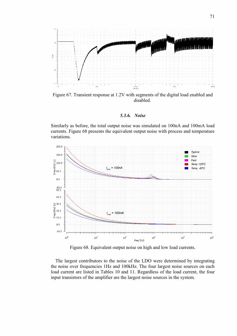
71
Figure 67. Transient response at 1.2V with segments of the digital load enabled and
disabled.
5.3.6. Noise
Similarly as before, the total output noise was simulated on 100nA and 100mA load
currents. Figure 68 presents the equivalent output noise with process and temperature
variations.
Figure 68. Equivalent output noise on high and low load currents.
The largest contributors to the noise of the LDO were determined by integrating
the noise over frequencies 1Hz and 100kHz. The four largest noise sources on each
load current are listed in Tables 10 and 11. Regardless of the load current, the four
input transistors of the amplifier are the largest noise sources in the system.
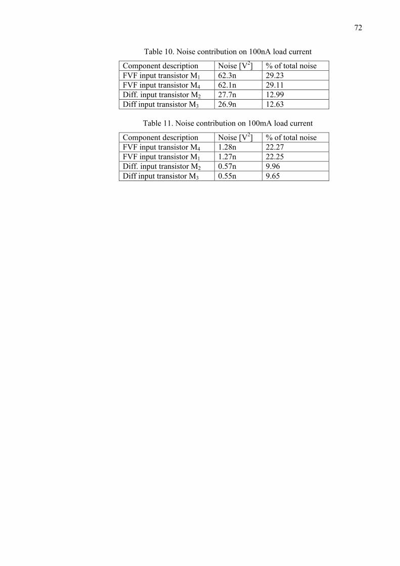
72
Table 10. Noise contribution on 100nA load current
Component description Noise [V2] % of total noise
FVF input transistor M1 62.3n 29.23
FVF input transistor M4 62.1n 29.11
Diff. input transistor M2 27.7n 12.99
Diff input transistor M3 26.9n 12.63
Table 11. Noise contribution on 100mA load current
Component description Noise [V2] % of total noise
FVF input transistor M4 1.28n 22.27
FVF input transistor M1 1.27n 22.25
Diff. input transistor M2 0.57n 9.96
Diff input transistor M3 0.55n 9.65

73
6. DISCUSSION
This thesis concentrated on studying circuit topologies applicable for a low-power,
integrated NMOS LDO regulator. Analyzing the selected topologies along with
research from the literature indicated that a class AB OTA presented in [13] was the
most suitable to be used as the error amplifier due to its superior performance in a
low current environment. The specified ability to regulate the output against a high
frequency pulsed load proved to require at least a 7nF external capacitor. As a result
of this, two separate LDOs were designed, one with the external capacitor and the
other with an integrated capacitor.
The strict requirement for the quiescent current while maintaining high speed
proved to be problematic since all design choices made to decrease the quiescent
current essentially degraded the dynamic performance. Therefore in order to have
high performance regardless of the quiescent current requirement, the LDO design
shifted towards a switched implementation. This results from the fact that the
feedback resistors determine the bias current through the pass device. Large
resistances eventually cause RC time constants with the capacitances they see which
results in slower settling time in the output. To solve this, a separate operation mode
was created by bypassing a large portion of the feedback resistors. While this
increases the complexity of the system, it also allows higher dynamic performance
with a relatively small cost. As the amplifier is the most significant part of the
feedback loop, it should be capable of high performance on low bias currents. Based
on the comparison between the amplifiers, it was found that class AB
implementations are able to provide high performance while consuming little
quiescent current.
Compensation of the LDO proved to be one the most challenging task in the
design process as the single-stage amplifier design prevented the utilization of
several compensation methods discussed in the literature. Studying the requirements
for the compensation revealed that an adaptive compensation method is necessary to
maintain high phase margin in all operating conditions. However, the drain-source
resistance of a MOS transistor cannot swing on a range wide enough to create an
adaptive zero throughout the entire load current range. This necessitated the use of a
second compensation method to create a zero at lower frequencies. It was found that
the most practical approach to creating such a zero was to add a capacitor between
the feedback node and the gate of the pass device. In case of the integrated LDO,
relatively low capacitance values could be used in both compensation networks in
order to maintain sufficient phase margin. With the external capacitor the LDO
proved to be more complicated to compensate as the large capacitor pulled the output
pole within a decade from the dominant pole. For this case, several different
compensation methods were studied to achieve an effective compensation. The most
practical solution proved to be same compensation method which was used in the
fully integrated implementation. In order to create a zero at low enough frequency
with the 7nF output capacitor, the compensation capacitor had to be increased to 7pF.
If a larger filtering capacitor is used, the phase margin will degrade even further on
low loads and the compensation should be modified in order to maintain it.
Another challenge in the design process was the relaxation oscillation problem
encountered in the class AB OTA. As the amplifier was operated on low bias
currents, it was found that as node voltages drifted from their respective levels during
large transients, they would then return quite gradually back to their nominal levels

74
due to the low bias current. Consequently, several transistors were turned off and the
amplifier was unable to respond to the load change. The problem was essentially
solved by modifying the FVF circuits in the amplifier. Detecting this phenomenon,
however, proved to be tricky since the behavior of the node voltages could only be
inspected with transient analysis.
Sourcing a large DC current while operating under a 0.5V dropout voltage proved
to shift the pass device to the triode region which caused degradation e.g. in the PSR
response on high loads. This is essentially a weakness in the NMOS topology; if low
dropout voltage is required, the voltage at the gate has to be high even during
standby. In order to source high currents, the gate-source voltage has to increase
which in turn shifts the transistor towards the triode region. This occurs only on the
higher output voltages because the drain-source voltage begins to strangle the pass
device. Although the simulations were performed in the low-dropout configuration,
the intended application for this LDO uses a lithium-ion battery as the input voltage.
Therefore, the problem is essentially solved as the minimum drain voltage would be
approximately 3.7V. If the low-dropout configuration is used, this problem can also
be reduced by increasing the size of the feedback resistors which essentially
decreases the bias of the pass device, reducing the needed gate-source voltage fully
open the transistor.
Albeit the few drawbacks, both regulator designs met the required specifications.
Especially the performance of the fully integrated implementation proved to be high
considering the low static power consumption. The LDO with the external capacitor
also proved that a regulator can essentially be used to power a digital load while
maintaining good DC regulation characteristics. Due to the properties of the
amplifier, the LDO is relatively well scalable for various applications. The same
design can be used to create a high performance LDO by increasing the bias.
Further improvements to the LDO could be made by modifying the adaptive
biasing circuit to react faster to the load changes. In addition, the rate by which the
bias current increases on lower loads is relatively gradual. If the bias current
increased with a slightly steeper slope, the amplifier performance on lower loads
would increase. Improvements could also be made in compensation of the LDO. If
the resistance of a MOS transistor could swing on a wider range, the LDO could be
compensated entirely only with a RC network on the gate of the pass device.
Therefore the secondary compensation capacitor would be redundant. This would
result in significant increase in performance as the capacitance the feedback resistors
see would be considerably smaller.
The transient response characteristics of low-power LDO regulators are commonly
evaluated with a figure of merit (FOM), defined as
(35)
where TS is the settling time of the output voltage. There are, however, contradictions
in how the FOM is interpreted. In [10] and [15], TS is considered as the reaction
time whereas in [13] and [16] it is the settling time of the output voltage. In addition,
majority of the LDO designs in various publications are based on linear error
amplifiers with a static bias point. Therefore, measuring the FOM is more
straightforward compared to designs which utilize highly non-linear class AB
amplifiers and adaptive biasing circuits. Consequently, completely realistic

75
comparison between the FOM parameters of different LDO implementations is
difficult.
The FOM was calculated for the designed integrated LDO similarly as in [13] and
[16], interpreting TS as the settling time within 5% of the nominal output voltage.
The settling time was measured from the LDOs response to a load transient ranging
from 8µA to 100mA. Table 12 presents the FOM in comparison to other designs.
Table 12. FOM comparison.
[13] [16] This work
FOM [ns] 0.0324 0.067 0.0923
The slightly larger FOM is essentially caused by the time constant created by the
compensation capacitor and the feedback resistors which increase the settling time.
However, considering the strict requirements for the regulator, the designed LDO has
a highly comparable FOM against the designs in Table 12.
76
7. CONCLUSION
The objective of this thesis was to study, select and design topologies which could
be used to design an integrated NMOS LDO with good regulation capabilities and
low static power consumption. The LDO had to be able to regulate the output against
a high-frequency pulsed load while also maintaining good DC regulation
performance. Study of the design topologies revealed that typical topologies used in
LDO design are insufficient when the static power consumption has to be extremely
low.
The differences between NMOS and PMOS based LDOs were studied based on
literature and theoretical examinations. The studies showed that the NMOS LDO had
significant performance advantages with the cost of a large dropout voltage. The
topologies for the most significant component, the error amplifier, were narrowed
down to the folded-cascode amplifier and the class AB OTA. Both of these
topologies were studied based on literature and simulations. It was found that in an
extremely small current environment, the class AB OTA is superior in performance.
Simulations revealed that the OTA presented in [13] had too small ICMR range. To
solve this, several IMCR modifications were designed. As a result, the OTA ICMR
range was significantly improved. Also, an adaptive biasing circuit was designed in
order to improve the performance of the amplifier on higher loads.
Compensation of a LDO with a one-stage amplifier was studied extensively. The
topologies were narrowed down to two different adaptive compensation methods
which used the adaptive biasing circuit to track the output pole. One of the
compensation methods, however, proved to be more efficient without the tracking
function. It was found that the most effective way to compensate the LDO was to
combine both of the compensation methods. As a result, the output pole could be
canceled throughout the frequency range.
Also, it was found that in order to regulate the output against a pulsed load, the
LDO required an external capacitor of several nanofarads. Therefore, two separate
LDOs were designed, one with an integrated 100pF capacitor and the other with an
external 7nF capacitor. The performance of both regulators was proven with
simulations. Both of the designed LDOs fulfilled the given specifications. The
startup time in the external capacitor LDO proved to be 10µs longer than the
specified value due to the time constant induced by the larger compensation
capacitor.
The results of this study reveal that high performance LDO design is possible even
when the quiescent current is extremely slow. The low power consumption of the
designed LDOs could be used to improve the battery life in various mobile devices.

77
8. REFERENCES
[1] Rincón-Mora G.A. (2009) Analog IC Design with Low-Dropout
Regulators. The McGraw-Hill Companies, Inc. 385 p.
[2] Hu J. and Ismail M. (2011) CMOS High Efficiency On-Chip Power
Management. Springer. 120 p.
[3] E.N.Y. Ho and P.K.T. Mok (2010) A Capacitor-Less CMOS Active
Feedback Low-Dropout Regulator with Slew-Rate Enhancement for
Portable On-Chip Application, IEEE Transactions on Circuits and
Systems, Vol. 57, Issue: 2 February 2010, pp. 80-84.
[4] Chong S.S. and Chan P.K. (2011) A Quiescent Power-Aware Low-Voltage
Output Capacitorless Low Dropout Regulator for SoC Applications, IEEE
International Symposium on Circuits and Systems, May 2011, pp. 37-40.
[5] Texas Instruments (1999) Technical Review of Low Dropout Voltage
Regulator Operation and Performance. 26 p.
[6] Rincón-Mora G.A. (1996) Current Efficient, Low Voltage, Low Dropout
Regulators, Ph.D. Thesis, Georgia Institute of Technology, Atlanta.
[7] Johns D.A. and Martin K. (1997) Analog Integrated Circuit Design. John
Wiley & Sons, Inc. 706 p.
[8] Rincón-Mora G.A. and Allen P.E. (1996) Study and Design of Low Drop-
Out Regulators. Georgia Institute of Technology, Atlanta.
[9] Pithadia S. (2009) LDO Noise Demystified. Texas Instruments
Incorporated.
[10] Hu J., Hu B., Fan Y. and Ismail M. (2011) A 500nA Quiescent, 100mA
Maximum Load CMOS Low-Dropout Regulator. IEEE International
Conference on Electronics, Circuits and Systems, December 2011, pp.
386-389.
[11] Gray P.R., Hurst P.J., Lewis S.H. and Meyer R.G. (2001) Analysis and
Design of Analog Integrated Circuits. John Wiley & Sons, Inc. 875 p.
[12] Ramirez-Angulo J., Baswa S., López-Martin A.J. and Carvajal R.G. (2004)
Winner-Take-All Class AB Input Stage: A Novel Concept For Low-
Voltage Power-Efficient Class AB Amplifiers. International Symposium
on Circuits and Systems, Vol. 1, May 2004, pp. 1028-1031.
[13] Xi Q., Zhou Z.K. and Li Z.J. (2012) An Ultralow-Power Fast-Transient
Capacitor-Free Low-Dropout Regulator With Assistant Push-Pull Output
Stage. IEEE Transactions on Circuits and Systems II: Express Briefs, Vol.
60, Issue 2 February 2013, pp. 96-100.

78
[14] Ramirez-Angulo J., Gupta S., Carvajal R.G., Torralba A., Jiménez M. and
Muños F. (2005) Comparison of Conventional and New Flipped Voltage
Structures With Increased Input/Output Signal Swing and Current
Sourcing/Sinking Capabilities, 48th Midwest Symposium on Circuits and
Systems, Vol. 2, August 2005, pp. 1151-1154.
[15] Hazucha P., Karnik T., Bloechel B.A., Parsons C., Finan D. and Borkar S.
(2005) Area-Efficient Linear Regulator With Ultra-Fast Load Regulation,
IEEE Journal of Solid-State Circuits, Vol. 40, Issue 4, April 2005, pp. 933-
940.
[16] Man T.Y., Mok P.K.T and Chan M. (2007) A High Slew-Rate Push-Pull
Output Amplifier for Low-Quiescent Current Low-Dropout Regulators
With Transient-Response Improvement, IEEE Transactions on Circuits and
Systems II: Express Briefs, Vol. 54, Issue 9, September 2007, pp. 755-759.

79
9. APPENDIX
Appendix 1. Schematic of the class AB OTA
Appendix 2. Schematic of the adaptive biasing circuit
Appendix 3. Schematic of the feedback network
Appendix 4. Maxima code for generating equations for Matlab
Appendix 5. Matlab code for the pole-zero analysis
Appendix 6. Schematic of the charge pump
Appendix 7. Schematics of the designed LDO regulator

80
Appendix 1. Schematic of the class AB OTA

81
Appendix 2. Schematic of the adaptive biasing circuit

82
Appendix 3. Schematic of the feedback circuit

83
Appendix 4. Maxima code for generating equations for Matlab
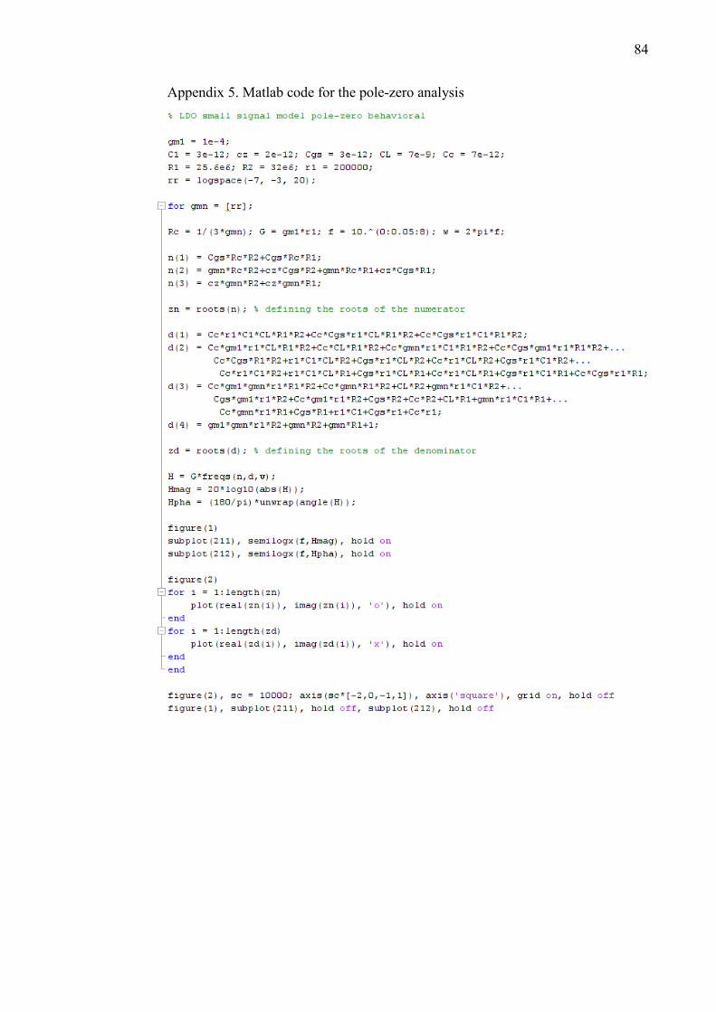
84
Appendix 5. Matlab code for the pole-zero analysis
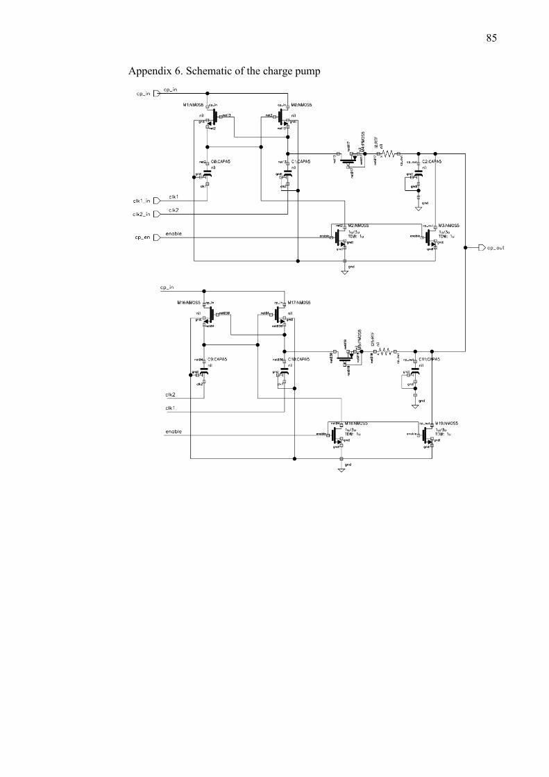
85
Appendix 6. Schematic of the charge pump

86
Appendix 7. Schematics of the designed LDO regulator