a fvf ldo regulator with dual-summed miller frequency
TRANSCRIPT
1304 IEEE TRANSACTIONS ON CIRCUITS AND SYSTEMS—I: REGULAR PAPERS, VOL. 61, NO. 5, MAY 2014
A FVF LDO Regulator With Dual-SummedMiller Frequency Compensation for WideLoad Capacitance Range ApplicationsXiao Liang Tan, Student Member, IEEE, Kuan Chuang Koay, Member, IEEE,Sau Siong Chong, Student Member, IEEE, and P. K. Chan, Senior Member, IEEE
Abstract—This paper presents a proposed Flipped Voltage Fol-lower (FVF) based output capacitorless low-dropout (OCL-LDO)regulator using Dual-Summed Miller Frequency Compensation(DSMFC) technique. Validated by UMC 65-nm CMOS process,the simulation results have shown that the proposed LDO regu-lator can be stabilized by a total compensation capacitanceof 8 pF for a load capacitance ranging from 10 pF to 10nF. It consumes 23.7 A quiescent current with a 1.2 V supplyvoltage. With a dropout voltage of 200 mV, the LDO regulator cansupport a maximum 50 mA load current. It can settle in less than1.7 s with a 1% accuracy for the whole range. The proposedLDO regulator is comparable to other reported works in terms offigure-of-merit (FOM). Most significantly, it can drive the widestrange of and achieve the highest ratio withrespect to the counterparts.
Index Terms—DSMFC, FVF, LDO regulator, Miller compensa-tion, wide load capacitance range.
I. INTRODUCTION
V OLTAGE regulators have been widely used to supplyvarious function blocks in battery powered devices.
A LDO regulator featuring a simple structure with fast re-sponse and low noise characteristics is very popular in powermanagement IC design [1]. However, the LDO regulatorsrelying on a F level off-chip capacitor to maintain stableoperation will limit their fully integration ability for modernSystem-on-Chips (SoC) [2]–[6]. As such, the output capacitor-less LDO (OCL-LDO) regulators have received much attentionfor fully on-chip applications.OCL-LDO regulators have been recently reported in
[7]–[17]. Among these designs, the Flipped Voltage Follower(FVF) based LDO regulators [8], [11]–[14] are attractive interms of simplicity, stability and fast transient responses. In[8], the FVF structure is implemented as drivers for the output.It gives a very fast response with a recovering time of 0.54ns. However, the quiescent current in this LDO regulator is 6mA. In addition, the LDO regulator is stabilized by a 600 pFon-chip decoupling capacitor. This results in large power andsilicon area consumptions. In [11], a Single-Transistor-ControlLDO regulator based on FVF structure is proposed. It has beenproven that the LDO regulator is stable without an off-chipcapacitor. In [12], a direct voltage spike detection scheme
Manuscript received August 23, 2013; revised December 03, 2013, January06, 2014; accepted January 12, 2014. Date of publication March 25, 2014; dateof current version April 24, 2014.The authors are with the School of Electrical and Electronic Engi-
neering, Nanyang Technological University, 639798 Singapore (e-mail:[email protected]; [email protected]; [email protected];[email protected]).Digital Object Identifier 10.1109/TCSI.2014.2309902
is adopted in the FVF structure to momentarily increase thequiescent current during load current switching. Hence, thetransient response of the regulator is improved. However,both topologies [11], [12] suffer from low loop gain due to itssimple folded structure [13]. As a result, an additional gainstage has been added in the feedback loop to boost the loopgain in [13] for improvement of both load and line regulations.Due to the additional gain stage, a Miller compensation capac-itor is required for circuit stability purpose at low quiescentpower.However, the conventional Miller compensation typically
supports small load capacitors. The LDO regulator in [13]is only able to drive a maximum 50 pF load capacitor witha minimum 3 mA load current at V. To furtherincrease the load capacitance driving capability, either thecompensation capacitor or the minimum load current mustbe increased to achieve a stable operation. This restricts itsapplication at the circuits with load capacitance starting fromfew ten pF to few hundred pF. However, for some digital circuitapplications [18] that require the LDO regulator to drive theon-chip capacitance of 3 nF or more. This creates a designchallenge on the FVF OCL-LDO regulators using standardMiller compensation technique in the context of low quiescentpower. In [14], based on a FVF output driving stage, an activecompensation scheme is implemented which can drive a loadcapacitance up to 1 nF. However, several poles and zerosare within the unity gain bandwidth frequency , thusleading to complicated pole-zero tracking. Furthermore, theLDO regulator may be susceptible to process and temperaturevariations since the stability is very much dependent on thepoles’ and zeros’ locations.In view of that, a Dual-Summed Miller Frequency Compen-
sation (DSMFC) technique is implemented in a FVF based LDOregulator topology [19]. The LDO regulator has been demon-strated in a very wide load capacitance range. Not only doesthe added Miller compensation stage form the dominant poletogether with the conventional Miller capacitor, it also shiftsthe non-dominant pole(s) to a higher frequency. In the reporteddual-summed Miller compensated LDO regulator [19], a lowoutput impedance power transistor driver [20] is realized asthe second non-inverting gain stage to improve the loop gain.Turning to the DSMFC network, the inverting driving transistorfor the second Miller amplifier is biased by a high impedancecurrent source with an open loop topology. To ensure a reliabledc operating region of the additional Miller stage, the powertransistor has to be sized larger at the expense of larger siliconarea so as to reduce the voltage swing at the Miller node.
1549-8328 © 2014 IEEE. Personal use is permitted, but republication/redistribution requires IEEE permission.See http://www.ieee.org/publications_standards/publications/rights/index.html for more information.

TAN et al.: FVF LDO REGULATOR 1305
Based on the scheme in [19], an improved FVF based LDOregulator using the DSMFC technique is proposed in this paper.In Section II, the frequency response of the proposed LDO reg-ulator is analyzed at different load capacitor and current
conditions. Besides, the detailed analysis for phase margin(PM), damping factor and gain margin (GM) is presented.Effect of PM and GM with respect to the load capacitors is alsoinvestigated. The simulated results and discussions of key pa-rameters are given in Section III. In Section IV, a comparisonwith other reported OCL-LDO regulators is given. Conclusionsare drawn in Section V.
II. PROPOSED FVF LDO REGULATOR WITH DSMFC
The schematic of the proposed LDO regulator is shown inFig. 1(a). The main loop contains a folded FVF gain stage,a non-inverting gain stage and a power MOS transistor. TheLDO regulator is compensated using a DSMFC block (dash en-closed area). It contains a standard Miller compensation capac-itor and an additional Miller compensation stage (
and ). Different from [19], the DSMFC in the proposedLDO regulator is biased using a passive resistor . This re-alization permits a reliable DC operating point to be achieved inabsence of high impedance node. As such, the power transistorcan be sized smaller with respect to that in [19].With the DSMFC technique, the dominant pole is formed
through the summing Miller effect which offers better stability.Besides, when comparing with Single Miller Compensation(SMC) counterpart, the DSMFC also shifts the non-dominantpole(s) to a higher frequency, especially under the followingthree conditions: (i) large with low , (ii) large withmoderate , and (iii) small with low . Since the DSMFCtechnique addresses the conservative stability issue for bothsmall and large , the proposed LDO regulator can achievedriving capability for a wide load capacitance range across thewhole load current range.The control voltage for is generated through a symmet-
rical OTA amplifier which is shown in Fig. 1(b). Since the max-imum load capacitor is in an nF range, to reduce the settlingtime from overshoot, an overshoot reduction branch (and ) is implemented to increase the sinking current momen-tarily.
A. Stability Analysis
To analyze the stability of the proposed LDO regulator, thesmall-signal model depicted in Fig. 1(c) is investigated. It is ob-tained by breaking the feedback loop at the output branch asshown in Fig. 1(a). It is noted that denotes the transcon-ductance whereas and are the equivalent output resis-tance and lumped output parasitic capacitance of the i-th gainstage, respectively. and are the 1st and 2nd Millercompensation capacitors. is the effective output resistancewhich includes the output resistance of power transistor and theloading resistance . is the load capacitance which has avalue ranging from 10 pF to 10 nF.
Fig. 1. (a) Schematic of the proposed FVF based LDO regulator with DSMFCindicate the loop breaking point). (b) Control voltage
generator. (c) Small-signal model of the proposed FVF LDO regulator.
(1)
The transfer function is derived with the following assump-tions: (i) and ; (ii)
and . It is obtained and expressed by (1), inwhich is the dc loop gain and are the three zeros.Based on the design parameters, locate at high frequencies,thus they can be ignored in the following analysis. In addition,
1306 IEEE TRANSACTIONS ON CIRCUITS AND SYSTEMS—I: REGULAR PAPERS, VOL. 61, NO. 5, MAY 2014
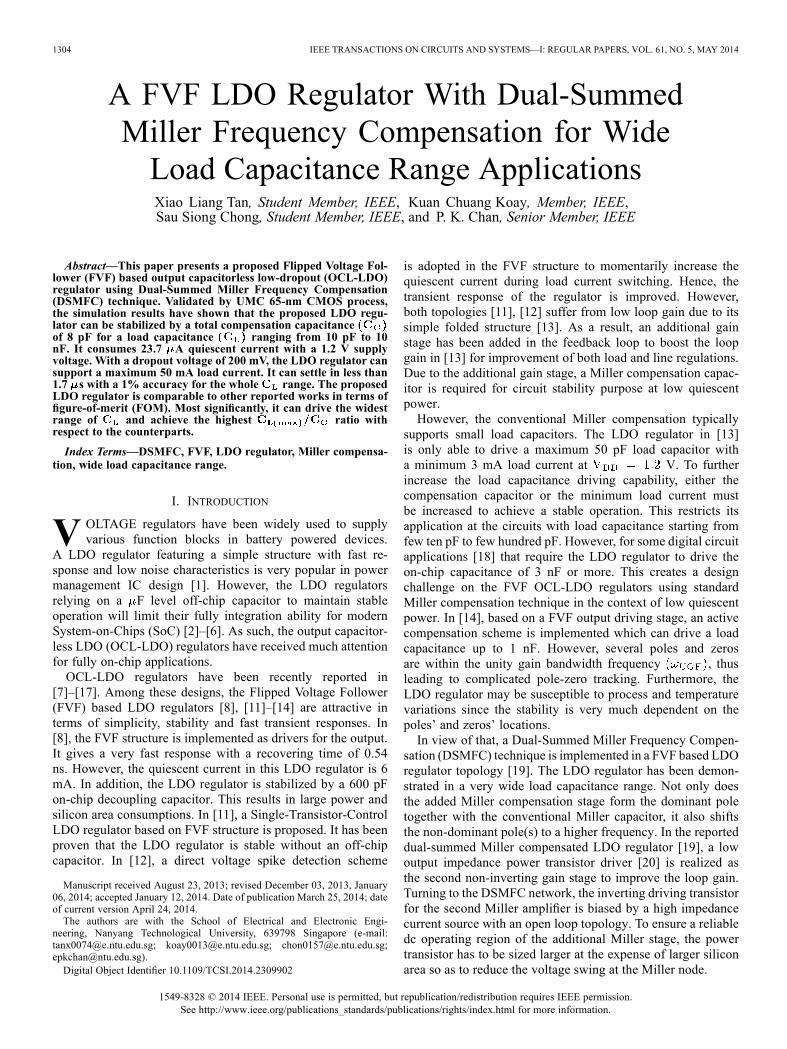
TABLE IPOLES AND ZERO LOCATIONS FOR SIX CASES
Fig. 2. Loop gain of the proposed FVF LDO regulator with poles and zerolocations for (a) large , (b) small .
the loop gain transfer function has two real poles - .Therefore, it can be simplified in the form as
-
(2)
Since the load capacitor varies from 10 pF to 10 nF with theload current switching between 0 and 50 mA, the stability of theOCL-LDO regulator is discussed at six different cases that dealwith the load capacitor corners at different load currents. Theyare given as follows:(1) Large with low , (2) Largewith moderate , (3) Large with high (4) Small withlow , (5) Small with moderate , (6) Small with high.The poles and zeros locations for six cases are summarized
in Table I and their relative locations are shown in Fig. 2(a) and
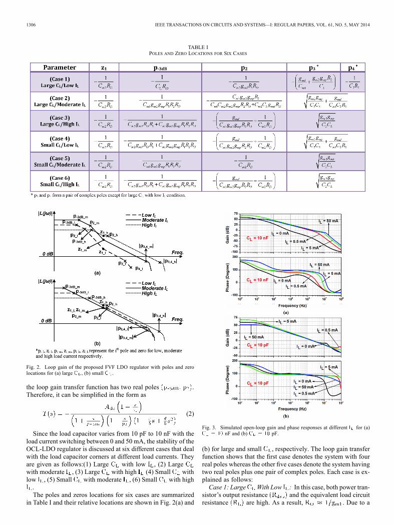
Fig. 3. Simulated open-loop gain and phase responses at different for (a)nF and (b) pF.
(b) for large and small , respectively. The loop gain transferfunction shows that the first case denotes the system with fourreal poles whereas the other five cases denote the system havingtwo real poles plus one pair of complex poles. Each case is ex-plained as follows:Case 1: Large With Low : In this case, both power tran-
sistor’s output resistance and the equivalent load circuitresistance are high. As a result, . Due to a
TAN et al.: FVF LDO REGULATOR 1307
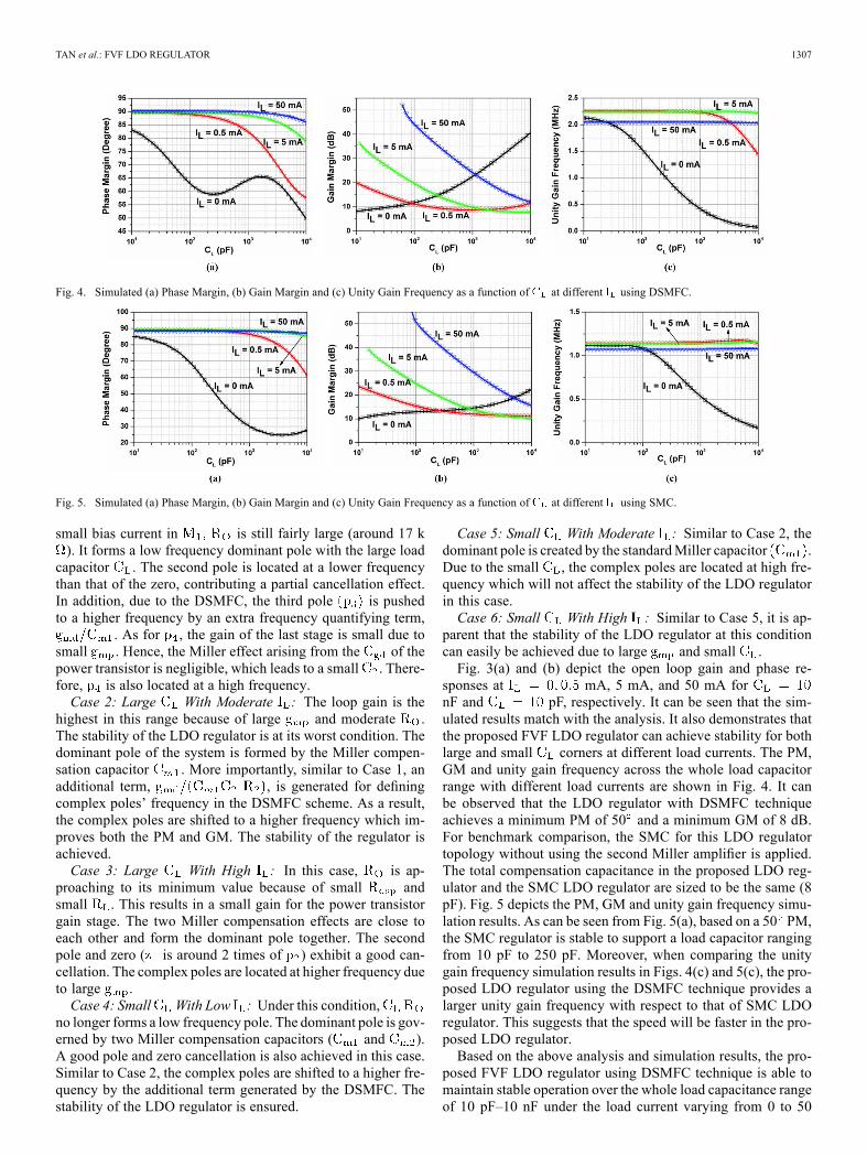
Fig. 4. Simulated (a) Phase Margin, (b) Gain Margin and (c) Unity Gain Frequency as a function of at different using DSMFC.
Fig. 5. Simulated (a) Phase Margin, (b) Gain Margin and (c) Unity Gain Frequency as a function of at different using SMC.
small bias current in is still fairly large (around 17 k). It forms a low frequency dominant pole with the large loadcapacitor . The second pole is located at a lower frequencythan that of the zero, contributing a partial cancellation effect.In addition, due to the DSMFC, the third pole is pushedto a higher frequency by an extra frequency quantifying term,
. As for , the gain of the last stage is small due tosmall . Hence, the Miller effect arising from the of thepower transistor is negligible, which leads to a small . There-fore, is also located at a high frequency.Case 2: Large With Moderate : The loop gain is the
highest in this range because of large and moderate .The stability of the LDO regulator is at its worst condition. Thedominant pole of the system is formed by the Miller compen-sation capacitor . More importantly, similar to Case 1, anadditional term, , is generated for definingcomplex poles’ frequency in the DSMFC scheme. As a result,the complex poles are shifted to a higher frequency which im-proves both the PM and GM. The stability of the regulator isachieved.Case 3: Large With High : In this case, is ap-
proaching to its minimum value because of small andsmall . This results in a small gain for the power transistorgain stage. The two Miller compensation effects are close toeach other and form the dominant pole together. The secondpole and zero ( is around 2 times of ) exhibit a good can-cellation. The complex poles are located at higher frequency dueto large .Case 4: Small With Low : Under this condition,
no longer forms a low frequency pole. The dominant pole is gov-erned by two Miller compensation capacitors ( and ).A good pole and zero cancellation is also achieved in this case.Similar to Case 2, the complex poles are shifted to a higher fre-quency by the additional term generated by the DSMFC. Thestability of the LDO regulator is ensured.
Case 5: Small With Moderate : Similar to Case 2, thedominant pole is created by the standardMiller capacitor .Due to the small , the complex poles are located at high fre-quency which will not affect the stability of the LDO regulatorin this case.Case 6: Small With High : Similar to Case 5, it is ap-
parent that the stability of the LDO regulator at this conditioncan easily be achieved due to large and small .Fig. 3(a) and (b) depict the open loop gain and phase re-
sponses at mA, 5 mA, and 50 mA fornF and pF, respectively. It can be seen that the sim-ulated results match with the analysis. It also demonstrates thatthe proposed FVF LDO regulator can achieve stability for bothlarge and small corners at different load currents. The PM,GM and unity gain frequency across the whole load capacitorrange with different load currents are shown in Fig. 4. It canbe observed that the LDO regulator with DSMFC techniqueachieves a minimum PM of 50 and a minimum GM of 8 dB.For benchmark comparison, the SMC for this LDO regulatortopology without using the second Miller amplifier is applied.The total compensation capacitance in the proposed LDO reg-ulator and the SMC LDO regulator are sized to be the same (8pF). Fig. 5 depicts the PM, GM and unity gain frequency simu-lation results. As can be seen from Fig. 5(a), based on a 50 PM,the SMC regulator is stable to support a load capacitor rangingfrom 10 pF to 250 pF. Moreover, when comparing the unitygain frequency simulation results in Figs. 4(c) and 5(c), the pro-posed LDO regulator using the DSMFC technique provides alarger unity gain frequency with respect to that of SMC LDOregulator. This suggests that the speed will be faster in the pro-posed LDO regulator.Based on the above analysis and simulation results, the pro-
posed FVF LDO regulator using DSMFC technique is able tomaintain stable operation over the whole load capacitance rangeof 10 pF–10 nF under the load current varying from 0 to 50
1308 IEEE TRANSACTIONS ON CIRCUITS AND SYSTEMS—I: REGULAR PAPERS, VOL. 61, NO. 5, MAY 2014
mA. Particularly, the DSMFC shows a significant improvementunder three conditions: (i) large with low , (ii) largewith moderate , and (iii) small with low . This extendsthe load capacitance range because it addresses the conservativestability issue for both small and large .
B. Phase Margin Under Variations
As can be seen in Fig. 4(a), at small condition, the PMplot shows a “quadratic” behavior. When increases, the PMdrops from 83 to around 60 and then increases again. Ifcontinues to increase, the PM will drop again. The phenomenonis due to shifting of the pole when varies from small to largevalues. The analysis can be divided into two parts: (i) complexpole region for small and (ii) real pole region for large .Region i: In this region, owing to small , the dominant
pole is formed by the two Miller compensation capacitors (and ). It is independent of and gives a constant unitygain frequency as follows:
(3)
In addition, the loop system gives a pair of complex poleswhich are given by
(4)
It can be seen that the location of the complex poles is in-versely proportional to . As increases, the complex poles’frequency decreases and appears to be closer to the unit gain fre-quency. As a consequence, the PM is reduced and the stabilityof the LDO regulator becomes worse. This explains why the PMplot in Fig. 4(a) shows a continuous drop first when is lessthan 250 pF.Region ii: For large , the output capacitor also plays a role
in the dominant pole formation. The dominant pole is given as
-
(5)
which leads to a dependent unity gain frequency as follows:
(6)
Since the zero generated from the DSMFC is fixed at(1) and the second pole locates at a lower
times) frequency, the loop phase response gives asmall peak around the zero location. Based on the reason, whenunity gain frequency continues to reduce as increases, thePM will increase and then drop again, depending on the relativelocation of the unity gain bandwidth and the fixed zero .
TABLE IIDAMPING FACTOR AND GM FOR CASES EXHIBITING COMPLEX POLE PAIR
C. Damping Factor and Gain Margin Under Variations
Damping factor is critical for the LDO regulator stabilitywhen a pair of complex poles exist in the loop gain transferfunction (case 2 to case 6 in Table I). Consider the second-orderterms in (2) with a standard form as
(7)
where is the damping factor and is the frequency of thecomplex poles.Although the DSMFC increases the frequency of the com-
plex poles which in turn improves the PM and GM, the of thecomplex poles should be designed properly to avoid large fre-quency peaking and maintain a good GM. If it is assumed thatthe second pole and the zero generated by the DSMFC canceleach other, based on [21], the relationship between and PM aswell as and GM in a second-order system is approximately asfollows:
(8)
(9)
From (8) and (9), a large increases the GM but it gives alarge negative phase shift which reduces the PM. On the otherhand, a small reduces the GM and makes a sharp phase dropwhich can lead to a 0 PM.Based on transfer function in (1), the general expression for
the in the second-order system defined in (7) is obtained as(10), shown at the bottom of the page.
(10)
TAN et al.: FVF LDO REGULATOR 1309
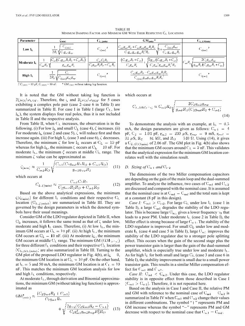
TABLE IIIMINIMUM DAMPING FACTOR AND MINIMUM GM WITH THEIR RESPECTIVE LOCATIONS
It is noted that the GM without taking log function is. Therefore, the and for 5 cases
exhibiting a complex pole pair (case 2–case 6 in Table I) aresummarized in Table II. For case I in Table I (large , low), the system displays four real poles, thus it is not included
in Table II and the respective analysis.From Table II, when increases, the observation is in the
following. (i) For low and small (case 4), increases. (ii)For moderate (case 2 and case 5), will reduce first and thenincrease again. (iii) For high (case 3 and case 6), decreases.Therefore, the minimum for low occurs at pFwhereas for high , the minimum occurs at nF. Formoderate , the minimum occurs at middle range. Theminimum value can be approximated as
(11)
which occurs at
(12)
Based on the above analytical expressions, the minimumfor different conditions and their respective
location are summarized in Table III. They aregoverned by the design parameters in which the denoted sym-bols have their usual meanings.Consider GM of the LDO regulator depicted in Table II, whenincreases, it follows the same trend as that of under low,
moderate and high cases. Therefore, (i) At low , the min-imum GM occurs at pF. (ii) At high , the minimumGM occurs at nF. (iii) At moderate , the minimumGM occurs at middle range. The minimum GMfor three different conditions and their respective location
are also summarized in Table III. Turning to theGM plot of the proposed LDO regulator in Fig. 4(b), at ,the minimum GM location is at pF. On the other hand,at and 50 mA, the minimum GM location is atnF. This matches the minimum GM location analysis for lowand high conditions, respectively.At moderate , through derivation and Binomial approxima-
tions, the minimumGM (without taking log function) is approx-imated as
(13)
which occurs at
(14)
To demonstrate the analysis with an example, atmA, the design parameters are given as follows:pF, pF, S, mS,
S, k , and . Using (14), it givesa of 2.06 nF. The GM plot in Fig. 4(b) also showsthat the minimum GM occurs around nF. This validatesthat the analytical expression for the minimumGM location cor-relates well with the simulation result.
D. Sizing of and
The dimensions of the two Miller compensation capacitorsare depending on the gain of themain loop and the dual-summedamplifier. To analyze the influence, two cases of andare discussed and compared with the nominal case. It is assumedthat the nominal case is at and the total sum is keptat a constant (8 pF in this design).Case I: . For large under low (case 1 in
Table I), a large degrades the stability of the LDO regu-lator. This is because large gives a lower frequency thatleads to a poor PM. Under moderate (case 2 in Table I), theMiller effect is strong because of large . The stability of theLDO regulator is improved. For small under low and mod-erate (case 4 and case 5 in Table I), large improves thestability of the LDO regulator due to a stronger pole splittingeffect. This occurs when the gain of the second stage plus thepower transistor gain is larger than the gain of the dual-summedamplifier, which is especially true under low and moderate .As for high for both small and large (case 3 and case 6 inTable I), the stability improvement is small due to a small powertransistor gain. This results in a similar Miller compensation ef-fect for and .Case II: . Under this case, the LDO regulator
stability is in opposite effect from those described in Case I. Therefore, it is not repeated here.
Based on the analysis in Case I and Case II, the relative PMand GM with reference to the nominal case of issummarized in Table IVwhen and change their valuesin different combinations. The symbol “ ” represents PM andGM increase whereas the symbol “ ” represents PM and GMdecrease with respect to the nominal case that .
1310 IEEE TRANSACTIONS ON CIRCUITS AND SYSTEMS—I: REGULAR PAPERS, VOL. 61, NO. 5, MAY 2014
TABLE IVRELATIVE PM AND GM FOR DIFFERENT COMBINATIONS WITH
REFERENCE TO NOMINAL CASE
TABLE VPM AND GM FOR DIFFERENT COMBINATIONS
Table V gives the simulated PM andGM for the capacitor pair( ) which corresponds to the design values of (5 pF, 3pF), (4 pF, 4 pF) and (3 pF, 5 pF). For example one, atmA (low ) and pF (small ), when pF,
pF, both PM and GM are larger than that of nominalcase ( pF, pF). For example two, atmA (low ) and nF (large ), when pF,
pF, both PM and GM are smaller than the nominalcase. This confirms that the simulation results on the size ofand correlate well with the expected behavior as indicatedin Table IV.
III. SIMULATION RESULTS AND DISCUSSIONS
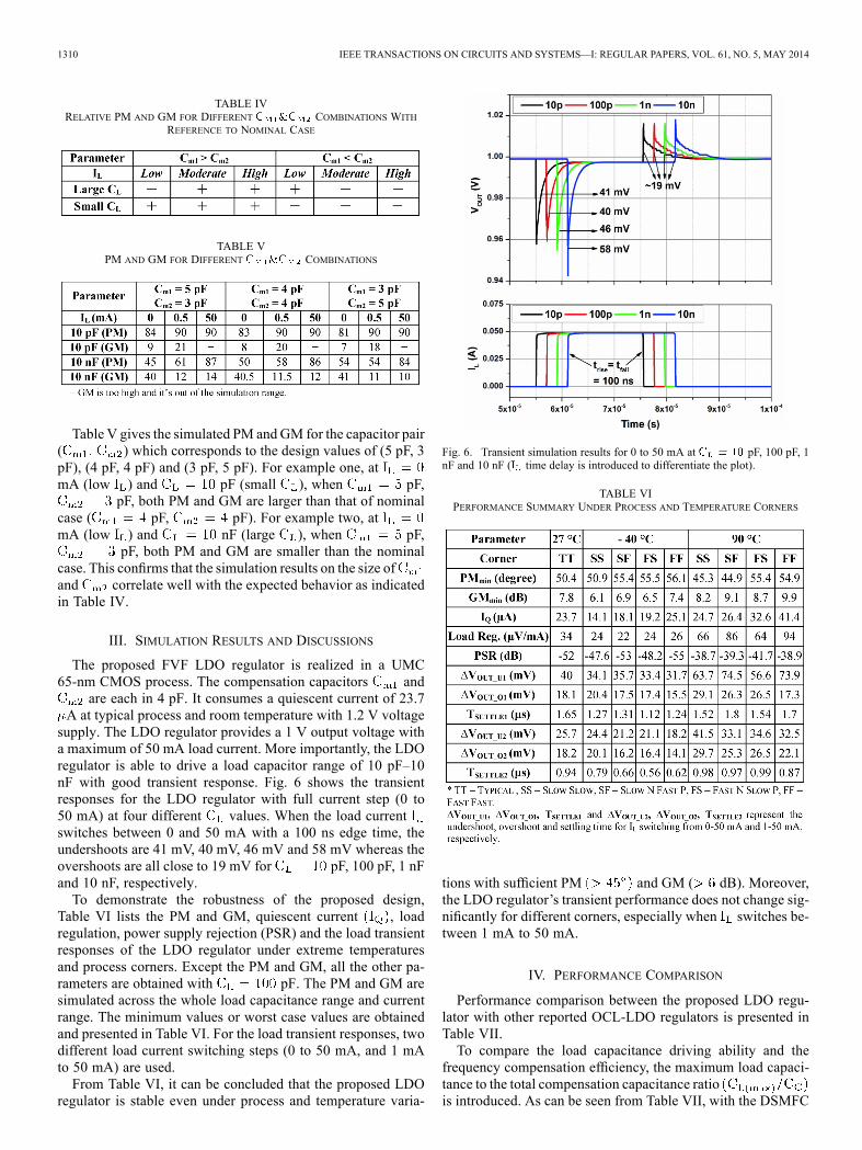
The proposed FVF LDO regulator is realized in a UMC65-nm CMOS process. The compensation capacitors and
are each in 4 pF. It consumes a quiescent current of 23.7A at typical process and room temperature with 1.2 V voltagesupply. The LDO regulator provides a 1 V output voltage witha maximum of 50 mA load current. More importantly, the LDOregulator is able to drive a load capacitor range of 10 pF–10nF with good transient response. Fig. 6 shows the transientresponses for the LDO regulator with full current step (0 to50 mA) at four different values. When the load currentswitches between 0 and 50 mA with a 100 ns edge time, theundershoots are 41 mV, 40 mV, 46 mV and 58 mV whereas theovershoots are all close to 19 mV for pF, 100 pF, 1 nFand 10 nF, respectively.To demonstrate the robustness of the proposed design,
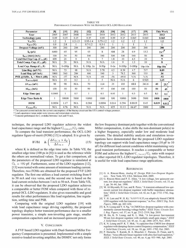
Table VI lists the PM and GM, quiescent current , loadregulation, power supply rejection (PSR) and the load transientresponses of the LDO regulator under extreme temperaturesand process corners. Except the PM and GM, all the other pa-rameters are obtained with pF. The PM and GM aresimulated across the whole load capacitance range and currentrange. The minimum values or worst case values are obtainedand presented in Table VI. For the load transient responses, twodifferent load current switching steps (0 to 50 mA, and 1 mAto 50 mA) are used.From Table VI, it can be concluded that the proposed LDO
regulator is stable even under process and temperature varia-
Fig. 6. Transient simulation results for 0 to 50 mA at pF, 100 pF, 1nF and 10 nF ( time delay is introduced to differentiate the plot).
TABLE VIPERFORMANCE SUMMARY UNDER PROCESS AND TEMPERATURE CORNERS
tions with sufficient PM and GM ( dB). Moreover,the LDO regulator’s transient performance does not change sig-nificantly for different corners, especially when switches be-tween 1 mA to 50 mA.
IV. PERFORMANCE COMPARISON
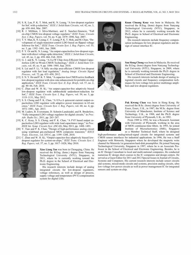
Performance comparison between the proposed LDO regu-lator with other reported OCL-LDO regulators is presented inTable VII.To compare the load capacitance driving ability and the
frequency compensation efficiency, the maximum load capaci-tance to the total compensation capacitance ratiois introduced. As can be seen from Table VII, with the DSMFC
TAN et al.: FVF LDO REGULATOR 1311
TABLE VIIPERFORMANCE COMPARISON WITH THE REPORTED OCL-LDO REGULATORS
technique, the proposed LDO regulator achieves the widestload capacitance range and the highest ratio.To compare the load transient performance, the OCL-LDO
regulator figure-of-merit (FOM) [13] is adopted. It is given by
(15)
where K is defined as the edge time ratio. In Table VII, thesmallest edge time (100 ps in [8]) is used as the reference whilethe others are normalized values. To get a fair comparison, allthe parameters of the proposed LDO regulator is simulated at
pF. Furthermore, some of the LDO regulators [12],[13] were tested with some amount of minimum loading current.Therefore, two FOMs are obtained for the proposed FVF LDOregulator. The first one utilizes a load current switching from 0to 50 mA and vice versa, and the second one is based on theload current switches between 1 mA to 50 mA. From Table VII,it can be observed that the proposed LDO regulator achievesa comparable or better FOM when compared with those of re-ported OCL-LDO regulators. It also gives reasonable and goodresults for other performances like load regulation, line regula-tion, settling time and PSR.Comparing with the original LDO regulator [19] with
wide load capacitance range driving capability, the proposedtopology displays better transient performance due to a smallerpower transistor, a simple non-inverting gain stage, smallercompensation capacitors and an increased quiescent power.
V. CONCLUSION
A FVF based LDO regulator with Dual-Summed Miller Fre-quency Compensation is presented. Implemented with a simpleresistive-loaded inverting amplifier, the DSMFC not only forms
the low frequency dominant pole together with the conventionalMiller compensation, it also shifts the non-dominant pole(s) toa higher frequency, especially under low and moderate loadcurrents. The detailed stability analysis and simulation inves-tigations have demonstrated that the proposed LDO regulatortopology can support wide load capacitance range (10 pF to 10nF) for different load current conditions whilst maintaining verygood transient performance. It reaches a comparable or betterFOM and achieves the highest ratio with respectto other reported OCL-LDO regulator topologies. Therefore, itis useful for wide load capacitance range applications.
REFERENCES[1] G. A. Rincon-Mora, Analog IC Design With Low-Dropout Regula-
tors. New York, NY, USA: McGraw-Hill, 2009.[2] G. Rincon-Mora and P. E. Allen, “A low-voltage, low quiescent cur-
rent, low drop-out regulator,” IEEE J. Solid-State Circuits, vol. 33, no.1, pp. 36–44, Jan. 1998.
[3] M. Al-Shyoukh, H. Lee, and R. Perez, “A transient-enhanced low-qui-escent current low-dropout regulator with buffer impedance attenua-tion,” IEEE J. Solid-State Circuits, vol. 42, no. 8, pp. 1732–1742, Aug.2007.
[4] Y. H. Lam and W. H. Ki, “A 0.9 V 0.35 m adaptively biased CMOSLDO regulator with fast transient response,” in Proc. ISSCC Dig. Tech.Papers, 2008, pp. 442–626.
[5] K. N. Leung and Y. S. Ng, “A CMOS low-dropout regulator with a mo-mentarily current-boosting voltage buffer,” IEEE Trans. Circuits Syst.I, Reg. Papers, vol. 57, no. 9, pp. 2312–2319, Sep. 2010.
[6] M. Ho, K. N. Leung, and K. L. Mak, “A low-power fast-transient90-nm low-dropout regulator with multiple small-gain stages,” IEEEJ. Solid-State Circuits, vol. 45, no. 11, pp. 2466–2475, Nov. 2010.
[7] K. N. Leung and P. K. T. Mok, “A capacitor-free CMOS low-dropoutregulator with damping-factor-control frequency compensation,” IEEEJ. Solid-State Circuits, vol. 38, no. 10, pp. 1691–1702, Oct. 2003.
[8] P. Hazucha, T. Karnik, B. A. Bloechel, C. Parsons, D. Finan, and S.Borkar, “Area-efficient linear regulator with ultra-fast load regulation,”IEEE J. Solid-State Circuits, vol. 40, no. 4, pp. 933–940, Apr. 2005.
1312 IEEE TRANSACTIONS ON CIRCUITS AND SYSTEMS—I: REGULAR PAPERS, VOL. 61, NO. 5, MAY 2014
[9] S. K. Lau, P. K. T. Mok, and K. N. Leung, “A low-dropout regulatorfor SoC with q-reduction,” IEEE J. Solid-State Circuits, vol. 42, no. 3,pp. 658–664, Mar. 2007.
[10] R. J. Milliken, J. Silva-Martinez, and E. Sanchez-Sinencio, “Fullon-chip CMOS low-dropout voltage regulator,” IEEE Trans. CircuitsSyst. I, Reg. Papers, vol. 54, no. 9, pp. 1879–1890, Sep. 2007.
[11] T. Y.Man, K. N. Leung, C. Y. Leung, P. K. T.Mok, andM. Chan, “De-velopment of single-transistor-control LDO based on flipped voltagefollower for SoC,” IEEE Trans. Circuits Syst. I, Reg. Papers, vol. 55,no. 5, pp. 1392–1401, Jun. 2008.
[12] P. Y. Or and K. N. Leung, “An output-capacitorless low-dropout regu-lator with direct voltage-spike detection,” IEEE J. Solid-State Circuits,vol. 45, no. 2, pp. 458–466, Feb. 2010.
[13] G. J. and K. N. Leung, “A 6- W Chip-Area-Efficient Output-Capac-itorless LDO in 90-nm CMOS Technology,” IEEE J. Solid-State Cir-cuits, vol. 45, no. 9, pp. 1896–1905, Sep. 2010.
[14] S. Lai and P. Li, “A fully on-chip area-efficient CMOS low-dropoutregulator with fast load regulation,” Analog Integr. Circuits SignalProcess., vol. 72, pp. 433–450, 2012.
[15] E. N. Y. Ho and P. K. T.Mok, “A capacitor-less CMOS active feedbacklow-dropout regulator with slew-rate enhancement for portable on-chipapplication,” IEEE Trans. Circuits Syst. II, Exp. Briefs, vol. 57, no. 2,pp. 80–84, Feb. 2010.
[16] C. Zhan and W. H. Ki, “An output-capacitor-free adaptively biasedlow-dropout regulator with subthreshold undershoot-reduction forSoC,” IEEE Trans. Circuits Syst. I, Reg. Papers, vol. 59, no. 5, pp.1119–1131, May 2012.
[17] S. S. Chong and P. K. Chan, “A 0.9- A quiescent current output-ca-pacitorless LDO regulator with adaptive power transistors in 65-nmcmos,” IEEE Trans. Circuits Syst. I, Reg. Papers, vol. 60, no. 4, pp.1072–1081, Apr. 2013.
[18] M. Luders, B. Eversmann, D. Schmitt-Landsiedel, and R. Brederlow,“Fully-integrated LDO voltage regulator for digital circuits,” in Proc.Adv. Radio Sci., 2011, pp. 263–267.
[19] K. C. Koay, S. S. Chong, and P. K. Chan, “A FVF based output ca-pacitorless LDO regulator with wide load capacitance range,” in Proc.IEEE Int. Symp. Circuits Syst. (ISCAS), May 2013, pp. 1488–1491.
[20] Y. Tian and P. K. Chan, “Design of high-performance analog circuitusing wideband gm-enchanced MOS composite transistor,” IEICETrans. Electron., vol. E93-C, pp. 1199–1208, 2010.
[21] C. Zhan and W. H. Ki, “Output-capacitor-free adaptively biased low-dropout regulator for system-on-chips,” IEEE Trans. Circuits Syst. I,Reg. Papers, vol. 57, no. 5, pp. 1017–1028, May 2010.
Xiao Liang Tan was born in Chongqing, China. Hereceived the B.Eng. (hons.) degree from NanyangTechnological University (NTU), Singapore, in2011, where he is currently working toward thePh.D. degree in the School of Electrical and Elec-tronic Engineering.His research interests include design of analog
integrated circuits for low-dropout regulators,voltage references, as well as design of process,supply voltage and temperature (PVT) compensationsystem for digital LSIs.
Kuan Chuang Koay was born in Malaysia. Hereceived the B.Eng. (hons) degree from NanyangTechnological University (NTU), Singapore, in2012, where he is currently working towards thePh.D. degree in School of Electrical and ElectronicEngineering.His research interests include frequency compen-
sation techniques for low-dropout regulators and de-sign of sensor interface IC.
Sau Siong Chongwas born inMalaysia. He receivedthe B.Eng. (hons) degree from Nanyang Technolog-ical University (NTU), Singapore, in 2009, wherehe is currently working towards the Ph.D. degree inSchool of Electrical and Electronic Engineering.His research interests include design of analog in-
tegrated circuits and frequency compensation tech-niques for low-voltage low-power multistage ampli-fiers and low-dropout regulators.
Pak Kwong Chan was born in Hong Kong. Hereceived the B.Sc. (hons) degree from University ofEssex, Essex, U.K., in 1987, the M.Sc. degree fromUniversity of Manchester, Institute of Science andTechnology, U.K., in 1988, and the Ph.D. degreefrom University of Plymouth, U.K., in 1992.From 1989 to 1992, he was a Research Assistant
with University of Plymouth, working in the areaof MOS continuous-time filters. In 1993, he joinedInstitute of Microelectronics (IME), Singaporeas a Member Technical Staff, where he designed
high-performance analog/mixed-signal circuits for integrated systems andCMOS sensor interfaces for industrial applications. In 1996, He was a StaffEngineer with Motorola, Singapore where he developed the magnetic writechannel for Motorola 1st generation hard-disk preamplifier. He joined NanyangTechnological University, Singapore in 1997, where he is an Associate Pro-fessor in the School of Electrical and Electronic Engineering. Besides, he isan IC Design Consultant to local and multi-national companies. He conductednumerous IC design short courses to the IC companies and design centers. Heserved as a Guest Editor for 2011 and 2012 Special Issues in Journal of Circuits,Systems and Computers. His current research interests include sensor circuitsand systems, mixed-mode circuits and systems, precision analog circuits, ultralow-voltage low-power circuits as well as power management IC for integratedsensors and system-on-chip.
本文献由“学霸图书馆-文献云下载”收集自网络,仅供学习交流使用。
学霸图书馆(www.xuebalib.com)是一个“整合众多图书馆数据库资源,
提供一站式文献检索和下载服务”的24 小时在线不限IP
图书馆。
图书馆致力于便利、促进学习与科研,提供最强文献下载服务。
图书馆导航:
图书馆首页 文献云下载 图书馆入口 外文数据库大全 疑难文献辅助工具