single-output ldo regulator variable output ldo … · single-output ldo regulator 1a variable...
TRANSCRIPT
Product structure : Silicon monolithic integrated circuit This product is not designed for protection against radioactive rays
1/18 TSZ02201-0T2T0AZ00060-1-2© 2013 ROHM Co., Ltd. All rights reserved. TSZ22111・14・001 08.Feb.2013 Rev.001
Datasheet
www.rohm.com
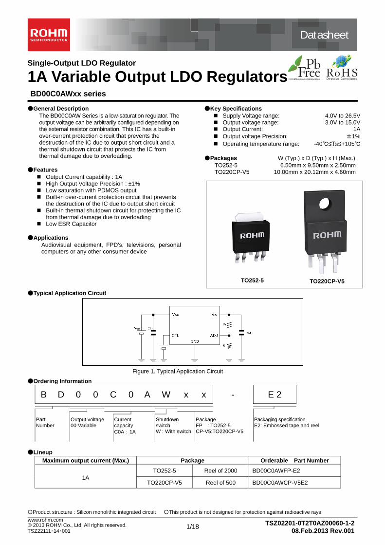
Single-Output LDO Regulator 1A Variable Output LDO Regulators BD00C0AWxx series
General Description
The BD00C0AW Series is a low-saturation regulator. The output voltage can be arbitrarily configured depending on the external resistor combination. This IC has a built-in over-current protection circuit that prevents the destruction of the IC due to output short circuit and a thermal shutdown circuit that protects the IC from thermal damage due to overloading.
Features
Output Current capability : 1A High Output Voltage Precision : ±1% Low saturation with PDMOS output Built-in over-current protection circuit that prevents
the destruction of the IC due to output short circuit Built-in thermal shutdown circuit for protecting the IC
from thermal damage due to overloading Low ESR Capacitor
Applications
Audiovisual equipment, FPD’s, televisions, personal computers or any other consumer device
Key Specifications
Supply Voltage range: 4.0V to 26.5V Output voltage range: 3.0V to 15.0V Output Current: 1A Output voltage Precision: ±1% Operating temperature range: -40≤Ta≤+105
Packages W (Typ.) x D (Typ.) x H (Max.)
TO252-5 6.50mm x 9.50mm x 2.50mm TO220CP-V5 10.00mm x 20.12mm x 4.60mm
Typical Application Circuit Ordering Information
B D 0 0 C 0 A W x x - E 2
Part Number
Output voltage 00:Variable
Current capacity C0A:1A
Shutdown switch W : With switch
Package FP : TO252-5 CP-V5:TO220CP-V5
Packaging specification E2: Embossed tape and reel
Lineup
Maximum output current (Max.) Package Orderable Part Number
1A TO252-5 Reel of 2000 BD00C0AWFP-E2
TO220CP-V5 Reel of 500 BD00C0AWCP-V5E2
TO252-5 TO220CP-V5
Figure 1. Typical Application Circuit
DatasheetDatasheet
2/18 TSZ02201-0T2T0AZ00060-1-2© 2013 ROHM Co., Ltd. All rights reserved. TSZ22111・15・001 08.Feb.2013 Rev.001
BD00C0AWxx series
www.rohm.com
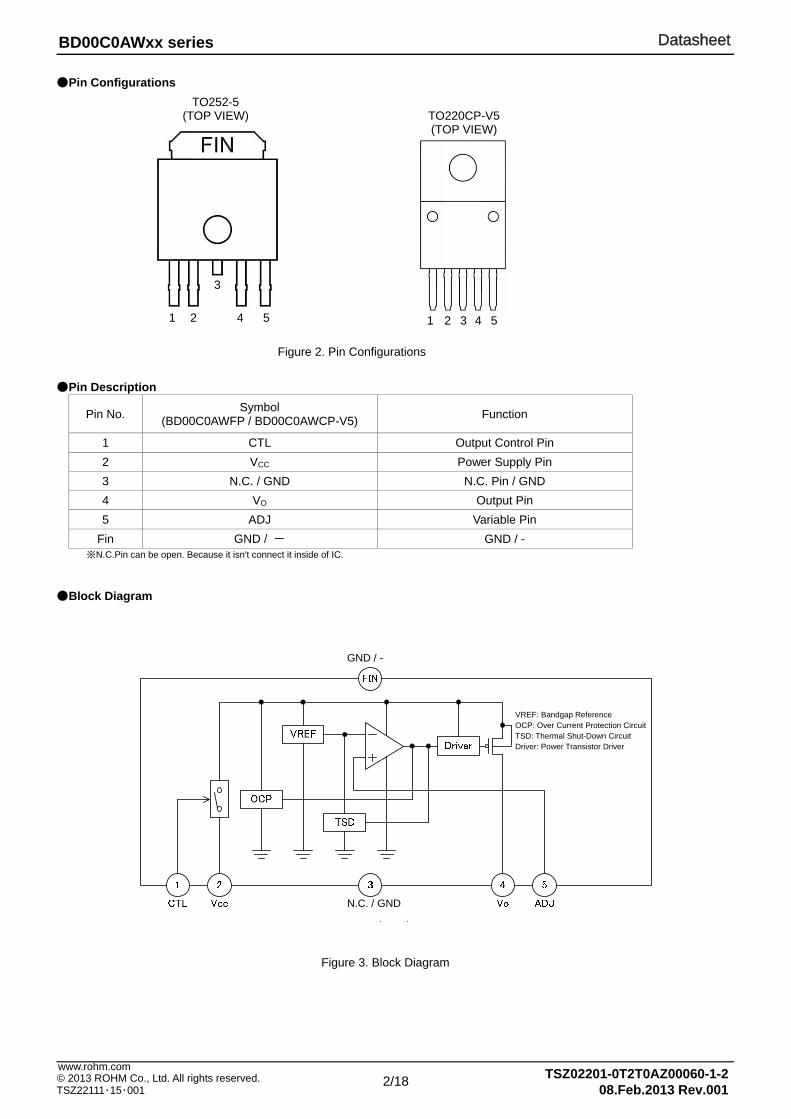
Pin Configurations Pin Description
Pin No. Symbol (BD00C0AWFP / BD00C0AWCP-V5) Function
1 CTL Output Control Pin 2 VCC Power Supply Pin 3 N.C. / GND N.C. Pin / GND 4 VO Output Pin 5 ADJ Variable Pin
Fin GND / - GND / - ※N.C.Pin can be open. Because it isn't connect it inside of IC. Block Diagram
TO252-5 (TOP VIEW)
1 2
3
4 5
TO220CP-V5(TOP VIEW)
1 2 3 4 5
Figure 3. Block Diagram
Figure 2. Pin Configurations
GND / -
N.C. / GND
VREF: Bandgap Reference OCP: Over Current Protection Circuit TSD: Thermal Shut-Down Circuit Driver: Power Transistor Driver
DatasheetDatasheet
3/18 TSZ02201-0T2T0AZ00060-1-2© 2013 ROHM Co., Ltd. All rights reserved. TSZ22111・15・001 08.Feb.2013 Rev.001
BD00C0AWxx series
www.rohm.com
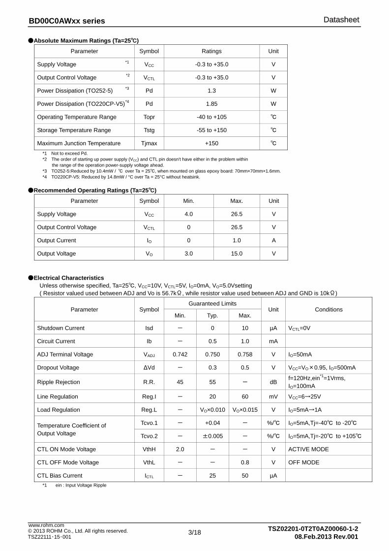
Absolute Maximum Ratings (Ta=25)
Parameter Symbol Ratings Unit
Supply Voltage *1 VCC -0.3 to +35.0 V
Output Control Voltage *2 VCTL -0.3 to +35.0 V
Power Dissipation (TO252-5) *3 Pd 1.3 W
Power Dissipation (TO220CP-V5) *4 Pd 1.85 W
Operating Temperature Range Topr -40 to +105
Storage Temperature Range Tstg -55 to +150
Maximum Junction Temperature Tjmax +150 *1 Not to exceed Pd. *2 The order of starting up power supply (VCC) and CTL pin doesn't have either in the problem within
the range of the operation power-supply voltage ahead. *3 TO252-5:Reduced by 10.4mW / over Ta = 25, when mounted on glass epoxy board: 70mm×70mm×1.6mm. *4 TO220CP-V5: Reduced by 14.8mW / °C over Ta = 25°C without heatsink.
Recommended Operating Ratings (Ta=25)
Parameter Symbol Min. Max. Unit
Supply Voltage VCC 4.0 26.5 V
Output Control Voltage VCTL 0 26.5 V
Output Current IO 0 1.0 A
Output Voltage VO 3.0 15.0 V
Electrical Characteristics
Unless otherwise specified, Ta=25, VCC=10V, VCTL=5V, IO=0mA, VO=5.0Vsetting ( Resistor valued used between ADJ and Vo is 56.7kΩ, while resistor value used between ADJ and GND is 10kΩ)
Parameter Symbol Guaranteed Limits
Unit Conditions Min. Typ. Max.
Shutdown Current Isd - 0 10 µA VCTL=0V
Circuit Current Ib - 0.5 1.0 mA
ADJ Terminal Voltage VADJ 0.742 0.750 0.758 V IO=50mA
Dropout Voltage ΔVd - 0.3 0.5 V VCC=VO×0.95, IO=500mA
Ripple Rejection R.R. 45 55 - dB f=120Hz,ein*1=1Vrms, IO=100mA
Line Regulation Reg.I - 20 60 mV VCC=6→25V
Load Regulation Reg.L - VO×0.010 VO×0.015 V IO=5mA→1A
Temperature Coefficient of Output Voltage
Tcvo.1 - +0.04 - %/ IO=5mA,Tj=-40 to -20
Tcvo.2 - ±0.005 - %/ IO=5mA,Tj=-20 to +105
CTL ON Mode Voltage VthH 2.0 - - V ACTIVE MODE
CTL OFF Mode Voltage VthL - - 0.8 V OFF MODE
CTL Bias Current ICTL - 25 50 µA *1 ein : Input Voltage Ripple
DatasheetDatasheet
4/18 TSZ02201-0T2T0AZ00060-1-2© 2013 ROHM Co., Ltd. All rights reserved. TSZ22111・15・001 08.Feb.2013 Rev.001
BD00C0AWxx series
www.rohm.com
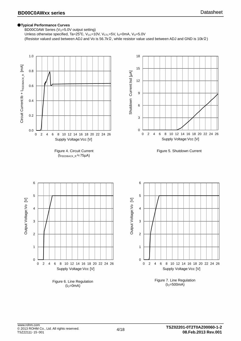
Typical Performance Curves BD00C0AW Series (VO=5.0V output setting) Unless otherwise specified, Ta=25, VCC=10V, VCTL=5V, IO=0mA, VO=5.0V (Resistor valued used between ADJ and Vo is 56.7kΩ, while resistor value used between ADJ and GND is 10kΩ)
Figure 4. Circuit Current (IFEEDBACK_R≒75µA)
Figure 5. Shutdown Current
Figure 6. Line Regulation (IO=0mA)
Figure 7. Line Regulation (IO=500mA)
0.0
0.2
0.4
0.6
0.8
1.0
0 2 4 6 8 10 12 14 16 18 20 22 24 26
Circ
uit C
urre
nt:Ib
+ I F
EED
BAC
K_R
[mA]
Supply Voltage:Vcc [V]
0
3
6
9
12
15
18
0 2 4 6 8 10 12 14 16 18 20 22 24 26Sh
utdo
wn
Cur
rent
:Isd
[μA]
Supply Voltage:Vcc [V]
0
1
2
3
4
5
6
0 2 4 6 8 10 12 14 16 18 20 22 24 26
Out
put V
olta
ge:V
o [V
]
Supply Voltage:Vcc [V]
0
1
2
3
4
5
6
0 2 4 6 8 10 12 14 16 18 20 22 24 26
Out
put V
olta
ge:V
o [V
]
Supply Voltage:Vcc [V]
DatasheetDatasheet
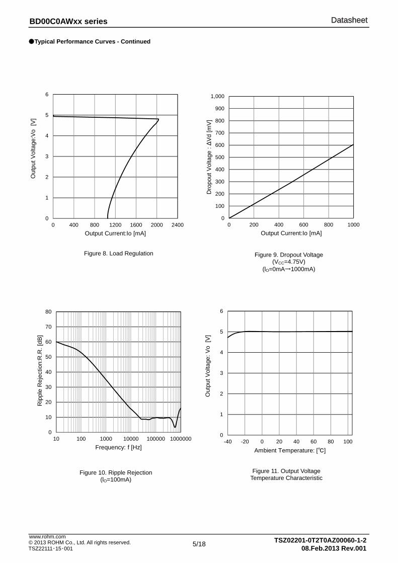
5/18 TSZ02201-0T2T0AZ00060-1-2© 2013 ROHM Co., Ltd. All rights reserved. TSZ22111・15・001 08.Feb.2013 Rev.001
BD00C0AWxx series
www.rohm.com
Figure 8. Load Regulation
Typical Performance Curves - Continued
Figure 9. Dropout Voltage (VCC=4.75V)
(lO=0mA→1000mA)
Figure 10. Ripple Rejection (lO=100mA)
Figure 11. Output Voltage Temperature Characteristic
0
1
2
3
4
5
6
0 400 800 1200 1600 2000 2400
Out
put V
olta
ge:V
o [V
]
Output Current:Io [mA]
0
100
200
300
400
500
600
700
800
900
1,000
0 200 400 600 800 1000
Dro
pout
Vol
tage
:Δ
Vd [m
V]
Output Current:Io [mA]
0
10
20
30
40
50
60
70
80
10 100 1000 10000 100000 1000000
Rip
ple
Rej
ectio
n:R
.R. [
dB]
Frequency: f [Hz]
0
1
2
3
4
5
6
-40 -20 0 20 40 60 80 100
Out
put V
olta
ge: V
o [V
]
Ambient Temperature: []
DatasheetDatasheet
6/18 TSZ02201-0T2T0AZ00060-1-2© 2013 ROHM Co., Ltd. All rights reserved. TSZ22111・15・001 08.Feb.2013 Rev.001
BD00C0AWxx series
www.rohm.com
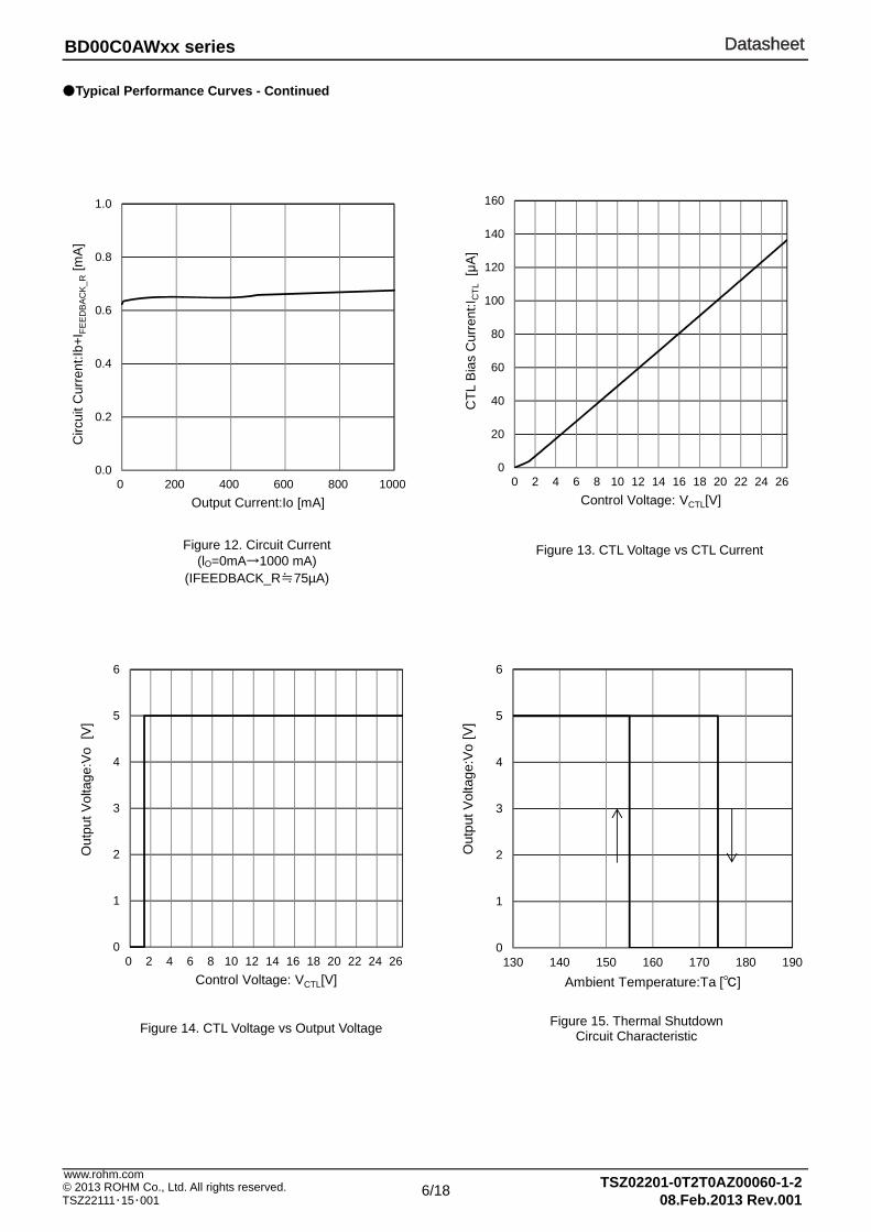
Typical Performance Curves - Continued
Figure 15. Thermal Shutdown Circuit Characteristic Figure 14. CTL Voltage vs Output Voltage
Figure 12. Circuit Current (lO=0mA→1000 mA)
(IFEEDBACK_R≒75µA)
Figure 13. CTL Voltage vs CTL Current
0.0
0.2
0.4
0.6
0.8
1.0
0 200 400 600 800 1000
Circ
uit C
urre
nt:Ib
+IFE
EDBA
CK_
R[m
A]
Output Current:Io [mA]
0
20
40
60
80
100
120
140
160
0 2 4 6 8 10 12 14 16 18 20 22 24 26C
TL B
ias
Cur
rent
:I CTL
[μA]
Control Voltage: VCTL[V]
0
1
2
3
4
5
6
0 2 4 6 8 10 12 14 16 18 20 22 24 26
Out
put V
olta
ge:V
o [V
]
Control Voltage: VCTL[V]
0
1
2
3
4
5
6
130 140 150 160 170 180 190
Out
put V
olta
ge:V
o [V
]
Ambient Temperature:Ta []
DatasheetDatasheet
7/18 TSZ02201-0T2T0AZ00060-1-2© 2013 ROHM Co., Ltd. All rights reserved. TSZ22111・15・001 08.Feb.2013 Rev.001
BD00C0AWxx series
www.rohm.com
A Vcc
CTLGND
Vo
ADJ1µF
5V 10kΩ
56.7kΩ1µF
Measurement Circuit of Fig.1
A
Vcc
CTLGND
Vo
ADJ1µF
56.7kΩ
Vcc
CTLGND
Vo
ADJ1µF
5V
56.7kΩ
Vcc
CTLGND
Vo
ADJ1µF
5V
56.7kΩ
Vcc
CTLGND
Vo
ADJ1µF
5V
56.7kΩ
Vcc
CTLGND
Vo
ADJ1µF
5V
56.7kΩ
Vcc
CTLGND
Vo
ADJ1µF
5V
56.7kΩ
Vcc
CTLGND
Vo
ADJ1µF
5V
56.7kΩ
Vcc
CTLGND
Vo
ADJ1µF
5V
56.7kΩ
Vcc
CTLGND
Vo
ADJ1µF
10V
56.7kΩ
Vcc
CTLGND
Vo
ADJ1µF
10V
56.7kΩ
Vcc
CTLGND
Vo
ADJ1µF
5V
56.7kΩ
V
V
500mA
A A
4.75V
V
~
100mA10V
V10V
A
A
10V
V V
10V
10V
1Vrms
10kΩ
1µF
10kΩ
1µF
10kΩ
1µF
10kΩ
1µF
10kΩ
1µF
10kΩ
1µF
10kΩ
1µF
10kΩ
1µF
10kΩ
1µF
10kΩ
1µF
10kΩ
1µF
IFEEDBACK _R
IFEEDBACK _R
Measurement Circuit of Fig.2 Measurement Circuit of Fig.3
Measurement Circuit of Fig.4 Measurement Circuit of Fig.5 Measurement Circuit of Fig.6
Measurement Circuit of Fig.7 Measurement Circuit of Fig.8 Measurement Circuit of Fig.9
Measurement Circuit of Fig.10 Measurement Circuit of Fig.11 Measurement Circuit of Fig.12
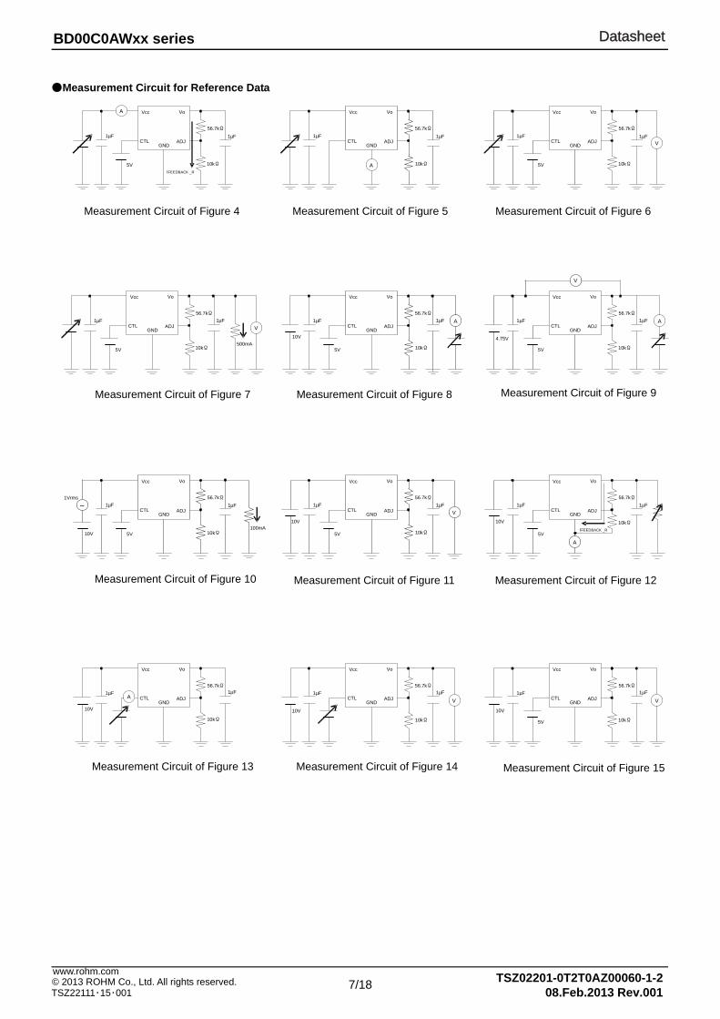
Measurement Circuit for Reference Data
Measurement Circuit of Figure 4 Measurement Circuit of Figure 5 Measurement Circuit of Figure 6
Measurement Circuit of Figure 7 Measurement Circuit of Figure 8 Measurement Circuit of Figure 9
Measurement Circuit of Figure 10 Measurement Circuit of Figure 11 Measurement Circuit of Figure 12
Measurement Circuit of Figure 13 Measurement Circuit of Figure 14 Measurement Circuit of Figure 15
DatasheetDatasheet
8/18 TSZ02201-0T2T0AZ00060-1-2© 2013 ROHM Co., Ltd. All rights reserved. TSZ22111・15・001 08.Feb.2013 Rev.001
BD00C0AWxx series
www.rohm.com
VCC
GND
VCC
GND
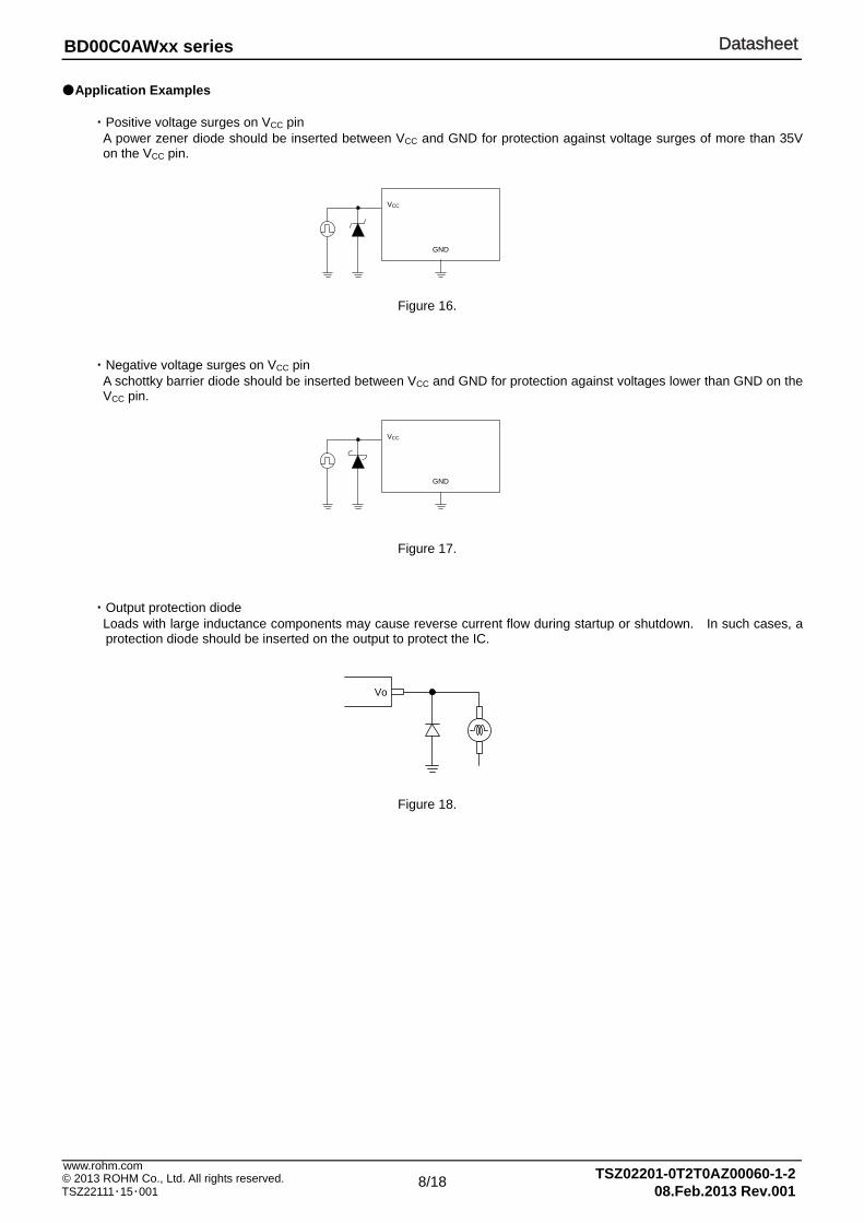
Application Examples ・Positive voltage surges on VCC pin
A power zener diode should be inserted between VCC and GND for protection against voltage surges of more than 35V on the VCC pin.
・Negative voltage surges on VCC pin
A schottky barrier diode should be inserted between VCC and GND for protection against voltages lower than GND on the VCC pin.
・Output protection diode Loads with large inductance components may cause reverse current flow during startup or shutdown. In such cases, a protection diode should be inserted on the output to protect the IC.
Vo
Figure 16.
Figure 17.
Figure 18.
DatasheetDatasheet
9/18 TSZ02201-0T2T0AZ00060-1-2© 2013 ROHM Co., Ltd. All rights reserved. TSZ22111・15・001 08.Feb.2013 Rev.001
BD00C0AWxx series
www.rohm.com
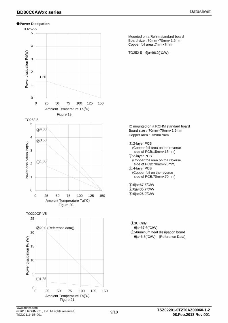
Power Dissipation
Mounted on a Rohm standard board Board size : 70mm×70mm×1.6mm Copper foil area :7mm×7mm TO252-5 θja=96.2(/W)
IC mounted on a ROHM standard board Board size:70mm×70mm×1.6mm Copper area:7mm×7mm ①:2-layer PCB
(Copper foil area on the reverse side of PCB:15mm×15mm)
②:2-layer PCB (Copper foil area on the reverse
side of PCB:70mm×70mm) ③:4-layer PCB
(Copper foil on the reverse side of PCB:70mm×70mm)
①:θja=67.6/W ②:θja=35.7/W ③:θja=26.0/W
①:IC Only θja=67.6(/W)
②:Aluminum heat dissipation board θja=6.3(/W) (Reference Data)
Figure 21.
TO220CP-V5
0
5
10
15
20
25
0 25 50 75 100 125 150Ambient Temperature Ta()
Pow
er d
issi
patio
n P
d (W
)
①1.85
②20.0 (Reference data))
Figure 19.
TO252-5
0
1
2
3
4
5
0 25 50 75 100 125 150Ambient Temperature Ta()
Pow
er d
issi
patio
n P
d(W
)
1.30
Figure 20.
TO252-5
0
1
2
3
4
5
0 25 50 75 100 125 150Ambient Temperature Ta()
Pow
er d
issi
patio
n P
d(W
)
① 1.85
② 3.50
③ 4.80
DatasheetDatasheet
10/18 TSZ02201-0T2T0AZ00060-1-2© 2013 ROHM Co., Ltd. All rights reserved. TSZ22111・15・001 08.Feb.2013 Rev.001
BD00C0AWxx series
www.rohm.com
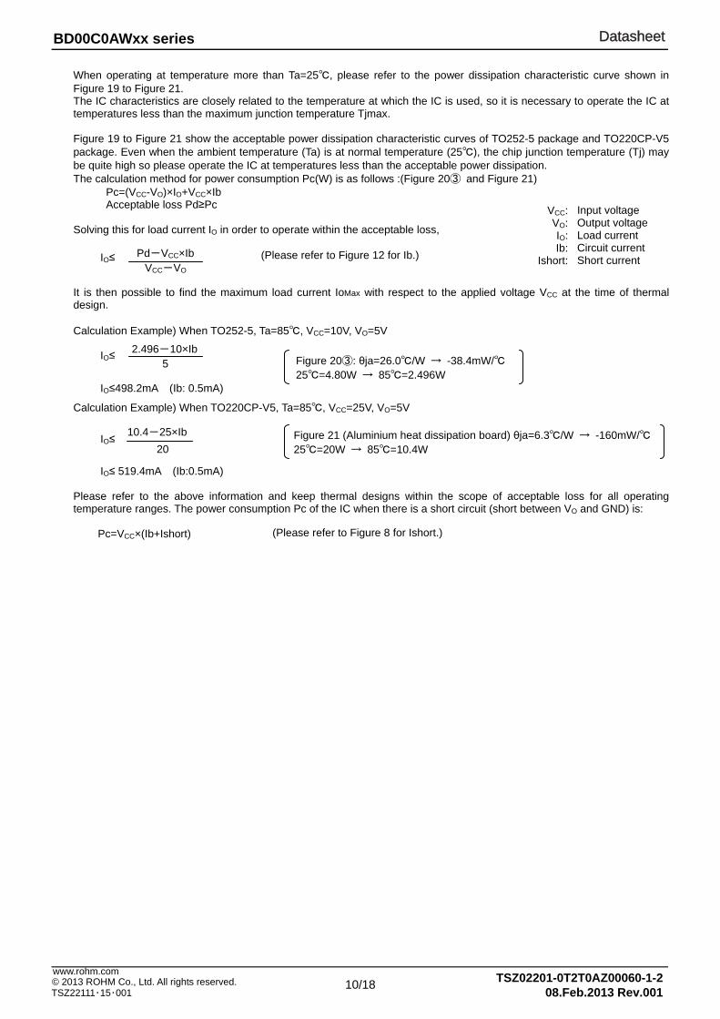
When operating at temperature more than Ta=25, please refer to the power dissipation characteristic curve shown in Figure 19 to Figure 21. The IC characteristics are closely related to the temperature at which the IC is used, so it is necessary to operate the IC at temperatures less than the maximum junction temperature Tjmax. Figure 19 to Figure 21 show the acceptable power dissipation characteristic curves of TO252-5 package and TO220CP-V5 package. Even when the ambient temperature (Ta) is at normal temperature (25), the chip junction temperature (Tj) may be quite high so please operate the IC at temperatures less than the acceptable power dissipation. The calculation method for power consumption Pc(W) is as follows :(Figure 20③ and Figure 21)
Pc=(VCC-VO)×IO+VCC×Ib Acceptable loss Pd≥Pc
Solving this for load current IO in order to operate within the acceptable loss, It is then possible to find the maximum load current IoMax with respect to the applied voltage VCC at the time of thermal design. Calculation Example) When TO252-5, Ta=85, VCC=10V, VO=5V Calculation Example) When TO220CP-V5, Ta=85, VCC=25V, VO=5V Please refer to the above information and keep thermal designs within the scope of acceptable loss for all operating temperature ranges. The power consumption Pc of the IC when there is a short circuit (short between VO and GND) is:
Pc=VCC×(Ib+Ishort)
VCC: VO: IO: Ib:
Ishort:
Input voltage Output voltage Load current Circuit current Short current (Please refer to Figure 12 for Ib.)
(Please refer to Figure 8 for Ishort.)
Figure 20③: θja=26.0/W → -38.4mW/ 25=4.80W → 85=2.496W
IO≤
IO≤498.2mA (Ib: 0.5mA)
2.496-10×Ib 5
IO≤ 10.4-25×Ib 20
Figure 21 (Aluminium heat dissipation board) θja=6.3/W → -160mW/ 25=20W → 85=10.4W
IO≤ 519.4mA (Ib:0.5mA)
IO≤ Pd-VCC×Ib VCC-VO
DatasheetDatasheet
11/18 TSZ02201-0T2T0AZ00060-1-2© 2013 ROHM Co., Ltd. All rights reserved. TSZ22111・15・001 08.Feb.2013 Rev.001
BD00C0AWxx series
www.rohm.com
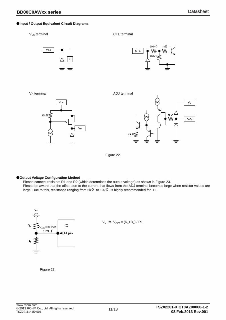
Input / Output Equivalent Circuit Diagrams
Output Voltage Configuration Method Please connect resistors R1 and R2 (which determines the output voltage) as shown in Figure 23. Please be aware that the offset due to the current that flows from the ADJ terminal becomes large when resistor values are large. Due to this, resistance ranging from 5kΩ to 10kΩ is highly recommended for R1.
VO ≒ VADJ × (R1+R2) / R1
Figure 23.
Vcc
IC
CTL
200kΩ
200kΩ
1kΩ
VCC terminal CTL terminal
Vcc
Vo
15kΩ
VO terminal ADJ terminal
VADJ≒0.75V
Figure 22.
DatasheetDatasheet
12/18 TSZ02201-0T2T0AZ00060-1-2© 2013 ROHM Co., Ltd. All rights reserved. TSZ22111・15・001 08.Feb.2013 Rev.001
BD00C0AWxx series
www.rohm.com
Operational Notes 1. Absolute maximum ratings
Exceeding the absolute maximum rating for supply voltage, operating temperature or other parameters can result in damages to or destruction of the chip. In this event it also becomes impossible to determine the cause of the damage (e.g. short circuit, open circuit, etc). Therefore, if any special mode is being considered with values expected to exceed the absolute maximum ratings, implementing physical safety measures, such as adding fuses, should be considered.
2. The electrical characteristics given in this specification may be influenced by conditions such as temperature, supply voltage and external components. Transient characteristics should be sufficiently verified..
3. GND electric potential Keep the GND pin potential at the lowest (minimum) level under any operating condition. Furthermore, ensure that, including the transient, none of the pin’s voltages are less than the GND pin voltage.
4. Ground wiring pattern When both a small-signal GND and a high current GND are present, single-point grounding (at the set standard point) is recommended. This in order to separate the small-signal and high current patterns and to ensure that voltage changes stemming from the wiring resistance and high current do not cause any voltage change in the small-signal GND. Similarly, care must be taken to avoid wiring pattern fluctuations in any connected external component GND.
5. Inter-pin shorting and mounting errors Ensure that when mounting the IC on the PCB the direction and position are correct. Incorrect mounting may result in damaging the IC. Also, shorts caused by dust entering between the output, input and GND pin may result in damaging the IC.
6. Operation Under Strong Electromagnetic Field Operating the IC in the presence of a strong electromagnetic field may cause the IC to malfunction.
7. Inspection using the set board The IC needs to be discharged after each inspection process as, while using the set board for inspection, connecting a capacitor to a low-impedance pin may cause stress to the IC. As a protection from static electricity, ensure that the assembly setup is grounded and take sufficient caution with transportation and storage. Also, make sure to turn off the power supply when connecting and disconnecting the inspection equipment.
8. Power dissipation (Pd) Should by any chance the power dissipation rating be exceeded the rise in temperature of the chip may result in deterioration of the properties of the chip. The absolute maximum rating of the Pd stated in this specification is when the IC is mounted on a 70mm×70mm×1.6mm glass epoxy board. In case of exceeding this absolute maximum rating, increase the board size and copper area to prevent exceeding the Pd rating.
9. Thermal design The power dissipation under actual operating conditions should be taken into consideration and a sufficient margin should be allowed for in the thermal design. On the reverse side of the package this product has an exposed heat pad for improving the heat dissipation. Use both the front and reverse side of the PCB to increase the heat dissipation pattern as far as possible. The amount of heat generated depends on the voltage difference across the input and output, load current, and bias current. Therefore, when actually using the chip, ensure that the generated heat does not exceed the Pd rating.
Tjmax: Maximum junction temperature=150[], Ta: Peripheral temperature [], θja : Thermal resistance of package-ambience[/W], Pd : Package Power dissipation [W], Pc: Power dissipation [W], VCC: Input Voltage, VO: Output Voltage, IO: Load, Ib : Circuit Current Package Power dissipation : Pd (W) = (Tjmax-Ta) / θja Power dissipation : Pc (W) = (VCC-VO) × IO+VCC×Ib
10. VCC pin
Insert a capacitor(VO≥5.0V:capacitor≥1µF, 3.0≤VO<5.0V:capacitor≥2.2µF) between the VCC and GND pins. Choose the capacitance according to the line between the power smoothing circuit and the VCC pin. Selection of the capacitance also depends on the application. Verify the application and allow for sufficient margins in the design. We recommend using a capacitor with excellent voltage and temperature characteristics.
Electric capacitance
Ceramic capacitors, Low ESR capacitor
IC
DatasheetDatasheet
13/18 TSZ02201-0T2T0AZ00060-1-2© 2013 ROHM Co., Ltd. All rights reserved. TSZ22111・15・001 08.Feb.2013 Rev.001
BD00C0AWxx series
www.rohm.com
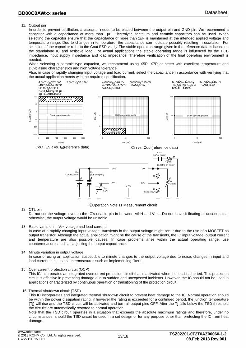
11. Output pin In order to prevent oscillation, a capacitor needs to be placed between the output pin and GND pin. We recommend a capacitor with a capacitance of more than 1μF. Electrolytic, tantalum and ceramic capacitors can be used. When selecting the capacitor ensure that the capacitance of more than 1μF is maintained at the intended applied voltage and temperature range. Due to changes in temperature, the capacitance can fluctuate possibly resulting in oscillation. For selection of the capacitor refer to the Cout ESR vs. IO. The stable operation range given in the reference data is based on the standalone IC and resistive load. For actual applications the stable operating range is influenced by the PCB impedance, input supply impedance and load impedance. Therefore verification of the final operating environment is needed. When selecting a ceramic type capacitor, we recommend using X5R, X7R or better with excellent temperature and DC-biasing characteristics and high voltage tolerance. Also, in case of rapidly changing input voltage and load current, select the capacitance in accordance with verifying that the actual application meets with the required specification.
12. CTL pin Do not set the voltage level on the IC's enable pin in between VthH and VthL. Do not leave it floating or unconnected, otherwise, the output voltage would be unstable.
13. Rapid variation in VCC voltage and load current In case of a rapidly changing input voltage, transients in the output voltage might occur due to the use of a MOSFET as output transistor. Although the actual application might be the cause of the transients, the IC input voltage, output current and temperature are also possible causes. In case problems arise within the actual operating range, use countermeasures such as adjusting the output capacitance.
14. Minute variation in output voltage In case of using an application susceptible to minute changes to the output voltage due to noise, changes in input and load current, etc., use countermeasures such as implementing filters.
15. Over current protection circuit (OCP) This IC incorporates an integrated overcurrent protection circuit that is activated when the load is shorted. This protection circuit is effective in preventing damage due to sudden and unexpected incidents. However, the IC should not be used in applications characterized by continuous operation or transitioning of the protection circuit.
16. Thermal shutdown circuit (TSD) This IC incorporates and integrated thermal shutdown circuit to prevent heat damage to the IC. Normal operation should be within the power dissipation rating, if however the rating is exceeded for a continued period, the junction temperature (Tj) will rise and the TSD circuit will be activated and turn all output pins OFF. After the Tj falls below the TSD threshold the circuits are automatically restored to normal operation. Note that the TSD circuit operates in a situation that exceeds the absolute maximum ratings and therefore, under no circumstances, should the TSD circuit be used in a set design or for any purpose other than protecting the IC from heat damage.
Cout_ESR vs. IO(reference data) Cin vs. Cout(reference data)
※Operation Note 11 Measurement circuit
4.0V≤VCC≤26.5V 3.0V≤VO≤15.0V -40≤Ta≤+105 5kΩ≤R1≤10kΩ 2.2µF≤Cin≤100µF 1µF≤Cout≤100µF
4.0V≤VCC≤26.5V 3.0V≤VO≤15.0V -40≤Ta≤+105 0A≤IO≤1A 5kΩ≤R1≤10kΩ
1
10
100
1 10 100
Cout(µF)
Cin(
µF)
Stable operating region
2.2
Unstable operating region
1
10
100
1 10 100
Cout(μF)
Cin(μ
F)
Stable operating region
6.0V≤VCC≤26.5V 5.0V≤VO≤15.0V -40≤Ta≤+105 0A≤IO≤1A 5kΩ≤R1≤10kΩ
Vcc
CTL
Vo
ADJGND
VCTL(5.0V)
Cin(1µF or higher)
Vcc(4.0V to 26.5V)
R1
(5k to 10kΩ)
R2
Io(Rout)
Cout(1µF or higher)
ESR(0.001Ω or higher)
0.001
0.01
0.1
1
10
100
0 200 400 600 800 1000
Io(mA)
Cout_ESR(Ω
)
Unstable operating region
Stable operating region
DatasheetDatasheet
14/18 TSZ02201-0T2T0AZ00060-1-2© 2013 ROHM Co., Ltd. All rights reserved. TSZ22111・15・001 08.Feb.2013 Rev.001
BD00C0AWxx series
www.rohm.com
17. In some applications, the VCC and pin potential might be reversed, possibly resulting in circuit internal damage or damage
to the elements. For example, while the external capacitor is charged, the VCC shorts to the GND. Use a capacitor with a capacitance with less than 1000μF. We also recommend using reverse polarity diodes in series or a bypass between all pins and the VCC pin.
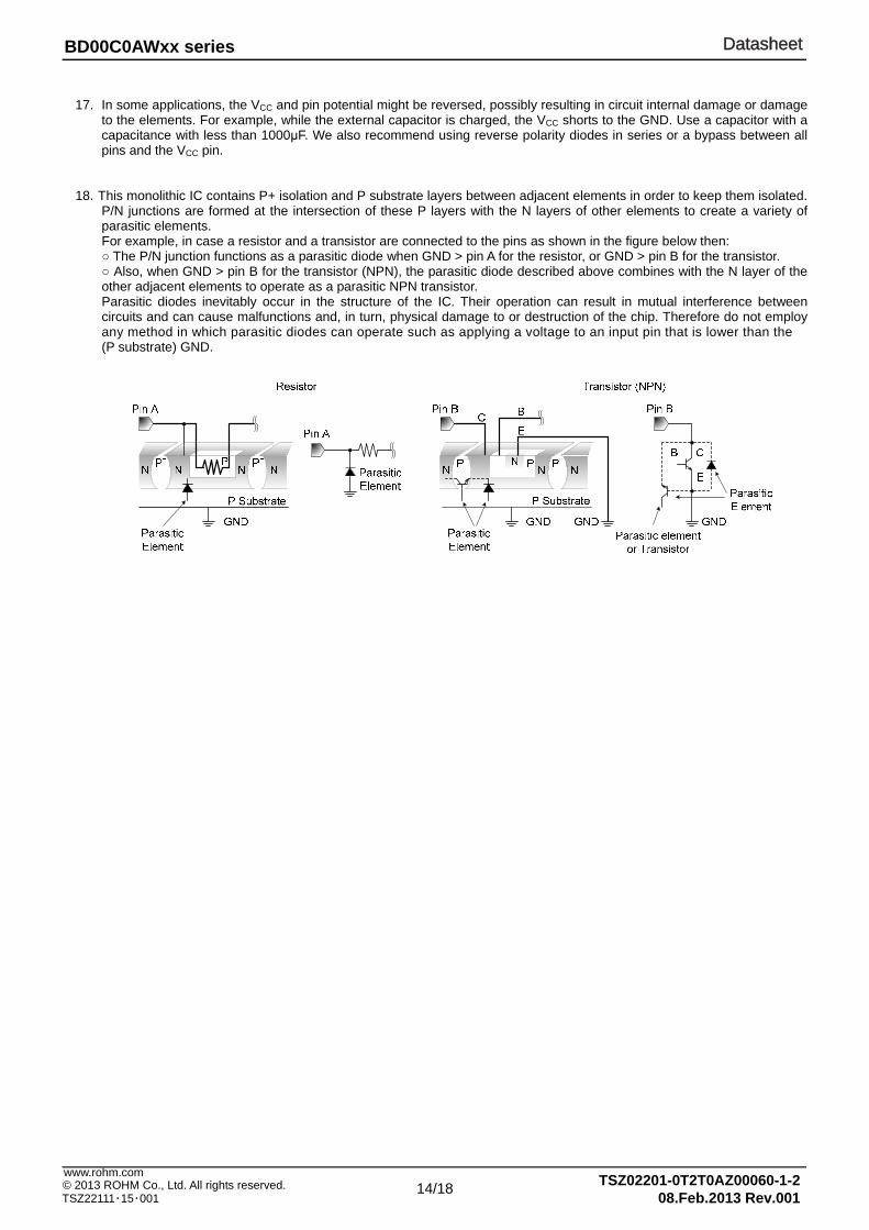
18. This monolithic IC contains P+ isolation and P substrate layers between adjacent elements in order to keep them isolated. P/N junctions are formed at the intersection of these P layers with the N layers of other elements to create a variety of parasitic elements. For example, in case a resistor and a transistor are connected to the pins as shown in the figure below then: The P/N junction functions as a parasitic diode when GND > pin A for the resistor, or GND > pin B for the transistor. Also, when GND > pin B for the transistor (NPN), the parasitic diode described above combines with the N layer of the other adjacent elements to operate as a parasitic NPN transistor. Parasitic diodes inevitably occur in the structure of the IC. Their operation can result in mutual interference between circuits and can cause malfunctions and, in turn, physical damage to or destruction of the chip. Therefore do not employ any method in which parasitic diodes can operate such as applying a voltage to an input pin that is lower than the (P substrate) GND.
DatasheetDatasheet
15/18 TSZ02201-0T2T0AZ00060-1-2© 2013 ROHM Co., Ltd. All rights reserved. TSZ22111・15・001 08.Feb.2013 Rev.001
BD00C0AWxx series
www.rohm.com
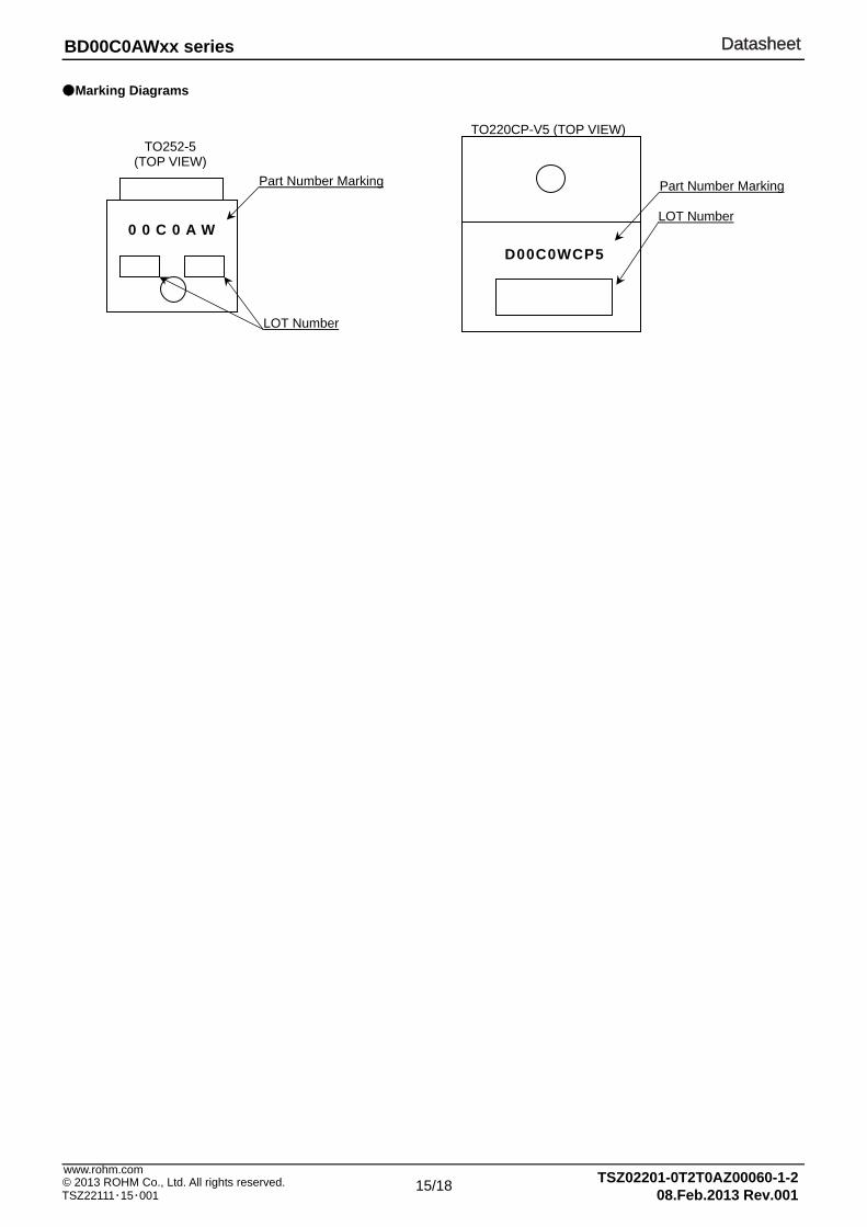
Marking Diagrams
TO252-5 (TOP VIEW)
Part Number Marking
LOT Number
0 0 C 0 A W
TO220CP-V5 (TOP VIEW)
D00C0WCP5
Part Number Marking
LOT Number
DatasheetDatasheet
16/18 TSZ02201-0T2T0AZ00060-1-2© 2013 ROHM Co., Ltd. All rights reserved. TSZ22111・15・001 08.Feb.2013 Rev.001
BD00C0AWxx series
www.rohm.com
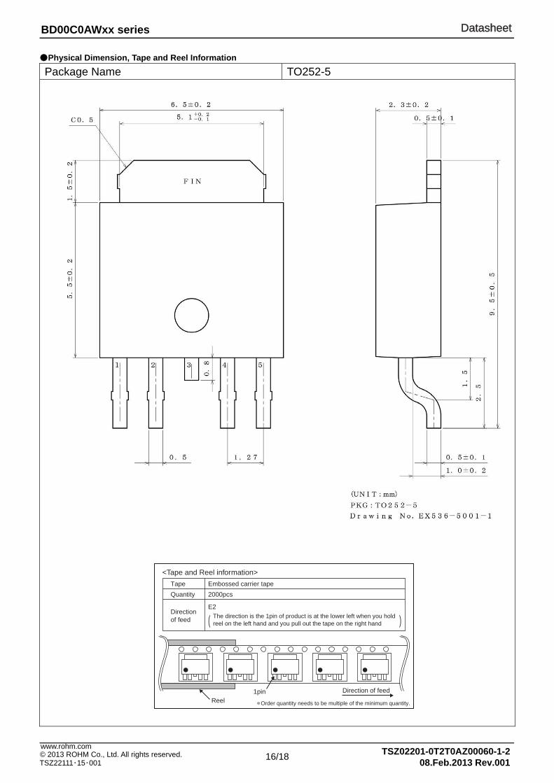
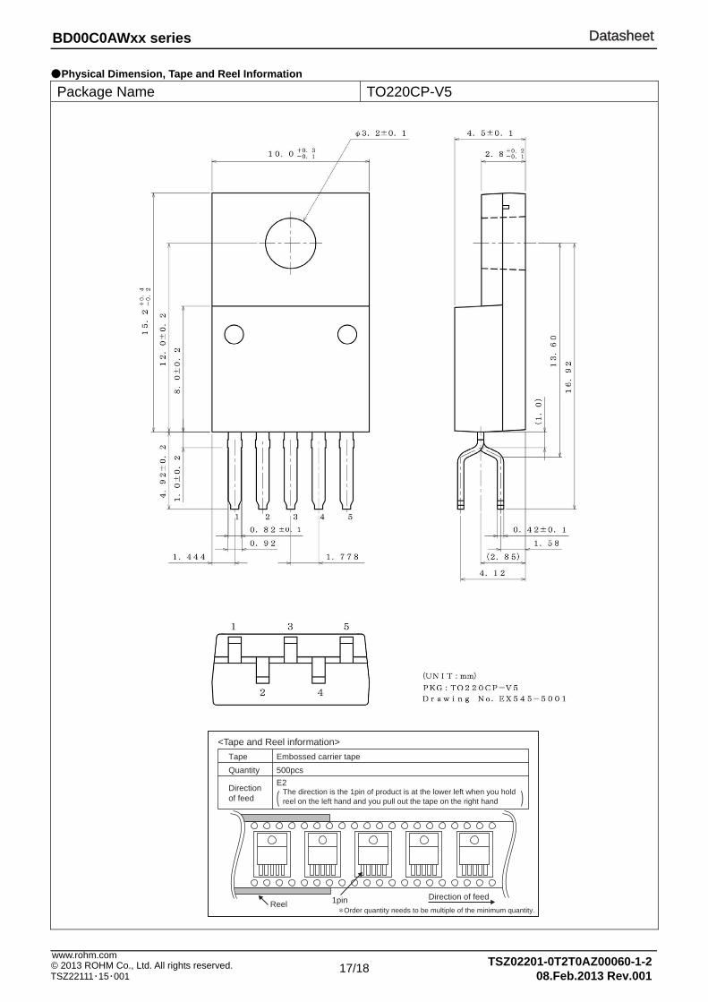
Physical Dimension, Tape and Reel Information
Package Name TO252-5
Direction of feed1pinReel ∗ Order quantity needs to be multiple of the minimum quantity.
<Tape and Reel information>
Embossed carrier tapeTape
Quantity
Direction of feed
The direction is the 1pin of product is at the lower left when you hold reel on the left hand and you pull out the tape on the right hand
2000pcs
E2
( )
DatasheetDatasheet
17/18 TSZ02201-0T2T0AZ00060-1-2© 2013 ROHM Co., Ltd. All rights reserved. TSZ22111・15・001 08.Feb.2013 Rev.001
BD00C0AWxx series
www.rohm.com
Physical Dimension, Tape and Reel Information
Package Name TO220CP-V5
Direction of feed1pinReel∗ Order quantity needs to be multiple of the minimum quantity.
<Tape and Reel information>
Embossed carrier tapeTape
Quantity
Direction of feed
The direction is the 1pin of product is at the lower left when you hold reel on the left hand and you pull out the tape on the right hand
500pcs
E2
( )
DatasheetDatasheet
18/18 TSZ02201-0T2T0AZ00060-1-2© 2013 ROHM Co., Ltd. All rights reserved. TSZ22111・15・001 08.Feb.2013 Rev.001
BD00C0AWxx series
www.rohm.com
Revision History
Date Revision Changes 08.Feb.2013 001 New Release
DatasheetDatasheet
Notice - Rev.004 © 2013 ROHM Co., Ltd. All rights reserved.
Notice General Precaution
1) Before you use our Products, you are requested to carefully read this document and fully understand its contents. ROHM shall not be in any way responsible or liable for failure, malfunction or accident arising from the use of any ROHM’s Products against warning, caution or note contained in this document.
2) All information contained in this document is current as of the issuing date and subject to change without any prior
notice. Before purchasing or using ROHM’s Products, please confirm the latest information with a ROHM sales representative.
Precaution on using ROHM Products
1) Our Products are designed and manufactured for application in ordinary electronic equipments (such as AV equipment, OA equipment, telecommunication equipment, home electronic appliances, amusement equipment, etc.). If you intend to use our Products in devices requiring extremely high reliability (such as medical equipment, transport equipment, traffic equipment, aircraft/spacecraft, nuclear power controllers, fuel controllers, car equipment including car accessories, safety devices, etc.) and whose malfunction or failure may cause loss of human life, bodily injury or serious damage to property (“Specific Applications”), please consult with the ROHM sales representative in advance. Unless otherwise agreed in writing by ROHM in advance, ROHM shall not be in any way responsible or liable for any damages, expenses or losses incurred by you or third parties arising from the use of any ROHM’s Products for Specific Applications.
2) ROHM designs and manufactures its Products subject to strict quality control system. However, semiconductor
products can fail or malfunction at a certain rate. Please be sure to implement, at your own responsibilities, adequate safety measures including but not limited to fail-safe design against the physical injury, damage to any property, which a failure or malfunction of our Products may cause. The following are examples of safety measures:
[a] Installation of protection circuits or other protective devices to improve system safety [b] Installation of redundant circuits to reduce the impact of single or multiple circuit failure
3) Our Products are designed and manufactured for use under standard conditions and not under any special or extraordinary environments or conditions, as exemplified below. Accordingly, ROHM shall not be in any way responsible or liable for any damages, expenses or losses arising from the use of any ROHM’s Products under any special or extraordinary environments or conditions. If you intend to use our Products under any special or extraordinary environments or conditions (as exemplified below), your independent verification and confirmation of product performance, reliability, etc, prior to use, must be necessary:
[a] Use of our Products in any types of liquid, including water, oils, chemicals, and organic solvents [b] Use of our Products outdoors or in places where the Products are exposed to direct sunlight or dust [c] Use of our Products in places where the Products are exposed to sea wind or corrosive gases, including Cl2,
H2S, NH3, SO2, and NO2
[d] Use of our Products in places where the Products are exposed to static electricity or electromagnetic waves [e] Use of our Products in proximity to heat-producing components, plastic cords, or other flammable items [f] Sealing or coating our Products with resin or other coating materials [g] Use of our Products without cleaning residue of flux (even if you use no-clean type fluxes, cleaning residue of
flux is recommended); or Washing our Products by using water or water-soluble cleaning agents for cleaning residue after soldering
[h] Use of the Products in places subject to dew condensation
4) The Products are not subject to radiation-proof design. 5) Please verify and confirm characteristics of the final or mounted products in using the Products. 6) In particular, if a transient load (a large amount of load applied in a short period of time, such as pulse) is applied,
confirmation of performance characteristics after on-board mounting is strongly recommended. Avoid applying power exceeding normal rated power; exceeding the power rating under steady-state loading condition may negatively affect product performance and reliability.
7) De-rate Power Dissipation (Pd) depending on Ambient temperature (Ta). When used in sealed area, confirm the actual
ambient temperature. 8) Confirm that operation temperature is within the specified range described in the product specification. 9) ROHM shall not be in any way responsible or liable for failure induced under deviant condition from what is defined in
this document.
DatasheetDatasheet
Notice - Rev.004 © 2013 ROHM Co., Ltd. All rights reserved.
Precaution for Mounting / Circuit board design 1) When a highly active halogenous (chlorine, bromine, etc.) flux is used, the residue of flux may negatively affect product
performance and reliability. 2) In principle, the reflow soldering method must be used; if flow soldering method is preferred, please consult with the
ROHM representative in advance. For details, please refer to ROHM Mounting specification
Precautions Regarding Application Examples and External Circuits 1) If change is made to the constant of an external circuit, please allow a sufficient margin considering variations of the
characteristics of the Products and external components, including transient characteristics, as well as static characteristics.
2) You agree that application notes, reference designs, and associated data and information contained in this document
are presented only as guidance for Products use. Therefore, in case you use such information, you are solely responsible for it and you must exercise your own independent verification and judgment in the use of such information contained in this document. ROHM shall not be in any way responsible or liable for any damages, expenses or losses incurred by you or third parties arising from the use of such information.
Precaution for Electrostatic
This Product is electrostatic sensitive product, which may be damaged due to electrostatic discharge. Please take proper caution in your manufacturing process and storage so that voltage exceeding the Products maximum rating will not be applied to Products. Please take special care under dry condition (e.g. Grounding of human body / equipment / solder iron, isolation from charged objects, setting of Ionizer, friction prevention and temperature / humidity control).
Precaution for Storage / Transportation 1) Product performance and soldered connections may deteriorate if the Products are stored in the places where:
[a] the Products are exposed to sea winds or corrosive gases, including Cl2, H2S, NH3, SO2, and NO2 [b] the temperature or humidity exceeds those recommended by ROHM [c] the Products are exposed to direct sunshine or condensation [d] the Products are exposed to high Electrostatic
2) Even under ROHM recommended storage condition, solderability of products out of recommended storage time period may be degraded. It is strongly recommended to confirm solderability before using Products of which storage time is exceeding the recommended storage time period.
3) Store / transport cartons in the correct direction, which is indicated on a carton with a symbol. Otherwise bent leads
may occur due to excessive stress applied when dropping of a carton. 4) Use Products within the specified time after opening a humidity barrier bag. Baking is required before using Products of
which storage time is exceeding the recommended storage time period.
Precaution for Product Label QR code printed on ROHM Products label is for ROHM’s internal use only.
Precaution for Disposition When disposing Products please dispose them properly using an authorized industry waste company.
Precaution for Foreign Exchange and Foreign Trade act Since our Products might fall under controlled goods prescribed by the applicable foreign exchange and foreign trade act, please consult with ROHM representative in case of export.
Precaution Regarding Intellectual Property Rights 1) All information and data including but not limited to application example contained in this document is for reference
only. ROHM does not warrant that foregoing information or data will not infringe any intellectual property rights or any other rights of any third party regarding such information or data. ROHM shall not be in any way responsible or liable for infringement of any intellectual property rights or other damages arising from use of such information or data.:
2) No license, expressly or implied, is granted hereby under any intellectual property rights or other rights of ROHM or any
third parties with respect to the information contained in this document.
DatasheetDatasheet
Notice - Rev.004 © 2013 ROHM Co., Ltd. All rights reserved.
Other Precaution 1) The information contained in this document is provided on an “as is” basis and ROHM does not warrant that all
information contained in this document is accurate and/or error-free. ROHM shall not be in any way responsible or liable for any damages, expenses or losses incurred by you or third parties resulting from inaccuracy or errors of or concerning such information.
2) This document may not be reprinted or reproduced, in whole or in part, without prior written consent of ROHM. 3) The Products may not be disassembled, converted, modified, reproduced or otherwise changed without prior written
consent of ROHM. 4) In no event shall you use in any way whatsoever the Products and the related technical information contained in the
Products or this document for any military purposes, including but not limited to, the development of mass-destruction weapons.
5) The proper names of companies or products described in this document are trademarks or registered trademarks of
ROHM, its affiliated companies or third parties.