lecture 19 - single-phase squarewave inverters 19 - single-phase squarewave inverters...other loads...
TRANSCRIPT
ELEC4614 Power Electronics
Lecture 19 - DC-AC converters (Inverters) 1 F. Rahman
Lecture 19 - Single-phase square-wave inverter
1. Introduction
Inverter circuits supply AC voltage or current to a load from a DC supply. A DC source, often obtained from an AC-DC rectifier, is converted into an AC source of some frequency. A uninterruptible AC supply is an example where the 50 Hz AC power output from the inverter replaces the 50 Hz AC mains supply when the latter is lost due to a fault condition. Solar power is sometimes stored in batteries for use at night or when sun light is not available. Most sizeable machines used in the industry are AC motors, so control of these motors is normally by supplying such motors with a sinusoidal AC supply which is variable in magnitude and frequency by the inverter. Naturally commutated inverters, which were discussed earlier, are capable of converting DC into AC but these are based on phase controlled thyristor converters. The existence of an AC supply is crucial to the operation of such inverters since the ac supply system is relied upon in the turning off the switching devices; in other words, such inverters can not operate stand-alone.
There exists a class of inverters, the load commutated inverters, which employ naturally commutated switching devices. In these applications the load itself makes available voltages which can reverse bias the thyristors and turn these off naturally over the range of operation of the load. Examples of such loads are resonant induction heater supplies, overexcited synchronous motors and other loads which operate with a leading power factor.
ELEC4614 Power Electronics
Lecture 19 - DC-AC converters (Inverters) 2 F. Rahman
These inverters can not operate on zero load because its control circuits are synchronized with load voltages.
Notwithstanding the above applications of naturally commutated converters, when AC power is to be supplied from a DC source, it is advantageous to use force or self commutated devices. Such devices include the BJT, GTO, MOSFET and the IGBT. Until the advent of adequately rated gate turn-off devices of the above types, inverter grade thyristors were used for inverter applications. These used forced turn-off circuits, which in turn employed other thyristors to turn off the main thyristor switches in the inverter. These thyristors were much faster than the rectifier grade thyristors. Forced commutated thyristor inverter circuits have now largely been replaced by the gate-turn-off inverter circuits. However, some of the circuit techniques now find renewed interest in resonant inverter circuits. In this section, we will only cover inverter circuits that employ gate-turn-off devices.
Inverters can broadly be classified into Voltage Source (VSI) and Current Source Inverters (CSI). Voltage source inverters are supplied from ideal (or low impedance) DC voltage sources. The DC source can be fixed or variable, with very low source impedance. With such a source, the output AC voltage is determined completely by the DC source voltage and the states of the switching devices in the inverter. This of course assumes that the load current does not become discontinuous. The DC source may be in the form of batteries, generators, solar cells or for large power applications, controlled or

ELEC4614 Power Electronics
Lecture 19 - DC-AC converters (Inverters) 3 F. Rahman
uncontrolled AC-DC rectifier circuits terminated with a C- or LC-filter which offers low impedance path to the lagging components of the load current which must sink into the DC source.
Current source inverters have a stiff DC current supply, usually through a large inductor or a closed-loop controlled current source. The DC source impedance of such inverters is very high. The output AC current is determined completely from the magnitude of the source current and the states of the switching devices used in the inverter. The output AC voltage form such an inverter is determined by the load impedance and the inverter output current.
Figure 19.1
For inverter circuits, the output voltage and current waveforms, vo and io respectively, are assumed to be AC quantities. These are normally stated in terms of their RMS values. Deviations of these waveforms from their fundamental and sinusoidal component are normally expressed in terms of the THD (Total Harmonic Distortion) Factors.
Vd
Id io
vo
VSI, with fixed or variable Vd
Id
Vd io
vo
CSI, with fixed or variable Id
ELEC4614 Power Electronics
Lecture 19 - DC-AC converters (Inverters) 4 F. Rahman
2. Single-Phase, Voltage Source Inverter Circuits
Circuit Topologies
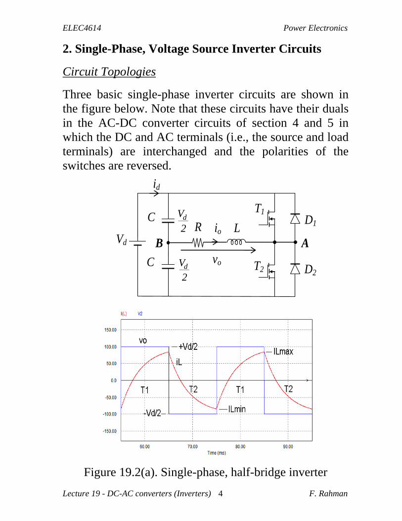
Three basic single-phase inverter circuits are shown in the figure below. Note that these circuits have their duals in the AC-DC converter circuits of section 4 and 5 in which the DC and AC terminals (i.e., the source and load terminals) are interchanged and the polarities of the switches are reversed.
Figure 19.2(a). Single-phase, half-bridge inverter
id
C
C
R LioVd
T1
T2
D1
D2
B A
vo
dV
2
dV
2
ELEC4614 Power Electronics
Lecture 19 - DC-AC converters (Inverters) 5 F. Rahman
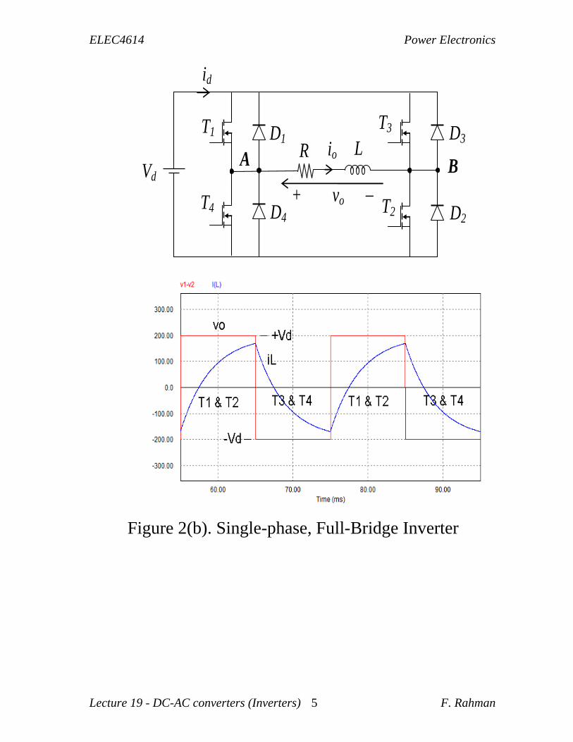
Figure 2(b). Single-phase, Full-Bridge Inverter
id
R LioA
T3
T2
D3
D2
B
+ vo
T1
T4
D1
D4
Vd
ELEC4614 Power Electronics
Lecture 19 - DC-AC converters (Inverters) 6 F. Rahman
D2
v1
Vd
N1
v1
T1 T2
R
+
vL
–
N2
iL
v2
N1
L
D1
Id
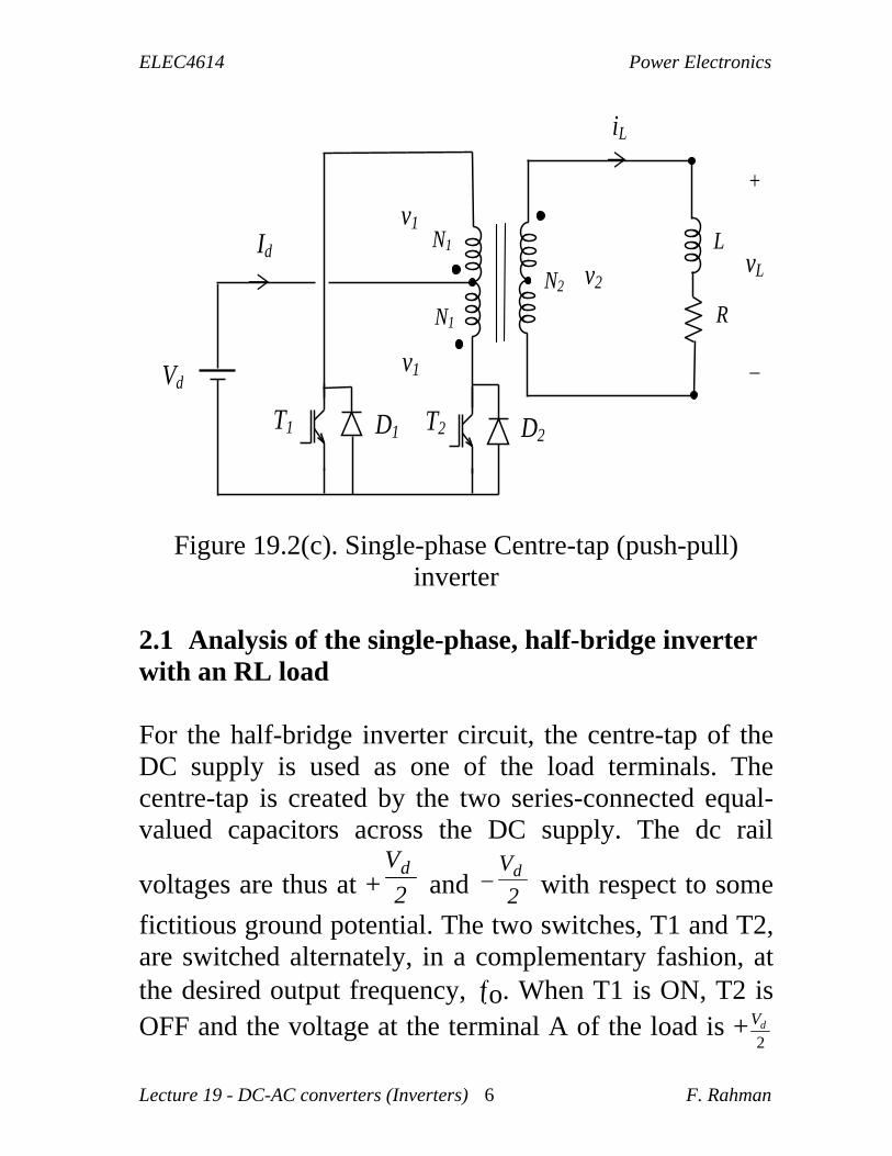
Figure 19.2(c). Single-phase Centre-tap (push-pull) inverter
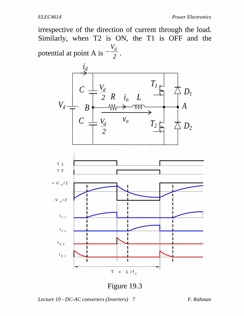
2.1 Analysis of the single-phase, half-bridge inverter with an RL load For the half-bridge inverter circuit, the centre-tap of the DC supply is used as one of the load terminals. The centre-tap is created by the two series-connected equal-valued capacitors across the DC supply. The dc rail
voltages are thus at +Vd
2 and Vd
2 with respect to some
fictitious ground potential. The two switches, T1 and T2, are switched alternately, in a complementary fashion, at the desired output frequency, o. When T1 is ON, T2 is OFF and the voltage at the terminal A of the load is +
2dV
ELEC4614 Power Electronics
Lecture 19 - DC-AC converters (Inverters) 7 F. Rahman
irrespective of the direction of current through the load. Similarly, when T2 is ON, the T1 is OFF and the
potential at point A is dV
2 .
Figure 19.3
id
C
C
R LioVd
T1
T2
D1
D2
B A
vo
dV
2
dV
2
T 1
T 2
+ V d / 2
- V d / 2
I T 1
I T 2
I D 1
I D 2
T = 1 / f o
ELEC4614 Power Electronics
Lecture 19 - DC-AC converters (Inverters) 8 F. Rahman
The load voltage is a square-wave of amplitude Vd/2 and the load current waveform is exponentially rising and falling waveform determined by the load impedance. For a resistive load the current waveform follows the voltage waveform. For an inductive load the current waveform lags the voltage waveform by an angle which is, approximately, the load power factor angle.
When the switch T1 is switched off, the load current is at its positive peak, and it will continue to flow through the diode D2 back into the lower capacitor across the DC source. The conducting diode D2 will reverse bias the transistor T2 (from collector to emitter) until the load current falls to zero. Thereafter, the transistor T2 will be forward biased and negative current will establish in the load through T2. Similarly, diode D1 conducts when T2 is switched OFF and T1 starts to conduct when the load current rises to zero.
Diodes D1 and D2 carry currents which are due to the trapped energy in the load inductor (or the reactive power in the load). Consequently, these diodes are referred to as reactive feedback diodes which return the load reactive power back to the DC source. These diodes are also necessary to allow a path for the current to flow when a transistor is turned off, thus protecting the switches against the overvoltage that would be created by a sudden turn-off of current in the load inductance.
The total RMS value of the load output voltage is given by,

ELEC4614 Power Electronics
Lecture 19 - DC-AC converters (Inverters) 9 F. Rahman
2/ 2
0
2
2 2
Td d
oV V
V dtT
(19.1)
and
1,3,5,
1,3,5,...
14
2 sin sin2
2sin
d
o
n
d
n
V nv n t
n
Vn t
n
(19.2)
The fundamental RMS output voltage is
dd V
VV 45.0
21
(19.3)
The total harmonic distortion of the output voltage is
THD 2
1 3,5,7,
1n
n
VV
= 48.2% (19.4)

ELEC4614 Power Electronics
Lecture 19 - DC-AC converters (Inverters) 10 F. Rahman
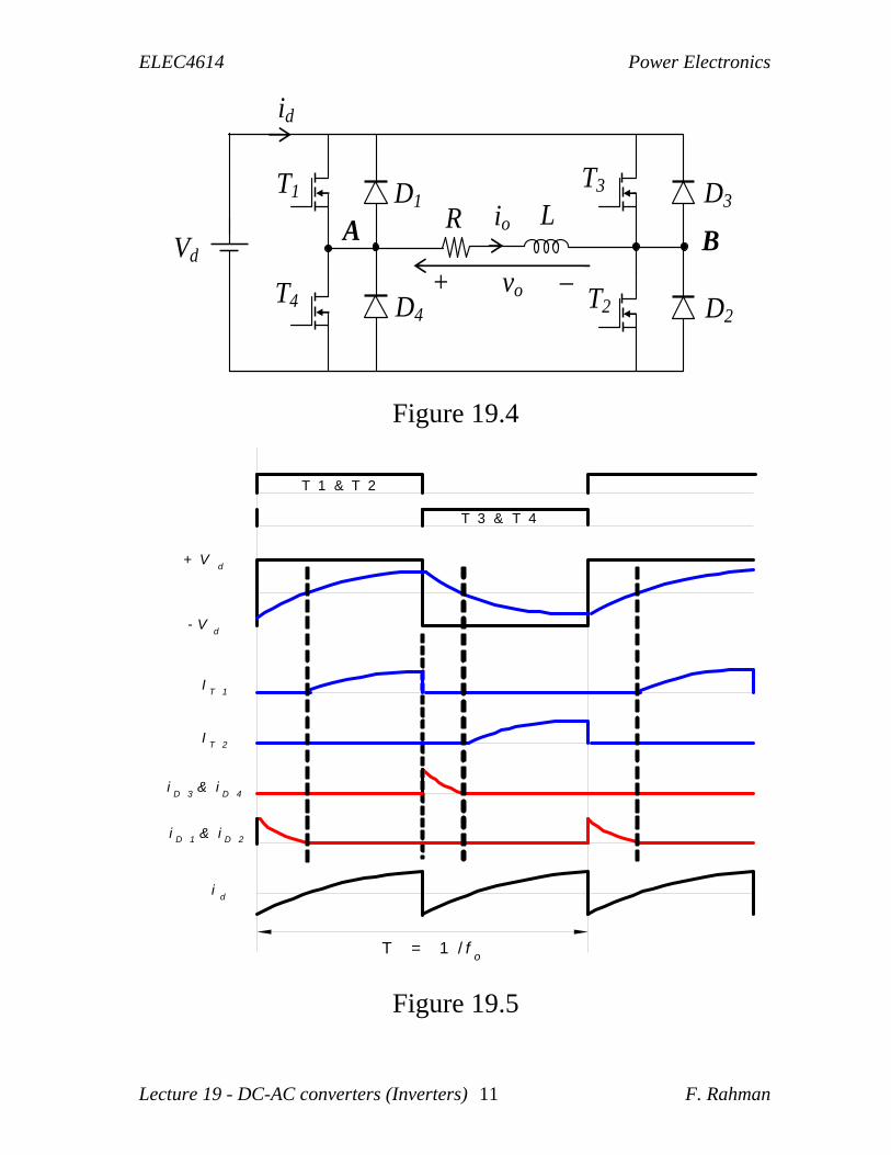
2.2 Analysis of the single-phase full-bridge inverter with RL load
In this circuit four switches are used and the DC supply centre-tap is not required. Switches T1 and T2 are switched together while switches T3 and T4 are switched together alternately to T1 and T2 in a complementary manner. The four feedback diodes D1-D4 conduct currents as indicated in the figure below.
ELEC4614 Power Electronics
Lecture 19 - DC-AC converters (Inverters) 11 F. Rahman
Figure 19.4
T 1 & T 2
T 3 & T 4
+ Vd
- Vd
IT 1
IT 2
i D 1 & i D 2
iD 3
& iD 4
T = 1 / fo
id
Figure 19.5
id
R LioA
T3
T2
D3
D2
B
+ vo
T1
T4
D1
D4
Vd
ELEC4614 Power Electronics
Lecture 19 - DC-AC converters (Inverters) 12 F. Rahman
The output load voltage alternates between +Vd when T1 and T2 are on and -Vd when T3 and T4 are on, irrespective of the direction of current flow. It is assumed that the load current does not become discontinuous at any time. In the following analysis we assume that the load current does not become discontinuous at any time, same as for the half-bridge circuit.
The output RMS voltage
/ 2
2
0
2 T
o d dV V dt VT
(19.5)
1,3,5,
4sind
o
n
Vv n t
n
(19.6)
The fundamental RMS output voltage
dd V
VV 9.0
2
41
(19.7)
When the switches T1 and T2 are on, load current increases exponentially according to
ddi
V L Ridt
(19.8)
Solving this,
i AeV
R
R
Lt
d
(19.9)
ELEC4614 Power Electronics
Lecture 19 - DC-AC converters (Inverters) 13 F. Rahman
Assuming that at t = 0, the initial current is Io, the solution for i is
t
L
R
do
d eR
VI
RV
i
(19.10)
where 0 t t1, t1 being the end of the on period for T1 and T2
At the end of the on period for T1 and T2, io is at maximum, and diodes D3 and D4 start conduction. T3 and T4, though on, are now reverse biased by these diodes. The load current now falls according to
V Ldi
dtRid (19.11)
The solution of this equation is
2
1
Rt
d d LV Vi I e
R R
(19.12)
where 0 t2 t2 – t1, t2 being zero at t1, and I1 is the current at the end of the ON period of T1 and T2.
In the steady-state, I1 = Io. The steady-state value of I1 can be found by solving (10) and (12) simultaneously. I1 in closed form, given by,
ELEC4614 Power Electronics
Lecture 19 - DC-AC converters (Inverters) 14 F. Rahman
1
1
1
1
1
Rt
L
d
Rt
L
eV
IR
e
(19.13)
The zero current cross-over point tx is found from (10) from the condition that at t = tx, i = 0. This gives
tL
R
R
VIx
do
ln 1 sec. (19.14)
The steady-state mean output power to the load is given by
1
1
1 t
do
P V i dtt
watts. (19.15)
where i is found from equations 19.10 or 19.12 in which I1 (or Io ) is given by 19.13.
Note that the transistor and diode currents can be found from the complete solution of i. This is indicated by the waveforms in the figure given above. The ratings of these devices can be found thereon.

ELEC4614 Power Electronics
Lecture 19 - DC-AC converters (Inverters) 15 F. Rahman
2.3 Analysis of the square-wave, centre-tap (push-pull) inverter with R-L load.
In this inverter, the positive terminal of the DC source is connected to the center-tap of a two-winding transformer. The ends of the two primary windings of the primary are connected alternately to the DC supply by switching T1 and T2, producing at the secondary a square-wave voltage. The feedback diodes carry the load current (referred to the primary by the turns-ratio) which flows back into the DC source when a switch is turned off.
Figure 19.6
The secondary (load) voltage is given by
2
1
do
N Vv
N during the +ve half-cycle (19.16)
or 2
1
do
N Vv
N during the –ve half-cycle (19.17)
v1
Vd
R
+ vo
D2
N1:N2
v1
D1
iL
L
T1 T2
id iL
id
2
1
dN V
N
2
1
dN V
N
vo
ELEC4614 Power Electronics
Lecture 19 - DC-AC converters (Inverters) 16 F. Rahman
according to whether switch T1 or T2 are ON, where 2
1
N
N is the turns-ratio between each half of the primary
and the secondary windings. The load current iL is determined by vo and the load impedance as in the previous section. For an inductive load, the secondary current will remain negative for a while after T1 has been switched ON, before becoming positive, when it flows through switch T1. Until then, the referred primary current flows through D1.
Note that in the previous half-cycle, the referred load current was carried through T2. When T2 is turned OFF and T1 is turned on, the primary winding current through T2 immediately transfers to top half of the primary winding and continues to flows through D1 back to the DC source. The same happens when T1 is turned OFF and T2 is turned ON at the end of the ON period for T1.
The primary winding current through T1 and upper half of the primary winding then immediately transfers to D2 and the lower half of the primary winding. Thus, when a switch is turned off, the current in the transformer primary current immediately transfers to the other half of the primary winding. Note that secondary or the load voltage is determined entirely by the switching waveforms, regardless of the devices which carry the referred primary current, assuming that the load current is continuous at all times.
ELEC4614 Power Electronics
Lecture 19 - DC-AC converters (Inverters) 17 F. Rahman
(This instantaneous transfer of current from one part of an inductive circuit to another should not be confused with the notion that current can not change instantaneously in an inductive circuit. It is the magnetic field (which is associated with energy storage) in a magnetic circuit that can not reverse or change instantaneously, not the current).
However, the two halves of the transformer or the switching duration of each switch in each half-cycle (i.e., Ton of each switch) may not be perfectly balanced. Furthermore, the transformer leakage inductance will have some stored energy associated with it. The former will present a DC saturation problem and the stored energy in the leakage inductance will need to be dissipated twice each switching cycle. The former calls for very good coupling between the two windings and the balancing of Ton of each switch, while the latter calls for additional snubber circuits for each switch. These are the main draw backs for the push-pull inverter.
Notwithstanding these, this inverter presents only one device voltage drop between the source and load, compared with two device drops for the full-bridge inverter. Furthermore, the gate drive signals for both switches can be referenced to common ground, which allows simpler driver circuits.
Note that the transformer isolates the DC source circuit from the load. Note also that the peak voltage across a transistor in this circuit is twice the supply voltage.
ELEC4614 Power Electronics
Lecture 19 - DC-AC converters (Inverters) 18 F. Rahman
3. Output voltage control of single-phase inverter
Inverters with fixed output voltage and frequency are normally used for fixed AC power supplies, such as uninterruptible power supplies for computer installations. [But these circuits also have voltage control circuitry to overcome variations in the input DC voltage and load, by closed loop control. The output voltage of these inverter circuits are normally regulated very tightly.]. For other applications such as in variable speed drives, variable output voltage at variable frequency are often required. While frequency control is readily obtained, voltage control requires more elaborate techniques.
Methods employed for voltage control are:
Input voltage regulation - rarely used for voltage- source inverters
Phase control of inverter groups Multiple Pulse Width Modulation Sinusoidal PWM (SPWM) - bilpolar switched Modified SPWM Unipolar switched SPWM
ELEC4614 Power Electronics
Lecture 19 - DC-AC converters (Inverters) 19 F. Rahman
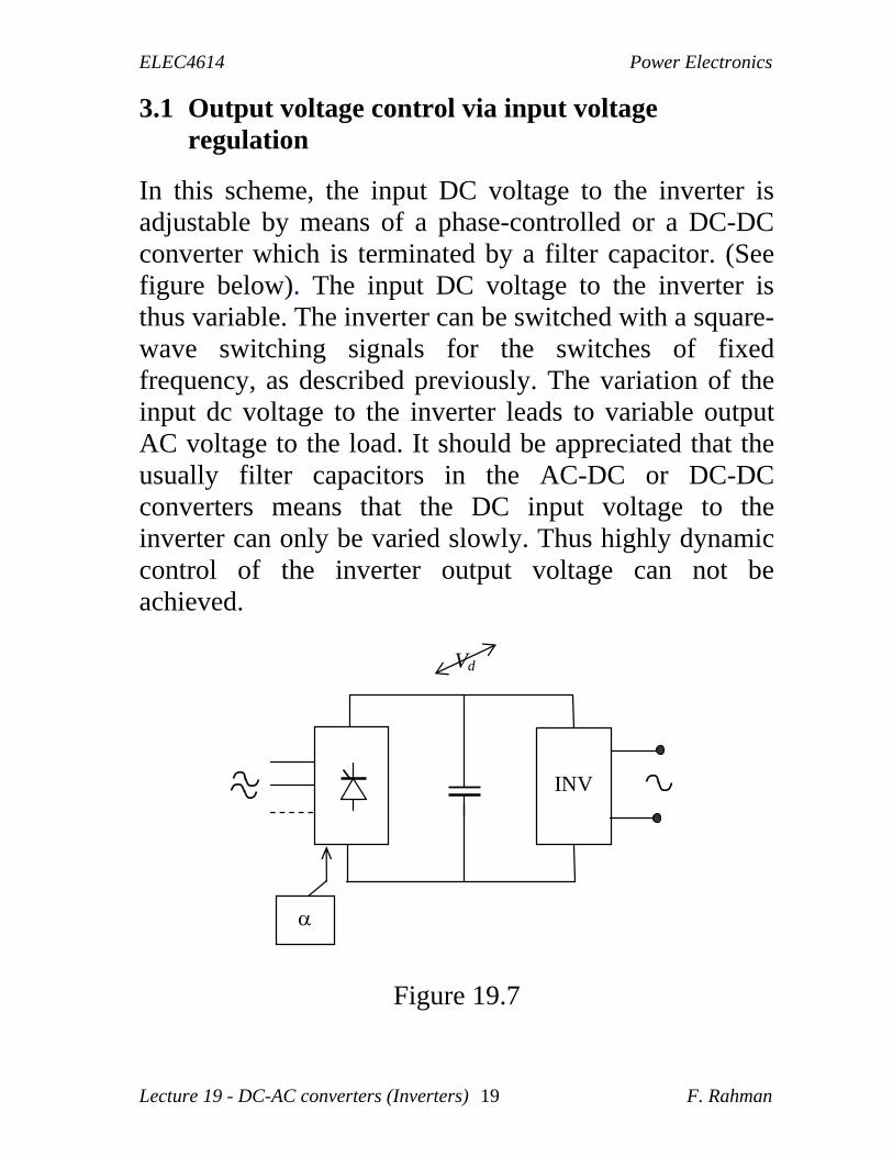
3.1 Output voltage control via input voltage regulation
In this scheme, the input DC voltage to the inverter is adjustable by means of a phase-controlled or a DC-DC converter which is terminated by a filter capacitor. (See figure below). The input DC voltage to the inverter is thus variable. The inverter can be switched with a square-wave switching signals for the switches of fixed frequency, as described previously. The variation of the input dc voltage to the inverter leads to variable output AC voltage to the load. It should be appreciated that the usually filter capacitors in the AC-DC or DC-DC converters means that the DC input voltage to the inverter can only be varied slowly. Thus highly dynamic control of the inverter output voltage can not be achieved.
INV
Vd
Figure 19.7
ELEC4614 Power Electronics
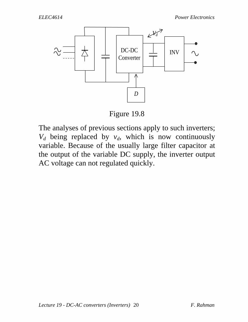
Lecture 19 - DC-AC converters (Inverters) 20 F. Rahman
INV
DC-DC
Converter
D
Vd
Figure 19.8
The analyses of previous sections apply to such inverters; Vd being replaced by vd, which is now continuously variable. Because of the usually large filter capacitor at the output of the variable DC supply, the inverter output AC voltage can not regulated quickly.
ELEC4614 Power Electronics
Lecture 19 - DC-AC converters (Inverters) 21 F. Rahman
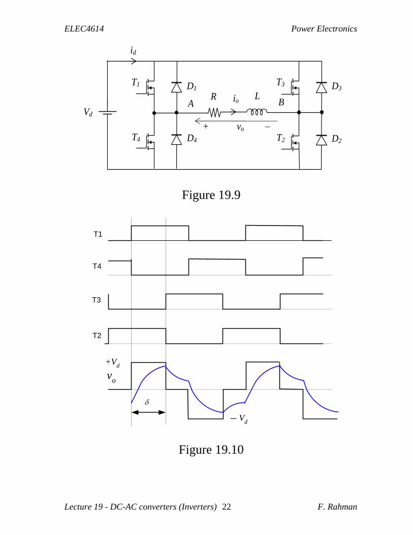
3.2 Phase control of inverter legs
The switching signals of the two inverter legs of a single-phase bridge inverter can be given a variable phase shift angle , as indicated in the figure below. This has the effect of varying the duty cycle of the output voltage in each half cycle, producing a quasi-square output AC voltage waveform, as is also shown in this figure. (Note that each inverter leg has complementary switching). The phase angle is directly proportional to the duration of the non zero output voltage, so that the phase angle can be controlled to vary the output voltage.
ELEC4614 Power Electronics
Lecture 19 - DC-AC converters (Inverters) 22 F. Rahman
id
R L io A
T3
T2
D3
D2
B
+ vo
T1
T4
D1
D4
Vd
Figure 19.9
T1
T4
T3
T2
+Vd
- Vd
vo
Figure 19.10
ELEC4614 Power Electronics
Lecture 19 - DC-AC converters (Inverters) 23 F. Rahman
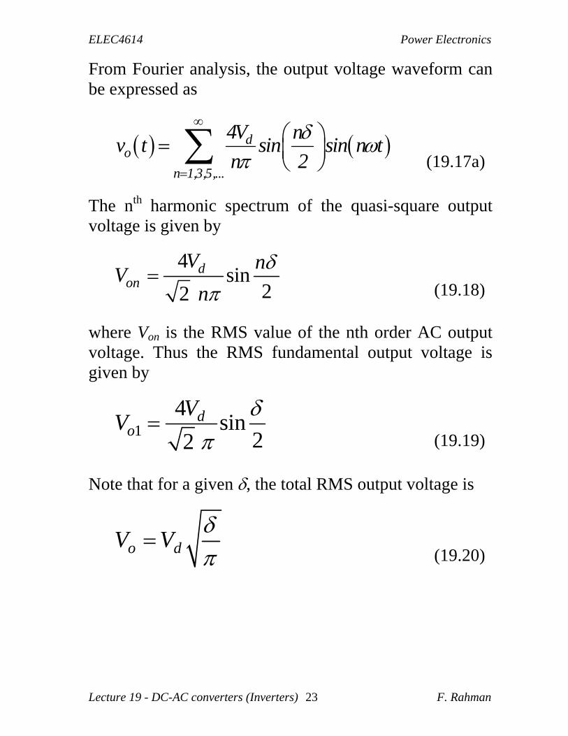
From Fourier analysis, the output voltage waveform can be expressed as
d
o
n 1,3,5,...
4V nv t sin sin n t
n 2
(19.17a)
The nth harmonic spectrum of the quasi-square output voltage is given by
4sin
22d
on
V nV
n
(19.18)
where Von is the RMS value of the nth order AC output voltage. Thus the RMS fundamental output voltage is given by
1
4sin
22d
oV
V
(19.19)
Note that for a given , the total RMS output voltage is
o dV V
(19.20)
ELEC4614 Power Electronics
Lecture 19 - DC-AC converters (Inverters) 24 F. Rahman
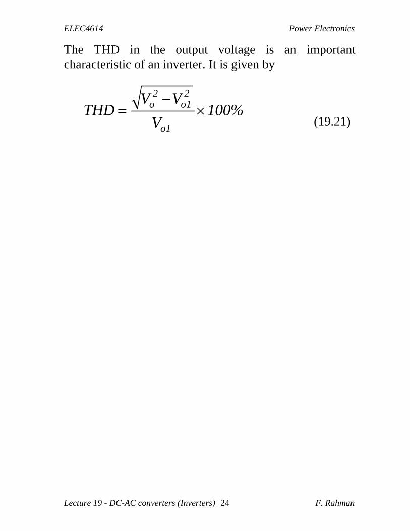
The THD in the output voltage is an important characteristic of an inverter. It is given by
2 2o o1
o1
V VTHD 100%
V
(19.21)