lecture 6 look -up -table (lut) - kdu university...
TRANSCRIPT

Lecture 6
Look-up-table (LUT)
1
Look-up-table (LUT)
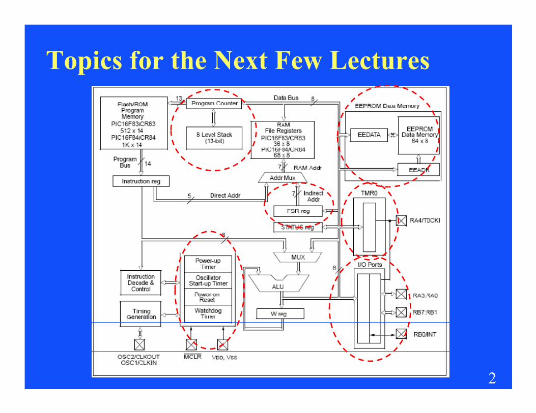
Topics for the Next Few Lectures
2

3
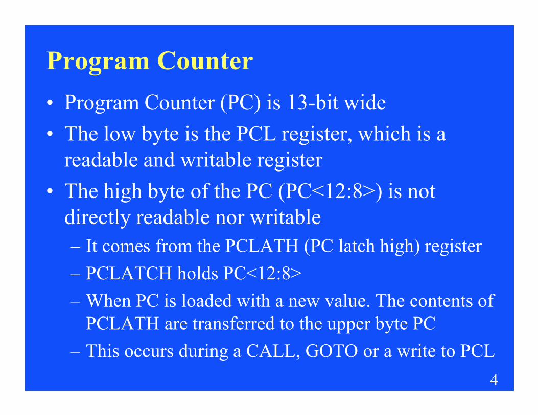
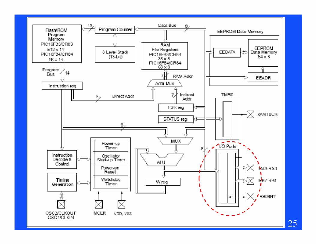
Program Counter
• Program Counter (PC) is 13-bit wide
• The low byte is the PCL register, which is a
readable and writable register
• The high byte of the PC (PC<12:8>) is not
directly readable nor writable
4
directly readable nor writable
– It comes from the PCLATH (PC latch high) register
– PCLATCH holds PC<12:8>
– When PC is loaded with a new value. The contents of
PCLATH are transferred to the upper byte PC
– This occurs during a CALL, GOTO or a write to PCL
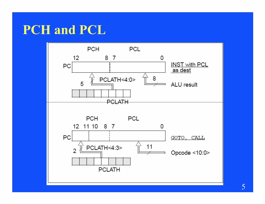
PCH and PCL
5
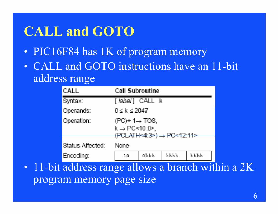
CALL and GOTO
• PIC16F84 has 1K of program memory
• CALL and GOTO instructions have an 11-bit address range
6
• 11-bit address range allows a branch within a 2K program memory page size
CALL and GOTO
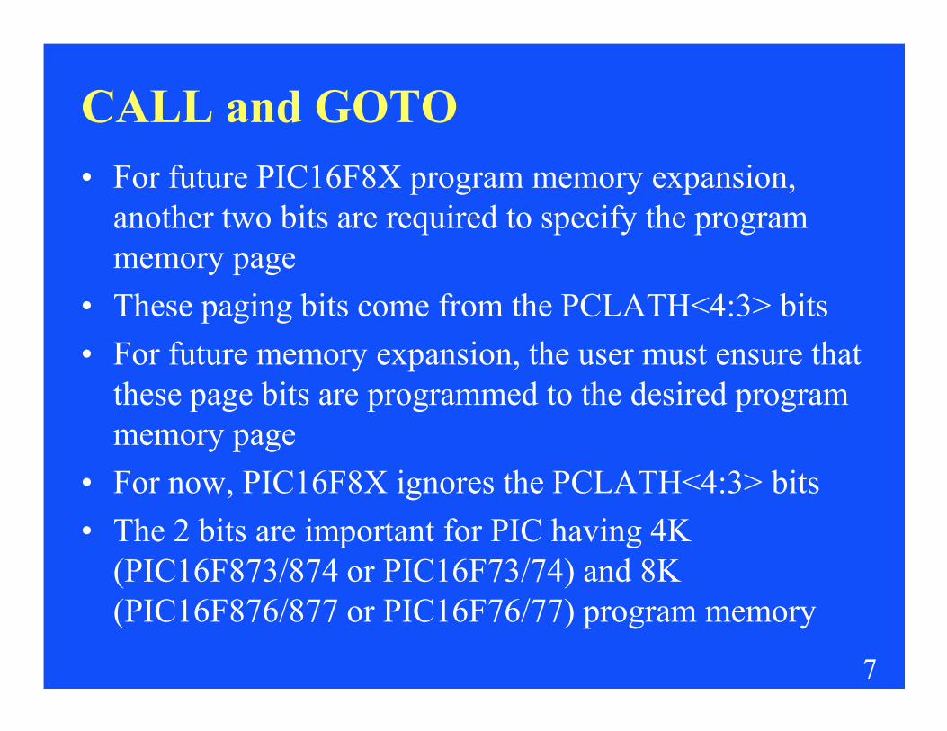
• For future PIC16F8X program memory expansion,
another two bits are required to specify the program
memory page
• These paging bits come from the PCLATH<4:3> bits
• For future memory expansion, the user must ensure that
7
• For future memory expansion, the user must ensure that
these page bits are programmed to the desired program
memory page
• For now, PIC16F8X ignores the PCLATH<4:3> bits
• The 2 bits are important for PIC having 4K
(PIC16F873/874 or PIC16F73/74) and 8K
(PIC16F876/877 or PIC16F76/77) program memory
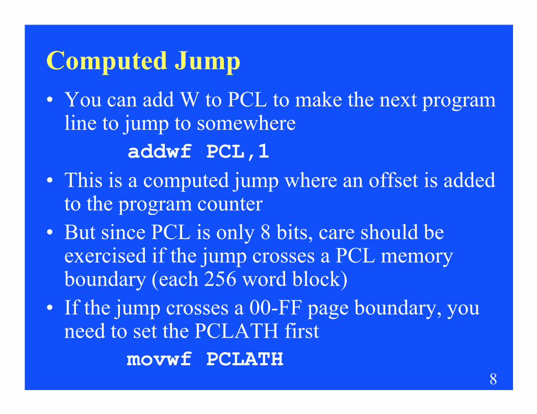
Computed Jump
• You can add W to PCL to make the next program line to jump to somewhere
addwf PCL,1
• This is a computed jump where an offset is added to the program counter
8
to the program counter
• But since PCL is only 8 bits, care should be exercised if the jump crosses a PCL memory boundary (each 256 word block)
• If the jump crosses a 00-FF page boundary, you need to set the PCLATH first
movwf PCLATH
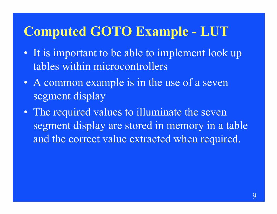
Computed GOTO Example - LUT
• It is important to be able to implement look up
tables within microcontrollers
• A common example is in the use of a seven
segment display
• The required values to illuminate the seven
9
• The required values to illuminate the seven
segment display are stored in memory in a table
and the correct value extracted when required.
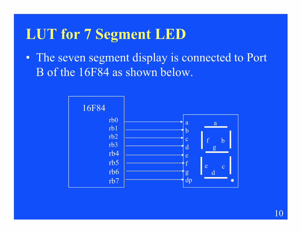
LUT for 7 Segment LED
• The seven segment display is connected to Port
B of the 16F84 as shown below.
rb0
16F84
10
rb0
rb1
rb2
rb3
rb4
rb5
rb6
rb7
a
b
c
d
e
f
g
dp
a
b
cd
e
fg
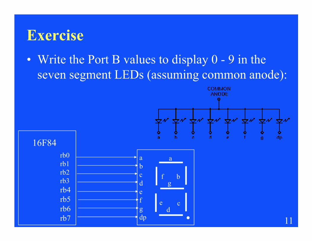
Exercise
• Write the Port B values to display 0 - 9 in the
seven segment LEDs (assuming common anode):
11
rb0
rb1
rb2
rb3
rb4
rb5
rb6
rb7
a
b
c
d
e
f
g
dp
a
b
cd
e
fg
16F84
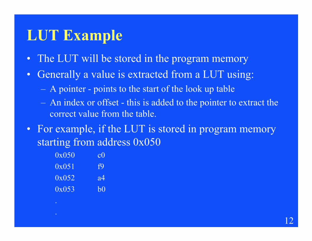
LUT Example
• The LUT will be stored in the program memory
• Generally a value is extracted from a LUT using:
– A pointer - points to the start of the look up table
– An index or offset - this is added to the pointer to extract the
correct value from the table.
12
• For example, if the LUT is stored in program memory
starting from address 0x0500x050 c0
0x051 f9
0x052 a4
0x053 b0
.
.

LUT Example
• To display 3 in the LEDs,
– First set up the pointer to point to the start of the table i.e.
0x050.
– Then set up the index 0x03
• PIC microcontrollers handles LUT in an unusual manner
in that the LUT is called up as a subroutine
13
in that the LUT is called up as a subroutine
• The pointer is the program counter itself
• The index is a value in the w register which is added to
the program counter
• The value is extracted using retlw - return from
subroutine with literal value in w
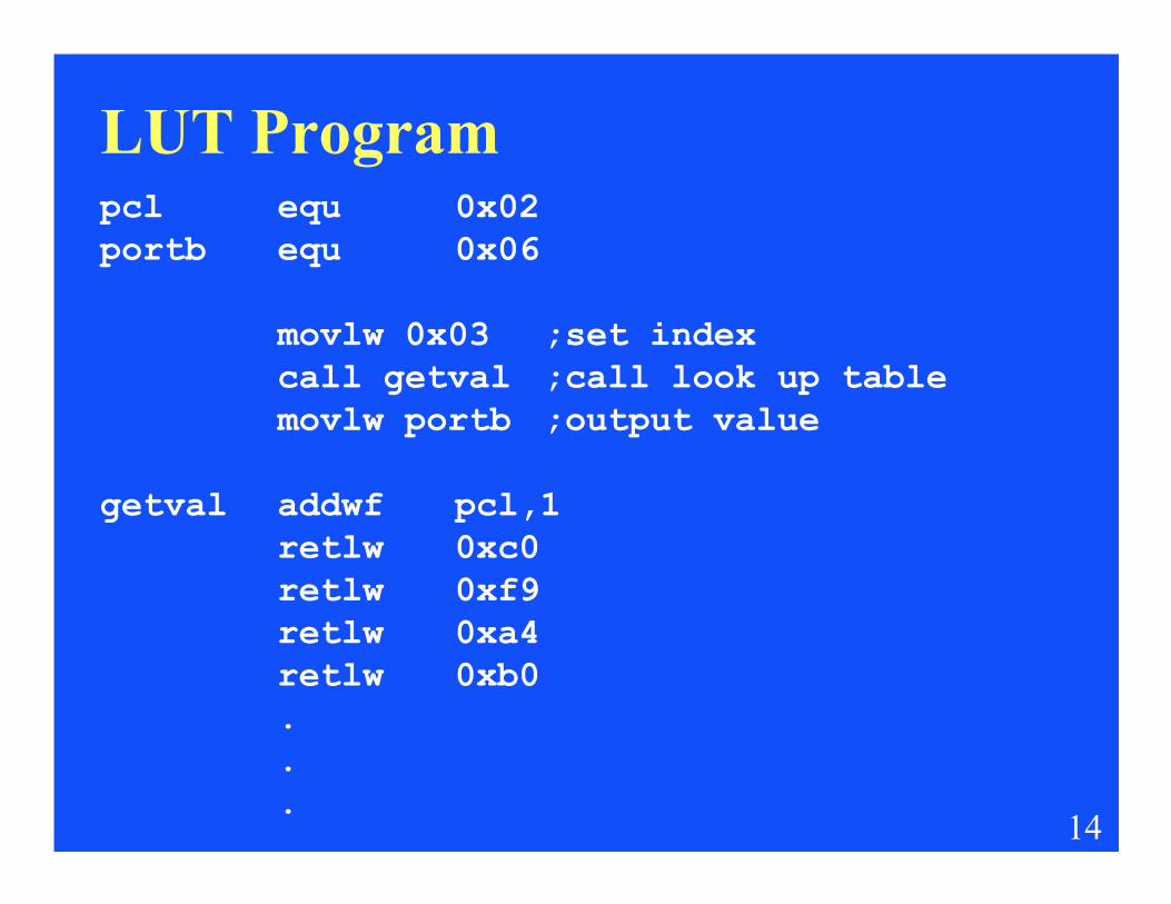
LUT Programpcl equ 0x02
portb equ 0x06
movlw 0x03 ;set index
call getval ;call look up table
movlw portb ;output value
14
getval addwf pcl,1
retlw 0xc0
retlw 0xf9
retlw 0xa4
retlw 0xb0
.
.
.
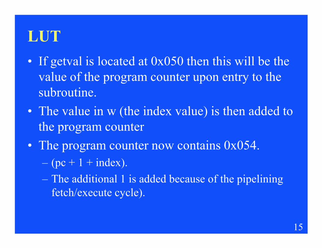
LUT
• If getval is located at 0x050 then this will be the
value of the program counter upon entry to the
subroutine.
• The value in w (the index value) is then added to
the program counter
15
the program counter
• The program counter now contains 0x054.
– (pc + 1 + index).
– The additional 1 is added because of the pipelining
fetch/execute cycle).
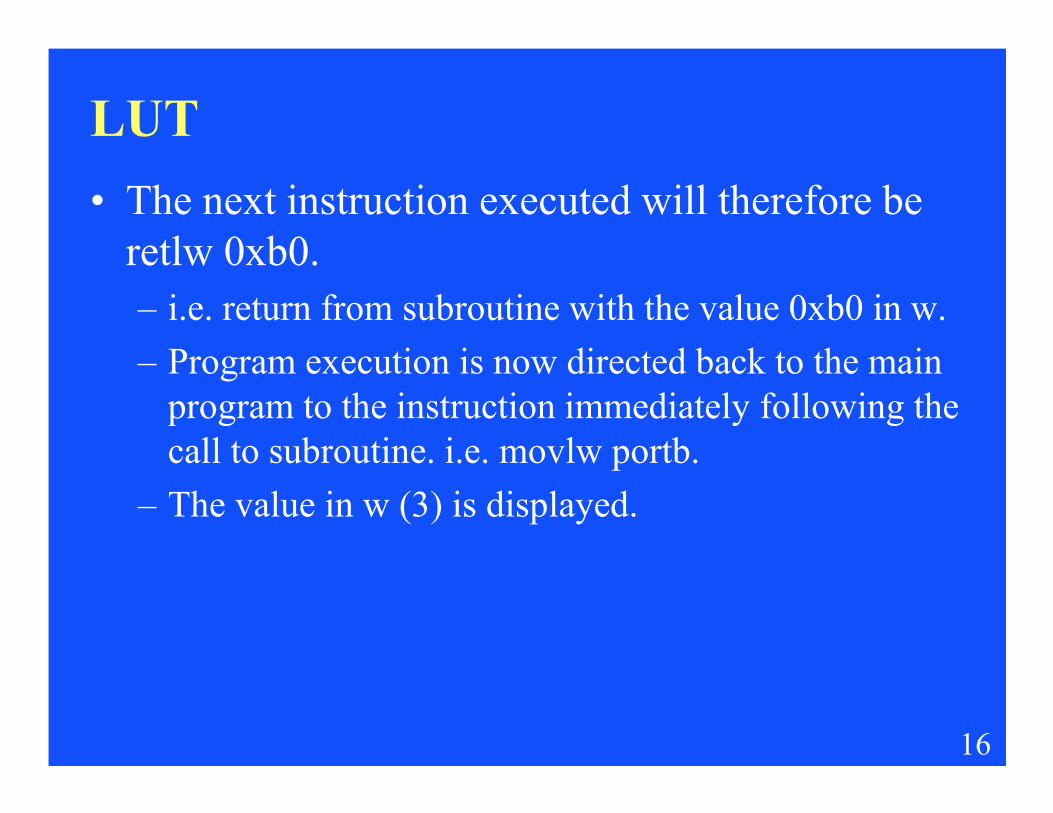
LUT
• The next instruction executed will therefore be
retlw 0xb0.
– i.e. return from subroutine with the value 0xb0 in w.
– Program execution is now directed back to the main
program to the instruction immediately following the
16
program to the instruction immediately following the
call to subroutine. i.e. movlw portb.
– The value in w (3) is displayed.

Exercise
• Write a program to find the value of y=2x2 using
a LUT. The possible values of x are 0, 1, 2, 3, 4
and 5.
17
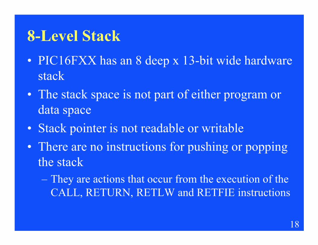
8-Level Stack
• PIC16FXX has an 8 deep x 13-bit wide hardware
stack
• The stack space is not part of either program or
data space
• Stack pointer is not readable or writable
18
• Stack pointer is not readable or writable
• There are no instructions for pushing or popping
the stack
– They are actions that occur from the execution of the
CALL, RETURN, RETLW and RETFIE instructions

8-Level Stack
• The entire 13-bit PC is “pushed” onto the stack
when a CALL instruction is executed or an
interrupt is acknowledged.
• The stack is “popped” in the event of a
RETURN, RETLW or a RETFIE instruction
19
RETURN, RETLW or a RETFIE instruction
execution
• The stack operates as a circular buffer.
– After the stack has been pushed eight times, the ninth
push overwrites the value that was stored from the
first push
20
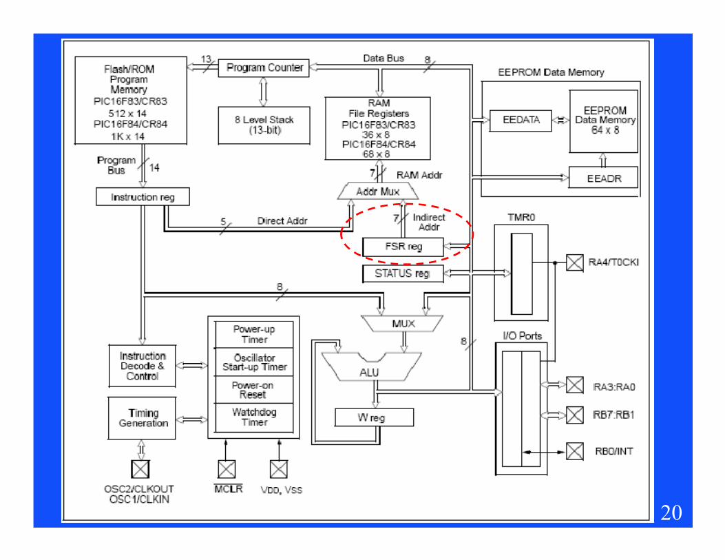
Indirect Addressing
• Allow you to look down a set of files and either
read them or write to them, with the least number
of instructions
• Two files are used for the indirect addressing function.
– File 00h (INDF - INDIRECT File)
21
– File 00h (INDF - INDIRECT File)
– File 004h (FSR - File Select Register)
• INDF register is not a physical register.
• Addressing INDF actually addresses the register
whose address is contained in the FSR register
(FSR is a pointer)
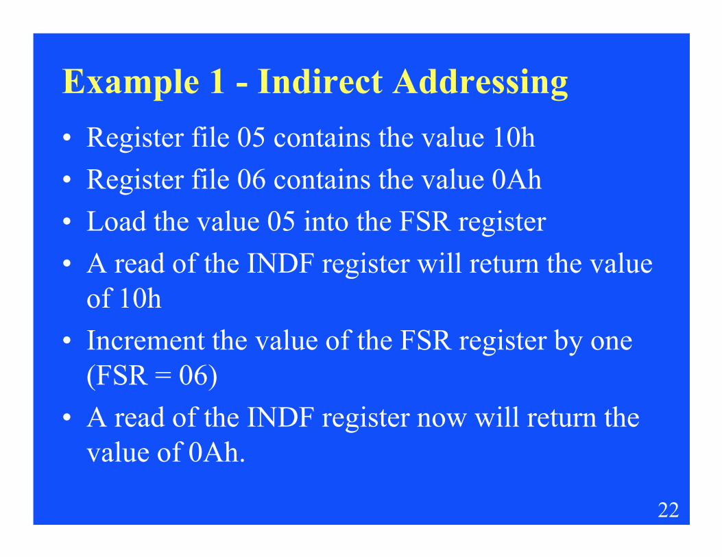
Example 1 - Indirect Addressing
• Register file 05 contains the value 10h
• Register file 06 contains the value 0Ah
• Load the value 05 into the FSR register
• A read of the INDF register will return the value
22
of 10h
• Increment the value of the FSR register by one
(FSR = 06)
• A read of the INDF register now will return the
value of 0Ah.
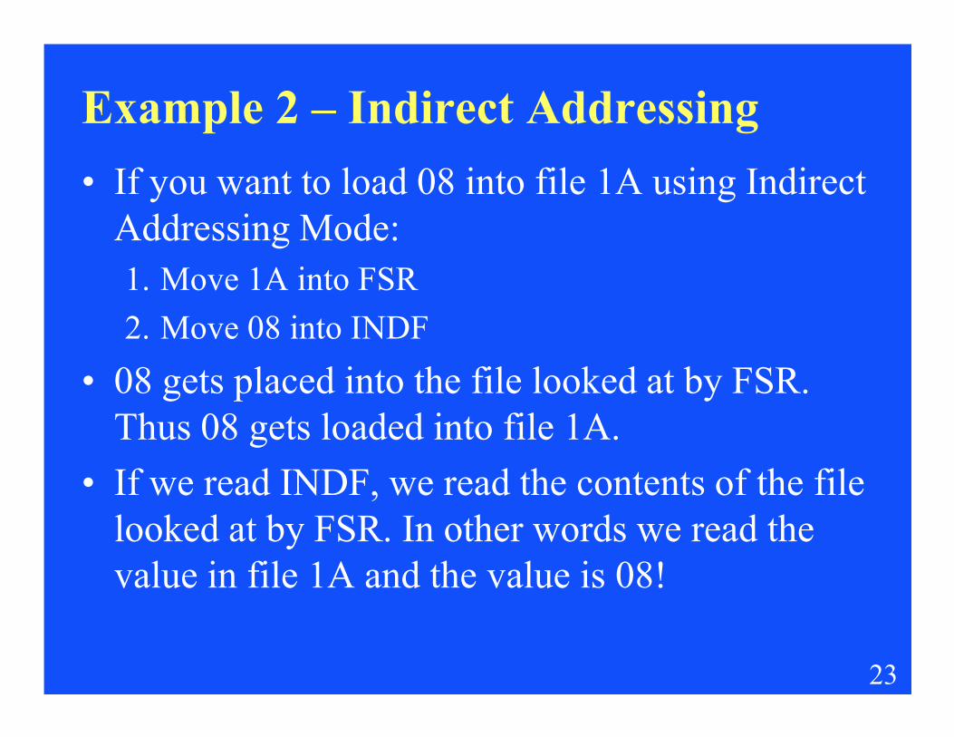
Example 2 – Indirect Addressing
• If you want to load 08 into file 1A using Indirect
Addressing Mode:
1. Move 1A into FSR
2. Move 08 into INDF
• 08 gets placed into the file looked at by FSR.
23
• 08 gets placed into the file looked at by FSR.
Thus 08 gets loaded into file 1A.
• If we read INDF, we read the contents of the file
looked at by FSR. In other words we read the
value in file 1A and the value is 08!
Exercise
• Write a program to clear RAM locations 20h-2Fh using indirect addressing
24
25
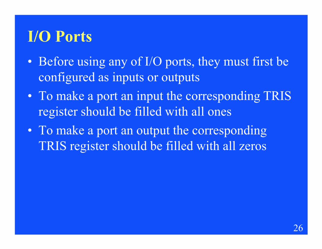
I/O Ports
• Before using any of I/O ports, they must first be
configured as inputs or outputs
• To make a port an input the corresponding TRIS
register should be filled with all ones
• To make a port an output the corresponding
26
• To make a port an output the corresponding
TRIS register should be filled with all zeros
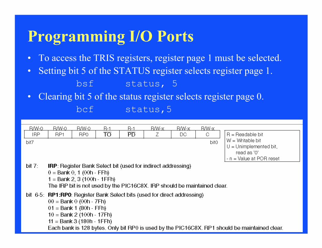
Programming I/O Ports
• To access the TRIS registers, register page 1 must be selected.
• Setting bit 5 of the STATUS register selects register page 1.
bsf status, 5
• Clearing bit 5 of the status register selects register page 0.
bcf status,5
27
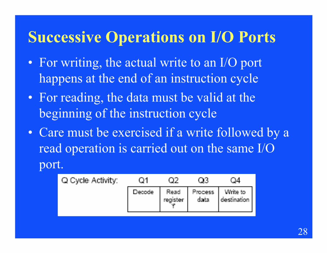
Successive Operations on I/O Ports
• For writing, the actual write to an I/O port
happens at the end of an instruction cycle
• For reading, the data must be valid at the
beginning of the instruction cycle
• Care must be exercised if a write followed by a
28
• Care must be exercised if a write followed by a
read operation is carried out on the same I/O
port.
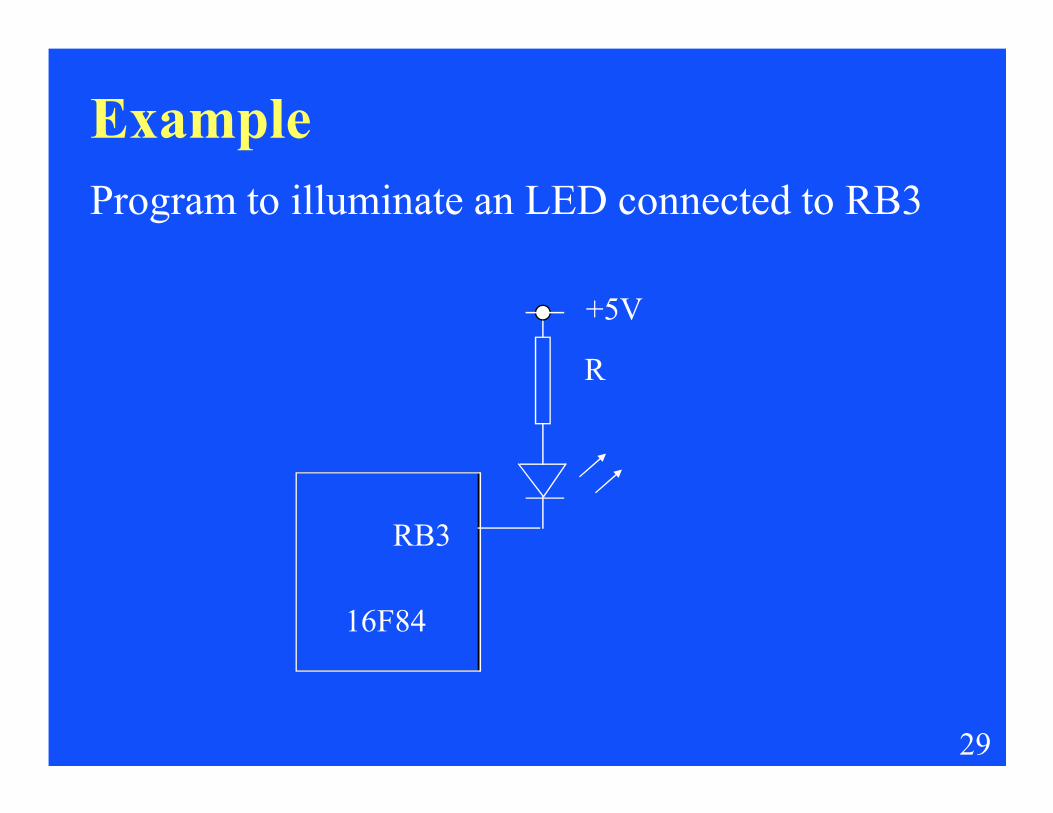
Example
Program to illuminate an LED connected to RB3
+5V
R
29
RB3
16F84
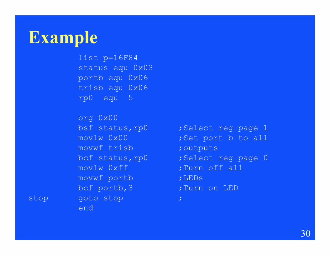
Examplelist p=16F84
status equ 0x03
portb equ 0x06
trisb equ 0x06
rp0 equ 5
org 0x00
bsf status,rp0 ;Select reg page 1
30
bsf status,rp0 ;Select reg page 1
movlw 0x00 ;Set port b to all
movwf trisb ;outputs
bcf status,rp0 ;Select reg page 0
movlw 0xff ;Turn off all
movwf portb ;LEDs
bcf portb,3 ;Turn on LED
stop goto stop ;
end
Exercise
• Write a program to make all the LEDs connected
to Port B blink three times and then stay on.
31
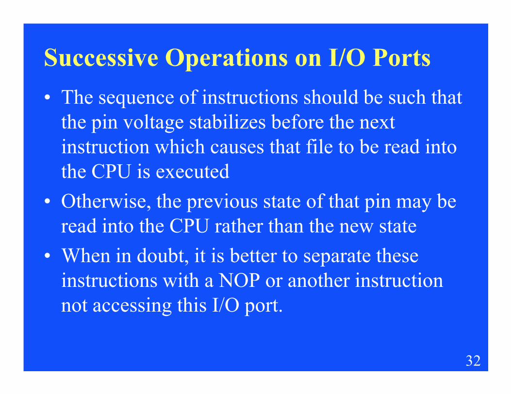
Successive Operations on I/O Ports
• The sequence of instructions should be such that
the pin voltage stabilizes before the next
instruction which causes that file to be read into
the CPU is executed
• Otherwise, the previous state of that pin may be
32
• Otherwise, the previous state of that pin may be
read into the CPU rather than the new state
• When in doubt, it is better to separate these
instructions with a NOP or another instruction
not accessing this I/O port.
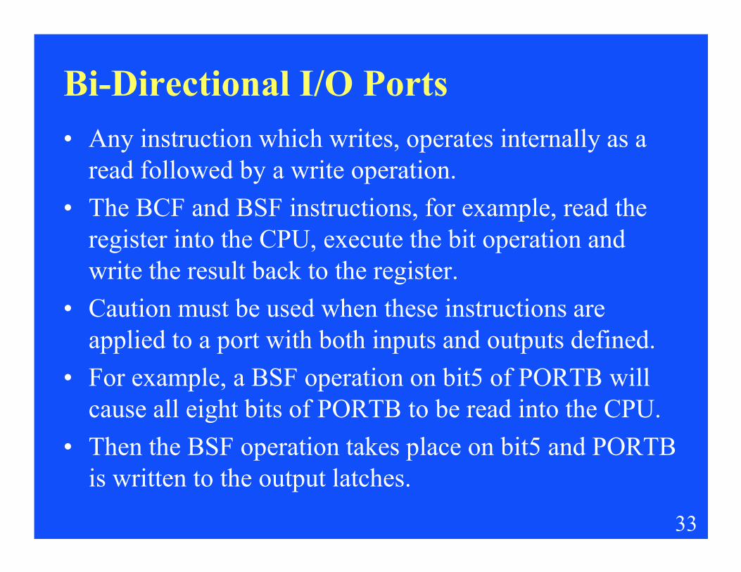
Bi-Directional I/O Ports
• Any instruction which writes, operates internally as a
read followed by a write operation.
• The BCF and BSF instructions, for example, read the
register into the CPU, execute the bit operation and
write the result back to the register.
33
• Caution must be used when these instructions are
applied to a port with both inputs and outputs defined.
• For example, a BSF operation on bit5 of PORTB will
cause all eight bits of PORTB to be read into the CPU.
• Then the BSF operation takes place on bit5 and PORTB
is written to the output latches.
Bi-Directional I/O Ports
• If another bit of PORTB is used as a bi-
directional I/O pin (i.e., bit0) and it is defined as
an input at this time, the input signal present on
the pin itself would be read into the CPU and
rewritten to the data latch of this particular pin,
34
rewritten to the data latch of this particular pin,
overwriting the previous content.
• As long as the pin stays in the input mode, no
problem occurs.
• However, if bit0 is switched into output mode
later on, the content of the data latch is unknown.