lecture 7 - step response & system behaviour
TRANSCRIPT

Lecture 7 Slide 1PYKC 2 Feb 2021 DE2 – Electronics 2
Lecture 7
Step Response & System Behaviour
Prof Peter YK Cheung
Dyson School of Design Engineering
URL: www.ee.ic.ac.uk/pcheung/teaching/DE2_EE/E-mail: [email protected]

Lecture 7 Slide 2PYKC 2 Feb 2021 DE2 – Electronics 2
Step Response of a 1st order system (DE1.3 L8 S3)
! Consider what happens to the circuit shown here as the switch is closed at t = 0. We are interested in y(t).
! Apply KVL around the loop, we get:
! This is a simple first-order differential equation with constant coefficients.
! We can model closing the switch at t=0 as:
! Then the solution of the differential equation is:
! You should be familiar with this from Electronics 1 last year: t = RC, the time-constant
y
𝑖 𝑡 𝑅 + 𝑦 𝑡 = 𝑥 𝑡 , 𝑏𝑢𝑡 𝑖 = 𝐶𝑑𝑦𝑑𝑡 𝑡ℎ𝑒𝑟𝑒𝑓𝑜𝑟𝑒
𝑅𝐶𝑑𝑦𝑑𝑡 + 𝑦 = 𝑥
𝑥 𝑡 = 𝑉 𝑢(𝑡)
y(t)
𝑦(𝑡) = 𝑉 1 − 𝑒 789: 𝑢(𝑡)
Lecture 7 Slide 3PYKC 2 Feb 2021 DE2 – Electronics 2
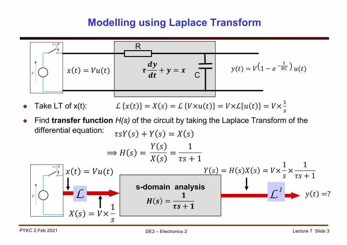
Modelling using Laplace Transform
𝝉𝒅𝒚𝒅𝒕 + 𝒚 = 𝒙
s-domain analysis
𝑯 𝒔 =𝟏
𝝉𝒔 + 𝟏L L-1
R
C
𝑥 𝑡 = 𝑉𝑢(𝑡)
𝑋 𝑠 = 𝑉×1𝑠
! Take LT of x(t): ℒ 𝑥 𝑡 = 𝑋 𝑠 = ℒ 𝑉×𝑢 𝑡 = 𝑉×ℒ 𝑢 𝑡 = 𝑉×GH
𝑥 𝑡 = 𝑉𝑢(𝑡) 𝑦(𝑡) = 𝑉 1 − 𝑒 789: 𝑢(𝑡)
! Find transfer function H(s) of the circuit by taking the Laplace Transform of the differential equation:
𝑌 𝑠 = 𝐻 𝑠 𝑋 𝑠 = 𝑉×1𝑠×
1𝜏𝑠 + 1
𝑦 𝑡 =?
𝜏𝑠𝑌 𝑠 + 𝑌 𝑠 = 𝑋 𝑠
⟹ 𝐻 𝑠 =𝑌 𝑠𝑋 𝑠 =
1𝜏𝑠 + 1

Lecture 7 Slide 4PYKC 2 Feb 2021 DE2 – Electronics 2
Forward & Inverse Laplace Transform
! Remember: the definition of the Laplace Transform is:L
L [x(t)] = X (s) = x(t)e−st dt0
∞
∫
L4.1
L −1
L −1 [X (s)] = x(t) = 12π j
X (s)est ds, ω → ∞σ− jω
σ+ jϖ
∫
! The definition of the Inverse Laplace Transform is:

Lecture 7 Slide 5PYKC 2 Feb 2021 DE2 – Electronics 2
Laplace transform Pairs (1)
! Finding inverse Laplace transform requires integration in the complex plane – beyond scope of this course.
! So, use a Laplace transform table (analogous to the Fourier Transform table).
L4.1
**

Lecture 7 Slide 6PYKC 2 Feb 2021 DE2 – Electronics 2
Laplace transform Pairs (2)
L4.1
*
****
Lecture 7 Slide 7PYKC 2 Feb 2021 DE2 – Electronics 2
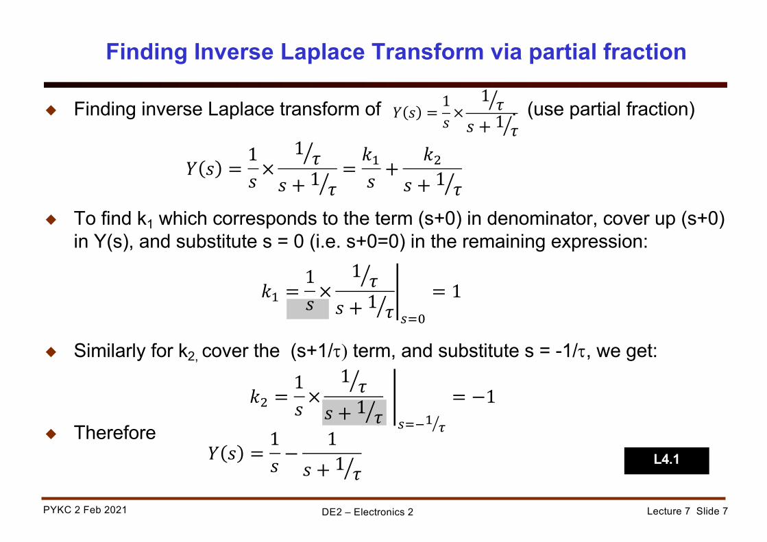
! Finding inverse Laplace transform of . (use partial fraction)
! To find k1 which corresponds to the term (s+0) in denominator, cover up (s+0) in Y(s), and substitute s = 0 (i.e. s+0=0) in the remaining expression:
! Similarly for k2, cover the (s+1/t) term, and substitute s = -1/t, we get:
! Therefore
Finding Inverse Laplace Transform via partial fraction
L4.1
𝑌 𝑠 =1𝑠 ×
N1 𝜏𝑠 + N1 𝜏
𝑌 𝑠 =1𝑠 ×
N1 𝜏𝑠 + N1 𝜏
=𝑘G𝑠 +
𝑘P𝑠 + N1 𝜏
𝑘P = Q1𝑠 ×
N1 𝜏𝑠 + N1 𝜏 HR7 NG S
= −1
𝑘G = Q1𝑠 ×
N1 𝜏𝑠 + N1 𝜏 HRT
= 1
𝑌 𝑠 =1𝑠 −
1𝑠 + N1 𝜏

Lecture 7 Slide 8PYKC 2 Feb 2021 DE2 – Electronics 2
! So, we get:
! Use Laplace Transform table, pair 5: 𝑒U8𝑢 𝑡 ⟺ GH7U
! Same as results from slide 2 using differential equation.
From Laplace Domain back to Time Domain
s-domain analysis
𝑯 𝒔 =N1 𝜏
𝑠 + N1 𝜏
L L-1𝑥 𝑡 = 𝑉𝑢(𝑡)
𝑋 𝑠 = 𝑉×1𝑠
𝑌 𝑠 = 𝐻 𝑠 𝑋 𝑠 = 𝑉×1𝑠 ×
N1 𝜏𝑠 + N1 𝜏
𝑦 𝑡 =?
𝑌 𝑠 = 𝑉(1𝑠−
1𝑠 + N1 𝜏
)
L
ℒ7G 𝑌 𝑠 = 𝑉ℒ7G1𝑠 −
1𝑠 + N1 𝜏
= 𝑉 𝑢 𝑡 − 𝑒78S 𝑢 𝑡 = 𝑉×(1 − 𝑒7
8S)×𝑢 𝑡

Lecture 7 Slide 9PYKC 2 Feb 2021 DE2 – Electronics 2
! Finding the inverse Laplace transform of .
! The partial fraction of this expression is less straight forward. If the power of numerator polynomial (M) is the same as that of denominator polynomial (N), we need to add the coefficient of the highest power in the numerator to the normal partial fraction form:
! Solve for k1 and k2 via “covering”:
! Therefore
! Using pairs 1 & 5:
Another Examples of Inverse Laplace Transform
22 5( 1)( 2)
ss s
-+ +
L4.1

Lecture 7 Slide 10PYKC 2 Feb 2021 DE2 – Electronics 2
! In Lab 3, we use the Bulb Board system, and it was known that the light bulb part of the system has a transfer function as shown:
! Therefore the light bulb itself has an exponential response with a time constant t = 38 ms.
! Remember, for a 1st order system, the output step response reaches the following percentages of final value after n x t, n=1,2,3,…:
Transfer function of a light bulb
Time = t 2t 3t 4t
Final value 63.2% 86.5% 95% 98.2%

Lecture 7 Slide 11PYKC 2 Feb 2021 DE2 – Electronics 2
! Once you know the transfer function B(s) of a system, you can evaluate its frequency response by evaluating H(s) at s = jw:
! Therefore, for our light bulb (not including the 2nd order electronic circuit, the frequency response is:
! From DE1 Electronics 1, you know that this is a low pass filter – gain drops with increasing frequency.
From Transfer function to Frequency Response
𝐵 𝑗𝜔 = Z𝐵(𝑠)HR[\
𝐵 𝑗𝜔 = ]1
(1 + 0.038𝑠) HR[\
𝐵(𝑗𝜔) = G(GbT.Tcd[\)
= GGbT.Tcde\e

Lecture 7 Slide 12PYKC 2 Feb 2021 DE2 – Electronics 2
! Let us consider a general second order system with a transfer function of the general form:
𝐻 𝑠 =𝑌(𝑠)𝑋(𝑠) =
𝑏P𝑠P + 𝑏G𝑠 + 𝑏T𝑠P + 𝑎G𝑠 + 𝑎T
! To simplify the problem a bit, let us assuming that b2 = b1 = 0. The above equation can be rewritten as:
! where: • 𝜔T = 𝑎T , the resonant (or natural) frequency in rad/sec
• 𝜁 = hiP hj
, the damping factor (no unit) (pronounced as zeta)
• 𝐾 = ljhj
, gain of the system
Transfer Function of a 2nd order system
𝐻 𝑠 =𝑏T
𝑠P + 𝑎G𝑠 + 𝑎T= 𝐾
𝜔TP
𝑠P + 2𝜁 𝜔T𝑠 + 𝜔TP

Lecture 7 Slide 13PYKC 2 Feb 2021 DE2 – Electronics 2
! Let us take the transfer function H(s) of the 2nd order system used in Bulb Box as an example:
• 𝜔T = 𝑎T = 31.62 , the resonant frequency = 5Hz
• 𝜁 = hiP hj
= oP GTTT
= 0.079 the damping factor (very small, ideal = 1)
• 𝐾 = ljhj= 1 , gain of the system at DC or zero frequency
! Since the damping factor is very small (much smaller than 1), this system is highly oscillatory.
Physical meaning of 𝝎𝟎, 𝝇, and 𝑲
𝐻 𝑠 =𝑏T
𝑠P + 𝑎G𝑠 + 𝑎T= 𝐾
𝜔TP
𝑠P + 2𝜁𝜔T𝑠 + 𝜔TP

Lecture 7 Slide 14PYKC 2 Feb 2021 DE2 – Electronics 2
! Let us consider the transfer function H(s) again:
! The unit step response of the system is (i.e. 𝑥 𝑡 = 𝑢 𝑡 , 𝑎𝑛𝑑 𝑋 𝑠 = 1/𝑠):
! We want to say something about the dynamic characteristic of this system by finding the natural frequency 𝜔T and the damping factor 𝜁.
! To do that, we find need to find the root of the quadratic: 𝑠P + 2𝜍𝜔T𝑠 + 𝜔TP
The importance of damping factor
𝐻 𝑠 =𝑏T
𝑠P + 𝑎G𝑠 + 𝑎T= 𝐾
𝜔TP
𝑠P + 2𝜁𝜔T𝑠 + 𝜔TP
𝑌 𝑠 =1𝑠𝐻 𝑠 =
1𝑠𝐾
𝜔TP
𝑠P + 2𝜁𝜔T𝑠 + 𝜔TP
𝑠 =−2𝜁𝜔T ± (2𝜁𝜔T)P −4𝜔TP
2= −𝜁𝜔T ± 𝜔T 𝜁P − 1

Lecture 7 Slide 15PYKC 2 Feb 2021 DE2 – Electronics 2
! Depending on the value of the damping factor 𝜁, there are five cases of interest, each having a specific behaviour:
! Root of denominator:
Five cases of behaviour
𝐻 𝑠 =𝑏T
𝑠P + 𝑎G𝑠 + 𝑎T= 𝐾
𝜔TP
𝑠P + 2𝜁𝜔T𝑠 + 𝜔TP
𝑠 = −𝜁𝜔T ± 𝜔T 𝜁P − 1

Lecture 7 Slide 16PYKC 2 Feb 2021 DE2 – Electronics 2
Step Response for different damping factors
underdamped
Overdamped
Critically damped
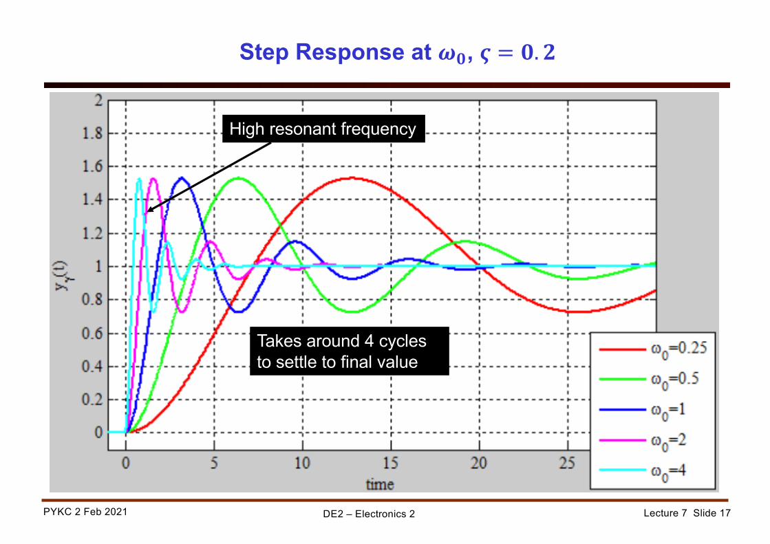
Lecture 7 Slide 17PYKC 2 Feb 2021 DE2 – Electronics 2
Step Response at 𝝎𝟎, 𝝇 = 𝟎. 𝟐
High resonant frequency
Takes around 4 cycles to settle to final value

Lecture 7 Slide 18PYKC 2 Feb 2021 DE2 – Electronics 2
Frequency response of 2nd order system
Normalised frequency ⁄𝜔 𝜔T
underdamped
Overdamped

Lecture 7 Slide 19PYKC 2 Feb 2021 DE2 – Electronics 2
A video demonstrating an underdamped oscillatory system

Lecture 7 Slide 20PYKC 2 Feb 2021 DE2 – Electronics 2
The Millennium Bridge