led/oled design using mixed-level simulation - … · these characteristics are then incorporated...
TRANSCRIPT

White Paper
April 2015
LED/OLED Design Using Mixed-Level Simulation
Authors
Mayank Bahl
Senior Staff
Scientist, Synopsys
Dan Herrmann
CAE Manager,
Synopsys
IntroductionOver the last two decades, there has been extensive research to improve the design of light-emitting diodes (LEDs) to enhance light extraction efficiency, improve beam shaping, and allow color tuning. Techniques such as patterned substrates, polarization-sensitive gratings, back reflectors, surface textures, and phosphor down-conversion have all been explored. Moreover, organic light-emitting diodes (OLEDs) have also garnered much attention in recent years due to their low cost, simple fabrication processes, thin film structure, and good spectral range. OLEDs can be fabricated on both rigid and flexible substrates, making them desirable for a wide range of applications such as color displays and solid state illumination.
Due to the range and scales of geometric structures used in LEDs and OLEDs, a variety of numerical techniques are required to efficiently and accurately analyze their performance and optimize their efficiency. In this paper, we present the use of a mixed-level simulation approach that unifies the use of electromagnetic (EM) wave-level and ray-level tools. This approach uses rigorous EM wave-based tools to completely characterize scattering from nanostructured surfaces and the far-field angular intensity distribution from the source region. These characteristics are then incorporated into a ray tracing simulator to obtain overall device performance. This approach uses a complete data transfer between the EM wave-level and the ray-level tools, allowing for rigorous comprehensive modeling, including polarization that is not possible through other means.
Problem: Typical Optical Aspects of LEDs/OLEDsComputational simulation has been an important tool for examining the underlying physics of LEDs and OLEDs, understanding the underlying physics of their operation, and providing design insights into increasing their performance. The choice of which simulation method to employ is usually governed by the optical aspects of the particular problem. LEDs and OLEDs are growing increasingly complex, and can include optical design aspects such as:
`` Geometric features varying in size over orders of magnitude:
– Thin films
– Micro/nano-patterned structures
– Thick planar layers, e.g., substrates
– Large structures associated with packaging
`` Periodically patterned structures for improved efficiency
`` Diffusers, surface and volumetric scatterers
`` Optimization of die placement
`` Source incoherence

LED/OLED Design Using Mixed-Level Simulation 2
Figure 1: Typical aspects of an OLED/LED design illustrated with (a) simplified OLED structure and (b) large structures associated with packaging.
No single optical simulation tool can address all of these aspects, as described in the following table.
Solution: Mixed-Level Simulation MethodologyA mixed-level simulation approach for LEDs and OLEDs must be used to unify the EM- and ray-based tools and circumvent their individual limitations. Additionally, this approach must allow for the complete data transfer between individual tools to ensure accuracy.
The individual simulation tools and corresponding numerical techniques used in this paper are listed below:
`` RSoft™ FullWAVE™: FDTD-based rigorous EM tool. Since FDTD is a direct solution of Maxwell’s curl equations, it can be used to model arbitrarily complex LED/OLED structures.
`` RSoft DiffractMOD™: RCWA-based rigorous EM tool widely used to efficiently simulate periodic structures.
`` RSoft LED Utility™: Based on FullWAVE and used to model the incoherent source aspect of LED/OLEDs.
`` LightTools®: Uses Monte Carlo Ray Tracing techniques and provides accurate predictions of output from systems that consist of sources, receivers and various optical elements.
`` Bidirectional Scattering Distribution Function (BSDF) Utility: Based on DiffractMOD and/or FullWAVE and used to characterize the scattering properties from the surface of an arbitrary structure.
`` RSoft BSDF User-Defined Optical Properties (UDOP) for LightTools: Uses the BSDF at a surface to represent an underlying structure that could not otherwise be simulated with geometric optics approximations, and includes polarization effects.
Our mixed-level approach can be summarized as follows:
`` Use a rigorous EM wave-based tool (FullWAVE and/or DiffractMOD) to characterize the sub-wavelength layered OLED structure as well as the micro-structures at the glass-air interface. The complete scattering information calculated by these tools is saved in an RSoft BSDF file.
`` Apply the calculated BSDF files as surface properties in the ray-based tool (LightTools) using the RSoft BSDF UDOP. The UDOP allows for complete data transfer, including the ability to include polarization effects and exact angular resolution.
Ray-Based Optical Simulation Tools EM-Based Optical Simulation Tools
Ray-optics-based techniques such as Monte Carlo ray tracing (RT) are based on geometrical optics. RT models the system as a collection of rays. The angle and intensity of transmission/reflection at interfaces is determined by Fresnel’s law.RT techniques are good for modeling photonic elements with large feature sizes and are commonly used to analyze:• Encapsulating structure design• Packaging• LED die placement• Back reflectors• Large size surface scatterers • Color tuning through phosphor modelingThe primary limitation of RT techniques is that they cannot model sub-wavelength geometric features where diffraction and interference effects are critical.
Techniques based on electromagnetic (EM) wave optics, such as Finite-Difference Time-Domain (FDTD) and Rigorous Coupled Wave Analysis (RCWA) solve Maxwell’s equations either directly or through some approximation.These techniques are good for modeling photonic elements with small feature sizes, including:• Sub-wavelength thin film stacks• Micro/nano structures for improved extraction efficiency• Photonic crystal/other periodic gratings • Random surface textures• Coupling to surface plasmon modes for back reflectorsThe primary limitation of these rigorous EM techniques is that they have difficulty analyzing larger structures due to computational limitations.
Packaging
Die placement
Cathode ETLHBLEMLEBLHTL
Organic
ITO
Glass
Sub-λ
mm’s
Scatteringparticles

LED/OLED Design Using Mixed-Level Simulation 3
`` Convert the far-field angular intensity distribution in glass calculated by the EM simulator (LED Utility) to a ray data source for use in LightTools.
`` Using the BSDF and ray data source, LightTools can then be used to model overall performance of the LED/OLED.
For detailed information about our mixed-level simulation approach, refer to Bahl et al. [1, 2].
Figure 2: Schematic of the combined EM (DiffractMOD +FullWAVE) and ray-tracing-based simulations. The simplified OLED structure is shown on the left, and the structure used in ray tracing is shown on the right.
Aside: Advantages of RSoft BSDF/UDOP Over Traditional BSDF TechniquesThere are several key advantages of the aforementioned approach compared to the traditional BSDF approaches used to link EM tools to ray tools. Some of the key advantages are listed and elaborated on below:
`` Synopsys’ mixed-level approach natively includes polarization effects. Traditional approaches lose polarization data through averaging, which is not accurate for polarization-sensitive structures. This is essential to accurately simulate polarized LEDs as shown later in Case Study 3.
Figure 3: How polarization is handled: a) Synopsys’ approach preserves polarization and includes cross-coupling, b) other approaches lose polarization data.
`` The exact angular resolution of diffraction orders is stored in the RSoft BSDF and is natively passed to the LightTools simulation through the RSoft BSDF UDOP (see Figure 4). Traditional approaches store data on an angular grid, which reduces accuracy (blue line in Figure 4); angles can ‘shift’ as well as ‘broaden’. This topic is explored further in Case Study 2 and depicted in Figure 11.
Glass
Emission layerTFS1) BSDF data forOLED structure via RCWA
2) FDTD simulationto get ray data inglass for source rays
3) BSDF for patternedGlass-Air interface via RCWA
4) Extraction efficiency viaray tracing
Pattern BSDF
Ray source
TFS BSDF
RSoft BSDF +LightTools UDOP Other approaches
‘s’ in
‘p’ in
‘s’ in
‘?’ out
‘p’ in
‘s’ out
?‘p’ out

LED/OLED Design Using Mixed-Level Simulation 4
Figure 4: How angular data for diffractive scattering is stored in BSDF files: a) Synopsys’ approach stores diffraction angles at discrete angles (red line), b) other approaches use an angular
grid (blue line), which reduces accuracy.
`` The RSoft BSDF UDOP uses a complete range of input angles: the ‘POI’ angle can vary from 0 to 360 degrees. Symmetry can be assumed if needed. Traditional approaches usually limit the ‘POI’ angle from 0 to 90 degrees and always assume symmetry.
Figure 5: Fully anisotropic angle dependence can be modeled with (a) RSoft UDOP unlike (b) traditional approaches
Case Study 1: Simple ‘Flat’ OLED StructureIn order to illustrate improved extraction efficiency due to surface patterning, first consider a simple a bottom-emitting green OLED based on a similar structure described in Adachi et.al. [3]. We will vary the relative position d of the Emission Layer (EML) from the cathode to find an optimum location that allows for maximum out-coupling. The structure and material information used for this example are shown in Figure 6.
Figure 6: Simplified OLED structure based on Adachi et al. [3] but with varying organic layer thickness. ‘d’ represents the cathode-EML separation.
The simulations were performed as follows:
`` All simulations were monochromatic and performed at a wavelength of 520 nm.
`` The EML was modeled in FullWAVE (FDTD) as an incoherent source, and the far field was converted to a source ray data file for use in LightTools. Note that the far field was measured within the glass layer, since the 1mm thick substrate is too large for any FDTD tool to handle.
`` The scattering due to the thin layer structure was calculated with DiffractMOD and saved as an RSoft BSDF file.
-60
0.4
0.3
0.2
0.1
0.0
-40 -20Angle (degree)
Tran
smitt
ed p
ower
20 40 600
180
270
90
0
POI
180
270
90
0
POI
0 90
AOI
0 90
AOI
Glass
Mg:Ag
Organic
ITO
EML125nm
d
Material name
Glass (substrate)
ITO (transparentelectrode)
Organic
Mg:Ag (cathode)
1.5
1.9 + i * 0.01
1.7
0.25 + i * 4.36
*Semi-infinite/1mm
160nm
125nm + ‘d’*
*Semi-infinite/250nm
Reflective index Thickness
LED/OLED Design Using Mixed-Level Simulation 5
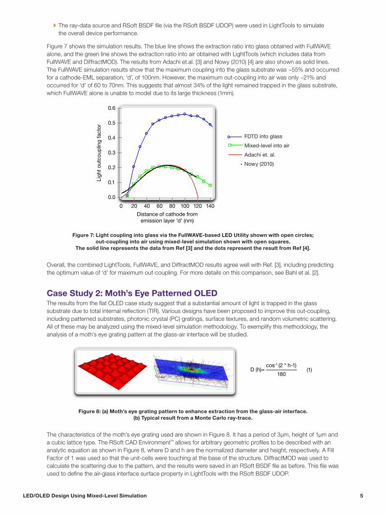
`` The ray-data source and RSoft BSDF file (via the RSoft BSDF UDOP) were used in LightTools to simulate the overall device performance.
Figure 7 shows the simulation results. The blue line shows the extraction ratio into glass obtained with FullWAVE alone, and the green line shows the extraction ratio into air obtained with LightTools (which includes data from FullWAVE and DiffractMOD). The results from Adachi et.al. [3] and Nowy (2010) [4] are also shown as solid lines. The FullWAVE simulation results show that the maximum coupling into the glass substrate was ~55% and occurred for a cathode-EML separation, ‘d’, of 100nm. However, the maximum out-coupling into air was only ~21% and occurred for ‘d’ of 60 to 70nm. This suggests that almost 34% of the light remained trapped in the glass substrate, which FullWAVE alone is unable to model due to its large thickness (1mm).
Figure 7: Light coupling into glass via the FullWAVE-based LED Utility shown with open circles; out-coupling into air using mixed-level simulation shown with open squares.
The solid line represents the data from Ref [3] and the dots represent the result from Ref [4].
Overall, the combined LightTools, FullWAVE, and DiffractMOD results agree well with Ref. [3], including predicting the optimum value of ‘d’ for maximum out-coupling. For more details on this comparison, see Bahl et al. [2].
Case Study 2: Moth’s Eye Patterned OLEDThe results from the flat OLED case study suggest that a substantial amount of light is trapped in the glass substrate due to total internal reflection (TIR). Various designs have been proposed to improve this out-coupling, including patterned substrates, photonic crystal (PC) gratings, surface textures, and random volumetric scattering. All of these may be analyzed using the mixed-level simulation methodology. To exemplify this methodology, the analysis of a moth’s eye grating pattern at the glass-air interface will be studied.
Figure 8: (a) Moth’s eye grating pattern to enhance extraction from the glass-air interface. (b) Typical result from a Monte Carlo ray-trace.
The characteristics of the moth’s eye grating used are shown in Figure 8. It has a period of 3μm, height of 1μm and a cubic lattice type. The RSoft CAD Environment™ allows for arbitrary geometric profiles to be described with an analytic equation as shown in Figure 8, where D and h are the normalized diameter and height, respectively. A Fill Factor of 1 was used so that the unit-cells were touching at the base of the structure. DiffractMOD was used to calculate the scattering due to the pattern, and the results were saved in an RSoft BSDF file as before. This file was used to define the air-glass interface surface property in LightTools with the RSoft BSDF UDOP.
0.6
0.0
0 20 40 60 80 100 140120
0.1
0.2
0.3
0.4
0.5
Ligh
t ou
tcou
plin
g fa
ctor
Distance of cathode fromemission layer ‘d’ (nm)
FDTD into glass
Mixed-level into air
Adachi et. al.
Nowy (2010)
D (h)=cos-1 (2 * h-1)
180(1)

LED/OLED Design Using Mixed-Level Simulation 6
Figure 9: Light out-coupling into air using mixed-level simulation with (red line) and without (green line) the moth’s eye grating.
Figure 9 shows the out-coupling results with (red line) and without (green line) the moth’s eye grating pattern applied at the glass-air interface. The optimum out-coupling for the flat structure was 21% as previously indicated, whereas the patterned structure increased to 30%, which is a 43% out-coupling efficiency enhancement.
The far-field intensity distribution calculated in air by LightTools (both with and without the moth’s eye grating) is shown in Figure 10. The peak field intensity is significantly higher with the presence of the moth’s eye grating. In addition, the presence of the grating also improves the angular uniformity of the far-field intensity distribution as shown in Figure 10c. Additional enhancements may be achievable through further optimization of the moth’s eye grating.
Figure 10: Calculated angular far-field intensity for (a) the Flat interface structure versus (b) the moth’s eye grating. (c) Cross-cut at horizontal angle (H=0), showing enhanced out-coupling and improved angular uniformity.
An example demonstrating the impact of the angular resolution in the BSDF file, and the importance of using RSoft BSDF UDOP instead, is shown in Figure 11. It consists of a glass-air interface patterned with a moth’s eye grating pattern. The launch consists of a source with a large angular spread and the field pattern is measured by a receiver a certain distance away from the interface.
With grating
Without grating
0.0
0 20 40 60 80 100 140120
0.1
0.2
0.3
Ligh
t ou
tcou
plin
g fa
ctor
Distance of cathode fromemission layer ‘d’ (nm)
With grating
Without grating
0.0
0
0.16
0.137
0.114
0.0914
0.0457
0.0229
-80 -40-60 -20 0 20 40 8060
0.03
0.15
0.12
0.09
0.06
0.18
Vertical angle (degrees)
Cross-cut of farfield intensity distribution at H=0

LED/OLED Design Using Mixed-Level Simulation 7
Figure 11: a) Moth’s eye patterned glass-air interface. Launch consists of a source with large angular spread, and b) the far-field pattern at a receiver for the UDOP
(blue line) versus the BSDF for various output angular resolutions.
Figure 11 shows that the results using traditional measured BSDF vary dramatically based on the output angular resolution and requires very fine output angular resolution to get results similar to the RSoft UDOP (which is independent of the output resolution). The requirements of a finer BSDF output resolution not only requires more memory, but could also lead to inefficiencies when reading large size files.
Case Study 3: Polarized LEDRecent research demonstrates numerous applications of polarized LEDs, including high-efficiency backlit LCDs, projection display lighting, improved contrast in general illumination (due to reduced glare), sensing, and communication. As shown above, traditional approaches lose polarization data through averaging, which is not accurate for polarization-sensitive structures. The RSoft BSDF UDOP can natively include polarization effects, which are essential to accurately simulate polarized LEDs; for more details, see Bahl et al. [1].
One example of a polarized LED structure is shown in Figure 12 based on M. Ma et al. [5]. It uses a wire-grid polarizer (WGP) at the substrate-air interface for a back-emitting GaInN/GaN LED. WGPs are sub-wavelength metallic gratings that can be used to filter light based on polarization. The light reflected from WGP (primarily the non-transmitted polarization) can be reused through a polarization conversion and recycling mechanism.
Figure 12: a) Back-emitting GaInN/GaN LED with Al-based wire grid polarizer on the substrate-air interface. b) The power emitted from the LED using the two approaches: RSoft UDOP (blue line) and
traditional BSDF (green line) as a function of the orientation angle of a rotating linear polarizer.
UDOPBSDF res=1 degBSDF res=5 degBSDF res=10 deg
Glasssubstance
Launch (largeangular spread)
Motheye grating
YX
Z
Receiver
Using UDOP
Using BSDF
0.0
-80 -40-60 -20 0 20 40 8060
0.1
0.50.60.70.80.9
0.40.30.2
1.0
Rotating linear polarizer angle (degrees)
GaN LED with wire-grid polarizerReceiver
Polarizing element
LED semiconductor
Sapphire substrate
AI WGP
TE mode lightTM mode light

04/15.AP.CS5715.
Synopsys, Inc. • 690 East Middlefield Road • Mountain View, CA 94043 • www.synopsys.com
©2015 Synopsys, Inc. All rights reserved. Synopsys is a trademark of Synopsys, Inc. in the United States and other countries. A list of Synopsys trademarks is available at http://www.synopsys.com/copyright.html . All other names mentioned herein are trademarks or registered trademarks of their respective owners.
The parameters of the structure are a wavelength of 0.46 μm, a period of 0.15 μm, a duty cycle of 0.26, a depth of 0.19 μm, and the grating and substrate are aluminum and sapphire, respectively. This structure was simulated with DiffractMOD, although FullWAVE could also have been used. The generated BSDF, which contains polarization data, was then used in LightTools in two different ways:
`` Directly through the RSoft BSDF UDOP
`` To mimic other approaches, the RSoft BSDF file was converted to a LightTools BSDF and applied as a measured BSDF surface property in LightTools.
The polarization of the emitted light was measured by placing a rotating linear polarizer between the LED and the detector. The results from the two approaches are shown in Figure 12b. It is clear from these results that the Synopsys approach includes polarization and shows the theoretically expected cosine-squared dependence (and is also closer to the experimental results in the reference). In contrast, the other approaches show completely unpolarized emission. These other approaches are therefore not suitable for LEDs when polarization effects are important.
SummaryModern optical and photonic designs that contain geometric features that vary in size over orders of magnitude require a variety of numerical techniques to optimize their design and analyze their performance. A mixed-level simulation methodology that combines several techniques (FullWAVE, DiffractMOD, and LightTools) has been presented. FullWAVE used with the LED Utility was used to create an incoherent source for ray tracing, while DiffractMOD was used to generate the BSDF for both the thin stack OLED and the moth’s eye grating at the glass-air interface. This information was then incorporated into a LightTools simulation through ray data source and surface property interfaces, which permitted the full analysis of the device performance. Three case studies demonstrated that the use of the RSoft BSDF UDOP allows for a complete data transfer between the EM wave-based tools and ray-based tool, and allows for design and optimization of LED and OLED structures. Moreover, the advantages of the RSoft BSDF UDOP over the traditional BSDF approach were also demonstrated, including modeling of polarized LEDs.
References[1] Mayank Bahl; Gui-Rong Zhou; Evan Heller; William Cassarly; Mingming Jiang, et al. “Mixed-level optical
simulations of light-emitting diodes based on a combination of rigorous electromagnetic solvers and Monte Carlo ray-tracing methods”, Opt. Eng. 54(4), 045105 (Apr 21, 2015). ; http://dx.doi.org/10.1117/1.OE.54.4.045105.
[2] Bahl, M., Zhou, G., Heller, E., Cassarly, W., Jiang, M., Scarmozzino, R., and Gregory, G.G, “Optical Simulations of Organic Light-Emitting Diodes through a Combination of Rigorous Electromagnetic Solvers and Monte Carlo Ray-Tracing Methods”, Proc. SPIE, 9190 (2014).
[3] Adachi,C., Baldo, M.A., Thompson, M.E, and Forrest, S.R., “Nearly 100% internal phosphorescence efficiency in an organic light emitting device,” J. Appl. Phys. 90, 5048 (2001).
[4] Nowy, S.,“Understanding losses in OLEDs: optical device simulation and electrical characterization using impedance spectroscopy”, Dissertation, 73 (2010).
[5] Ma, M., Meyaard, D., Shan, Q., Cho, J., Schubert, E., Kim, G., and Sone, C., “Polarized light emission from GaInN light-emitting diodes embedded with subwavelength aluminum wire-grid polarizers,” Applied Physics Letters 101, (2012).