lg display · pdf filesupplier lg.philips lcd co., ltd. please return 1 copy for your...
TRANSCRIPT
DATA DISPLAY GROUP
Datasheet LG Display LB064V02-TD01
HD-15-259
The information contained in this document has been carefully researched and is, to the best of our knowledge, accurate. However, we assume no liability for any product failures or damages, immediate or consequential, resulting from the use of the information provided herein. Our products are not intended for use in systems in which failures of product could result in personal injury. All trademarks mentioned herein are property of their respective owners. All specifications are subject to change without notice.

Product Specification
1 / 24
LB064V02Liquid Crystal Display
Ver. 1.0 Oct. 13, 2005
SPECIFICATIONFOR
APPROVAL
6.4” V (640 X RGB X 480 ) TFT – LCDTitle
MODEL
BUYER
LB064V02MODEL
TD01SUFFIX
LG.Philips LCD Co., Ltd.SUPPLIER
Please return 1 copy for your confirmation withyour signature and comments.
/
/
/
DATESIGNATURE
))
((
Final Specification●
Preliminary Specification
C. S. KYEONG /G. Manager
Product Engineering Dept.LG. Philips LCD Co., Ltd
APPROVED BY DATE
REVIEWED BY
PREPARED BY
S. D. Jung /Manager
H. Y. Park /Project Leader Oct.13.2005
Oct.13.2005
Oct.13.2005
Product Specification
2 / 24
LB064V02Liquid Crystal Display
Ver. 1.0 Oct. 13, 2005
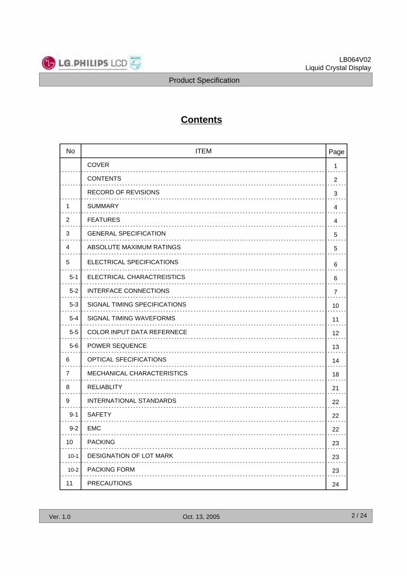
Contents
4SUMMARY1
4FEATURES2
24PRECAUTIONS11
12
7INTERFACE CONNECTIONS5-2
COLOR INPUT DATA REFERNECE5-5
23DESIGNATION OF LOT MARK10-1
23PACKING FORM10-2
23PACKING10
22EMC9-2
1COVER
2CONTENTS
3RECORD OF REVISIONS
5GENERAL SPECIFICATION3
5ABSOLUTE MAXIMUM RATINGS4
6ELECTRICAL SPECIFICATIONS5
6ELECTRICAL CHARACTREISTICS5-1
10SIGNAL TIMING SPECIFICATIONS5-3
11SIGNAL TIMING WAVEFORMS5-4
13POWER SEQUENCE5-6
14OPTICAL SFECIFICATIONS6
18MECHANICAL CHARACTERISTICS7
21RELIABLITY8
22INTERNATIONAL STANDARDS9
22SAFETY9-1
PageITEMNo
Product Specification
3 / 24
LB064V02Liquid Crystal Display
Ver. 1.0 Oct. 13, 2005
RECORD OF REVISIONS
Note
Final Version-Oct.13.20051.0
First Draft (Preliminary)-Aug. 30. 20050.0
DescriptionPageRevision DateRevision No
Product Specification
4 / 24
LB064V02Liquid Crystal Display
Ver. 1.0 Oct. 13, 2005
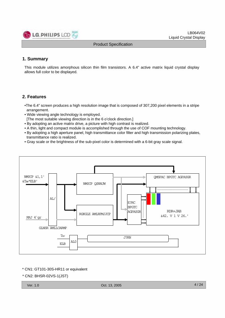
1. Summary
This module utilizes amorphous silicon thin film transistors. A 6.4” active matrix liquid crystal display allows full color to be displayed.
2. Features
•The 6.4” screen produces a high resolution image that is composed of 307,200 pixel elements in a stripearrangement.
• Wide viewing angle technology is employed. [The most suitable viewing direction is in the 6 o’clock direction.]
• By adopting an active matrix drive, a picture with high contrast is realized.• A thin, light and compact module is accomplished through the use of COF mounting technology.• By adopting a high aperture panel, high transmittance color filter and high transmission polarizing plates, transmittance ratio is realized.
• Gray scale or the brightness of the sub-pixel color is determined with a 6-bit gray scale signal.
INPUT CONNECTOR
POWER SUPPLY
TIMING CONTROLLER
SOURCE DRIVE CIRCUIT
TFT-LCD(640 X 3 X 480)
GATEDRIVECIRCUIT
POWER (3.3)(VDD,GND)
LAMPVBL
GNDCN2
CN1
TTL 6bit
* CN1: GT101-30S-HR11 or equivalent
* CN2: BHSR-02VS-1(JST)
Product Specification
5 / 24
LB064V02Liquid Crystal Display
Ver. 1.0 Oct. 13, 2005
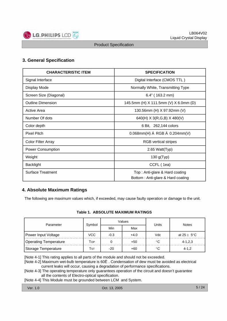
3. General Specification
2.65 Watt(Typ)Power Consumption
640(H) X 3(R,G,B) X 480(V)Number Of dots
Digital Interface (CMOS TTL )Signal Interface
6.4” ( 163.2 mm)Screen Size (Diagonal)
0.068mm(H) × RGB × 0.204mm(V)Pixel Pitch
Top : Anti-glare & Hard coating Bottom : Anti-glare & Hard coating
Surface Treatment
CCFL ( 1ea)Backlight
130 g(Typ)Weight
RGB vertical stripesColor Filter Array
6 Bit, 262,144 colorsColor depth
130.56mm (H) X 97.92mm (V)Active Area
145.5mm (H) X 111.5mm (V) X 6.0mm (D)Outline Dimension
Normally White, Transmitting TypeDisplay Mode
SPECIFICATIONCHARACTERISTIC ITEM
4. Absolute Maximum Ratings
The following are maximum values which, if exceeded, may cause faulty operation or damage to the unit.
Table 1. ABSOLUTE MAXIMUM RATINGS
Units
4-1,2°C+60-20TSTStorage Temperature
4-1,2,3°C+500TOPOperating Temperature
at 25 ± 5°CVdc+4.0-0.3VCCPower Input Voltage
MaxMinParameter Notes
ValuesSymbol
[Note 4-1] This rating applies to all parts of the module and should not be exceeded.[Note 4-2] Maximum wet-bulb temperature is 60℃. Condensation of dew must be avoided as electrical
current leaks will occur, causing a degradation of performance specifications.[Note 4-3] The operating temperature only guarantees operation of the circuit and doesn’t guarantee
all the contents of Electro-optical specification.[Note 4-4] This Module must be grounded between LCM and System.

Product Specification
6 / 24
LB064V02Liquid Crystal Display
Ver. 1.0 Oct. 13, 2005
5. Electrical Specifications
5-1. Electrical Characteristics
The LB064V02 requires two power inputs. One is employed to power the LCD electronics and to drive the TFT array and liquid crystal. The second input which powers the CCFL, is typically generated by an inverter. The inverter is an external unit to the LCD.
Table 2. ELECTRICAL CHARACTERISTICS
Kick-Off Voltage (*4)
*2kHz806040fBLOperating Frequency
at IBL=TYPWatt2.252.04-PBLPower Consumption
Ta=-30℃VRMS1200--Ta=25℃VRMS1000--
Vs
±10[%]VRMS370340325VBLOperating Voltage
mARMS6.56.03.0IBLOperating Current
LAMP :
*1Watt0.750.53-PcPower Consumption
Vdc3.63.33.0VCCPower Supply Input Voltage
*1mA210160-ICCPower Supply Input Current
*6Hrs--20,000Life Time
MODULE :
Parameter SymbolMaxTypMin
NotesUnitValues
Note)The design of the inverter must have specifications for the lamp in LCD Assembly. The performanceof the Lamp in LCM, for example life time or brightness, is extremely influenced by the characteristics of the DC-AC inverter. So all the parameters of an inverter should be carefully designed so as not to produce too much leakage current from high-voltage output of the inverter. When you design or order the inverter, please make sure unwanted lighting caused by the mismatch of the lamp and the inverter(no lighting, flicker, etc) never occurs. When you confirm it, the LCD Assembly should be operated in the same condition as installedin your instrument.
* 1. VCC=3.3V, 25°C, fV (frame frequency) = 60Hz condition, whereas mosaic pattern(Typ),full blackpattern(Max) is displayed. [LDO output voltage(3.3V) is applied.]
* 2. This frequency range means the range to keep within ±10% change of electrical and optical characteristics.
* 3. This frequency range means not affecting to lamp life and reliability characteristics.(The lamp frequency should be selected as different as possible from display horizontalsynchronous signal (Including harmonic frequency of this scanning frequency) to avoid “Beat”interference which may be observed on the screen as horizontal stripes like moving wave.

Product Specification
7 / 24
LB064V02Liquid Crystal Display
Ver. 1.0 Oct. 13, 2005
.
5-2. Interface ConnectionsThis LCD employs Two interface connections, a 30 pin connector is used for the module electronics interface and the other connectors is used for the integral backlight system.The electronics interface connector is a model GT101-30S-HR11 manufactured by LS Cable
* Asymmetry rate:
( I p – I –p |) / Irms * 100%
•Distortion rate:I p (or I –p) / Irms
Requirements for a system inverter design, which is intended to have a better display performance, a better power efficiency and a more reliable lamp, are as follows. It shall help increase the lamp lifetimeand reduce leakage current. Inverter should be designed to be subject to the conditions belowA. The asymmetry rate of the inverter waveform should be less than 10%.B. The distortion rate of the waveform should be within √2 ± 10%.
* Inverter output waveform had better be more similar to ideal sine wave.
C. There should not be any spikes in the waveform.D. Lamp current should not exceed the “MAX” value under the “Operating Temperature” (it is
prohibited to exceed the “MAX.” value even if it is operated in the guaranteed temperature). When lamp current exceed the maximum value for a long time, it may cause a smoking andIgnition.Therefore, it is recommended that the inverter have the current limited circuit that is used as aprotection circuit and/or the lamp current-controlled inverter.
∗ Do not attaches a conducting tape to lamp connecting wire.If the lamp wire attach to a conducting tape, TFT-LCD Module has a low luminance and the inverterhas abnormal action. Because leakage current is occurred between lamp wire and conducting tape.
I p
I -p
.
This phenomenon is caused by interference between lamp (CCFL) lighting frequency andLCD horizontal synchronous signal.)
* 4. The “MAX” of “Kick-Off Voltage” means the minimum voltage for inverter to turn on the CCFLnormally in the LCD module. However this isn’t the values that we can assure stability ofstarting lamp on condition that the module is installed in your set.It should be careful that “Kick-Off Voltage” is changed by an increase of stray capacitance in your set, inverter method, value of ballast capacitor in your inverter and so on.Especially, the value of “Kick-Off Voltage” is higher in low temperature condition than innormal temperature condition, because impedance of CCFL is increased.The voltage above VS should be applied to the lamps for more than 1 second for start-up. Otherwise, the lamps may not be turned on. The used lamp current is the lamp typical current.
* 5. The time needed to achieve not less than 95%brightness of the center part of lamp. The brightness of the lamp after being lighted for 5 minutes is defined as 100%.
* 6. “Life time” is defined as the time that the lamp brightness decreases to 50% from original brightness at IBL=TYP; continuous lighting, Ta=25℃.
Product Specification
8 / 24
LB064V02Liquid Crystal Display
Ver. 1.0 Oct. 13, 2005
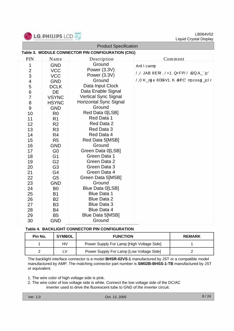
Table 3. MODULE CONNECTOR PIN CONFIGURATION (CN1)PIN Name Description Comment
123456789101112131415161718192021222324252627282930
GNDVCCVCCGNDDCLK
DEVSYNCHSYNC
GNDR0R1R2R3R4R5
GNDG0G1G2G3G4G5
GNDB0B1B2B3B4B5
GND
GroundPower (3.3V)Power (3.3V)
GroundData Input Clock
Data Enable SignalVertical Sync Signal
Horizontal Sync SignalGround
Red Data 0[LSB]Red Data 1Red Data 2 Red Data 3Red Data 4
Red Data 5[MSB]Ground
Green Data 0[LSB]Green Data 1Green Data 2Green Data 3Green Data 4
Green Data 5[MSB]Ground
Blue Data 0[LSB]Blue Data 1Blue Data 2Blue Data 3Blue Data 4
Blue Data 5[MSB]Ground
Connector
1.1 LCD : GT101-30S-HR11 (LS Cable)
1.2 Mating : FI-X30M (JAE) or equivalent
The backlight interface connector is a model BHSR-02VS-1 manufactured by JST or a compatible model manufactured by AMP. The matching connector part number is SM02B-BHSS-1-TB manufactured by JSTor equivalent.
1. The wire color of high voltage side is pink.2. The wire color of low voltage side is white. Connect the low voltage side of the DC/AC
inverter used to drive the fluorescent tube to GND of the inverter circuit.
2Power Supply For Lamp [Low Voltage Side]LV2
1
REMARK
Power Supply For Lamp [High Voltage Side]HV1
FUNCTIONSYMBOLPin No.
Table 4. BACKLIGHT CONNECTOR PIN CONFIGURATION

Product Specification
9 / 24
LB064V02Liquid Crystal Display
Ver. 1.0 Oct. 13, 2005
5-3. Signal Timing SpecificationsTable 4. TIMING TABLE
480480480tWVAWidth-Active
640640640tWHAWidth-Active
tCLK564016tHBPHorizontal back
porch
402416tHFPHorizontal front porch
tHP40332tVBPVertical back porch
15102tVFPVertical front porch
tHP
540525486Tvp Period
422tWVWidth
1309624tWHWidth tCLK
880800720ThpPeriodHsync
Vsync
DataEnable
MHz282522fCLK FrequencyDCLK
NoteUnitMaxTypMinSymbolITEM
DCLK,Data Enable, Hsync, Vsync Condition : VCC =3.3V
Low: 0.3VCC
High: 0.7VCC
Hsync
Date Enable
Vsync
Date Enable
tWH
tHP
tHFPtHBP
tVP
tWV
tVBPtVFP
tWHA
tWVA
5-4. Signal Timing Waveforms
Product Specification
10 / 24
LB064V02Liquid Crystal Display
Ver. 1.0 Oct. 13, 2005
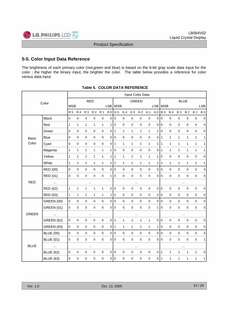
5-5. Color Input Data Reference
The brightness of each primary color (red,green and blue) is based on the 6-bit gray scale data input for thecolor ; the higher the binary input, the brighter the color. The table below provides a reference for color versus data input.
Table 5. COLOR DATA REFERENCE
0 0 0 0 0 00 0 0 0 0 00 0 0 0 0 0GREEN (00)
GREEN
0 0 0 0 0 00 0 0 0 0 10 0 0 0 0 0GREEN (01)
………...
0 0 0 0 0 01 1 1 1 1 00 0 0 0 0 0GREEN (62)
0 0 0 0 0 01 1 1 1 1 10 0 0 0 0 0GREEN (63)
0 0 0 0 0 00 0 0 0 0 00 0 0 0 0 0RED (00)
RED
0 0 0 0 0 00 0 0 0 0 00 0 0 0 0 1RED (01)
…………
0 0 0 0 0 00 0 0 0 0 01 1 1 1 1 0RED (62)
0 0 0 0 0 00 0 0 0 0 01 1 1 1 1 1RED (63)
0 0 0 0 0 10 0 0 0 0 00 0 0 0 0 0BLUE (01)
…………
1 1 1 1 1 00 0 0 0 0 00 0 0 0 0 0BLUE (62)
1 1 1 1 1 10 0 0 0 0 00 0 0 0 0 0BLUE (63)
BLUE (00)
White
Yellow
Magenta
Cyan
Blue
Green
Red
Black 0 0 0 0 0 00 0 0 0 0 00 0 0 0 0 0
BasicColor
0 0 0 0 0 00 0 0 0 0 01 1 1 1 1 1
0 0 0 0 0 01 1 1 1 1 10 0 0 0 0 0
1 1 1 1 1 10 0 0 0 0 00 0 0 0 0 0
1 1 1 1 1 11 1 1 1 1 10 0 0 0 0 0
1 1 1 1 1 10 0 0 0 0 01 1 1 1 1 1
0 0 0 0 0 01 1 1 1 1 11 1 1 1 1 1
1 1 1 1 1 11 1 1 1 1 11 1 1 1 1 1
BLUEMSB LSB
GREENMSB LSB
REDMSB LSB
B 5 B 4 B 3 B 2 B 1 B 0G 5 G 4 G 3 G 2 G 1 G 0R 5 R 4 R 3 R 2 R 1 R 0
0 0 0 0 0 00 0 0 0 0 00 0 0 0 0 0
BLUE
Color
Input Color Data
Product Specification
11 / 24
LB064V02Liquid Crystal Display
Ver. 1.0 Oct. 13, 2005
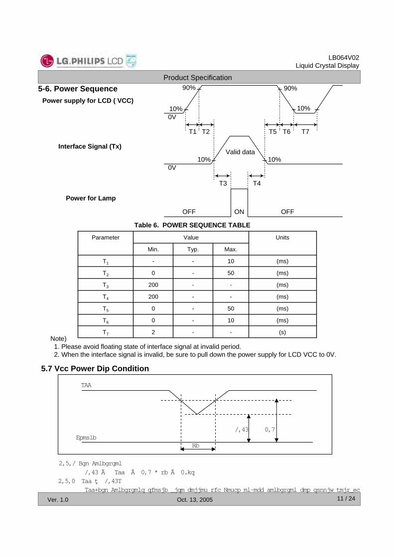
5-6. Power Sequence
Note)1. Please avoid floating state of interface signal at invalid period.2. When the interface signal is invalid, be sure to pull down the power supply for LCD VCC to 0V.
(s)--2T7
(ms)10-0T6
(ms)50-0T5
(ms)--200T4
(ms)--200T3
(ms)50-0T2
(ms)10--T1
Max.Typ.Min.
UnitsValueParameter
Table 6. POWER SEQUENCE TABLE
Interface Signal (Tx)
Power for Lamp
Power supply for LCD ( VCC)
Valid data10% 10%
10% 10%
90% 90%
0V
0V
T7T6T5T2T1
ONOFF OFF
T3 T4
5.7 Vcc Power Dip Condition
VCC
GroundTd
1.65 2.9
4.7.1 Dip Condition
1.65 ≤ Vcc ≤ 2.9 , td ≤ 20ms
4.7.2 Vcc < 1.65V
Vcc-dip Conditions should also follow the Power on/off condition for supply voltage

Product Specification
12 / 24
LB064V02Liquid Crystal Display
Ver. 1.0 Oct. 13, 2005
6. Optical Specification
FIG. 1 Optical Characteristic Measurement Equipment and Method
Table 7. OPTICAL CHARACTERISTICS
Ta=25°C, VCC=3.3V, fV=60Hz, Dclk= 25MHz, IL=6.0mA
5 (CR ≥10)Viewing Angle
Color Coordinates
4Response Time
0.1680.1380.108BY0.3430.3130.283WXWHITE
y axis, down (Φ=270°)y axis, up (Φ=90°)x axis, left (Φ=180°)x axis, right(Φ=0°) degree-6560Θr
degree-6560Θldegree-5045Θudegree-6050Θd
BLUE
0.3590.3290.299WY
GREEN
RED
Decay TimeRise Time
0.3500.3200.290GX
0.5730.5430.513GY -
0.6110.5810.551RX0.3590.3290.299RY
ms3015-TrD
3-1.401.25-δ WHITELuminance Variation
0.1840.1540.124BX
ms2010-TrR
MAxTypMin1--400300CRContrast Ratio2cd/m2-250200LWHSurface Luminance, white
Parameter Symbol NotesUnitsValues
LCD ModuleOptical Stage(x,y) Pritchard 880 orequivalent
50cm
Optical characteristics are determined after the unit has been ‘ON’ and stable for approximately 30 minutes in a dark environment at 25°C. The values specified are at an approximate distance 50cm from the LCD surface at a viewing angle of Φ and Θ equal to 0°.FIG. 1 presents additional information concerning the measurement equipment and method.

Product Specification
13 / 24
LB064V02Liquid Crystal Display
Ver. 1.0 Oct. 13, 2005
Note)1. Contrast Ratio(CR) is defined mathematically as
Surface Luminance with all white pixelsContrast Ratio =
Surface Luminance with all black pixels
2. Surface luminance is the center point across the LCD surface 50cm from the surface with all pixels displaying white. For more information see FIG 1.
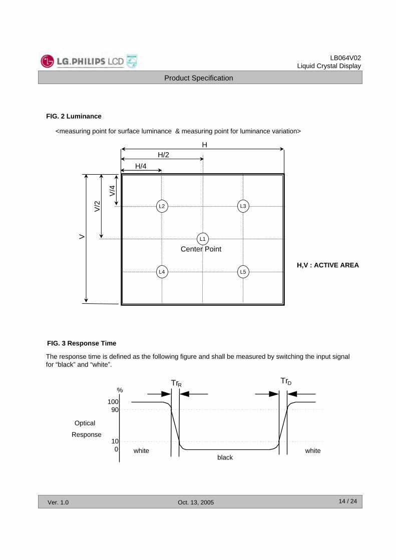
3. The variation in surface luminance , The Panel total variation (δ WHITE) is determined by measuring LNat each test position 1 through 5, and then dividing the maximum LN of 5 points luminance byminimum LN of 5 points luminance. For more information see FIG 2.
δ WHITE = Maximum(L1,L2, … L5) / Minimum(L1,L2, … L5)
4. Response time is the time required for the display to transition from white to black (rise time, TrR) andfrom black to white(Decay Time, TrD). For additional information see FIG 3.
5. Viewing angle is the angle at which the contrast ratio is greater than 5. The angles are d e t e r m i n ed for the horizontal or x axis and the vertical or y axis with respect to the z axis which is normal to theLCD surface. For more information see FIG 4.
100L6376.0L55
14.5L2325.8L3140.0L3957.0L47
5.5L151.0L70.3L0
Luminance [%] (Typ)Gray Level
6. Gray scale specification * fV=60Hz
Product Specification
14 / 24
LB064V02Liquid Crystal Display
Ver. 1.0 Oct. 13, 2005
FIG. 3 Response Time
The response time is defined as the following figure and shall be measured by switching the input signal for “black” and “white”.
TrR TrD
10090
100
%
Optical
Response
whiteblack
white
FIG. 2 Luminance
<measuring point for surface luminance & measuring point for luminance variation>
H
V
V/4
H,V : ACTIVE AREAL4 L5
L1
L2 L3
Center Point
V/2
H/4H/2

Product Specification
15 / 24
LB064V02Liquid Crystal Display
Ver. 1.0 Oct. 13, 2005
FIG. 4 Viewing angle
<Dimension of viewing angle range>
z’ yd
xr
φ
θ= 0˚zφ= 90˚
(12:00)yu
θ
φ= 0˚(3:00)
φ = 180˚(9:00)
xl
φ= 270˚(6:00)
TFT LCDMODULE

Product Specification
16 / 24
LB064V02Liquid Crystal Display
Ver. 1.0 Oct. 13, 2005
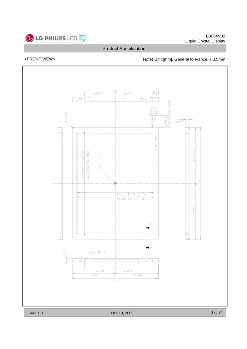
7. Mechanical CharacteristicsThe contents provide general mechanical characteristics for the model LB064V02. In addition the figuresin the next page are detailed mechanical drawing of the LCD.
97.92 (± 0.5) mmVertical
130g (TYP), 140g(MAX)Weight
111.5 (± 0.5)mmVertical
6 (± 0.3)mmDepth
130.56 (± 0.5) mmHorizontalActive Display Area
145.5 (± 0.5)mmHorizontal
Outline Dimension
Product Specification
17 / 24
LB064V02Liquid Crystal Display
Ver. 1.0 Oct. 13, 2005
<FRONT VIEW> Note) Unit:[mm], General tolerance: ± 0.5mm

Product Specification
18 / 24
LB064V02Liquid Crystal Display
Ver. 1.0 Oct. 13, 2005
<REAR VIEW> Note) Unit:[mm], General tolerance: ± 0.5mm
Product Specification
19 / 24
LB064V02Liquid Crystal Display
Ver. 1.0 Oct. 13, 2005
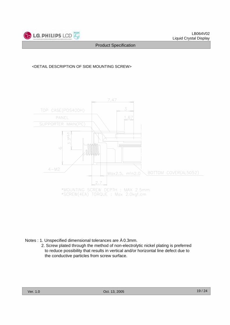
<DETAIL DESCRIPTION OF SIDE MOUNTING SCREW>
Notes : 1. Unspecified dimensional tolerances are ±0.3mm.2. Screw plated through the method of non-electrolytic nickel plating is preferred
to reduce possibility that results in vertical and/or horizontal line defect due tothe conductive particles from screw surface.
Product Specification
20 / 24
LB064V02Liquid Crystal Display
Ver. 1.0 Oct. 13, 2005
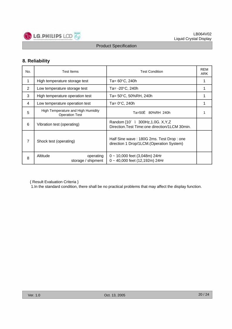
8. Reliability
{ Result Evaluation Criteria }1.In the standard condition, there shall be no practical problems that may affect the display function.
1Ta=50℃ 80%RH 240hHigh Temperature and High Humidity Operation Test5
0 ~ 10,000 feet (3,048m) 24Hr0 ~ 40,000 feet (12,192m) 24Hr
Half Sine wave : 180G 2ms. Test Drop : one direction 1 Drop/1LCM.(Operation System)
Random [10㎐↔300Hz,1.0G. X,Y,Z Direction.Test Time:one direction/1LCM 30min.
Ta= 0°C, 240h
Ta= 50°C, 50%RH, 240h
Ta= -20°C, 240h
Ta= 60°C, 240h
Test Condition
1
1
1
1
REMARK
Vibration test (operating)6
Altitude operatingstorage / shipment8
Shock test (operating)7
Low temperature operation test4
High temperature operation test3
Low temperature storage test2
High temperature storage test1
Test ItemsNo.

Product Specification
21 / 24
LB064V02Liquid Crystal Display
Ver. 1.0 Oct. 13, 2005
9. International Standards
9-1. Safety
a) UL 60950-1:2003, First Edition, Underwriters Laboratories, Inc.,Standard for Safety of Information Technology Equipment.b) CAN/CSA C22.2, No. 60950-1-03 1st Ed. April 1, 2003, Canadian Standards Association,Standard for Safety of Information Technology Equipment.c) EN 60950-1:2001, First Edition, European Committee for Electro technical Standardization(CENELEC)European Standard for Safety of Information Technology Equipment.
9-2. EMC
a) ANSI C63.4 “Methods of Measurement of Radio-Noise Emissions from Low-Voltage Electrical and Electrical Equipment in the Range of 9kHZ to 40GHz. “American National Standards Institute(ANSI),1992b) C.I.S.P.R. “Limits and Methods of Measurement of Radio Interface Characteristics of InformationTechnology Equipment.“ International Special Committee on Radio Interference.c) EN 55022 “Limits and Methods of Measurement of Radio Interface Characteristics of InformationTechnology Equipment.“ European Committee for Electro technical Standardization.(CENELEC), 1998( Including A1: 2000 )
Product Specification
22 / 24
LB064V02Liquid Crystal Display
Ver. 1.0 Oct. 13, 2005
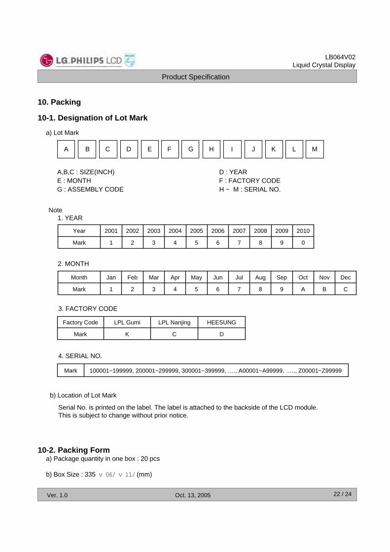
10-2. Packing Forma) Package quantity in one box : 20 pcs
b) Box Size : 335 x 281 x 331 (mm)
10. Packing
10-1. Designation of Lot Mark
a) Lot Mark
A B C D E F G H I J K L M
A,B,C : SIZE(INCH) D : YEAR E : MONTH F : FACTORY CODEG : ASSEMBLY CODE H ~ M : SERIAL NO.
Note1. YEAR
2. MONTH
4. SERIAL NO.
Mark
Year
0
2010
6
2006
7
2007
8
2008
9
2009
4
2004
5
2005
321
200320022001
B
Nov
Mark
Month
A
Oct
6
Jun
7
Jul
8
Aug
9
Sep
4
Apr
5
May
C321
DecMarFebJan
3. FACTORY CODE
C
LPL Nanjing
D
HEESUNG
Mark
Factory Code
K
LPL Gumi
b) Location of Lot Mark
Serial No. is printed on the label. The label is attached to the backside of the LCD module.This is subject to change without prior notice.
Mark 100001~199999, 200001~299999, 300001~399999, …., A00001~A99999, ….., Z00001~Z99999
Product Specification
23 / 24
LB064V02Liquid Crystal Display
Ver. 1.0 Oct. 13, 2005
11. PRECAUTIONS
Please pay attention to the following when you use this TFT LCD module.
11-1. MOUNTING PRECAUTIONS(1) You must mount a module using holes arranged in four corners or four sides.(2) You should consider the mounting structure so that uneven force(ex. Twisted stress) is not applied
to the module.And the case on which a module is mounted should have sufficient strength so that external forceis not transmitted directly to the module.
(3) Please attach a transparent protective plate to the surface in order to protect the polarizer.Transparent protective plate should have sufficient strength in order to the resist external force.
(4) You should adopt radiation structure to satisfy the temperature specification.(5) Acetic acid type and chlorine type materials for the cover case are not desirable because the former
generates corrosive gas of attacking the polarizer at high temperature and the latter causes circuitbreak by electro-chemical reaction.
(6) Do not touch, push or rub the exposed polarizers with glass, tweezers or anything harder than HBpencil lead. And please do not rub with dust clothes with chemical treatment.Do not touch the surface of polarizer for bare hand or greasy cloth.(Some cosmetics deterioratethe polarizer.)
(7) When the surface becomes dusty, please wipe gently with absorbent cotton or other soft materialslike chamois soaks with petroleum benzine. Normal-hexane is recommended for cleaning theadhesives used to attach front / rear polarizers. Do not use acetone, toluene and alcohol becausethey cause chemical damage to the polarizer.
(8) Wipe off saliva or water drops as soon as possible. Their long time contact with polarizer causesdeformations and color fading.
(9) Do not open the case because inside circuits do not have sufficient strength. (10) The metal case of a module should be contacted to electrical ground of your system.
11-2. OPERATING PRECAUTIONS
(1) The spike noise causes the mis-operation of circuits. It should be lower than following voltage :V=±200mV(Over and under shoot voltage)
(2) Response time depends on the temperature.(In lower temperature, it becomes longer.)(3) Brightness depends on the temperature. (In lower temperature, it becomes lower.)
And in lower temperature, response time(required time that brightness is stable after turned on)becomes longer.
(4) Be careful for condensation at sudden temperature change. Condensation makes damage topolarizer or electrical contacted parts. And after fading condensation, smear or spot will occur.
(5) When fixed patterns are displayed for a long time, remnant image is likely to occur.(6) Module has high frequency circuits. Sufficient suppression to the electromagnetic interference
shall be done by system manufacturers. Grounding and shielding methods may be important tominimized the interference.
Product Specification
24 / 24
LB064V02Liquid Crystal Display
Ver. 1.0 Oct. 13, 2005
Since a module is composed of electronic circuits, it is not strong to electrostatic discharge. Make certainthat treatment persons are connected to ground through wrist band etc. And don’t touch interface pin directly.
11-3. ELECTROSTATIC DISCHARGE CONTROL
Strong light exposure causes degradation of polarizer and color filter.
11-4. PRECAUTIONS FOR STRONG LIGHT EXPOSURE
When storing modules as spares for a long time, the following precautions are necessary.(1) Store them in a dark place. Do not expose the module to sunlight or fluorescent light. Keep the
temperature between 5°C and 35°C at normal humidity.(2) The polarizer surface should not come in contact with any other object.
It is recommended that they be stored in the container in which they were shipped.
11-5. STORAGE
(1) When the protection film is peeled off, static electricity is generated between the film and polarizer.This should be peeled off slowly and carefully by people who are electrically grounded and with wellion-blown equipment or in such a condition, etc.
(2) The protection film is attached to the polarizer with a small amount of glue. If some stress is appliedto rub the protection film against the polarizer during the time you peel off the film, the glue is apt toremain on the polarizer.Please carefully peel off the protection film without rubbing it against the polarizer.
(3) When the module with protection film attached is stored for a long time, sometimes there remains avery small amount of glue still on the polarizer after the protection film is peeled off.
(4) You can remove the glue easily. When the glue remains on the polarizer surface or its vestige isrecognized, please wipe them off with absorbent cotton waste or other soft material like chamoissoaked with normal-hexane.
11-6. HANDLING PRECAUTIONS FOR PROTECTION FILM

Our company network supports you worldwide with offices in Germany, Great Britain, Italy, Turkey and the
USA. For more information please contact:
Distec GmbH
Augsburger Str. 2b
82110 Germering
Germany
Phone: +49 (0)89 / 89 43 63-0
Fax: +49 (0)89 / 89 43 63-131
E-Mail: [email protected]
Internet: www.datadisplay-group.de
Display Technology Ltd.
5 The Oaks Business Village
Revenge Road, Lordswood
Chatham, Kent, ME5 8LF
United Kingdom
Phone: +44 (0)1634 / 67 27 55
Fax: +44 (0)1634 / 67 27 54
E-Mail: [email protected]
Internet: www.datadisplay-group.co.uk
Apollo Display Technologies, Corp.
87 Raynor Avenue, Unit 1Ronkonkoma, NY
11779
United States of America
Phone: +1 631 / 580-43 60
Fax: +1 631 / 580-43 70
E-Mail: [email protected]
Internet: www.datadisplay-group.com
Sales Partner: Sales Partner:
REM Italy s.a.s.
di Michieletto Flavio & C.
Via Obbia Bassa, 10
I-35010 Trebaseleghe (PD)
Italy
Phone: +39 335 521 37 89
E-Mail: [email protected]
Internet:www.remitaly.com
DATA DISPLAY BİLİŞİM TEKNOLOJİLERİ
İÇ VE DIŞ TİCARET LİMİTED ŞİRKETİ
Barbaros Mh Ak Zamabak Sk A Blok
D:143 Ataşehir/İstanbul
Turkey
Phone: +90 (0)216 / 688 04 68
Fax: +90 (0)216 / 688 04 69
E-Mail: [email protected]
Internet:www.data-display.com.tr