line to ground fault analysis of transmission line with 3
TRANSCRIPT

SSRG International Journal of Electrical and Electronics Engineering (SSRG-IJEEE) – Volume 4 Issue 5 – May 2017
ISSN: 2348 – 8379 www.internationaljournalssrg.org Page 28
Line to Ground Fault Analysis of Transmission
Line with 3 Level SVPWM Based STATCOM
for Reactive Power Management S.M.Padmaja #1, N Silpa#2
#1Professor, Department of Electrical & Electronics Engineering #2Asst. Professor, Department of Computer Science & Engineering
Shri Vishnu Engineering College for Women
Bhimavaram, Andhra Pradesh, India
Abstract The occurrence of sudden faults in a power
transmission network leads to severe short term
imbalance in the power system stability. Without
threatening the power system stability, the power
transfer capability of a transmission network can be
enhanced to its maximum limits by using Flexible AC
Transmission System (FACTS) controllers. The
application of FACTS technology through multilevel
converter topologies is attracting research interests due
to its additional benefits in improving the power
quality. Therefore, appropriate fault analysis for a
reliable multilevel converter is the prerequisite for the
realization of transmission network.
This paper is intended to investigate the
voltage profile and reactive power prevailing in the
transmission network of IEEE-14 bus system during the
weakest period of the line to ground fault. The
performance of traditional 2-level voltage source
converter is compared with that of 3- level diode
clamped multilevel converter topology through an
efficient Space Vector Pulse Width Modulation
(SVPWM) control strategy. The complete fault analysis
is verified through the simulation in MATLAB /
SIMULINK.
Keywords: 3-SVPWM, STATCOM, Multi Level Converter,
Reactive Power Management, L-G Fault.
I. INTRODUCTION
Line to Ground faults are most popular and commonly occurs in power transmission and distribution networks [1-2]. The faults involve with varying amounts of impedance. A fault with zero ground impedance is termed as short circuit with maximum fault current. Whereas, many faults are with varying ground impedance and decides the severity of the fault [3]. Various protection schemes have been involved for the safety of the equipment [4-5]. However, the most critical requirement for electrical power utilities is an uninterruptible and continuous power flow. Therefore, analysis of the faulted power system and its
influence in terms of extent of voltage sag and reactive power availability is necessary for the stable, safe and secured power system. Such demands can be met by the by the new configured applications of power electronics known as FACTS. The instantaneous voltage support and improvement of the transient stability by reactive power exchange with the power system is achieved through a Static Synchronous Compensator (STATCOM) application from FACTS family [6-7]. The STATCOM has inherent potential in giving faster response and greater output to a system with depressed voltage. For medium voltage and high power applications, reliability is a major concern and thus the concept of multilevel converters have been developed that produce a synthesized stair case voltage waveform. Compared to conventional two-level VSC, a 3-level diode clamped multilevel converter (DCMC) exhibits a promising converter topology for STATCOM applications [8-9].
The most effective way to operate the power switching devices of the 3-level STATCOM is through the implementation of SVPWM control strategy. In SVPWM technique, the combined effect of all the three output voltages of the STATCOM at the point of common coupling are considered in generating the Pulse Width Modulated switching pattern [10-11]. This unique feature helps in the complete utilization of DC voltage of the STATCOM unlike with other PWM techniques.
In this paper SVPWM control scheme is implemented on 2-level VSC and 3-level DCMC based STATCOM for the case of single line to ground fault on an IEEE-14 bus system under non linear load conditions. The bulk power systems like IEEE-14 bus network need active power flow control also for better performance along with reactive power control. So the authors in this paper concentrated on both the STATCOM and Multi Level STATCOM integrated with and without energy storage device. As case one, the STATCOM is chosen to be optimally located at bus-14 with the fault at bus-3 and their simultaneous impact on all other buses is analyzed [15-16]. In case two, the fault is considered near the STATCOM in the line 12-13. The

SSRG International Journal of Electrical and Electronics Engineering (SSRG-IJEEE) – Volume 4 Issue 5 – May 2017
ISSN: 2348 – 8379 www.internationaljournalssrg.org Page 29
IEEE-14 bus system with its standard data is shown figure 1.
Figure 1. IEEE 14 – Bus System
II. STATCOM MODEL
The STATCOM is generally connected to an AC utility bus by means of a coupling phase shifting transformer. The other side of the STATCOM is connected to a capacitor that carries the DC voltage Vdc. The STATCOM balances the output three phase sinusoidal voltages by maintaining the power equality constraint on both sides [12-13]. A loop equation is written involving the AC side phase voltages and the internal STATCOM series resistance and leakage inductance of the coupling transformer [14].
eabcs = Rsiabcs + Ls d
dt iabcs + Vabcl (1)
Where eabcs , Vabcl , iabcs are the three phase quantities expressed as [3x1] matrices and Rs , Ls , are the diagonal matrices as shown below.
eabcs =
eas
ebs
ecs
;
Vabcl =
val
vbl
vcl
;
iabcs = ias
ibs
ics
Where, Rs=
Rs 0 00 Rs 00 0 Rs
and
Ls = Ls 0 00 Ls 00 0 Ls
The AC output of the STATCOM (neglecting harmonics) is expressed in terms of DC voltage as given in equation (2),
eas
ebs
ecs
= 1
3 M
vdc
sin θ(t)
sin(θ t −2π
3 )
sin(θ t +2π
3 )
(2)
Where, θ t = ωt + α
M and θ are the amplitude modulation Index (M.I) and angle modulation index respectively.
vdc is the DC bus voltage and ω is the system frequency.
The dynamic response of the STATCOM is proportional to the real and reactive power exchange between the STATCOM and the utility system which is controlled through the direct (Id) and quadrature axis (Iq) current components respectively. Thus, it is desirable to transfer the parameters in the abc frame to the dqo frame through the transformation matrix k [10] as given in equation (3).
K =2
3
cos θs cos(θs −
2π
3) cos(θs +
2π
3)
sin θs sin(θs −2π
3) sin(θs +
2π
3)
12
12
12
(3)

SSRG International Journal of Electrical and Electronics Engineering (SSRG-IJEEE) – Volume 4 Issue 5 – May 2017
ISSN: 2348 – 8379 www.internationaljournalssrg.org Page 30
The DC side circuit of the STATCOM is expressed as,
d
dt(
vdc
2) =
1
C idc (4)
The DC current idc is related to AC phase currents [ iabcs ] at the STATCOM terminal.
idc =−1
3 M
ias
ibs
ics
sin θm
sin(θm −2π
3)
sin(θm +2π
3)
(5)
The d and q axis voltage equations of the STATCOM connected at the AC side load terminals are shown in equations (6) and (7) in which the d and q current components are also coupled.
vds = vml + Rsids + Ls
d
dt ids − Lsωiqs 6
vqs = Rsiqs + Ls
d
dt iqs + Lsωids 7
Based on above equations (6) and (7), the amplitude and angle modulation index of the resultant vector are calculated from equations (8) and (9),
M= 3
vdc vds
2 + vqs2 =
3
vdcVref (8)
α = tan−1vqs
vds 9
III. SVPWM CONTROL STRATEGY
The SVPWM control methodology is extended from a traditional 2-level STATCOM to a 3-level diode clamped multilevel converter based STATCOM. SVPWM control scheme creates an efficient gate pulse pattern for multilevel converter. A reference space vector is generated from the combined effect of three phase output voltages to create the desired sinusoidal shaped waveform. SVPWM technique is made suitable for high voltage and high power application as it shows relatively good utilization of the DC link voltage. However, as the number of levels increase, the redundancy with the switching state increases. So it is important to balance between losses and the selection of multilevel converter levels for certain applications. The SVPWM technique alleviated for higher levels is same as the basic implementation of SVPWM in 2-level
VSC[11]. The steps involved for the determination of resultant reference voltage vector shown in Figure 2 is discussed in section II. The magnitude and angle of the reference space vector voltage is obtained from the parks transformation of 3∅-2∅ conversion and its amplitude and angle modulation index are obtained from equations (8) and (9).
Figure 2. Reference Voltage Space Vector
A. Switching States
In a two level VSC, the number of switching devices in each leg of the converter is two, due to which the total possible switching voltage vectors are 23=8 obtained from eight different switching combinations. Out of which two are zero vectors and six are active vectors.
In a 3-level VSC, the number of switching devices in each leg of the converter is double that of in 2-level VSC, due to which there are three different switching states for each leg and so the total number of switching voltage vectors possible are 33 = 27. With this advantage SVPWM aims to identify the nearest voltage vectors closer to the reference space vector. The three closest vectors of the commanded reference vector Vref, are usually used to synthesis Vref.
The three different switching states denoted as 1, 0 and -1 developed three levels of resultant line voltages as 1/2Vdc, 0, -1/2Vdc . The 27 voltage vectors are classified into four groups as 3 zero voltage vectors, 12 small vectors, 6 large vectors and 6 medium voltage vectors as shown in the Table 1.
The space vector V0 is a zero vector with magnitude ‗0‘ obtained from three types of switching combinations (1 1 1), (0 0 0), (-1 -1 -1). Certain switching combinations like V1: (1 0 0), (0 -1 -1); V2 : (1 1 0), (0 0 -1); V3 : (0 1 0), (-1 0 -1); V4 : (0 1 1), (-1 0 0); V5 : (0 0 1), (-1 -1 0); V6 : (1 0 1), (0 -1 0); produce a magnitude of 1/3 Vdc and considered as small vectors.

SSRG International Journal of Electrical and Electronics Engineering (SSRG-IJEEE) – Volume 4 Issue 5 – May 2017
ISSN: 2348 – 8379 www.internationaljournalssrg.org Page 31
Each small vector is obtained from two different switching combinations. The voltage vectors with magnitude 2/3 Vdc come under large vectors obtained from the switching combinations V7: (1 -1 -1); V9: (1 1 -1); V11: (-1 1 -1); V13: (-1 1 1); V15: (-1 -1 1); V17: (1 -1
1). 1
3Vdc is the magnitude of medium vector which is midway
between small and large vectors obtained from the switvhing combinations of V8 : (1 0 -1); V10 : (0 1 -1); V12 : (-1 1 0); V14 : (-1 0 1); V16 : (0 -1 1); V18 : (1 -1 1).
Table 1. Magnitude of 27 Voltage Vectors and Their Switching State
No. of
Switching state Switching State
Space
Vector Angle Vector Type Magnitude
No. of Switching
combinations
1 1 1 1
V0
0
Zero 0 3 2 0 0 0
3 -1 -1 -1
4 1 0 0 V1
0
Small Vector
1
3Vdc 2
5 0 -1 -1
6 1 1 0 V2
𝜋
3 1
3Vdc 2
7 0 0 -1
8 0 1 0 V3
2𝜋
3 1
3Vdc 2
9 -1 0 -1
10 0 1 1 V4
𝜋 1
3Vdc 2
11 -1 0 0
12 0 0 1 V5
4𝜋
3 1
3Vdc 2
13 -1 -1 0
14 1 0 1 V6
5π
3 1
3Vdc 2
15 0 -1 0
16 1 -1 -1 V7 0
Large Vector
2
3Vdc 1
17 1 1 -1 V9 π
3
2
3Vdc 1
18 -1 1 -1 V11 2π
3
2
3Vdc 1
19 -1 1 1 V13 𝜋 2
3Vdc 1
20 -1 -1 1 V15 4π
3
2
3Vdc 1
21 1 -1 1 V17 5π
3
2
3Vdc 1
22 1 0 -1 V8 π
6
Medium
Vector
1
3Vdc 1
23 0 1 -1 V10 π
2
1
3Vdc 1
24 -1 1 0 V12 5π
6
1
3Vdc 1
25 -1 0 1 V14 −5π
6
1
3Vdc 1
26 0 -1 1 V16 −π
2
1
3Vdc 1
27 1 -1 1 V18 −π
6
1
3Vdc 1

SSRG International Journal of Electrical and Electronics Engineering (SSRG-IJEEE) – Volume 4 Issue 5 – May 2017
ISSN: 2348 – 8379 www.internationaljournalssrg.org Page 32
B. Space Vector Diagram
The 27 space voltage vectors are represented in a hexagon plane formed by 6 sectors, with each sector sub divided into 4 regions 1, 2, 3 and 4 as shown in Figure 3. For example, if the reference vector is in sector 1 and region 3, the three nearest voltage vectors are V1, V2 and V8. V1 is obtained with a two different switching states i.e., (100), (0-1-1). Similarly V2 is obtained with (00-1)(110) and V8 by the voltage vector (10-1). That means there exists different switching states for the same voltage level as for the case of V0 and V2. Such non-zero vectors are called small vectors pointing to the vertices of the inner hexagon. The three phase voltage levels obtained from the non-zero voltage
vectors are 2
3Vdc,
1
3 Vdc and
1
3Vdc.
Figure 3. Switching state vectors of 3 –level VSI
represented in Hexagon model
C. Determination of Sector and Region
The position of the reference vector in any sector is identified by the angle modulation index similar to that of 2-level VSC. To identify the region of a sector in which the reference vector is placed, a simple vector resolution calculation is followed as discussed below. In Figure 4 each side of the region is considered as unity and the reference vector mn is resolved into m1
and m2. The phasor resolution is re-presented in Figure 5. Based on the magnitude of m1 and m2, the placement of the reference vector is determined. Relevant equations for the calculation of m1 and m2 are discussed below.
p
sinπ2
= q
sinπ3
(10)
Figure 4. Reference vector in region 1 of sector 1
Figure 5. Phasor resolution of reference vector
p = m2 = q2
3=
2
3mn sin α (11)
∴ m2 =2
3mn sin α (12)
m1 = mn cos α − r (13)
m1 = mn cos α − p cosπ
3 (14)
m1 = mn cos α − [(2
3mn sin α)cos
π
3] (15)
∴ m1 = mn (cos α −sin α
3) (16)
Based on the values obtained for m1 and m2 from
equations (24) and (28), the region for the location of

SSRG International Journal of Electrical and Electronics Engineering (SSRG-IJEEE) – Volume 4 Issue 5 – May 2017
ISSN: 2348 – 8379 www.internationaljournalssrg.org Page 33
reference vector is identified from the conditions shown
in Table 2.
Table 2. Conditions for the Location Reference Vector
Condition Region
m1 ≤ 1
m2 ≤ 1
m1 + m2 ≤ 1
1
m1 > 1 2
m2 ≤ 1
m2 ≤ 1
m1 + m2 > 1
3
m2 > 1 4
D. ON Tme of the Reference Vector in a Region
The ON time of the reference vector in any region of a sector is calculated by applying the volt- time rule to the three nearest voltage vectors with their respective switching times. Consider the reference vector in sector 1 and region 3 as shown in Figure 6. V1, V2 and V8 are the nearest voltage vectors with their respective switching times as Ta, Tb and Tc. Equation (17) shows the volt-time balance relationship with the respective nearest vectors values. Since V1, V2 voltage vectors are available with two switching states, proper switching pattern is followed such that, only one device operates during the switching transition from one state to other. From the switching pattern, the switching time for each switch can be determined.
V1T1 + V2T2 + V8T3 = Vref TS (17)
Figure 6. Selection of the Sequence of voltage vectors in
each region
The amplitude and the angle of the voltage vectors V1, V2, V8 are substituted from the table xx
1
3Vdc Ta +
1
3Vdc cos
π
6+ jsin
π
6 Tb +
1
3Vdc cos
π
3+ jsin
π
3 Tc =
Vref cosθ + jsinθ Ts (18)
Dividing the equation (18) into real and imaginary parts eases the calculations for the duty cycle.
Equating the real parts,
1
3Vdc Ta +
1
2Vdc Tb +
1
6Vdc Tc
= Vref cosθTs (19)
Multiplying above equation with 3
Vdc
Ta +3
2Tb +
1
2Tc
= 3Vref
VdccosθTs (20)
Equating the imaginary parts,
1
3
1
2Vdc Tb +
1
3
3
2Vdc Tc
= Vref sinθTs (21)
Multiplying above equation with 3
Vdc
3
2Tb +
3
2Tc
= 3Vref
VdcsinθTs (22)
The uniform distribution of sampling time is expressed as
TS
= Ta + Tb + Tc (23)
By solving equations (20), (22) and (23), we get
Ta
= TS 1− 2Msinθ (24)

SSRG International Journal of Electrical and Electronics Engineering (SSRG-IJEEE) – Volume 4 Issue 5 – May 2017
ISSN: 2348 – 8379 www.internationaljournalssrg.org Page 34
Tb = TS 2Msin π
3+ θ
− 1 (25)
Tc = TS 1 − 2Msin π
3+ θ (26)
Where M is the Modulation index and expressed as,
M = 3Vref
Vdc (27)
The time duration of reference vector in remaining regions of all the sectors is calculated in the similar fashion. The optimal switching pattern followed in each region is represented with respect to the ON time durations of respective switching vectors Ta, Tb, and Tc in that region. Figure 7 depicts the demanded states of the upper switches of one phase S1a & S2a corresponding to Ta, Tb, Tc, in region 3 of sector 1. However, the switching states of lower switches in each phase are complement to that of their upper switches. Similar procedure is applied to decide the total switching time of each switch in the remaining regions of all the sectors. The method of generating of PWM pulses is the same as that in 2-L SVPWM. The total ON time of each switch in each region over a sampling time TS is compared with a triangle carrier to generate the SVPWM pulses.
IV. PERFORMANCE EVALUATION
In this paper, the effect of SVPWM controlled 2-Level and 3-Level DCMC based STATCOM on the stability of the power system during the line-ground fault is demonstrated. As a test model, a standard IEEE-14 bus system is considered to evaluate its performance. The optimum locations for the placement of STATCOM are chosen as the buses with least voltage and that
provide minimum losses [15-16]. Figure 1 shows the single line diagram of the IEEE-14 bus system integrated with 138KV and 100MVA STATCOM at bus-14. Two cases of location of line to ground fault is considered. One is far away at bus -3 abd other is near to bus -14 in the middle of the line 13-14, with a fault impedance of 50Ω. The digital simulation using PSB/ Simulink was performed. The simulation results of 2 level and 3 level STATCOM reactive current components, DC capacitor voltages, transmission line voltages, active and reactive powers and load voltages at all the buses are analyzed during the fault.
Case I: At t=0.1s to 0.12s, for the sudden line-ground fault at bus-3, the system becomes weak and the bus voltages exhibit oscillations and a high reactive power is drawn instantaneously towards bus-3. The sudden supply of adequate real and reactive power transfer in the lines near to bus-3 is adjusted with the sacrifice of a little voltage in order to maintain the system stable. Since the STATCOM is not supported by any energy storage device and is placed far away at weak bus-14, it is not feasible to supply adequate reactive power from the STATCOM through all the lines towards bus-3. But, it helps in the increase of required reactive power drawn towards bus-3 with decrease in active power in the lines connected to bus-3. As the source is near to the fault compared to the location of STATCOM, the active and reactive powers are drawn from the nearby buses to maintain the stability of the system.
In this process there is an instantaneous dip in voltage at the starting of the fault and with the impact of STATCOM at bus-14, there is quick recovery of the voltage without losing the stability of the system. However, if the STATCOM is located at the vicinity of bus-3 itself, the amount of disturbance in voltage, real and reactive power transfer is reduced. The dynamic and stable response of the 3-level DCMC STATCOM manages the active and reactive powers and regulates the voltage in comparatively lesser time as shown. The impact of STATCOM on all the 14 bus voltages is depicted in Table 3.

SSRG International Journal of Electrical and Electronics Engineering (SSRG-IJEEE) – Volume 4 Issue 5 – May 2017
ISSN: 2348 – 8379 www.internationaljournalssrg.org Page 35
Figure 7. Switching pattern for phase A voltage and demanded status of S1a and S2a
Table 3 . Bus Voltage During the Fault with and without 2 Level and 3 Level SVPWM statcom
BUS NO. Without STATCOM 2LSVP STATCOM 3LSVP STATCOM
1 0.979 0.965 0.95
2 0.95 0.938 0.928
3 0.88 0.868 0.869
4 0.913 0.905 0.91
5 0.92 0.914 0.914
6 0.964 0.96 0.96
7 0.95 0.944 0.948
8 0.975 0.961 0.968
9 0.946 0.941 0.945
10 0.941 0.938 0.94
11 0.95 0.942 0.944
12 0.95 0.95 0.954
13 0.949 0.95 0.958
14 0.934 0.97 0.99
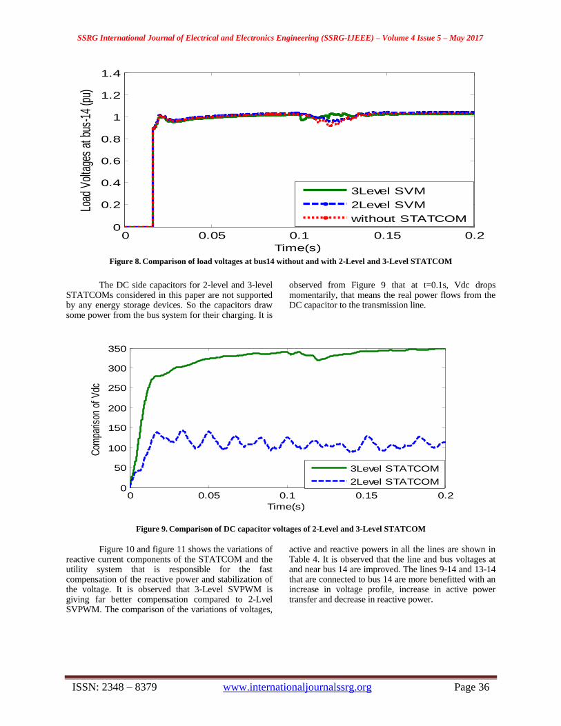
Figure 8 shows that the load voltage at bus-14 drops sharply and then slowly settles towards its normal value. Therefore, the STATCOM injects reactive power and that drawn from the source buses1 and 2 through the
neighboring lines towards bus-14 is reduced. Comparatively 3-level SVPWM STATCOM shows dynamic and fast response in settling the voltage dip to its normal value during the fault.
SSRG International Journal of Electrical and Electronics Engineering (SSRG-IJEEE) – Volume 4 Issue 5 – May 2017
ISSN: 2348 – 8379 www.internationaljournalssrg.org Page 36
Figure 8. Comparison of load voltages at bus14 without and with 2-Level and 3-Level STATCOM
The DC side capacitors for 2-level and 3-level STATCOMs considered in this paper are not supported by any energy storage devices. So the capacitors draw some power from the bus system for their charging. It is
observed from Figure 9 that at t=0.1s, Vdc drops momentarily, that means the real power flows from the DC capacitor to the transmission line.
Figure 9. Comparison of DC capacitor voltages of 2-Level and 3-Level STATCOM
Figure 10 and figure 11 shows the variations of reactive current components of the STATCOM and the utility system that is responsible for the fast compensation of the reactive power and stabilization of the voltage. It is observed that 3-Level SVPWM is giving far better compensation compared to 2-Lvel SVPWM. The comparison of the variations of voltages,
active and reactive powers in all the lines are shown in Table 4. It is observed that the line and bus voltages at and near bus 14 are improved. The lines 9-14 and 13-14 that are connected to bus 14 are more benefitted with an increase in voltage profile, increase in active power transfer and decrease in reactive power.
0 0.05 0.1 0.15 0.20
0.2
0.4
0.6
0.8
1
1.2
1.4
Time(s)
Load
Vol
tage
s at
bus
-14
(pu)
3Level SVM
2Level SVM
without STATCOM
0 0.05 0.1 0.15 0.20
50
100
150
200
250
300
350
Time(s)
Com
paris
on o
f Vdc
3Level STATCOM
2Level STATCOM

SSRG International Journal of Electrical and Electronics Engineering (SSRG-IJEEE) – Volume 4 Issue 5 – May 2017
ISSN: 2348 – 8379 www.internationaljournalssrg.org Page 37
Figure 10. STATCOM reactive current components
Figure 11. Utility reactive current components
Table 4. Voltage , Active and Reactive powers in All the Lines During the Worst Conditoin of the LG Fault
Line Voltages Active Power in MW
Reactive Power in Mvar
Line No.
without
statcom 2-Level 3-Level
without
statcom 2-Level 3-Level
Without
statcom 2-Level 3-Level
1-2 0.95 0.939 0.95 0.3975 0.40325 0.385 0.16 0.152 0.152
2-3 0.9 0.899 0.9 0.2835 0.26 0.255 0.16 0.172 0.175
1-5 0.934 0.926 0.932 0.212 0.22 0.2212 0.091 0.06975 0.06675
2-5 0.93 0.922 0.928 0.138 0.144 0.1475 0.03225 0.017 0.0187
2-4 0.93 0.922 0.928 0.153 0.16 0.163 0.0335 0.02625 0.0285
3-4 0.9 0.9 0.9 0.142 -0.1 -0.0825 -0.119 -0.165 -0.172
0 0.02 0.04 0.06 0.08 0.1 0.12 0.14 0.16 0.18 0.2-10
-5
0
5
10
15
Time(s)
ST
AT
CO
M I
q
3LSVM
2L SVM
0 0.02 0.04 0.06 0.08 0.1 0.12 0.14 0.16 0.18 0.2-60
-40
-20
0
20
Time (s)
Iqn
3LSVM
2L SVM

SSRG International Journal of Electrical and Electronics Engineering (SSRG-IJEEE) – Volume 4 Issue 5 – May 2017
ISSN: 2348 – 8379 www.internationaljournalssrg.org Page 38
4-5 0.91 0.91 0.91 0.305 0.3105 0.332 0.0786 0.05525 0.0425
7-8 0.952 0.952 0.96 0.012 0.01 0.014 -0.002 -0.005 -0.0002
7-9 0.95 0.95 0.95 0.012 0.0151 0.01595 0.00157 -0.0029 0.00058
6-11 0.95 0.95 0.95 0.035 0.0362 0.0362 0.0189 0.0187 0.0186
6-12 0.95 0.95 0.95 0.0256 0.024 0.027 0.01 0.0062 0.005
6-13 0.95 0.95 0.95 0.06 0.06 0.06 0.0267 0.0107 0.0065
9-10 0.94 0.94 0.948 0.0151 0.014 0.014 0.00035 0.0008 0.003
10-11 0.95 0.95 0.95 -0.021 -0.022 -0.0226 -0.014 -0.014 -0.0135
9-14 0.96 0.96 0.99 0.0187 0.05 0.074 0.0064 0.0049 0.0035
12-13 0.95 0.95 0.955 0.0065 0.0085 0.012 0.0026 -0.00075 -0.00285
13-14 0.95 0.962 0.98 0.0223 0.0275 0.05 0.0122 -0.006 -0.0166
Case II: The line-ground fault is considered at
t=0.1 s to o.12 s in the middle of the line 13-14 without
changing the position of the STATCOM at bus 14. Here,
the STATCOM is considered with the energy storage
device to provide performance improvement.
Occurrence of a fault suddenly draws large amounts of
line currents to satisfy the required reactive power.
Compensation of reactive power not only reduces the
losses, but also regulates the voltage stability. In the
process of controlling active and reactive power flow, in
all the lines of the system, a little voltage is needed to be
sacrificed without loosing the stability of the system.
The impact values of bus voltages and line voltages,
active powers and reactive powers by the 2-level and 3-
level SVPWM controlled STATCOM during the worst
condition of the fault period are tabulated in Table 5 and
Table 6. Undoubtedly, there is an improvement of
voltage at bus 14 that is at the point of common
coupling by 3L DCMC based STATCOM as shown in
figure 12.
Table 5. Comparison of Bus Voltages
BUS No. Without STATCOM 2LSVP at Bus 14 3LSVP at Bus 14
1 0.994 0.975 0.975
2 0.97 0.945 0.955
3 0.9305 0.911 0.93
4 0.9265 0.91 0.91
5 0.93 0.9067 0.911
6 0.974 0.952 0.957
7 0.964 0.94 0.946
8 0.9908 0.9645 0.9725
9 0.96 0.935 0.943
10 0.955 0.93 0.937
11 0.96 0.934 0.94
12 0.95 0.935 0.936
13 0.93 0.928 0.927
14 0.895 0.921 0.94
TABLE 1. COMPARISION OF LINE VOLTAGES, ACTIVE POWERS AND REACTIVE POWERS
Line Voltage in pu Active Power in pu Reactive Power in pu
Line No without 2LSVP 3LSVP without 2LSVP 3LSVP without 2LSVP 3LSVP
1-2 0.968 0.96 0.958 0.3773 0.3775 0.381 0.15 0.1439 0.14
2-3 0.942 0.928 0.92 0.209 0.203 0.209 0.0875 0.084 0.081
1-5 0.948 0.933 0.93 0.2165 0.245 0.245 0.11 0.1003 0.1

SSRG International Journal of Electrical and Electronics Engineering (SSRG-IJEEE) – Volume 4 Issue 5 – May 2017
ISSN: 2348 – 8379 www.internationaljournalssrg.org Page 39
2-5 0.944 0.93 0.925 0.16285 0.184 0.184 0.0668 0.057 0.0568
2-4 0.945 0.93 0.93 0.173 0.19 0.19 0.0643 0.0564 0.055
3-4 0.925 0.91 0.92 -0.0312 -0.017 -0.014 -0.00633 -0.007 -0.0066
4-5 0.919 0.905 0.907 0.257 0.26 0.27 0.067 0.058 0.058
7-8 0.97 0.95 0.96 0.0135 0.013 0.013 -0.0042 -0.0042 -0.0002
7-9 0.9584 0.95 0.95 0.0062 0.009 0.012 0.00687 0.005 0.0056
6-11 0.9545 0.94 0.942 0.03 0.031 0.031 0.0164 0.018 0.0161
6-12 0.95 0.94 0.94 0.0525 0.0563 0.0574 0.033 0.0288 0.0275
6-13 0.9415 0.934 0.932 0.1365 0.165 0.172 0.1635 0.15 0.146
9-10 0.95 0.935 0.94 0.0198 0.016 0.0159 0.0004 0.004 0.004
10-11 0.956 0.95 0.94 -0.0163 -0.0164 -0.0168 -0.0113 -0.0108 -0.0104
9-14 0.923 0.924 0.95 0.07 0.11 0.13 0.112 0.015 0.005
12-13 0.93 0.93 0.93 0.0323 0.039 0.04 0.035 0.028 0.025
13-14 0.865 0.906 0.92 0.0335 0.037 0.045 0.165 0.165 0.164
Also, the reactive power delivered from the source 1
during the fault period is reduced in the presence of the
STATCOM at bus 14 of the IEEE System as shown in
figure 15. With the analysis on the above results, it is
clear that the dynamic performance of the STATCOM
in the reactive power compensation during a line-ground
fault maintaining the stability of the system. In addition,
with a capacitive support at the source and load ends,
the performance at all the buses can be still improved.
Figure 12. Comparision of voltages at bus 14 under L-G
faultin line 13-14
Generally, without STATCOM, for the sudden fault in
line 13-14, the neighboring lines carry increased
Reactive Power flow obviously drown all through the
source, to supply the fault line. With STATCOM a
comparative decrease in reactive power flow is observed
in the line 9-14 connected to bus-14 as shown in figure
13.
Figure 12. Comparision of reactive power
flow in line 9-14
Figure 13. Comparision of reactive power flow in the line
12-13
0 0.05 0.1 0.15 0.20
0.2
0.4
0.6
0.8
1
1.2
1.4
Time in sec
Voltage at bus 14 in
pu
without STATCOM
with 2L SVP
with 3L SVP
0 0.05 0.1 0.15 0.2-0.05
0
0.05
0.1
0.15
Time in Sec
Lin
e 9
-14 R
eactive p
ow
er
in p
u
Without STATCOM
with 2L SVP
with 3L SVP
0 0.05 0.1 0.15 0.2-0.05
0
0.05
0.1
0.15
0.2
0.25
0.3
Time in sec
Reactive P
ow
er
of
Sourc
e1 in p
u
without STATCOM
with 2L SVP
with 3L SVP

SSRG International Journal of Electrical and Electronics Engineering (SSRG-IJEEE) – Volume 4 Issue 5 – May 2017
ISSN: 2348 – 8379 www.internationaljournalssrg.org Page 40
Simultaneously, it is also observed from figure 14, a
comparative decrease in reactive power flow in the line
12-13 which is connected to the faulty line 13-14
through bus 13.
Figure 14. Comparision of reactive power delivered
by source 1
The six sectors identified for the location of reference
vector with respective alpha variation in SVPWM
technique is shown in figure 16. Figure 17 shows the
AC output voltage of the 2-level SVPWM controlled
voltage source converter which follows the power
equality constraint with the DC side capacitor voltage of
the STATCOM supported by energy storage device.
Similarly, figure 18 shows the three levels of AC output
voltage developed by the 3-level SVPWM controlled
multi level STATCOM.
Figure 16. The six sectors identified in SVPWM technique
V. CONCLUSION
In this paper a fault compensation strategy is discussed through the implementation of 3-level DCMC and 2-level VSC based STATCOMs on the IEEE-14 bus system. Upon the occurrence of the fault, STATCOM immediately senses the severity of the fault by the error accumulation as the feedback signal. The individual switches of the converter are actively controlled by the SVPWM switching strategy. The threshold value of the error current between the STATCOM and the AC line is the feedback used for the
SVPWM controller during the fault period. The effectiveness of the SVPWM controlled 3-Level DCMC is analyzed throughout the fault period in the compensation of reactive power and to allow smooth ride through of the line and load voltages. Highest priority is given to the mitigation of the disturbance due to line-ground fault on the surrounding transmission lines and buses. From the analysis results of the simulation studies, SVPWM controlled 3-level DCMC based STATCOM shows a fault tolerant control strategy to achieve the fast and steady response in managing the
0 0.05 0.1 0.15 0.20
2
4
6
Time in sec
6 Se
ctor
s id
entif
icat
ion
wrt
alp
ha
0 0.02 0.04 0.06 0.08 0.1 0.12 0.14 0.16 0.18 0.2-4
-3
-2
-1
0
1
2
3
4
5x 10
4
Time in sec
2 L
evel S
VP
outp
ut
voltage in v
olts
0 0.02 0.04 0.06 0.08 0.1 0.12 0.14 0.16 0.18 0.2-5
-4
-3
-2
-1
0
1
2
3
4
5x 10
4
Time in sec
3Level outp
ut
voltage in v
olts
0 0.05 0.1 0.15 0.2-0.01
0
0.01
0.02
0.03
0.04
Time in sec
Reacti
ve p
ow
er i
n l
ine 1
2-1
3 i
n p
u
without STATCOM
2L SVP
3L SVP

SSRG International Journal of Electrical and Electronics Engineering (SSRG-IJEEE) – Volume 4 Issue 5 – May 2017
ISSN: 2348 – 8379 www.internationaljournalssrg.org Page 41
reactive power and voltage profile for the stable operation of the system.
REFERENCES
[1] Dr. Guenter Kiessling, Stefan Schwabe, Dr. Juergen Holbach, ―Power System Fault Analysis using Fault Reporting Data of Numerical Relays‖ Siemens PT&D.
[2] J. Beiza, S. H. Hosseinian and B. Vahidi, ―Fault Type Estimation in Power Systems‖ Iranian Journal of Electrical & Electronic Engineering, Vol. 5, No. 3, Sep. 2009.
[3] M. Sushama, G. Tulasi Ram Das and A. Jaya Laxmi, ―Detection of High-Impedance Faults In Transmission Lines Using Wavelet Transform‖, VOL. 4, NO. 3, MAY 2009 ISSN 1819-6608 ARPN Journal of Engineering and Applied Sciences ©2006-2009.
[4] Yeong Jia Cheng, Eng Kian Kenneth Sng, ―Transient Analysis and Fault Compensation During Module Failure in Paralleled Power Modules‖ IEEE TRANSACTIONS ON INDUSTRY APPLICATIONS, VOL. 42, NO. 2, MARCH/APRIL 2006.
[5] M.Sushama, Dr. G.Tulasi Ram Das, ―Detection and Classification of Voltage Sags using adaptive decomposition and wavelet transform‖ Int.j. Elect.Power Eng.,3(1):2009, Medwell Journals.
[6] N. G. Hingorani and L. Gyugyi, ―Understanding FACTS, Concepts, and Technology of Flexible AC Transmission Systems‖, Piscataway, NJ: IEEE Press, 2000.
[7] Ying Xiao, Y. H. Song, Chen-Ching Liu, Fellow, Y. Z. Sun, ―Available transfer capability enhancement using FACTS devices‖ IEEE Trans. on Power Syst., vol. 18, no. 1, february 2003
[8] K Haritha, S Kumar, Dr.Venugopal, ―Design and Operation of an improved hybrid DSTATCOM topology to compensate reactive and harmonics loads‖ SSRG International Journal of Electrical and Electronics Engineering (SSRG-IJEEE) – volume 2 Issue 3 March 2015
[9] Satish Bhakar, Ahamed Khan, Manish Kumar Bissu, Anurag Singh, ―Facts Devices and their Controlling‖ SSRG International Journal of Electrical and Electronics Engineering (SSRG-IJEEE) – volume 3 Issue 5 May 2016
[10] Tarlochan Singh Sidhu, , Rajiv K. Varma, Pradeep Kumar Gangadharan, Fadhel Abbas Albasri, , and German Rosas Ortiz, ―Performance of Distance Relays on Shunt—FACTS Compensated Transmission Lines‖ IEEE TRANSACTIONS ON POWER DELIVERY, VOL. 20, NO. 3, JULY 2005
[11] Jin-Woo Jung, ―Project#2 Space Vector PWM Inverter‖ Department of Electrical and Computer Engineering, The Ohio State University.
[12] Dong Myung Lee, JinWoo Jung, SangShin Kwak ―Simple space vector PWM scheme for three level NPC Inverters including the overmodulation region‖, Journal of power Electronics Vol.11, No.5, September 2011.
[13] M. S. ElMoursi, Prof. Dr. A. M. Sharaf, ―Voltage stabilization and reactive compensation using a novel FACTS- STATCOM scheme‖ 0-7803-8886-0/05/$20.00 ©2005 IEEE CCECE/CCGEI, Saskatoon, May 2005
[14] Amir H. Norouzi and A. M. Sharaf, ―Two Control Schemes to Enhance the Dynamic Performance of the STATCOM and SSSC‖ IEEE TRANSACTIONS ON POWER DELIVERY, VOL. 20, NO. 1, JANUARY 2005
[15] Maryam Saeedifard, Hassan Nikkhajoei, and Reza Iravani, ―A Space Vector Modulated STATCOM Based on a Three-Level Neutral Point Clamped Converter‖, IEEE TRANSACTIONS ON POWER DELIVERY, VOL. 22, NO. 2, APRIL 2007
[16] M.Arun Bhaskar, M.Mahesh, Dr.S.S.Dash, M.Jagadeesh Kumar, C.Subramani, ―Modelling and Voltage Stability Enhancement of IEEE 14 Bus System Using ―Sen‖ Transformer‖, 2011 International Conference on Signal, Image Processing and Applications, With workshop of ICEEA 2011, IPCSIT vol.21 (2011) © IACSIT Press, Singapoor.
[17] Antonio J. Conejo, Francisco D. Galiana, Ivana Kockar, ― Z-Bus Loss Allocation‖, IEEE transactions on power systems, vol.16, no.1, February 2001.