linear equivalent circuits - mit opencourseware...linear equivalent circuits: after biasing each...
TRANSCRIPT

6.012 - Microelectronic Devices and Circuits Lecture 13 - Linear Equivalent Circuits - Outline
• Announcements Exam Two -Coming next week, Nov. 5, 7:30-9:30 p.m.
• Review - Sub-threshold operation of MOSFETs
• Review - Large signal models, w. charge stores p-n diode, BJT, MOSFET (sub-threshold and strong inversion)
• Small signal models; linear equivalent circuitsGeneral two, three, and four terminal devices pn diodes: Linearizing the exponential diode
Adding linearized charge stores
BJTs: Linearizing the F.A.R. β-model Adding linearized charge stores
MOSFETs: Linearized strong inversion model Linearized sub-threshold model Adding linearized charge stores
Clif Fonstad, 10/27/09 Lecture 13 - Slide 1
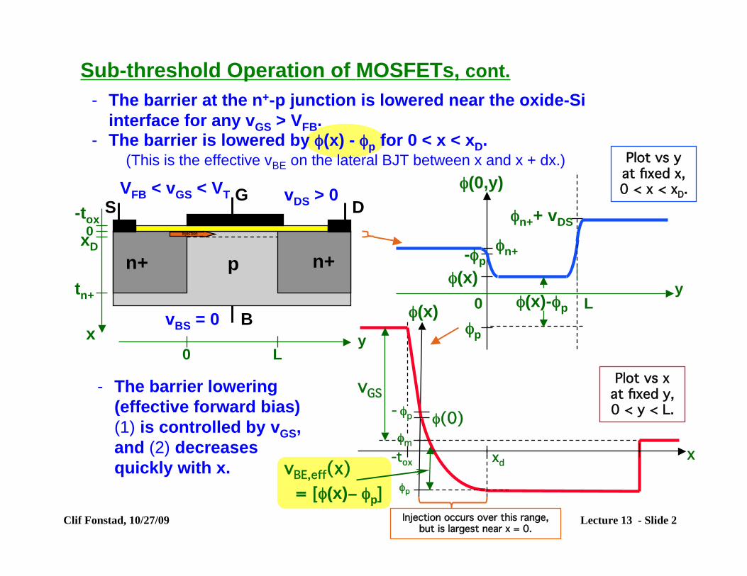
Sub-threshold Operation of MOSFETs, cont. - The barrier at the n+-p junction is lowered near the oxide-Si
Clif Fonstad, 10/27/09 Lecture 13 - Slide 2
interface for any vGS > VFB. - The barrier is lowered by φ(x) - φp for 0 < x < xD.
(This is the effective vBE on the lateral BJT between x and x + dx.)
- The barrier lowering (effective forward bias) (1) is controlled by vGS, and (2) decreases quickly with x.
D
B
S G
n+ n+ p tn+
x y0 L
vBS = 0
xD
y
φn+
φp
0 L φ(x)
φ(x)-φp
-φp
φp
-tox xxd
φm
vGS - φp φ(0)
vBE,eff(x) = [φ(x)− φp]
Plot vs x at fixed y, 0 < y < L.
φ(x)
Injection occurs over this range, but is largest near x = 0.
-tox 0
vDS > 0
Injection
VFB < vGS < VT
Plot vs y at fixed x, 0 < x < xD. φ(0,y)
φn++ vDS
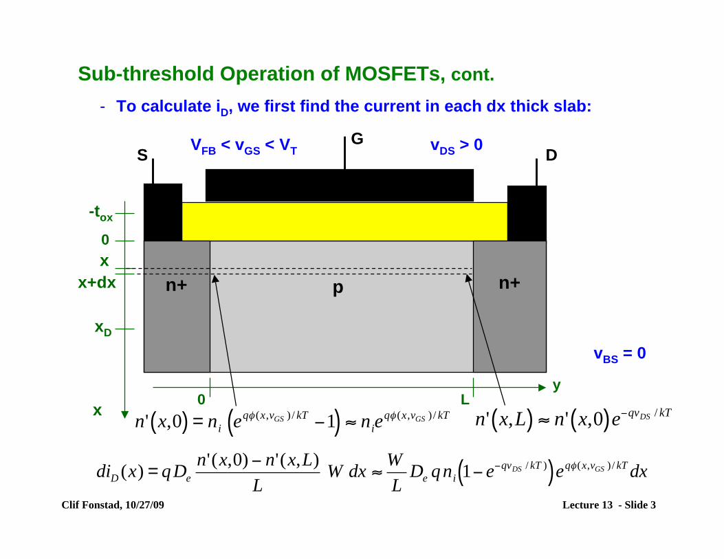
Sub-threshold Operation of MOSFETs, cont. - To calculate iD, we first find the current in each dx thick slab:
DS G
-tox
0
x y
0 L
vDS > 0
xD
VFB < vGS < VT
n+ n+ p x
x+dx
!
n' x,0( ) = ni eq" (x,vGS ) / kT #1( ) $ nie
q" (x,vGS ) / kT
!
n' x,L( ) " n' x,0( )e#qvDS / kT
vBS = 0
!
diD (x) = qDe
n'(x,0) " n'(x,L)
LW dx #
W
LDe qni 1" e
"qvDS / kT )( )eq$ (x,vGS ) / kT
dx
Clif Fonstad, 10/27/09 Lecture 13 - Slide 3
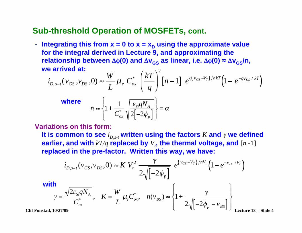
Sub-threshold Operation of MOSFETs, cont. - Integrating this from x = 0 to x = xD using the approximate value
for the integral derived in Lecture 9, and approximating the relationship between Δφ(0) and ΔvGS as linear, i.e. Δφ(0) ≈ ΔvGS/n, we arrived at:
!
iD, s"t(vGS ,vDS ,0) #W
Lµ e Cox
* kT
q
$
% &
'
( )
2
n "1[ ] eq vGS "VT{ } nkT
1" e"qvDS / kT( )
!
n " 1+1
Cox
*
#SiqNA
2 $2%p[ ]& ' (
) (
* + (
, ( =-
where
Variations on this form: It is common to see iD,s-t written using the factors K and γ we defined earlier, and with kT/q replaced by Vt, the thermal voltage, and [n -1] replaced in the pre-factor. Written this way, we have:
Clif Fonstad, 10/27/09 Lecture 13 - Slide 4 !
iD,s" t (vGS,vDS ,0) # K Vt
2 $
2 "2%p[ ]e
vGS "VT{ } nVt 1" e"vDS /Vt( )
!
" #2$SiqNA
Cox
*, K #
W
LµeCox
*, n(vBS ) % 1+
"
2 &2'p & vBS[ ]
( ) *
+ *
, - *
. *
with
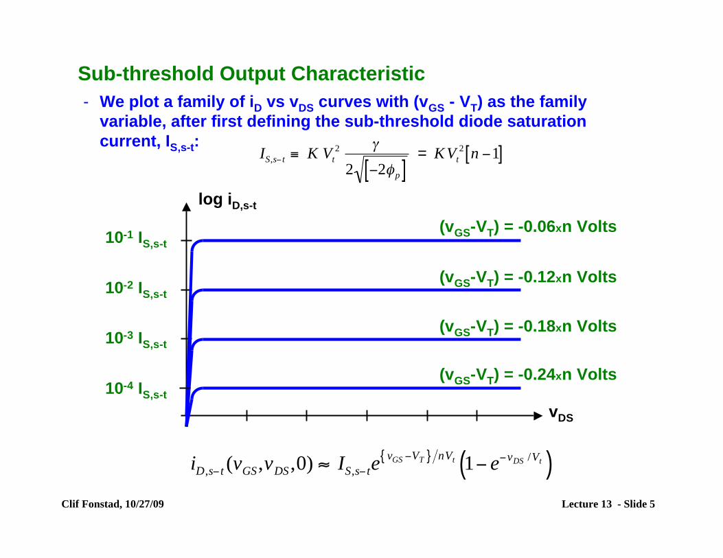
Sub-threshold Output Characteristic - We plot a family of iD vs vDS curves with (vGS - VT) as the family
variable, after first defining the sub-threshold diode saturation current, IS,s-t:
!
IS,s" t # K Vt
2 $
2 "2%p[ ]= KVt
2n "1[ ]
log iD,s-t
vDS
10-1 IS,s-t
10-2 IS,s-t
10-3 IS,s-t
10-4 IS,s-t
(vGS-VT) = -0.06xn Volts
(vGS-VT) = -0.12xn Volts
(vGS-VT) = -0.18xn Volts
(vGS-VT) = -0.24xn Volts
!
iD,s" t (vGS,vDS ,0) # IS,s" tevGS "VT{ } nVt 1" e
"vDS /Vt( )Clif Fonstad, 10/27/09 Lecture 13 - Slide 5
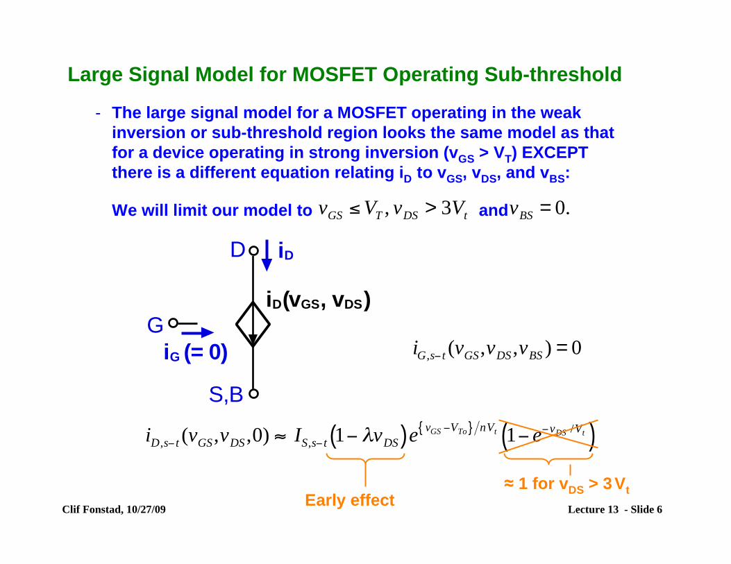
Large Signal Model for MOSFET Operating Sub-threshold
- The large signal model for a MOSFET operating in the weak inversion or sub-threshold region looks the same model as that for a device operating in strong inversion (vGS > VT) EXCEPT there is a different equation relating iD to vGS, vDS, and vBS:
We will limit our model to and
!
vGS "VT , vDS > 3Vt vBS = 0.
!
iD,s" t (vGS,vDS ,0) # IS,s" t 1" $vDS( )evGS "VTo{ } nVt 1" e
"vDS /Vt( )!
iG,s" t (vGS,vDS ,vBS ) = 0
≈ 1 for vDS > 3 Vt
G
S,B
D
iD(vGS, vDS)
iG (= 0)
iD
Early effect Clif Fonstad, 10/27/09 Lecture 13 - Slide 6
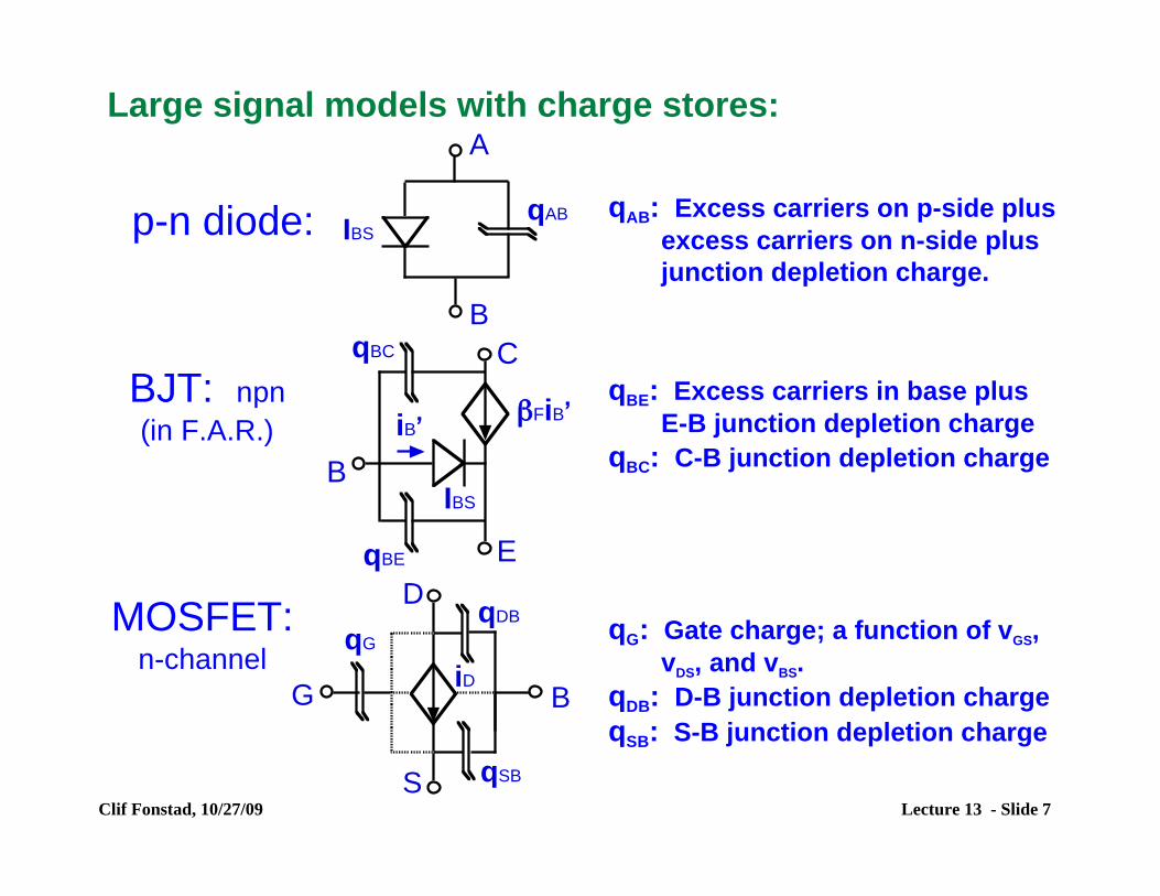
Large signal models with charge stores:
p-n diode:
BJT: npn (in F.A.R.)
MOSFET: n-channel
Clif Fonstad, 10/27/09
G
S
D qDB
iD
B
qSB
qG
qBC
B
E
C
iB’
IBS
!FiB’
qBE
B
A
IBS
qAB qAB: Excess carriers on p-side plus excess carriers on n-side plus junction depletion charge.
qBE: Excess carriers in base plus E-B junction depletion charge
qBC: C-B junction depletion charge
qG: Gate charge; a function of vGS, vDS, and vBS.
qDB: D-B junction depletion charge qSB: S-B junction depletion charge
Lecture 13 - Slide 7
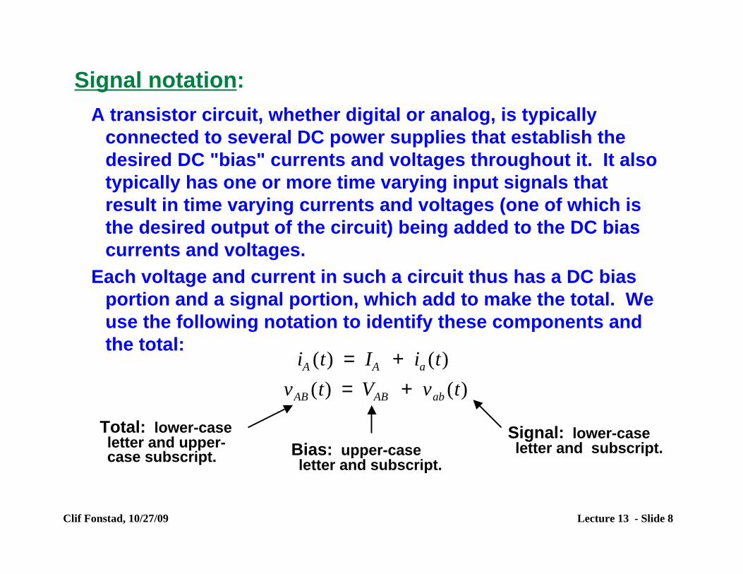
Signal notation: A transistor circuit, whether digital or analog, is typically
connected to several DC power supplies that establish the desired DC "bias" currents and voltages throughout it. It also typically has one or more time varying input signals that result in time varying currents and voltages (one of which is the desired output of the circuit) being added to the DC bias currents and voltages.
Each voltage and current in such a circuit thus has a DC bias portion and a signal portion, which add to make the total. We use the following notation to identify these components and the total:
Total: lower-case
!
iA (t) = IA + ia (t)
vAB (t) = VAB + vab (t)
Signal: lower-case letter and upper- Bias: upper-case letter and subscript. case subscript. letter and subscript.
Clif Fonstad, 10/27/09 Lecture 13 - Slide 8
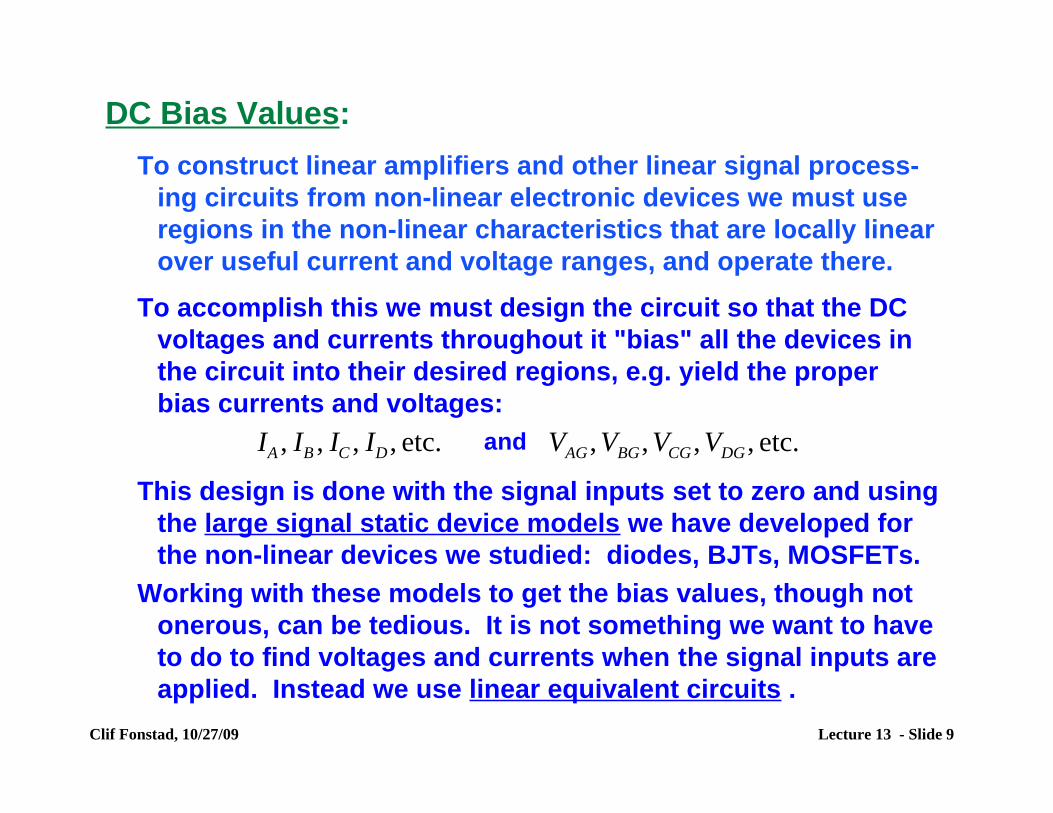
DC Bias Values: To construct linear amplifiers and other linear signal process-
ing circuits from non-linear electronic devices we must use regions in the non-linear characteristics that are locally linear over useful current and voltage ranges, and operate there.
To accomplish this we must design the circuit so that the DC voltages and currents throughout it "bias" all the devices in the circuit into their desired regions, e.g. yield the proper bias currents and voltages:
!
IA , IB , IC , ID , etc. VAG ,VBG,VCG ,VDG, etc.and
This design is done with the signal inputs set to zero and using the large signal static device models we have developed for the non-linear devices we studied: diodes, BJTs, MOSFETs.
Working with these models to get the bias values, though not onerous, can be tedious. It is not something we want to have to do to find voltages and currents when the signal inputs are applied. Instead we use linear equivalent circuits .
Clif Fonstad, 10/27/09 Lecture 13 - Slide 9
Linear equivalent circuits: After biasing each non-linear devices at the proper point the
signal currents and voltages throughout the circuit will be linearly related for small enough input signals. To calculate how they are related, we make use of the linear equivalent circuit (LEC) of our circuit.
The LEC of any circuit is a combination of linear circuit elements (resistors, capacitors, inductors, and dependent sources) that correctly models and predicts the first-order changes in the currents and voltages throughout the circuit when the input signals change.
A circuit model that represents the proper first order linear relationships between the signal currents and voltages in a non-linear device is call an LEC for that device.
Our next objective is to develop LECs for each of the non-linear devices we have studied: diodes, BJTs biased in their forward active region (FAR), and MOSFETs biased in their sub-threshold and strong inversion FARs.
Clif Fonstad, 10/27/09 Lecture 13 - Slide 10
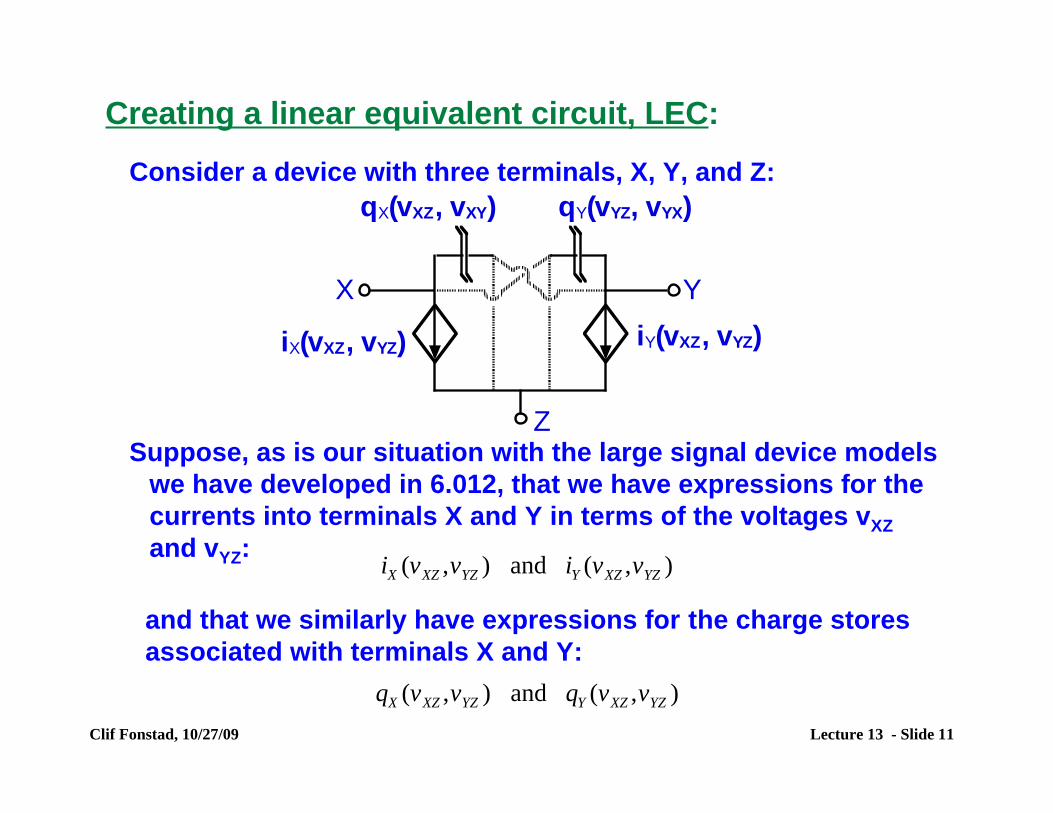
Creating a linear equivalent circuit, LEC:
YX
Z
qX(vXZ, vXY) qY(vYZ, vYX)
iX(vXZ, vYZ) iY(vXZ, vYZ)
Consider a device with three terminals, X, Y, and Z:
Suppose, as is our situation with the large signal device models we have developed in 6.012, that we have expressions for the currents into terminals X and Y in terms of the voltages vXZ and vYZ:
!
iX (vXZ ,vYZ ) and iY (vXZ ,vYZ )
and that we similarly have expressions for the charge stores associated with terminals X and Y:
!
qX (vXZ ,vYZ ) and qY (vXZ ,vYZ )
Clif Fonstad, 10/27/09 Lecture 13 - Slide 11
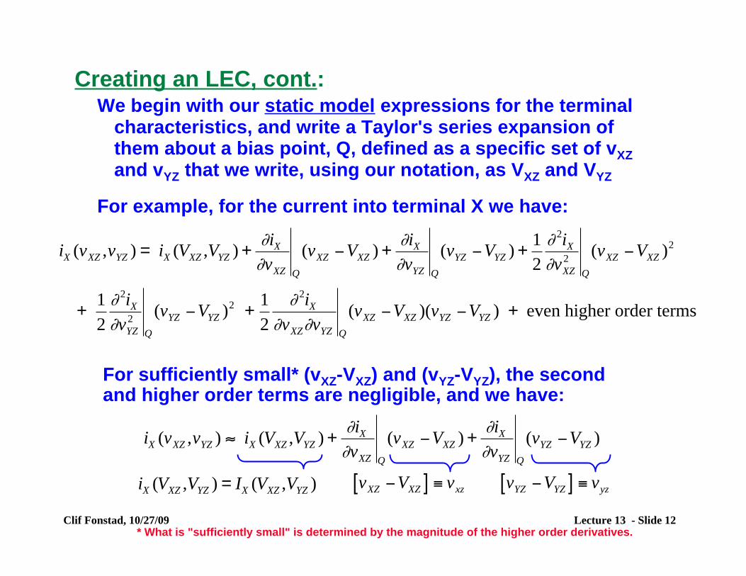
Creating an LEC, cont.: We begin with our static model expressions for the terminal
characteristics, and write a Taylor's series expansion ofthem about a bias point, Q, defined as a specific set of vXZ and vYZ that we write, using our notation, as VXZ and VYZ
For example, for the current into terminal X we have:
!
iX (vXZ ,vYZ ) = iX (VXZ ,VYZ ) +"iX
"vXZ Q
(vXZ #VXZ ) +"iX
"vYZ Q
(vYZ #VYZ ) +1
2
" 2iX
"vXZ
2
Q
(vXZ #VXZ )2
+1
2
" 2iX
"vYZ
2
Q
(vYZ #VYZ )2 +
1
2
" 2iX
"vXZ"vYZ Q
(vXZ #VXZ )(vYZ #VYZ ) + even higher order terms
For sufficiently small* (vXZ-VXZ) and (vYZ-VYZ), the secondand higher order terms are negligible, and we have:
!
iX (vXZ ,vYZ ) " iX (VXZ ,VYZ ) +#iX
#vXZ Q
(vXZ $VXZ ) +#iX
#vYZ Q
(vYZ $VYZ )
!
vXZ "VXZ[ ] # vxz vYZ "VYZ[ ] # vyz
!
iX (VXZ ,VYZ ) = IX (VXZ ,VYZ )
Clif Fonstad, 10/27/09 Lecture 13 - Slide 12 * What is "sufficiently small" is determined by the magnitude of the higher order derivatives.

Creating an LEC, cont.: So far we have:
Next we define:
!
"iX
"vXZ Q
# gi
"iX
"vYZ Q
# gr
!
iX (vXZ ,vYZ ) " IX
(VXZ ,VYZ ) #$iX
$vXZ Q
vxz +$iX
$vYZ Q
vyz
!
iX " IX[ ] # ix
Replacing the partial derivatives with the conductances we have defined, gives us our working form of the linear equation relatingthe incremental variables:
!
ix " givxz + grvyz
Doing the same for iY, we arrive at
!
iy " gf vxz + govyz where gf #$iY
$vXZ Q
go #$iY
$vYZ Q
where
A circuit matching these relationships is seen below: ix iyx y
+ vxz vyz
-z z
gfvxz gogi
gr vyz
Clif Fonstad, 10/27/09 Lecture 13 - Slide 13
Creating an LEC, cont.: This linear equivalent circuit is only good at low frequencies:
ix iyx y+
gfvxzgrvyz vxz gi go vyz
-z z
To handle high frequency signals, we linearize the charge stores' dependencies on voltage also.
Their LECs are linear capacitors:
!
"qX
"vXZ Q
# Cxz
"qY
"vYZ Q
# Cyz
"qX
"vXY Q
# Cxy ="qY
"vYX Q
$
% & &
'
( ) )
YX
Z
qX(vXZ, vXY) qY(vYZ, vYX)
iX(vXZ, vYZ) iY(vXZ, vYZ)
Clif Fonstad, 10/27/09 Lecture 13 - Slide 14

Creating an LEC, cont.:
Adding these to the model yields:
Two important points: #1 - All of the elements in this LEC depend on the bias point, Q:
Cxz
Cxy
gfvxz
go
z
y
-
givxz
x
z
+
gr vyz Cyz
vyz
ix iy
!
gi ="iX
"vXZ Q
, gr ="iX
"vYZ Q
, gf ="iY
"vXZ Q
, go ="iY
"vYZ Q
, Cxz ="qX
"vXZ Q
, Cxy ="qX
"vXY Q
, Cyz ="qY
"vYZ Q
#2 - The device-specific nature of an LEC is manifested in the dependences of the element values on the bias currents and voltages, rather than in the topology of the LEC. Thus, different devices may have LECs that look the same. (For example, the BJ and FET LECs may look similar, but some of the elements depend much differently on the bias point values.)
Clif Fonstad, 10/27/09 Lecture 13 - Slide 15
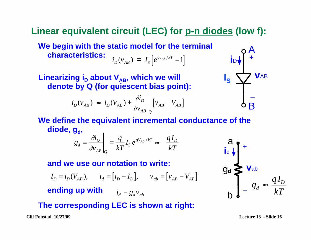
Linear equivalent circuit (LEC) for p-n diodes (low f): We begin with the static model for the terminal
characteristics:
Linearizing iD about VAB, which we will denote by Q (for quiescent bias point):
!
iD (vAB ) = IS eqvAB kT
"1[ ]
!
iD (vAB ) " iD (VAB ) +#iD
#vAB Q
vAB $VAB[ ] B
A
IBS
iD+
–
vABIS
We define the equivalent incremental conductance of the diode, g ,d
!
gd "#iD
#vAB Q
=q
kTIS e
qVAB / kT$
q ID
kT
and we use our notation to write: gd
b
a
vab
id+
–
!
gd "q ID
kT
!
ID = iD (VAB ), id = iD " ID[ ], vab = vAB "VAB[ ]
ending up with
The corresponding LEC is shown at right:
!
id = gdvab
Clif Fonstad, 10/27/09 Lecture 13 - Slide 16
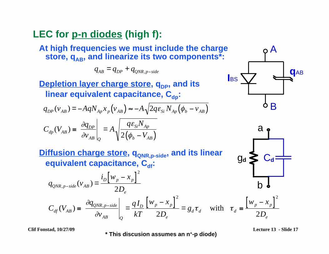
LEC for p-n diodes (high f): At high frequencies we must include the charge
store, qAB, and linearize its two components*:
gd Cd
b
a
B
A
IBS
qAB
!
qDP (vAB ) = "AqNAp xp vAB( ) # "A 2q$Si NAp %b " vAB( )
Cdp (VAB ) &'qDP
'vAB Q
= Aq$SiNAp
2 %b "VAB( )
!
qQNR ,p"side (vAB ) =iD wp " xp[ ]
2
2De
!
qAB = qDP + qQNR ,p"side
!
Cdf (VAB ) "#qQNR ,p$side
#vAB Q
=q ID
kT
wp $ xp[ ]2
2De
= gd% d with % d "wp $ xp[ ]
2
2De
Depletion layer charge store, qDP, and its linear equivalent capacitance, Cdp:
Diffusion charge store, qQNR,p-side, and its linear equivalent capacitance, Cdf:
Clif Fonstad, 10/27/09 Lecture 13 - Slide 17 * This discusion assumes an n+-p diode)
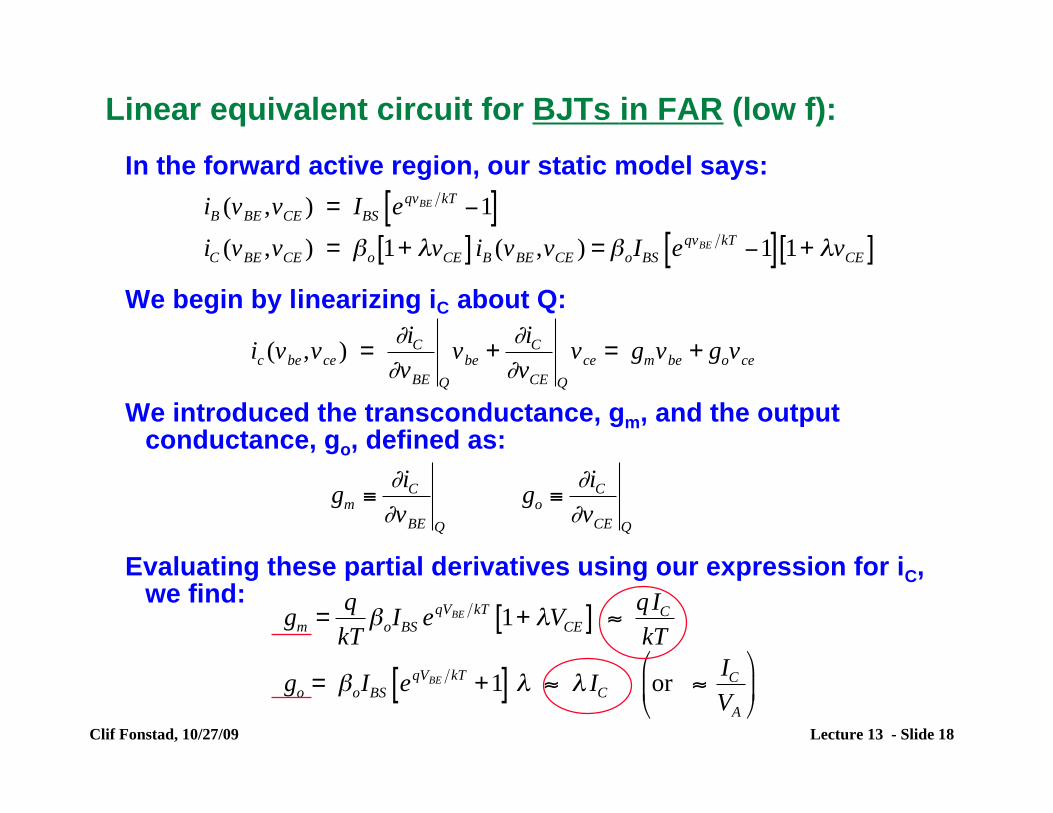
!
gm =q
kT"oIBS e
qVBE kT1+ #VCE[ ] $
q IC
kT
go = "oIBS eqVBE kT +1[ ] # $ # IC or $
IC
VA
%
& '
(
) *
Linear equivalent circuit for BJTs in FAR (low f): In the forward active region, our static model says:
!
iB (vBE ,vCE ) = IBS eqvBE kT "1[ ]
iC (vBE ,vCE ) = #o 1+ $vCE[ ] iB (vBE ,vCE ) = #oIBS eqvBE kT "1[ ] 1+ $vCE[ ]
We begin by linearizing i
!
ic (vbe,vce ) ="iC
"vBE Q
vbe +"iC
"vCE Q
vce = gmvbe + govce
C about Q:
We introduced the transconductance, gm, and the output conductance, go, defined as:
!
gm "#iC
#vBE Q
go "#iC
#vCE Q
Evaluating these partial derivatives using our expression for iC,we find:
Clif Fonstad, 10/27/09 Lecture 13 - Slide 18
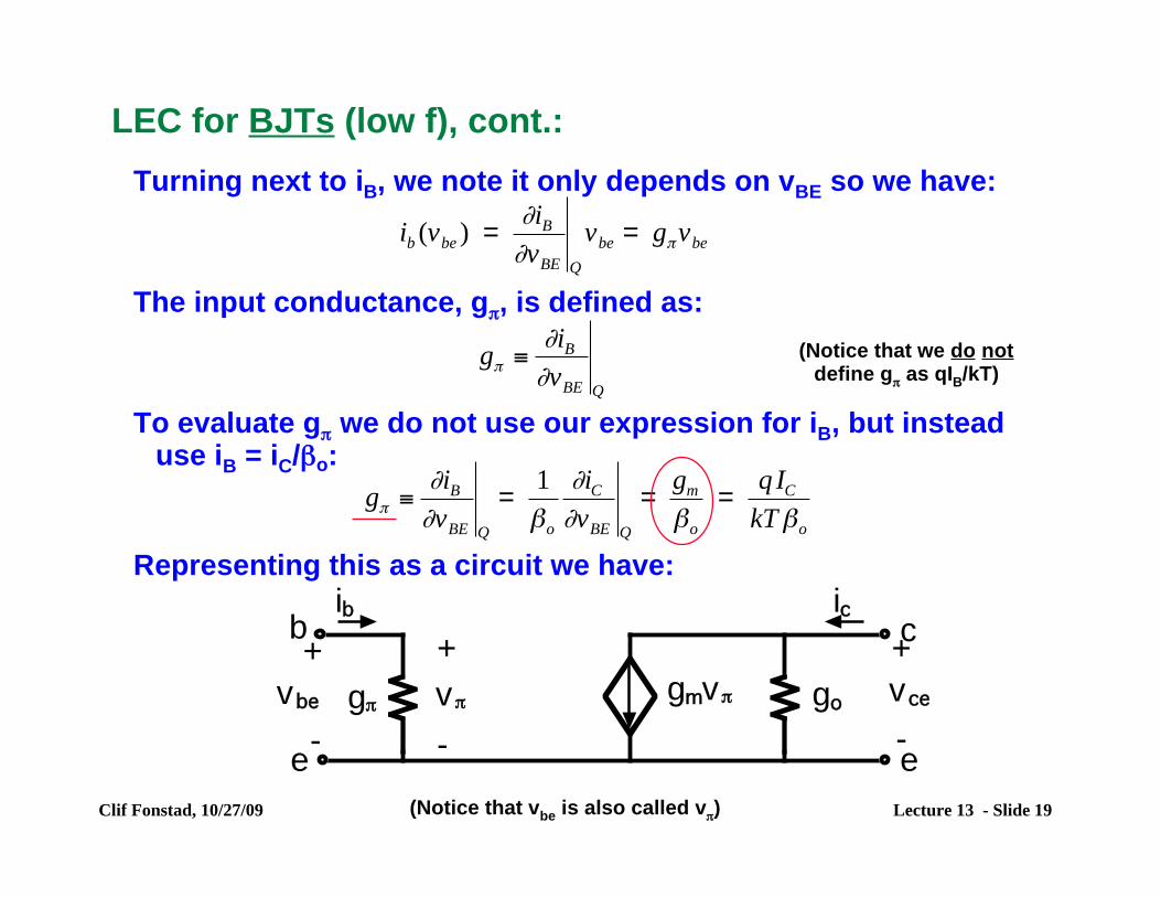
LEC for BJTs (low f), cont.: Turning next to iB, we note it only depends on vBE so we have:
!
ib (vbe ) ="iB
"vBE Q
vbe = g#vbe
The input conductance, gπ
!
g" #$iB
$vBE Q
, is defined as: (Notice that we do not
define gπ as qIB/kT)
To evaluate gπ we do not use our expression for iB, but instead use iB = iC/βo:
Representing this as a circuit we have:
!
g" #$iB
$vBE Q
=1
%o
$iC$vBE Q
=gm
%o
=q IC
kT%o
+
-
g! v!
b
e
gmv! go
e
cib
+
-
vbe
+
-
vce
ic
Clif Fonstad, 10/27/09 (Notice that vbe is also called vπ) Lecture 13 - Slide 19
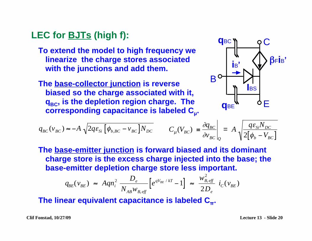
LEC for BJTs (high f): To extend the model to high frequency we
linearize the charge stores associated with the junctions and add them.
The base-collector junction is reverse biased so the charge associated with it, qBC, is the depletion region charge. The corresponding capacitance is labeled Cµ.
qBC
B
E
C
iB’
IBS
!FiB’
qBE
!
qBC (vBC ) " #A 2q$Si %b,BC # vBC[ ]NDC
!
Cµ (VBC) "#qBC
#vBC Q
= Aq$SiNDC
2 %b &VBC[ ]
The base-emitter junction is forward biased and its dominant charge store is the excess charge injected into the base; the base-emitter depletion charge store less important.
!
qBE(vBE ) " Aqni
2 De
NABwB, eff
eqVBE / kT
#1[ ] "wB, eff
2
2De
iC (vBE )
The linear equivalent capacitance is labeled Cπ.
Clif Fonstad, 10/27/09 Lecture 13 - Slide 20
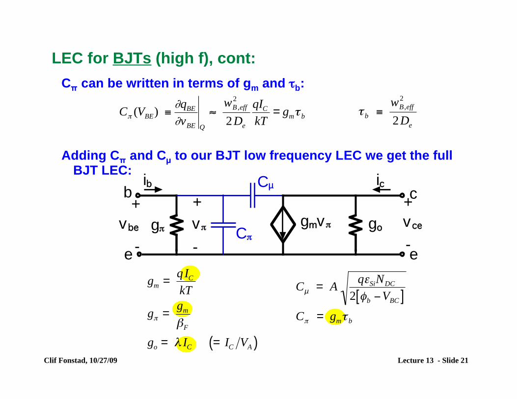
LEC for BJTs (high f), cont: Cπ can be written in terms of gm and τb:
!
C" (VBE) #$qBE
$vBE Q
%wB ,eff
2
2De
qIC
kT= gm& b
!
" b #wB ,eff
2
2De
Adding Cπ and Cµ to our BJT low frequency LEC we get the full BJT LEC:
!
gm =q IC
kT
g" =gm
#F
go = $ IC = IC VA( )
!
Cµ = Aq"SiNDC
2 #b $VBC[ ]C% = gm& b
+
-
g!C!
v!
b
e
Cµ
gmv! go
e
c+
-
vbe
ib
+
-
vce
ic
Clif Fonstad, 10/27/09 Lecture 13 - Slide 21

LEC for MOSFETs in saturation (low f): In saturation, our static model is: (Recall that α ≈ 1)
!
iG (vGS ,vDS ,vBS ) = 0 iB (vGS,vDS ,vBS ) " 0
iD (vGS ,vDS ,vBS ) =K
2#vGS $VT vBS( )[ ]2
1+ % vDS $VDS,sat( )[ ]
with K &W
LµeCox
* and VT = VTo + ' 2(p$Si $ vBS $ 2(p$Si( )
Note that because iG and iB are zero they are already linear, and we can focus on iD. Linearizing iD about Q we have:
!
id (vgs,vds,vbs) ="iD
"vGS Q
vgs +"iD
"vDS Q
vds +"iD
"vBS Q
vbs
= gmvgs + govds + gmbvbs
We have introduced the transconductance, gm, output conductance, go, and substrate transconductance, gmb:
!
gm "#iD
#vGS Q
go "#iD
#vDS Q
gmb "#iD
#vBS Q
Clif Fonstad, 10/27/09 Lecture 13 - Slide 22
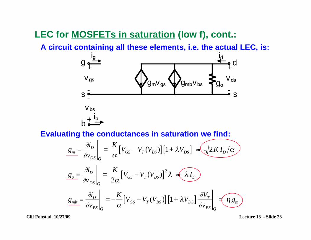
!
gm "#iD#vGS Q
=K
$VGS %VT (VBS )[ ] 1+ &VDS[ ] ' 2K ID $
go "#iD#vDS Q
=K
2$VGS %VT (VBS )[ ]2
& ' & ID
gmb "#iD#vBS Q
= %K
$VGS %VT (VBS )[ ] 1+ &VDS[ ] #VT
#vBS Q
= (gm
LEC for MOSFETs in saturation (low f), cont.: A circuit containing all these elements, i.e. the actual LEC, is:
Evaluating the conductances in saturation we find:
g
s
gmbvbs go
s
d
gmvgs
b
-
+
vbs
+
-
vgs
+
-
vds
ig id
ib
Clif Fonstad, 10/27/09 Lecture 13 - Slide 23

G
S
D qDB
iD
B
qSB
qG
straightforward compared to qG., as we will see below. qSB and qDB contribute two capacitors, Csb and Cdb, to our LEC.
LEC for MOSFETs in saturation (high f): For the high frequency model we
linearize and add the charge stores associated with each pair of terminals.
Two, qSB and qDB, are depletion region charge stores associated with the n+ regions of the sourceand drain. They are relatively
The gate charge, qG, depends in general on vGS, vDS, and vGB (= vGS-vBS), but in saturation, qG only depends on vGS and vGB (i.e. vGS and vBS) in our model, adding Cgs and Cgb.
When vGS ≥ VT the drain is ideally decoupled from the gate , but in any real device there is fringing capacitance between the gate electrode and the drain diffusion that we must include as Cgd, a parasitic element.
Clif Fonstad, 10/27/09 Lecture 13 - Slide 24
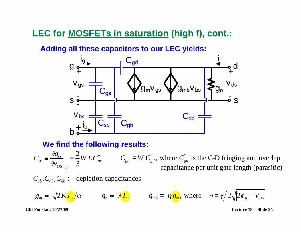
LEC for MOSFETs in saturation (high f), cont.:
We find the following results:
Adding all these capacitors to our LEC yields:
!
Cgs "#qG
#vGS Q
=2
3W LCox
*
!
Csb ,Cgb,Cdb : depletion capacitances
!
Cgd = W Cgd
*, where Cgd
* is the G-D fringing and overlap
!
capacitance per unit gate length (parasitic)
!
gm " 2K ID # go " $ ID gmb = %gm, where % = & 2 2'p (VBS
+
-Cgs
vgs
g
s
Cgd
gmbvbs go
s
d
gmvgs
b
-
+
vbs
Csb
CdbCgb
+
-
vds
ig id
ib
Clif Fonstad, 10/27/09 Lecture 13 - Slide 25

LEC for MOSFETs in saturation when vbs = 0: A very common situation in many circuits is that there is
no signal applied between on the base, i.e. vbs = 0 (even though it may be biased relative to the source, VBS ≠ 0).
In this case the MOSFET LEC simplifies significantly:
The elements that remain retain their original dependences:
!
Cdb : depletion capacitance
!
Cgs "#qG
#vGS Q
=2
3W LCox
*
!
Cgd = W Cgd
*, where Cgd
* is the G-D fringing and overlap
!
capacitance per unit gate length (parasitic)!
gm " 2K ID # go " $ ID
Cgs
Cgdg
s,b
go
s,b
d
gmvgs
-
+
-
vgs
+
-
vds
ig id
Cdb
Clif Fonstad, 10/27/09 Lecture 13 - Slide 26

LEC for Sub-threshold MOSFETs, vBS = 0: Our large signal model for MOSFETs operated in the sub-
threshold FAR (vDS >> kT/q) and vBS = 0, is:
G
S,B
D
iD(vGS, vDS)
iG (= 0)
iD
!
iD,s" t (vGS,vDS ) # IS,s" t 1" $vDS( )evGS "VTo{ } nVt
!
iG,s" t (vGS,vDS ,vBS ) = 0
Like a MOSFET in saturation with vbs = 0, the LEC has only
!
gm "#iD#vGS Q
=q
nkTIS,s$ t 1$ %VDS( )eq VGS $Vto( ) nkT =
q ID
nkT
go "#iD#vDS Q
= % IS,s$ t eq VGS $Vto( ) nkT & % ID or &
ID
VA
'
( )
*
+ ,
two elements, gm and go, but now gm is quite different:
Clif Fonstad, 10/27/09 Lecture 13 - Slide 27

LEC for Sub-threshold MOSFETs, vBS = 0, cont.:
!
gm =q ID
nkTgo " # ID
The LEC for MOSFETs in sub-threshold FAR (vDS >> kT/q) and vBS = 0, is:
g
s,b
go
s,b
d
gmvgs
-
+
-
vgs
+
-
vds
ig id
The charge store qDB is the same as qDB in a MOSFETs operated in strong inversion, but gG is not. gG is the gate capacitance in depletion (VFB < vGB < VT), so it is smaller in sub-threshold.
Clif Fonstad, 10/27/09 Lecture 13 - Slide 28
G
S,B
D qDB
iD
qG

LEC for Sub-threshold MOSFETs, vBS = 0, cont.: Adding the linear capacitors corresponding to the charge
stores we have:
* See Lecture 9, Slides 7 and 8, for qG and the derivation of Cgs.
Cgs
Cgdg
s,b
go
s,b
d
gmvgs
-
+
-
vgs
+
-
vds
ig id
Cdb
!
Cgs "#qG
#vGS Q
= W L Cox
$1+
2Cox
$2VGS %VFB( )&SiqNA
!
gm =q ID
nkTgo " # ID
!
Cdb : depletion capacitance
!
Cgd = W Cgd
*, where Cgd
* is the G-D fringing and overlap
Notice that as before, Cgd is zero in our ideal model. It a parasitic that cannot be avoided and must be included because it limits device and circuit performance.
Clif Fonstad, 10/27/09 Lecture 13 - Slide 29
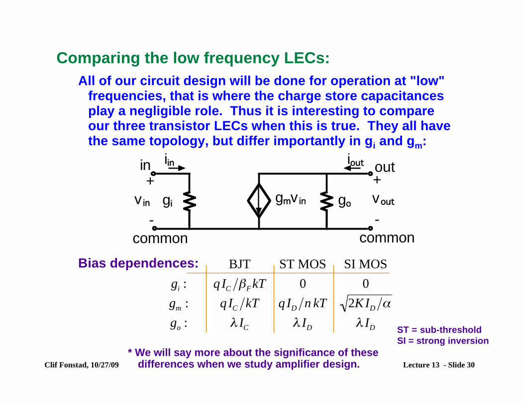
Comparing the low frequency LECs: All of our circuit design will be done for operation at "low"
frequencies, that is where the charge store capacitances play a negligible role. Thus it is interesting to compare our three transistor LECs when this is true. They all have the same topology, but differ importantly in gi and gm:
!
BJT ST MOS SI MOS
gi : q IC "FkT 0 0
gm : q IC kT q ID n kT 2KID #
go : $ IC $ ID $ ID
Bias dependences:
ST = sub-threshold
gi
in
common
gmv in go
common
outiin
+
-
v in
+
-
vout
iout
SI = strong inversion * We will say more about the significance of these
Clif Fonstad, 10/27/09 differences when we study amplifier design. Lecture 13 - Slide 30

The importance of the bias current: A very important observation is that all of the elements in
the three LECs we compared depend on the bias level of the output current, IC, in the case of a BJT, or ID, in the case of a MOSFET:
!
BJT ST MOS SI MOS
gi : q IC "FkT 0 0
gm : q IC kT q ID n kT 2KID #
go : $ IC $ ID $ ID
Bias dependences:
ST = sub-threshold SI = strong inversion
The bias circuitry is a key part of any linear amplifier. The designer must establish a stable bias point for all the transistors in the amplifier to insure that the gain remainsconstant and stable.
We will study amplifier design and practice beginning with Lecture 17.
Clif Fonstad, 10/27/09 Lecture 13 - Slide 31
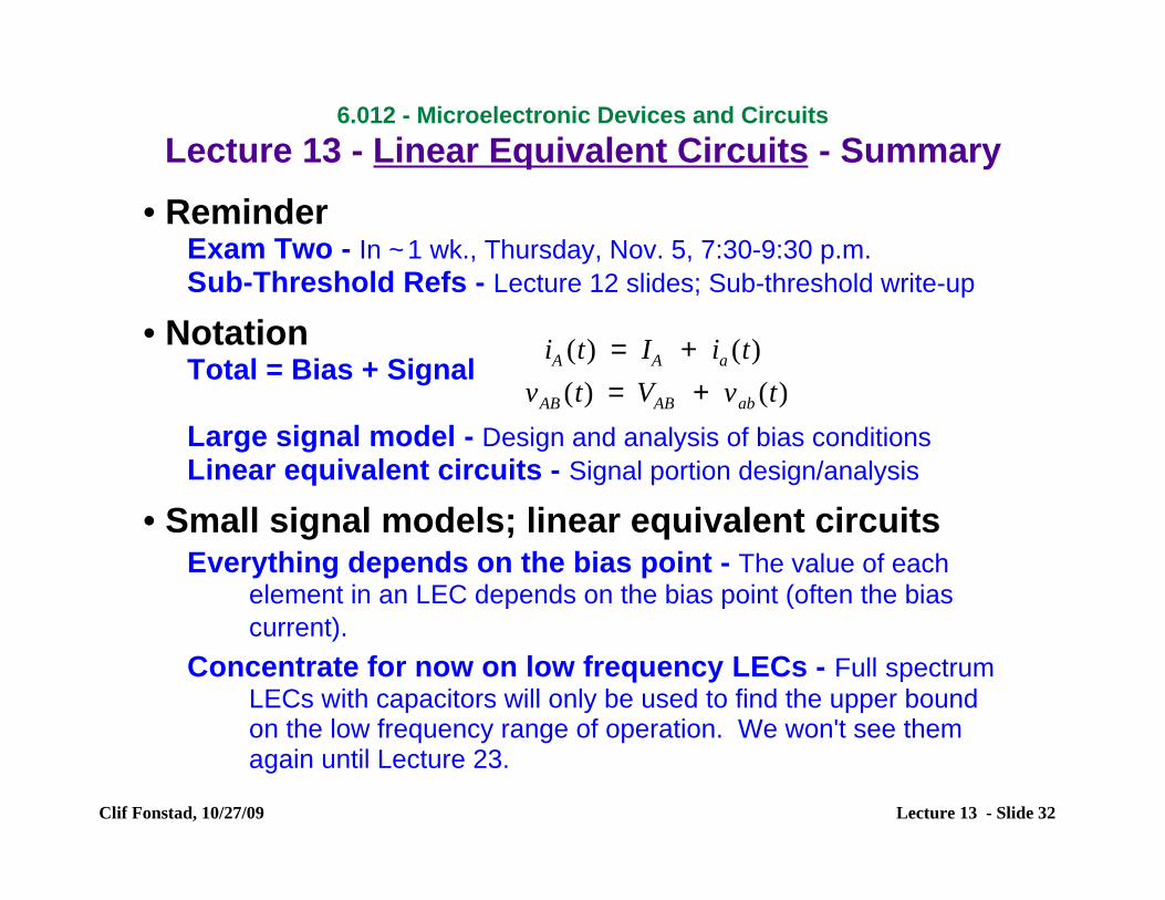
6.012 - Microelectronic Devices and Circuits Lecture 13 - Linear Equivalent Circuits - Summary
• Reminder Exam Two - In ~1 wk., Thursday, Nov. 5, 7:30-9:30 p.m. Sub-Threshold Refs - Lecture 12 slides; Sub-threshold write-up
• Notation Total = Bias + Signal
!
iA (t) = IA + ia (t)
vAB (t) = VAB + vab (t)
Large signal model - Design and analysis of bias conditions Linear equivalent circuits - Signal portion design/analysis
• Small signal models; linear equivalent circuits Everything depends on the bias point - The value of each
element in an LEC depends on the bias point (often the bias current).
Concentrate for now on low frequency LECs - Full spectrum LECs with capacitors will only be used to find the upper bound on the low frequency range of operation. We won't see them again until Lecture 23.
Clif Fonstad, 10/27/09 Lecture 13 - Slide 32

MIT OpenCourseWarehttp://ocw.mit.edu
6.012 Microelectronic Devices and Circuits Fall 2009
For information about citing these materials or our Terms of Use, visit: http://ocw.mit.edu/terms.