lkp with pfc - futureelectronics.com one/ak1601-7r.pdf · k series with pfc data sheet 150 – 280...
TRANSCRIPT

BCD20001-G Rev AC, 16-Dec-2010 Page 1 of 29 www.power-one.com
K Series with PFC Data Sheet150 – 280 Watt AC-DC Converters
Table of Contents Page Page
DescriptionThe LK 4000/5000 Series of AC-DC converters representsa flexible range of power supplies for use in advancedelectronic systems; the LKP models are an extension withincreased output power, but optimized to 230 VAC.Features include full power factor correction, good hold-uptime, high efficiency and reliability, low output noise, andexcellent dynamic response to load/line changes.The converters are protected against surges andtransients occurring at the source lines. Input over- andundervoltage lockout circuitry disables the outputs, whenthe input voltage is outside of the specified range. Inputinrush current limitation is included for preventing circuitbreakers and fuses from tripping at switch-on.All outputs are overload, open- and short-circuit proof, andprotected by a built-in suppressor diode. The outputs canbe inhibited by a logic signal applied to connector pin 18. Ifthe inhibit function is not used, pin 18 must be connectedwith pin 14 to enable the outputs.
LED indicators display the status of the converter andallow visual monitoring of the system at any time.Full input to output, input to case, output to case andoutput to output isolation is provided. The converters aredesigned and built according to the international safetystandards IEC/EN 60950-1 2nd Ed. They have beenapproved by the safety agencies TÜV and CSA (for USAand Canada).The case design allows operation at nominal load up to71 °C in a free air ambient temperature. If forced cooling isprovided, the ambient temperature may exceed 71 °C, butthe case temperature must remain below 95 °C under allconditions. However, higher output power up to 280 W ispossible depending on environmental conditions andconverter model.An internal temperature sensor generates an inhibit signal,which disables the outputs, when the case temperature TCexceeds the limit. The outputs automatically recover, when
1686.6"
803.2"16 TE
1114.4"3 U
Safety-approved to IEC/EN 60950-1 and UL/CSA60950-1 2nd Ed.
Description ...................................................................... 1Model Selection ............................................................... 2Functional Description .................................................... 4Electrical Input Data ........................................................ 5Electrical Output Data ..................................................... 8Auxiliary Functions ........................................................ 13
Electromagnetic Compatibility (EMC) .......................... 16Environmental Conditions ............................................ 17Mechanical Data ........................................................... 18Safety and Installation Instructions .............................. 20Description of Options .................................................. 22Accessories .................................................................. 28
Features• RoHS lead-free-solder and lead-solder-exempted
products are available.• Class I equipment• Power factor >0.93, harmonics IEC/EN 61000-3-2• Immunity according to IEC/EN 61000-4-2, -3, -4, -5, -6• High efficiency• Input over- and undervoltage lockout• Adjustable output voltage with remote on/off• 1 or 2 outputs: SELV, no load, overload, and short-
circuit proof• Rectangular current limiting characteristic• Immunity accord. to IEC 61000-4-2, -3, -4, -5, -6• PCBs protected by lacquer• Very high reliability

BCD20001-G Rev AC, 16-Dec-2010 Page 2 of 29 www.power-one.com
K Series with PFC Data Sheet150 – 280 Watt AC-DC Converters
Model SelectionNon-standard input/output configurations or special customer adaptations are available on request.
Table 1: Standard models
Output 1 Output 2 Operating input range Type designation Efficiency1 OptionsVo nom Io nom Vo nom Io nom Vi min – Vi max ηηηηη min[VDC] [A] [VDC] [A] [VAC] [%]
5.1 20 – – 85 – 264 LK4002-7R 79 E, P, D, V 2, P, T, K5, B, B1, B2 4, G5.1 25 – – LK4003-6R 79 E, P, D, V 2, P, T, K5, B, B1, B2 4, G
12 12 – – 85 – 264 LK4301-7R 84 -9E, P, D, T, B, B1, B2 4, G15 10 – – LK4501-7R 85 -9E, P, D, T, B, B1, B2 4, G24 6 – – LK4601-7R 86 -9E, P, D, T, B, B1, B2 4, G
12 6 12 3 6 85 – 264 LK5320-7R 82 -9E, P, D, T, B, B1, B2 4, G15 5 15 3 5 LK5540-7R 83 -9E, P, D, T, B, B1, B2 4, G24 3 24 3 3 LK5660-7R 83 -9E, P, D, T, B, B1, B2 4, G
12 10 12 3 10 187 – 255 LKP5320-6R 85 E, P, D, T, B, B1, B2 4, G24 5.2 24 3 5.2 LKP5660-7R 86 -9E, P, D, T, B, B1, B2 4, G24 5.8 24 3 5.8 LKP5661-5R 86 E, P, D, T, B, B1, B2 4, G
1 Min. efficiency at Vi nom, I o nom and TA = 25 °C. Typical values are approximately 2% better.2 Option V for models with 5.1 V outputs; excludes option D3 Second output semi-regulated4 For customer-specific models with 220 mm case length5 For new designs, use only option K.
Table 2: Battery charger models
Nom. output values Output range 5 Operating input range Type designation Efficiency1 OptionsVo nom Io nom Vo min – Vo max Vi min – Vi max ηηηηη min[VDC] [A] [VDC] [VAC] [%]
12.84 10 12.62 – 14.12 85 – 264 LK4740-7R 84 -9E, D, T, B, B1, B2 4, G25.68 2 5.4 25.25 – 28.25 LK5740-7R 83 -9E, D, T, B, B1, B2 4, G51.36 3 2.7 25.5 – 56.5 LK5740-7R 83 -9E, D, T, B, B1, B2 4, G
25.68 2 9 25.25 – 28.25 187 – 255 LKP5740-7R 86 -9E, D, T, B, B1, B2 4, G25.68 2 10 25.25 – 28.25 LKP5741-5R 86 E, D, T, B, B1, B2 4, G
51.36 3 4.5 50.5 – 56.5 187 – 255 LKP5740-7R 86 -9E, D, T, B, B1, B2 4, G51.36 3 5 50.5 – 56.5 LKP5741-5R 85 E, D, T, B, B1, B2 4, G
1 Min. efficiency at Vi nom, Io nom and TA = 25 °C. Typical values are approximately 2% better.2 Both outputs connected in parallel3 Both outputs connected in series4 For customer-specific models with 220 mm case length5 Controlled by the battery temperature sensor, see Accessories
the temperature drops below the limit.Various options are available to adapt the converters toindividual applications. An external temperature sensor isavailable to allow for temperature adapted batterycharging.The converters may either be plugged into 19" rack
systems according to IEC 60297-3, or be mounted on achassis or plate.
Important:These products are intended to replace the LK1000 andLK2000 models, in order to comply with IEC/EN 61000-3-2.For applications with DC input or main frequencies other than50/60 Hz, the LK1000 and LK2000 models are still available.

BCD20001-G Rev AC, 16-Dec-2010 Page 3 of 29 www.power-one.com
K Series with PFC Data Sheet150 – 280 Watt AC-DC Converters
Example: LK5540-9EPD3TB1: Power factor corrected AC-DC converter, operating input voltage range 85 – 264 VAC,2 electrically isolated outputs, each providing 15 V, 5 A, equipped with inrush current limiter, a potentiometer toadjust the output voltages, undervoltage monitor D3, current share feature, and a cooling plate B1.
Product MarkingBasic type designation, applicable approval marks, CEmark, warnings, pin designation, Power-One patents andcompany logo, identification of LEDs, test sockets, andpotentiometer.Specific type designation, input voltage range, nominaloutput voltages and currents, degree of protection, batchno., serial no., and data code including production site,modification status, and date of production.
Part Number DescriptionOperating input voltage Vi:
85 – 264 VAC ............................................................ LK187 – 255 VAC ........................................................LKP
Number of outputs (4 = single, 5 = double) ................... 4, 5Single-output models:Nominal voltage output 1 (main output), Vo1 nom
5.1 V ..................................................................... 0, 1, 212 V ............................................................................. 315 V ......................................................................... 4, 524 V ............................................................................. 6Other voltages 1 ....................................................... 7, 8Other specifications (single-output models)1 .... 21 – 9 9
Double-output models:Nominal voltage output 1 and 2
12 V, 12 V ............................................................................................... 2015 V, 15 V ............................................................................................... 4024 V, 24 V ................................................................... 60Other specifications or additional features 1 ..... 70 – 99
Operational ambient temperature range TA:–25 to 71 °C ............................................................... -7–40 to 71 °C ................................................................ -9–25 2 to 60 °C .............................................................. -6–25 2 to 50 °C .............................................................. -5Other 1 ......................................................................... -0
Auxiliary functions and options:Inrush current limitation ............................................. E 2
Output voltage control input ....................................... R 3
Potentiometer (output voltage adjustment) ................ P 3
Undervoltage monitor (D0 – DD, to be specified) ...... D 4
ACFAIL signal (V2, V3, to be specified) .................... V 4
Current share .............................................................. TH15S4 connector (rather then H15S2) ..................... K 5
Cooling plate standard case ............................ B or B1Cooling plate for long case 220 mm 1 ...................... B2RoHS-compliant for all 6 substances ...................... G6
1 Customer-specific models2 Option E is mandatory for all -9 models. Models with -5E or -6E are functional down to –40 °C.3 Feature R excludes option P and vice versa. Option P is not available for battery charger models.4 Option D excludes option V and vice versa; option V is available for models with 5.1 V output only (LK4003, etc.).5 Option K is available for models with 5.1 V output only (LK4002, LK4003, etc.) to ensure compatibility with LK1001 models.6 G is always placed at the end of the part number.
LK 5 5 40 -9 E P D3 T K B1

BCD20001-G Rev AC, 16-Dec-2010 Page 4 of 29 www.power-one.com
K Series with PFC Data Sheet150 – 280 Watt AC-DC Converters
Fig. 2Block diagram of double-output models
1 Transient suppressor (VDR)2 Inrush current limiter (NTC, only models with TA min = –25 °C ) or option E3 Bulk capacitor Cb; bulk voltage approx. 370 V
Functional DescriptionThe input voltage is fed via an input fuse, an input filter, arectifier, and an inrush current limiter to a boost converter.This step-up converter provides a sinusoidal input current(IEC/EN 61000-3-2, class D equipment) and charges thebulk capacitor Cb to approx. 370 VDC. This capacitorsources a single-transistor forward converter and providesthe power during the hold-up time.The main transformer exhibits a separate secondarywinding for each output. Each generated voltage isrectified and smoothed by the power choke and the output
filter. The control logic senses the main output voltage Voor Vo1 and generates, with respect to the maximumadmissible output currents, the control signal for theswitching transistor of the forward converter.The second output of double output models is tracking tothe main output, but has its own current limiting circuit. Ifthe main output voltage drops due to current limitation, thesecond output voltage will fall as well and vice versa.A separate auxiliary converter generates the supplyvoltages for all primary and secondary control circuits andoptions.
Fig. 1Block diagram of single-output models
1 Transient suppressor (VDR)2 Inrush current limiter (NTC, only models with TA min = –25 °C ) or option E3 Bulk capacitor Cb; bulk voltage approx. 370 V
Co
ntr
ol circu
it
P
16
18
20
22
12
14
4
6
8
10
Ou
tpu
t 2
filte
r
Ou
tpu
t 1
filte
r
26
28
3032
24
– +
03002c
N~
L~
R
i
D
T
Vo1+
Vo1–
Vo2+
Vo2–
CY
Inp
ut
filte
r
1
Brid
ge
re
tifie
r
CY
CY
Fu
se
Fo
rwa
rd c
on
ve
rte
r (a
pp
rox.
80
kH
z)
+
Bo
ost
co
nve
rte
r (a
pp
rox.
10
0 k
Hz)
Ci 3
2
Input filter
Contr
ol circuit
P
2
16
18
20
22
12
4
6
8
10
14
Outp
ut
filter
28
3032
24
– +
Forw
ard
convert
er
(appro
x. 80 k
Hz)
+
Boost convert
er
(appro
x. 100 k
Hz)
Ci 3
03001c
R
i
D/V
T
S+
Vo+
Vo–
S–
26N~
L~
1
Bridge r
etifier
Fuse
CY
CY
CY
CY
BCD20001-G Rev AC, 16-Dec-2010 Page 5 of 29 www.power-one.com
K Series with PFC Data Sheet150 – 280 Watt AC-DC Converters
Electrical Input DataGeneral Conditions:
– TA = 25 °C, unless TC is specified.– Pin 18 connected to pin 14, R input not connected, Vo adjusted to Vo nom (option P)– Sense line pins S+ and S– connected to Vo+ and Vo–, respectively (single-output models)
Table 3: Electrical input data
Input LK LKP Unit
Characteristics Conditions min typ max min typ max
Vi Rated input voltage range Io = 0 – Io nom 100 240 200 240 VAC 1
Vi op Operating input voltage range TC min to TC max 85 264 187 255
Vi nom Nominal input voltage 50 – 60 Hz 230 230
Ii Input current Vi nom, Io nom 2 0.8 1.25 A
P i0 No-load input power V i min – Vi max, Io = 0 9 10 9 10 W
P i inh Idle input power converter inhibited 3.5 5 3.5 5
R i Input resistance 480 480 mΩ
RNTC NTC resistance (see fig. 3)3 conv. not operating 3200 4000 3200 4000Cb Input capacitance 100 150 180 110 136 165 µF
Vi RFI Conducted input RFI EN 55011/55022 B B
Radiated input RFI Vi nom, Io nom A B
Vi abs Input voltage limits 283 283 VACwithout damage –400 400 –400 400 VDC 4
1 Rated input frequency: 50 – 60 Hz, operating frequency: 47 – 63 Hz. For operation at other frequencies, contact Power-One.2 With double-output models, both outputs loaded with Io nom3 Valid for models without option E. This is the value of the NTC resistance at 25 °C and applies to cold converters for the initial
switch-on cycle. Subsequent switch-on/off cycles increase the inrush current peak value.4 Operation with DC input voltage is not specified and not recommended.
Input Fuse and ProtectionA VDR together with the input fuse and a symmetrical inputfilter form an effective protection against high inputtransient voltages.A fuse mounted inside the converter in series to the phaseline protects against severe defects. A second fuse in theneutral line may be necessary in certain applications; seeInstallation Instructions.
Table 4: Fuse specification
Model Fuse type Fuse rating
LK4/5000 slow-blow SP T, 4 A, 250 V, 5 × 20 mm
LKP slow-blow SP T, 4 A, 250 V, 5 × 20 mm
Input Under- /Overvoltage LockoutIf the input voltage remains below approx. 65 VAC (LKP:150 VAC) or exceeds Vi abs, an internally generated inhibitsignal disables the output(s). Do not check the overvoltagelockout function!If Vi is below Vi min, but above the undervoltage lockoutlevel, the output voltage may be below the value specifiedin the tables Electrical Output Data.
Inrush Current LimitationThe models without option E incorporate an NTC resistorin the input circuitry, which at initial turn-on reduces thepeak inrush current value by a factor of 5 to 10 to protectconnectors and switching devices against damage.Subsequent switch-on cycles within short periods willcause an increase of the peak inrush current value due tothe warming-up of the NTC resistor.The inrush current peak value (initial switch-on cycle) canbe determined by following calculation:
Vi • √ 2––
Iinr p = –––––––––––––––– (Rs ext + R i + RNTC)
Fig. 3Equivalent circuit diagram for input impedance.
Rs ext Ri RNTCIinr p
Vi Cb
04001b
∼ +
BCD20001-G Rev AC, 16-Dec-2010 Page 6 of 29 www.power-one.com
K Series with PFC Data Sheet150 – 280 Watt AC-DC Converters
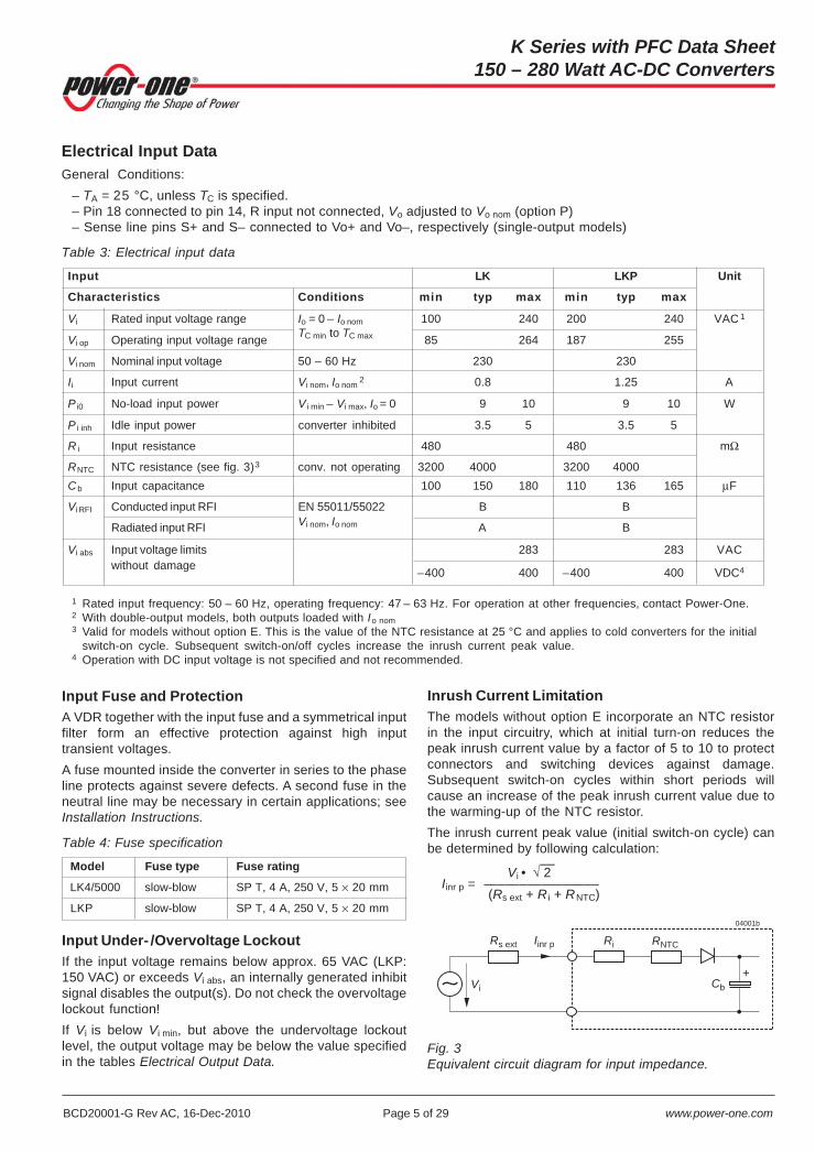
Fig. 4Theoretical worst case input inrush current versustime at Vi = 255 V, Rext = 0 for models withoutoption E
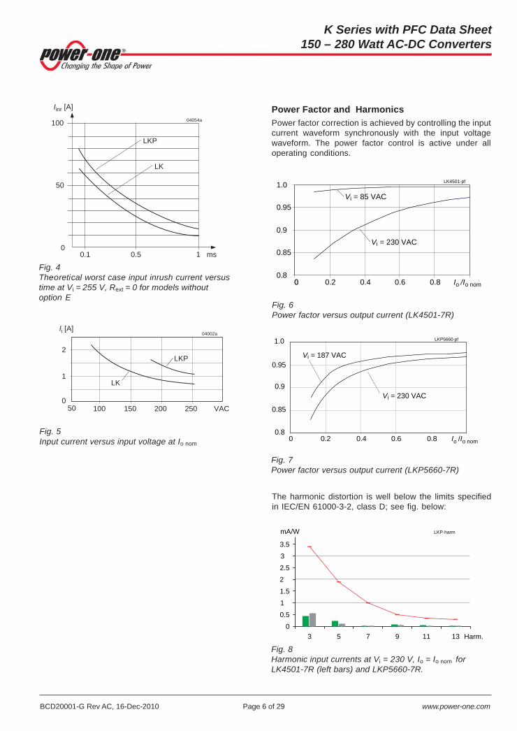
Fig. 5Input current versus input voltage at Io nom
Power Factor and HarmonicsPower factor correction is achieved by controlling the inputcurrent waveform synchronously with the input voltagewaveform. The power factor control is active under alloperating conditions.
Fig. 6Power factor versus output current (LK4501-7R)
0.1 1 ms
50
100
Iinr [A]
0
LKP
04054a
0.5
LK
The harmonic distortion is well below the limits specifiedin IEC/EN 61000-3-2, class D; see fig. below:
Fig. 8Harmonic input currents at Vi = 230 V, Io = Io nom forLK4501-7R (left bars) and LKP5660-7R.
Fig. 7Power factor versus output current (LKP5660-7R)
0
0.5
1
1.5
2
2.5
3
3.5
4
3 5 7 9 11 13
LKP-harmmA/W
Harm.
0.8
0.85
0.9
0.95
1.0
0 0 0.2 0.4 0.6 0.8 Io /Io nom
Vi = 85 VAC
Vi = 230 VAC
LK4501-pf
0.8
0.85
0.9
0.95
1.0
0 0.2 0.4 0.6 0.8 Io /Io nom
Vi = 230 VAC
Vi = 187 VAC
LKP5660-pf
100 150 200 250 VAC500
1
2
li [A]04002a
LKP
LK
BCD20001-G Rev AC, 16-Dec-2010 Page 7 of 29 www.power-one.com
K Series with PFC Data Sheet150 – 280 Watt AC-DC Converters
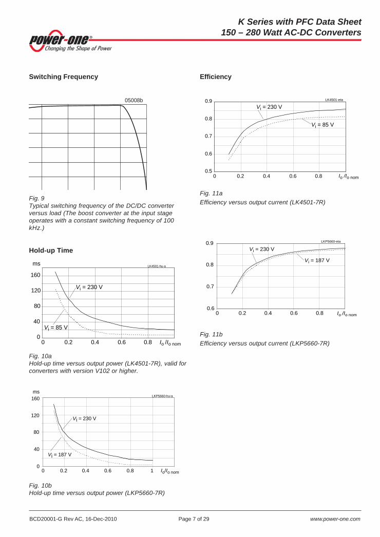
Fig. 10aHold-up time versus output power (LK4501-7R), valid forconverters with version V102 or higher.
Fig. 10bHold-up time versus output power (LKP5660-7R)
Efficiency
Fig. 11bEfficiency versus output current (LKP5660-7R)
Fig. 11aEfficiency versus output current (LK4501-7R)
05008b
Fig. 9Typical switching frequency of the DC/DC converterversus load (The boost converter at the input stageoperates with a constant switching frequency of 100kHz.)
Hold-up Time
Switching Frequency
0
40
80
120
160
0 0.2 0.4 0.6 0.8 1 Io/Io nom
LKP5660-hu-a
Vi = 230 V
Vi = 187 V
ms
0
40
80
120
160
ms
0 0.2 0.4 0.6 0.8 Io /Io nom
Vi = 230 V
Vi = 85 V
LK4501-hu-a
0.5
0.6
0.7
0.8
0.9
0 0.2 0.4 0.6 0.8 Io /Io nom
LK4501-eta
Vi = 230 V
Vi = 85 V
0.6
0.7
0.8
0 0.2 0.4 0.6 0.8 Io /Io nom
Vi = 187 V
Vi = 230 V0.9 LKP5660-eta
BCD20001-G Rev AC, 16-Dec-2010 Page 8 of 29 www.power-one.com
K Series with PFC Data Sheet150 – 280 Watt AC-DC Converters
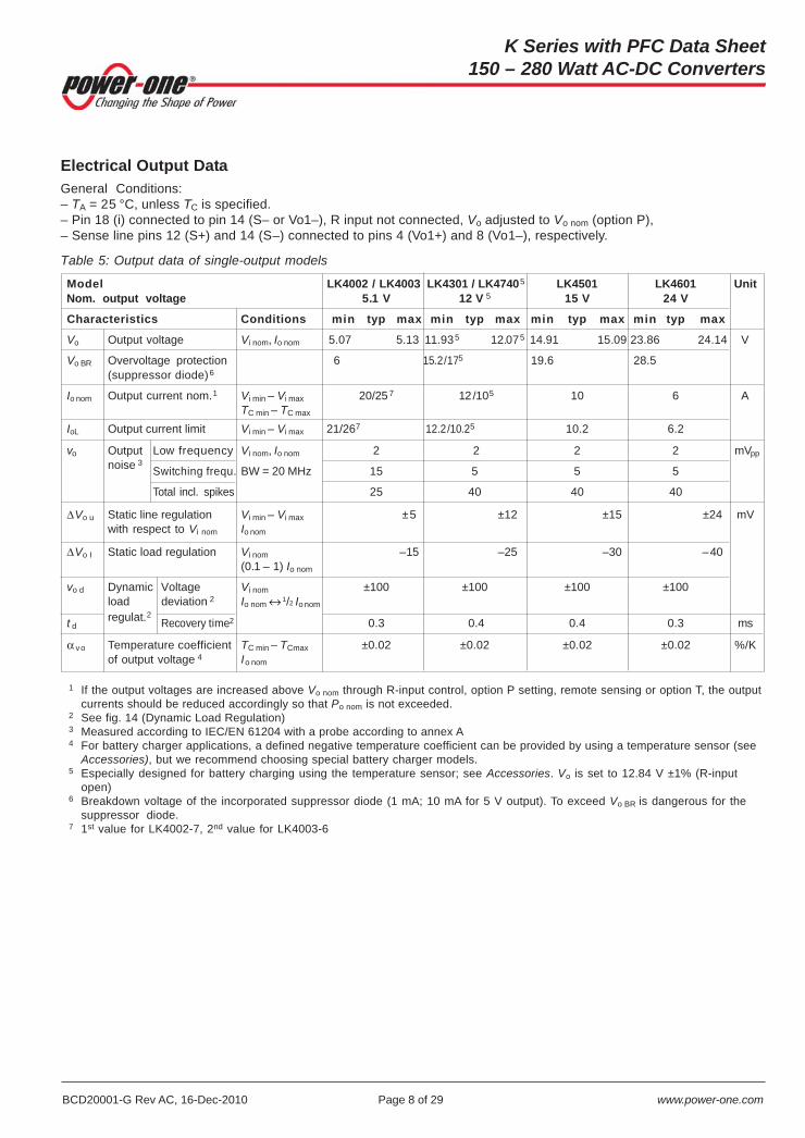
Electrical Output DataGeneral Conditions:– TA = 25 °C, unless TC is specified.– Pin 18 (i) connected to pin 14 (S– or Vo1–), R input not connected, Vo adjusted to Vo nom (option P),– Sense line pins 12 (S+) and 14 (S–) connected to pins 4 (Vo1+) and 8 (Vo1–), respectively.
Table 5: Output data of single-output models
Model LK4002 / LK4003 LK4301 / LK47405 LK4501 LK4601 UnitNom. output voltage 5.1 V 12 V 5 15 V 24 V
Characteristics Conditions min typ max min typ max min typ max min typ max
Vo Output voltage Vi nom, Io nom 5.07 5.13 11.935 12.075 14.91 15.09 23.86 24.14 V
Vo BR Overvoltage protection 6 15.2/175 19.6 28.5(suppressor diode)6
Io nom Output current nom. 1 Vi min – Vi max 20/25 7 12 / 105 10 6 ATC min – TC max
IoL Output current limit Vi min – Vi max 21/267 12.2/10.25 10.2 6.2
vo Output Low frequency Vi nom, Io nom 2 2 2 2 mVppnoise 3
Switching frequ. BW = 20 MHz 15 5 5 5
Total incl. spikes 25 40 40 40
∆Vo u Static line regulation Vi min – Vi max ±5 ±12 ±15 ±24 mVwith respect to Vi nom Io nom
∆Vo I Static load regulation Vi nom –15 –25 –30 –40(0.1 – 1) Io nom
vo d Dynamic Voltage Vi nom ±100 ±100 ±100 ±100load deviation 2 Io nom ↔ 1/2 Io nom
t dregulat. 2 Recovery time2 0.3 0.4 0.4 0.3 ms
α vo Temperature coefficient TC min – TCmax ±0.02 ±0.02 ±0.02 ±0.02 %/Kof output voltage 4 Io nom
1 If the output voltages are increased above Vo nom through R-input control, option P setting, remote sensing or option T, the outputcurrents should be reduced accordingly so that Po nom is not exceeded.
2 See fig. 14 (Dynamic Load Regulation)3 Measured according to IEC/EN 61204 with a probe according to annex A4 For battery charger applications, a defined negative temperature coefficient can be provided by using a temperature sensor (see
Accessories), but we recommend choosing special battery charger models.5 Especially designed for battery charging using the temperature sensor; see Accessories. Vo is set to 12.84 V ±1% (R-input
open)6 Breakdown voltage of the incorporated suppressor diode (1 mA; 10 mA for 5 V output). To exceed Vo BR is dangerous for the
suppressor diode.7 1st value for LK4002-7, 2nd value for LK4003-6

BCD20001-G Rev AC, 16-Dec-2010 Page 9 of 29 www.power-one.com
K Series with PFC Data Sheet150 – 280 Watt AC-DC Converters
1 Same conditions for both outputs2 If the output voltages are
increased above Vo nom via R-input control, option P setting,remote sensing or option T, theoutput currents should bereduced accordingly so thatPo nom is not exceeded.
3 Measured according to IEC/EN61204 with a probe annex A
4 See Dynamic Load Regulation5 See Output Voltage Regulation
of Double-Output Models6 For battery charger applications
a defined negative temperaturecoefficient can be provided byusing a temperature sensor;see Accessories.
7 Especially designed for batterycharging using the batterytemperature sensor; seeAccessories.Vo1 is set to 25.68 V ±1% (R-input open).
8 Breakdown voltage of theincorporated suppressordiodes (1 mA). ExceedingVo BR is dangerous for thesuppressor diodes.
Model LK5660 / 5740 7 UnitNom. output voltage 2 ××××× 24 V / 25.68 V7
Characteristics Conditions Output 1 Output 2
min typ max min typ max
Vo Output voltage Vi nom, Io nom 1 23.86 7 24.14 7 23.64 7 24.36 7 V
Vo BR Overvoltage protection 28.5/347 28.5/347
(suppressor diode) 8
Io nom Output current nom. 2 Vi min – Vi max 3 / 2.77 3 / 2.7 7 ATC min – TC max
IoL Output current limit Vi min – Vi max 3.2 3.2
vo Output Low frequency Vi nom, Io nom 3 3 mVppnoise 3
Switching freq. BW = 20 MHz 10 10Total incl. spikes 80 60
∆Vo u Static line regulation Vi min – Vi max ±20 5 mVwith respect to Vi nom 3 Io nom
∆Vo I Static load regulation 1 Vi nom –40 5
(0.1 – 1) Io nom
vo d Dynamic Voltage Vi nom ±100 ±150load deviation 4 Io1 nom ↔ 1/2 Io1 nom
t dregulat.3 Recovery time4 1/2 Io2 nom 0.3 ms
α vo Temperature coefficient TC min – TC max ±0.02 %/Kof output voltage 6 Io nom
Table 6a: Output data of double-output LK models. General conditions as in table 5.
Model LK5320 LK5540 UnitNom. output voltage 2 ××××× 12 V 2 ××××× 15 V
Characteristics Conditions Output 1 Output 2 Output 1 Output 2
min typ max min typ max min typ max min typ max
Vo Output voltage Vi nom, Io nom 1 11.93 12.07 11.82 12.18 14.91 15.09 14.78 15.22 V
Vo BR Overvoltage protection 15.2 15.2 19.6 19.6(suppressor diode) 8
Io nom Output current nom.2 Vi min – Vi max 6 6 5 5 ATC min – TC max
IoL Output current limit Vi min – Vi max 6.2 6.2 5.2 5.2vo Output Low frequency Vi nom, Io nom 3 3 3 3 mVpp
noise 3Switching freq. BW = 20 MHz 12 12 10 10
Total incl. spikes 70 60 80 60
∆Vo u Static line regulation Vi min – Vi max ±12 5 ±15 5 mVwith respect to Vi nom Io nom
∆Vo I Static load regulation1 Vi nom –40 5 –50 5
(0.1 – 1) Io nom
vo d Dynamic Voltage Vi nom, ±100 ±150 ±100 ±150load deviation 4 Io1 nom ↔ 1/2 Io1 nom
t dregulat.3 Recovery time4 1/2 Io2 nom 0.3 0.4 ms
α vo Temperature coefficient TC min – TC max ±0.02 ±0.02 %/Kof output voltage 6 Io nom
Table 6b: Output data of double-output LK models. General conditions as in table 5.
BCD20001-G Rev AC, 16-Dec-2010 Page 10 of 29 www.power-one.com
K Series with PFC Data Sheet150 – 280 Watt AC-DC Converters
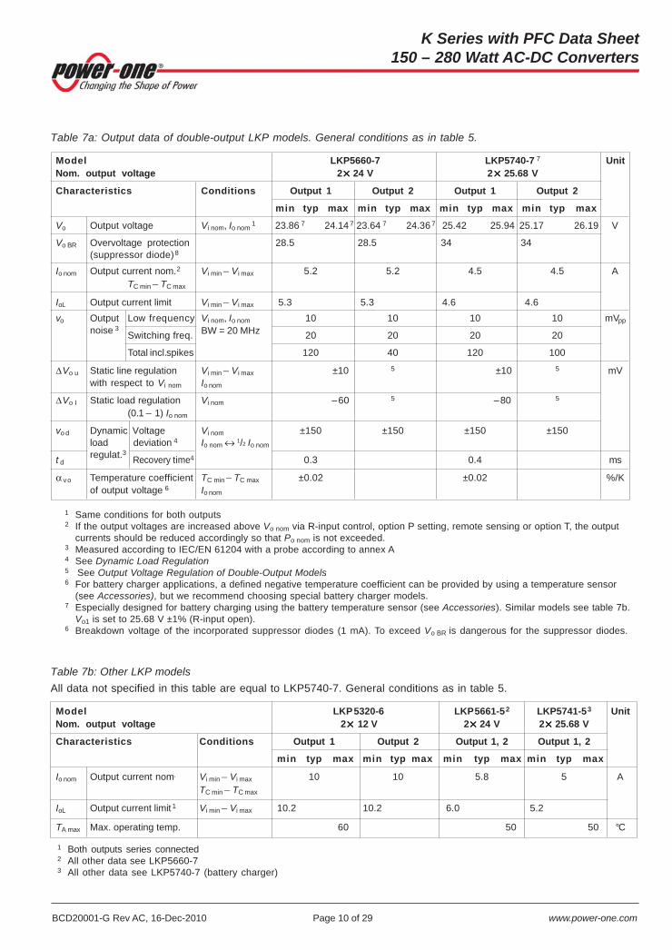
Table 7a: Output data of double-output LKP models. General conditions as in table 5.
Model LKP5660-7 LKP5740-7 7 UnitNom. output voltage 2 ××××× 24 V 2 ××××× 25.68 V
Characteristics Conditions Output 1 Output 2 Output 1 Output 2
min typ max min typ max min typ max min typ max
Vo Output voltage Vi nom, Io nom 1 23.86 7 24.14 7 23.64 7 24.36 7 25.42 25.94 25.17 26.19 V
Vo BR Overvoltage protection 28.5 28.5 34 34 (suppressor diode)8
Io nom Output current nom. 2 Vi min – Vi max 5.2 5.2 4.5 4.5 ATC min – TC max
IoL Output current limit Vi min – Vi max 5.3 5.3 4.6 4.6vo Output Low frequency Vi nom, Io nom 10 10 10 10 mVpp
noise 3Switching freq. BW = 20 MHz 20 20 20 20
Total incl. spikes 120 40 120 100
∆Vo u Static line regulation Vi min – Vi max ±10 5 ±10 5 mVwith respect to Vi nom Io nom
∆Vo I Static load regulation Vi nom –60 5 –80 5
(0.1 – 1) Io nom
vo d Dynamic Voltage Vi nom ±150 ±150 ±150 ±150load deviation 4 Io nom ↔ 1/2 Io nom
t dregulat.3 Recovery time4 0.3 0.4 ms
α vo Temperature coefficient TC min – TC max ±0.02 ±0.02 %/Kof output voltage 6 Io nom
1 Same conditions for both outputs2 If the output voltages are increased above Vo nom via R-input control, option P setting, remote sensing or option T, the output
currents should be reduced accordingly so that Po nom is not exceeded.3 Measured according to IEC/EN 61204 with a probe according to annex A4 See Dynamic Load Regulation5 See Output Voltage Regulation of Double-Output Models6 For battery charger applications, a defined negative temperature coefficient can be provided by using a temperature sensor
(see Accessories), but we recommend choosing special battery charger models.7 Especially designed for battery charging using the battery temperature sensor (see Accessories). Similar models see table 7b.
Vo1 is set to 25.68 V ±1% (R-input open).6 Breakdown voltage of the incorporated suppressor diodes (1 mA). To exceed Vo BR is dangerous for the suppressor diodes.
Table 7b: Other LKP modelsAll data not specified in this table are equal to LKP5740-7. General conditions as in table 5.
Model LKP5320-6 LKP5661-52 LKP5741-53 UnitNom. output voltage 2 ××××× 12 V 2××××× 24 V 2××××× 25.68 V
Characteristics Conditions Output 1 Output 2 Output 1, 2 Output 1, 2
min typ max min typ max min typ max min typ max
Io nom Output current nom. Vi min – Vi max 10 10 5.8 5 ATC min – TC max
IoL Output current limit 1 Vi min – Vi max 10.2 10.2 6.0 5.2
TA max Max. operating temp. 60 50 50 °C
1 Both outputs series connected2 All other data see LKP5660-73 All other data see LKP5740-7 (battery charger)
BCD20001-G Rev AC, 16-Dec-2010 Page 11 of 29 www.power-one.com
K Series with PFC Data Sheet150 – 280 Watt AC-DC Converters
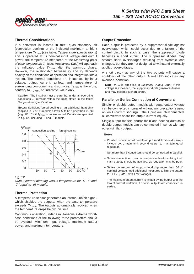
Thermal ConsiderationsIf a converter is located in free, quasi-stationary air(convection cooling) at the indicated maximum ambienttemperature TA max (see table: Temperature specifications)and is operated at its nominal input voltage and outputpower, the temperature measured at the Measuring pointof case temperature TC (see: Mechanical Data) will approachthe indicated value TC max after the warm-up phase.However, the relationship between TA and TC dependsheavily on the conditions of operation and integration into asystem. The thermal conditions are influenced by inputvoltage, output current, airflow, and temperature ofsurrounding components and surfaces. TA max is therefore,contrary to TC max, an indicative value only.
Caution: The installer must ensure that under all operatingconditions TC remains within the limits stated in the table:Temperature specifications.
Notes: Sufficient forced cooling or an additional heat sink(applied to -7 or -9) models allows TA to be higher than 71 °C(e.g., 85 °C), if TC max is not exceeded. Details are specifiedin fig. 12, including -5 and -6 models.
Fig. 12Output current derating versus temperature for -5, -6, and-7 (equal to -9) models.
Thermal ProtectionA temperature sensor generates an internal inhibit signal,which disables the outputs, when the case temperatureexceeds TC max. The outputs automatically recover, whenthe temperature drops below this limit.Continuous operation under simultaneous extreme worst-case conditions of the following three parameters shouldbe avoided: Minimum input voltage, maximum outputpower, and maximum temperature.
Output ProtectionEach output is protected by a suppressor diode againstovervoltage, which could occur due to a failure of thecontrol circuit. In such a case, the suppressor diodebecomes a short circuit. The suppressor diodes maysmooth short overvoltages resulting from dynamic loadchanges, but they are not designed to withstand externallyapplied overvoltages.A short circuit at any of the two outputs will cause ashutdown of the other output. A red LED indicates anyoverload condition.
Note: Vo BR is specified in Electrical Output Data. If thisvoltage is exceeded, the suppressor diode generates lossesand may become a short circuit.
Parallel or Series Connection of ConvertersSingle- or double-output models with equal output voltagecan be connected in parallel without any precautions usingoption T (current sharing). If the T pins are interconnected,all converters share the output current equally.Single-output models and/or main and second outputs ofdouble-output models can be connected in series with anyother (similar) output.
Notes:
– Parallel connection of double-output models should alwaysinclude both, main and second output to maintain goodregulation.
– Not more than 5 converters should be connected in parallel.
– Series connection of second outputs without involving theirmain outputs should be avoided, as regulation may be poor.
– Series connection of outputs totalizing more than 36 Vnominal voltage need additional measures to limit the outputto SELV (Safe Extra Low Voltage).
– The maximum output current is limited by the output with thelowest current limitation, if several outputs are connected inseries.
0
0.2
0.4
0.6
0.8
50 60 70 80 90 100 °C
Io/Io nom
TA
1.0
forced coolingconvection cooling
TC max
-6 -7
-6 -7
05
14
3b
-5
-5
BCD20001-G Rev AC, 16-Dec-2010 Page 12 of 29 www.power-one.com
K Series with PFC Data Sheet150 – 280 Watt AC-DC Converters
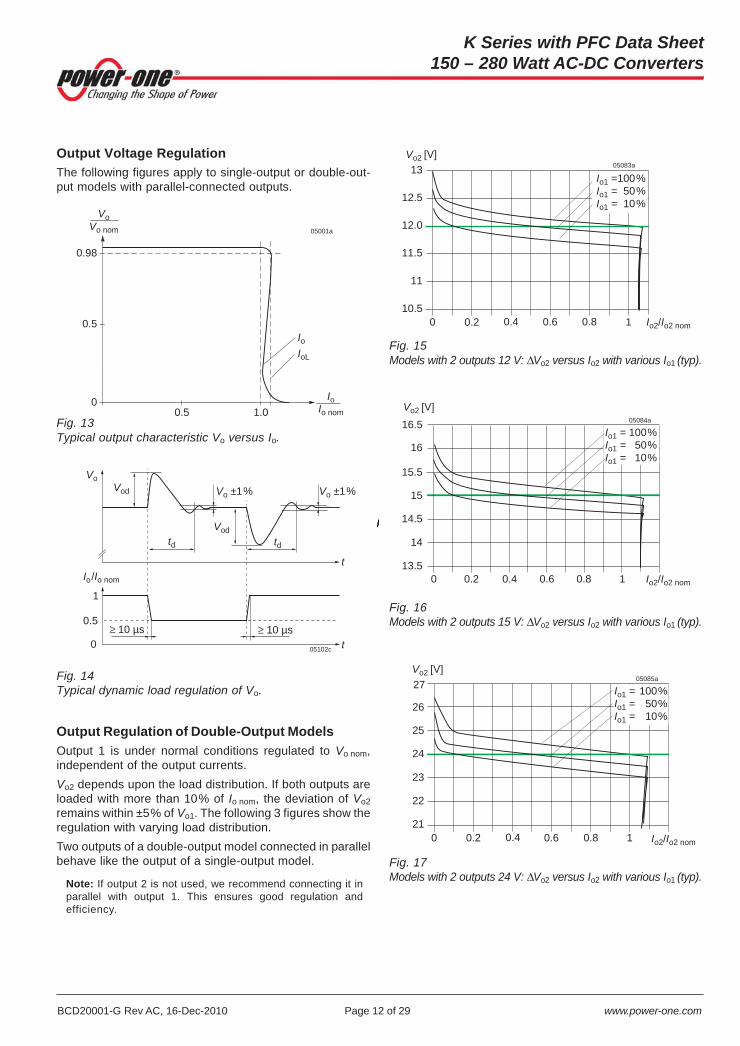
Fig. 15Models with 2 outputs 12 V: ∆Vo2 versus Io2 with various Io1 (typ).
Output Voltage RegulationThe following figures apply to single-output or double-out-put models with parallel-connected outputs.
Fig. 16Models with 2 outputs 15 V: ∆Vo2 versus Io2 with various Io1 (typ).
Fig. 17Models with 2 outputs 24 V: ∆Vo2 versus Io2 with various Io1 (typ).
Fig. 13Typical output characteristic Vo versus Io.
Fig. 14Typical dynamic load regulation of Vo.
Vo
Vo nom
0.98
0.5
00.5 1.0
Io
IoL
Io
Io nom
05001a
Output Regulation of Double-Output ModelsOutput 1 is under normal conditions regulated to Vo nom,independent of the output currents.Vo2 depends upon the load distribution. If both outputs areloaded with more than 10% of Io nom, the deviation of Vo2remains within ±5% of Vo1. The following 3 figures show theregulation with varying load distribution.Two outputs of a double-output model connected in parallelbehave like the output of a single-output model.
Note: If output 2 is not used, we recommend connecting it inparallel with output 1. This ensures good regulation andefficiency.
Vod
Vod
td td
Vo ±1% Vo ±1%
t
t
≥ 10 µs ≥ 10 µs
Vo
0
0.5
1
Io/Io nom
05102c
0 1 Io2/Io2 nom
10.5
11
11.5
12.0
12.5
13
Vo2 [V]
Io1 = 100%
Io1 = 50%
Io1 = 10%
0.2 0.4 0.6 0.8
05083a
0 0.2 0.4 0.6 0.8 1 Io2/Io2 nom
13.5
14
14.5
15
15.5
16
Vo2 [V]
Io1 = 100%
Io1 = 50%
Io1 = 10%
16.505084a
0 0.2 0.4 0.6 0.8 1 Io2/Io2 nom
21
22
23
24
25
26
27
Vo2 [V]
Io1 = 100%
Io1 = 50%
Io1 = 10%
05085a
II
BCD20001-G Rev AC, 16-Dec-2010 Page 13 of 29 www.power-one.com
K Series with PFC Data Sheet150 – 280 Watt AC-DC Converters
S–/Vo1–
i
Vo+
Iinh
Vinh
06031b
14
18
Inp
ut
Auxiliary FunctionsInhibit for Remote On/OffThe outputs may be enabled or disabled by means of alogic signal (TTL, CMOS, etc.) applied between the inhibitinput i (pin 18) and pin 14 (S– or Vo1–). In systems withseveral converters, this feature can be used to control theactivation sequence of the converters. If the inhibit functionis not required, connect the inhibit pin 18 to pin 14.
Note: If pin 18 is not connected, the output is disabled.
Fig. 18Definition of Vinh and Iinh.
Fig. 20Output response as a function of inhibit control
Fig. 19Typical inhibit current I inh versus inhibit voltage Vinh
0 t
t0
Inhibit
1
0.1
1Vo/Vo nom
tr tf
06001
Programmable Output Voltage (R-Function)As a standard feature, the converters offer an adjustableoutput voltage, identified by letter R in the typedesignation. The control input R (pin 16) accepts either acontrol voltage Vext or a resistor Rext to adjust the desiredoutput voltage. When input R is not connected, the outputvoltage is set to Vo nom.a) Adjustment by means of an external control voltage Vext
between pin 16 (R) and pin 14:The control voltage range is 0 – 2.75 VDC and allows anoutput voltage adjustment in the range of approximately0 – 110% Vo nom.
VoVext ≈ –––––– • 2.5 VVo nom
b) Adjustment by means of an external resistor:Depending upon the value of the required output voltagethe resistor shall be connectedeither: Between pin 16 and pin 14 (Vo < Vo nom) toachieve an output voltage adjustment range of approxi-mately 0 – 100% Vo nom.or: Between pin 16 and pin 12 (Vo > Vo nom) to achieve anoutput voltage adjustment range of 100 – 110% Vo nom.
Warning:
– Vext shall never exceed 2.75 V.– The value of R'ext shall never be less than the lowest
value as indicated in table R'ext (for V0 > V0 nom) toprevent the converter from damage!
Sense Lines (Single-Output Models)Important: Sense lines must always be connected!Incorrectly connected sense lines may activate theovervoltage protection resulting in a permanent short-circuitof the output.
This feature allows for compensation of voltage dropsacross the connector contacts and if necessary, across theload lines. We recommend connecting the sense linesdirectly at the female connector.To ensure correct operation, both sense lines (S+, S–)should be connected to their respective power outputs(Vo+ and Vo–), and the voltage difference between anysense line and its respective power output (as measuredon the connector) should not exceed the following values:
Table 9: Maximum voltage compensation allowed usingsense lines
Output Total voltage difference Voltage difference voltage between sense lines and between
their respective outputs Vo– and S–
5.1 V <0.5 V <0.25 V
12 V, 15 V, 24 V <1.0 V <0.25 V
Note: If the output voltages are increased above Vo nom viaR-input control, option P setting, remote sensing or option T,the output currents must be reduced accordingly, so thatPo nom is not exceeded.
Table 8: Inhibit characteristics
Characteristic Conditions min typ max Unit
Vinh Inhibit Vo = on Vi min – Vi max – 50 0.8 Vvoltage Vo = off 2.4 50
I inh Inhibit current Vinh = 0 – 400 µA
t r Rise time 30 ms
t f Fall time depending on Io
1.6
0.8
0
–0.8–50
Vinh [V]
Iinh [mA]
–30 0–10 10 30 50
2.0
1.2
0.4
–0.4
Vinh = 0.8 V
Vo = on Vo = off
Vinh = 2.4 V
06032
BCD20001-G Rev AC, 16-Dec-2010 Page 14 of 29 www.power-one.com
K Series with PFC Data Sheet150 – 280 Watt AC-DC Converters
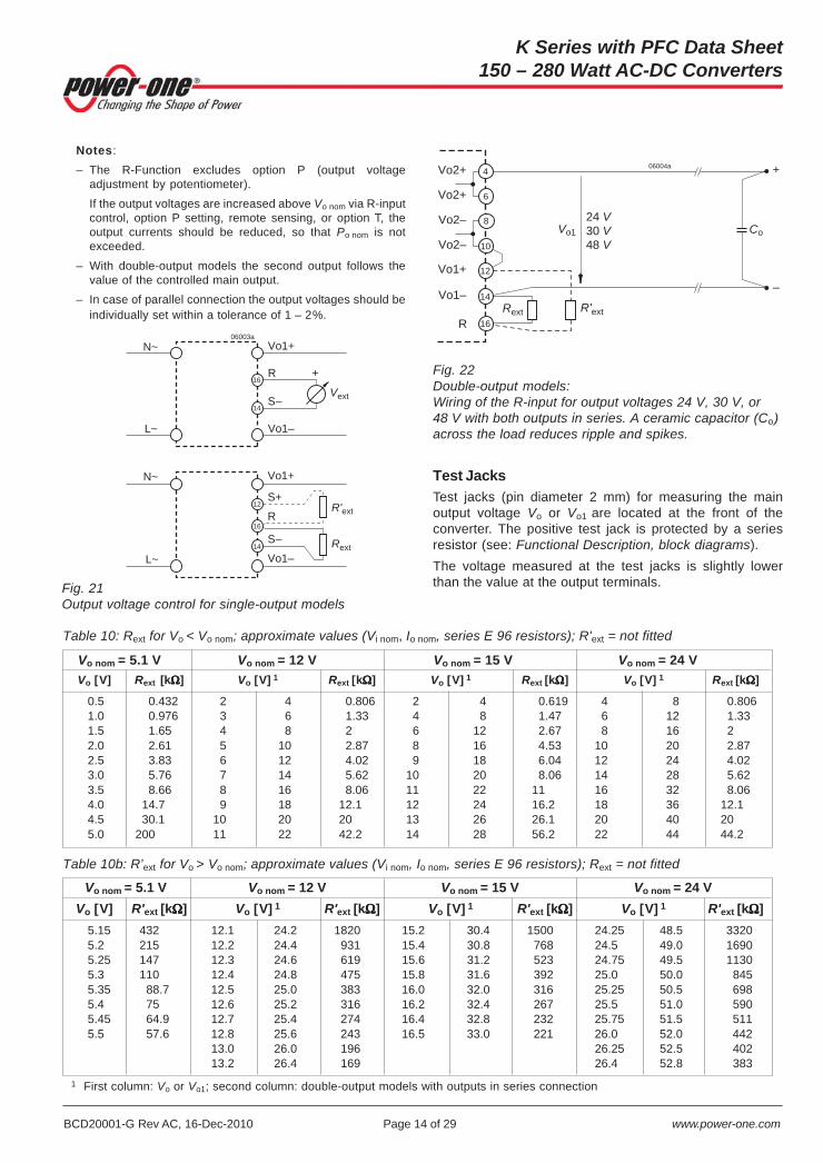
Fig. 21Output voltage control for single-output models
Notes:– The R-Function excludes option P (output voltage
adjustment by potentiometer).If the output voltages are increased above Vo nom via R-inputcontrol, option P setting, remote sensing, or option T, theoutput currents should be reduced, so that Po nom is notexceeded.
– With double-output models the second output follows thevalue of the controlled main output.
– In case of parallel connection the output voltages should beindividually set within a tolerance of 1 – 2%.
Table 10: Rext for Vo < Vo nom; approximate values (Vi nom, Io nom, series E 96 resistors); R'ext = not fitted
Vo nom = 5.1 V Vo nom = 12 V Vo nom = 15 V Vo nom = 24 VVo [V] Rext [kΩΩΩΩΩ] Vo [V] 1 Rext [kΩΩΩΩΩ] Vo [V] 1 Rext [kΩΩΩΩΩ] Vo [V] 1 Rext [kΩΩΩΩΩ]
0.5 0.432 2 4 0.806 2 4 0.619 4 8 0.8061.0 0.976 3 6 1.33 4 8 1.47 6 12 1.331.5 1.65 4 8 2 6 12 2.67 8 16 22.0 2.61 5 10 2.87 8 16 4.53 10 20 2.872.5 3.83 6 12 4.02 9 18 6.04 12 24 4.023.0 5.76 7 14 5.62 10 20 8.06 14 28 5.623.5 8.66 8 16 8.06 11 22 11 16 32 8.064.0 14.7 9 18 12.1 12 24 16.2 18 36 12.14.5 30.1 10 20 20 13 26 26.1 20 40 205.0 200 11 22 42.2 14 28 56.2 22 44 44.2
Table 10b: R’ext for Vo > Vo nom; approximate values (Vi nom, Io nom, series E 96 resistors); Rext = not fitted
Vo nom = 5.1 V Vo nom = 12 V Vo nom = 15 V Vo nom = 24 VVo [V] R'ext [kΩΩΩΩΩ] Vo [V] 1 R'ext [kΩΩΩΩΩ] Vo [V] 1 R'ext [kΩΩΩΩΩ] Vo [V] 1 R'ext [kΩΩΩΩΩ]
5.15 432 12.1 24.2 1820 15.2 30.4 1500 24.25 48.5 33205.2 215 12.2 24.4 931 15.4 30.8 768 24.5 49.0 16905.25 147 12.3 24.6 619 15.6 31.2 523 24.75 49.5 11305.3 110 12.4 24.8 475 15.8 31.6 392 25.0 50.0 8455.35 88.7 12.5 25.0 383 16.0 32.0 316 25.25 50.5 6985.4 75 12.6 25.2 316 16.2 32.4 267 25.5 51.0 5905.45 64.9 12.7 25.4 274 16.4 32.8 232 25.75 51.5 5115.5 57.6 12.8 25.6 243 16.5 33.0 221 26.0 52.0 442
13.0 26.0 196 26.25 52.5 40213.2 26.4 169 26.4 52.8 383
1 First column: Vo or Vo1; second column: double-output models with outputs in series connection
R'extRext
14
16
Vo1–
Vo1+
R
Vo2–
Vo2–
Vo2+
Vo2+
12
10
8
6
4 +
–
Vo1
24 V
30 V
48 V
Co
06004a
Fig. 22Double-output models:Wiring of the R-input for output voltages 24 V, 30 V, or48 V with both outputs in series. A ceramic capacitor (Co)across the load reduces ripple and spikes.
Test JacksTest jacks (pin diameter 2 mm) for measuring the mainoutput voltage Vo or Vo1 are located at the front of theconverter. The positive test jack is protected by a seriesresistor (see: Functional Description, block diagrams).The voltage measured at the test jacks is slightly lowerthan the value at the output terminals.
R
Vo1+
Vo1–
S–Vext
N~
L~
Rext
R'ext
14
16
16
14
+
S+
Vo1+
Vo1–
S–
N~
L~
R
12
06003a
BCD20001-G Rev AC, 16-Dec-2010 Page 15 of 29 www.power-one.com
K Series with PFC Data Sheet150 – 280 Watt AC-DC Converters
Power
supplyLoad
–+
Input Vo–
R
Temperature sensor
ϑ
03099d
Battery
Vo+
+
2.10
2.15
2.20
2.25
2.30
2.35
2.40
2.45Cell voltage [V]
–20 –10 0 10 20 30 40 50 °C
06139b
VC = 2.27 V, –3 mV/K VC = 2.27 V, –3.5 mV/KVC = 2.23 V, –3 mV/K VC = 2.23 V, –3.5 mV/K
Vo safe
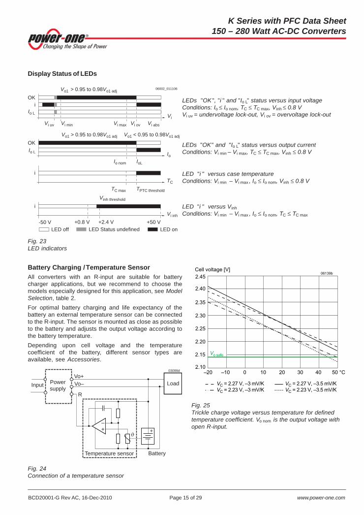
Display Status of LEDs
Battery Charging /Temperature SensorAll converters with an R-input are suitable for batterycharger applications, but we recommend to choose themodels especially designed for this application, see ModelSelection, table 2.For optimal battery charging and life expectancy of thebattery an external temperature sensor can be connectedto the R-input. The sensor is mounted as close as possibleto the battery and adjusts the output voltage according tothe battery temperature.Depending upon cell voltage and the temperaturecoefficient of the battery, different sensor types areavailable, see Accessories.
Fig. 25Trickle charge voltage versus temperature for definedtemperature coefficient. Vo nom is the output voltage withopen R-input.
LEDs "OK ", "i " and "Io L" status versus input voltageConditions: Io ≤ Io nom, TC ≤ TC max, Vinh ≤ 0.8 VVi uv = undervoltage lock-out, Vi ov = overvoltage lock-out
LEDs "OK" and "Io L" status versus output currentConditions: Vi min – Vi max, TC ≤ TC max, Vinh ≤ 0.8 V
LED "i " versus case temperatureConditions: Vi min – Vi max , Io ≤ Io nom, Vinh ≤ 0.8 V
LED "i " versus VinhConditions: Vi min – Vi max , Io ≤ Io nom, TC ≤ TC max
Vo1 > 0.95 to 0.98Vo1 adj
Vi max Vi ovVi minVi uv
Vi
Vi abs
OKi
Vo1 > 0.95 to 0.98Vo1 adj
Io nom IoL
Io
OKIo L
Vo1 < 0.95 to 0.98Vo1 adj
TC
i
TC max TPTC threshold
Vi inh
i
+50 V+0.8 V +2.4 V-50 V
Vinh threshold
Io L
LED off LED onLED Status undefined
06002_011106
Fig. 23LED indicators
Fig. 24Connection of a temperature sensor

BCD20001-G Rev AC, 16-Dec-2010 Page 16 of 29 www.power-one.com
K Series with PFC Data Sheet150 – 280 Watt AC-DC Converters
Table 11: Electromagnetic immunity (type tests)
Phenomenon Standard Level Coupling Value Waveform Source Test In Perf.mode 1 applied imped. procedure oper. crit. 2
Electrostatic IEC/EN 4 contact discharge 8000 Vp 1/50 ns 330 Ω 10 positive and yes Adischarge 61000-4-2 air discharge 15000 Vp
150 pF 10 negative(to case) discharges
Electromagnetic IEC/EN 3 antenna 10 V/m AM 80% n.a. 80 – 1000 MHz yes Afield 61000-4-3 1 kHz
10 V/m 50% duty cycle, n.a. 900 ±5 MHz yes A200 Hz repetition pulse modul.
frequency
Electrical fast IEC/EN 3 capacitive, o/c ±2000 Vp bursts of 5/50 ns 50 Ω 60 s positive yes Atransients/burst 61000-4-4 ±i/c, +i/–i 2.5/5 kHz over 60 s negative
direct 15 ms; burst transients perperiod: 300 ms coupling mode
Surges IEC/EN 3 ±i/c ±2000 Vp 1.2/50 µs 12 Ω 5 pos. and 5 neg. yes A3
61000-4-5 +i/–i 2 Ω surges percoupling mode
Conducted IEC / EN 3 i, o, signal wires 10 VAC AM 80% 150 Ω 0.15 – 80 MHz yes Adisturbances 61000-4-6 (140 dBµV) 1 kHz sine wafe
Voltage dips, IEC/EN 40% +i/–i 230 →92 2→1→2 s n.a. yes B4
short interrup- 6100-4-11 →230tions and 0% +i/–i 230→0 B4variations →230
1 i = input, o = output, c = case2 A = Normal operation, no deviation from specifications, B = Normal operation, temporary loss of function or deviation from
specs possible3 For converters with version V102 or higher. Older LKP models meet only B.4 Only LKP models have been tested.
Emissions
Electromagnetic Compatibility (EMC)A metal oxide VDR together with an input fuse and an inputfilter form an effective protection against high input
Immunity
transient voltages, which typically occur in mostinstallations. The converters have been successfullytested to the following specifications:
Fig. 26aConducted emissions (peak) at the phase input accordingto EN 55011/22, measured at Vi nom and Io nom (LK4301-7R).The neutral line performs quite similar.
10
30
50
70
0.2 0.5 1 2 5 10 20 MHz
dbµV LKP5660-6, Peak L, conducted, 0.15 - 30 MHz, PMM 8000, 30-May-06
LKP
5660-con-p-a
EN 55022 B
Fig. 26bConducted emissions (peak) at the phase input accordingto EN 55011/22, measured at Vi nom and Io nom (LKP5660-7R). The neutral line performs quite similar.
10
30
50
70
0.2 0.5 1 2 5 10 20 MHz
dbµV LK4301-6, Peak L, conducted, 0.15 - 30 MHz, PMM 8000, 30-May-06
LK4301-con-p
EN 55022 B

BCD20001-G Rev AC, 16-Dec-2010 Page 17 of 29 www.power-one.com
K Series with PFC Data Sheet150 – 280 Watt AC-DC Converters
Environmental ConditionsTable 12: Mechanical and climatic stress
Test Method Standard Test Conditions StatusCab Damp heat IEC/EN 60068-2-78:2001 Temperature: 40 ±2 °C Converter not
steady state MIL-STD-810D sect. 507.2 Relative humidity: 93 +2/-3 % operatingDuration: 56 days
Ea Shock IEC/EN 60068-2-27:1987 Acceleration amplitude: 100 gn = 981 m/s2 Converter(half-sinusoidal) MIL-STD-810D sect. 516.3 Bump duration: 6 ms operating
Number of bumps: 18 (3 each direction)
Eb Bump IEC/EN 60068-2-29:1987 Acceleration amplitude: 40 gn = 392 m/s2 Converter(half-sinusoidal) MIL-STD-810D sect. 516.3 Bump duration: 6 ms operating
Number of bumps: 6000 (1000 each direction)
Fc Vibration IEC/EN 60068-2-6:1995 Acceleration amplitude: 0.35 mm (10 – 60 Hz) Converter(sinusoidal) MIL-STD-810D sect. 514.3 5 gn = 49 m/s2 (60 – 2000 Hz) operating
Frequency (1 Oct/min): 10 – 2000 HzTest duration: 7.5 h (2.5 h each axis)
Fh Random vibration IEC/EN 60068-2-64 Acceleration spectral density: 0.05 gn2/Hz Converterbroad band Frequency band: 8 – 500 Hz operating(digital control) Acceleration magnitude: 4.9 gn rms
Test duration: 1.5 h (0.5 h each axis)
Kb Salt mist, cyclic IEC/EN 60068-2-52:1996 Concentration: 5% (30 °C) Converter not(sodium chloride Duration: 2 h per cycle operatingNaCl solution) Storage: 40 °C, 93% rel. humidity
Storage duration: 22 h per cycleNumber of cycles: 3
Table 13: Temperature specifications, values given are for an air pressure of 800 – 1200 hPa (800 – 1200 mbar)
Temperature -5 - 6 -7 - 9Characteristics Conditions min max min max min max min max UnitTA Ambient temperature Converter –251 50 –251 60 –25 71 –40 71 °CTC Case temperature 1 operating –251 853 –251 90 3 –25 953 –40 953
TS Storage temperature Not operating –40 2 100 –402 100 –40 100 –55 100
Temperatures
1 Minimum TA and TC for models with option E is –40 °C.2 Minimum TS for models with option E is –55 °C.3 Overtemperature lockout at TC ≥ 95 °C.
30 50 100 200 500 1000 MHz
10
40
JM070
dBµV/m TÜV-Divina, ESVS 30:R&S, BBA 9106/UHALP 9107:Schwarzb., QP, 2005-11-11Testdistance 10 m, LK4301-7R, Ui=230 VAC, Uo=12 V Io= 12 A
EN 55011 A
<25 dbµV/m
50
20
30
Fig. 27Typ. radiated emissions accord. to EN 55011/22, antenna10 m distance, measured at Vi nom and Io nom (LK4301-7R).

BCD20001-G Rev AC, 16-Dec-2010 Page 18 of 29 www.power-one.com
K Series with PFC Data Sheet150 – 280 Watt AC-DC Converters
159 4.5
89
11
1 (
3U
)
168.5
d
80
4.5
19.7
9.5
29.9
6.5 5
1.5
30.3
20.3
12.1
10.3
7.0
4
3.27
7 TE 9 TE
Test jacks (+/–)
Option P (Vo)
Option D (Vti)
LED OK (green)
LED i (red)
LED IoL (red)
Option D (Vto)
25
.91
1.8
Front plate Main face Back plate
Measuring point ofcase temperature TC
(171.0 .... 171.9)50
09002c
42
Gra
vita
tio
na
la
xis
= Ø 4.1= Ø 3.5
Mounting slots for chassis or wall mounting
Screw holes of the
frontplate
∅5 x 90°
∅2.8 0.2
27.38
Mechanical DataDimensions in mm. The converters are designed to be inserted intoa 19" rack, 160 mm long, according to IEC 60297-3.
Notes:
– d ≥ 15 mm, recommended minimum distanceto next part in order to ensure proper aircirculation at full output power.
– free air location: the converter should bemounted with fins in a vertical position toachieve maximum airflow through the heatsink.Fig. 28
Aluminium case K02 with heat sink, black finish (EPpowder coated), and self cooling; weight ≈1.6 kg
EuropeanProjection
Table 14: MTBF calculated according to MIL-HDBK 217F
Values at specified Model Ground benign Ground fixed Ground mobile Unitcase temperature 40 °C 40 °C 70 °C 50 °C
MTBF LK4301-7ER 514 000 88 000 38 000 35 000 h
Reliability

BCD20001-G Rev AC, 16-Dec-2010 Page 19 of 29 www.power-one.com
K Series with PFC Data Sheet150 – 280 Watt AC-DC Converters
11
1 (
3U
)
17.3 133.4
168
10
1
547.2
1585
M 4
5
Measuring point ofcase temperature TC
50
(171.0 ... 171.9)
3.27
7 TE 4 TE
09003b
38.5
11.8
EuropeanProjection
6.5
11.2
13
140
17.3 133.4 ±0.230
168
5 47.2
38.5
127
6.5
11.8
11027
Fig. 29Option B1: Aluminium case K02 with small cooling plate; black finish (EP powder coated).Suitable for mounting with access from the backside.Total weight approx. 1.2 kg.
Fig. 30Option B: Aluminium case K02 with large cooling plate; black finish (EP powder coated).Suitable for front mounting.Total weight approx. 1.3 kg
Note: Long case with option B2, elongated by 60 mm for220 mm rack depth, is available on request. (No LEDs, notest jacks.)

BCD20001-G Rev AC, 16-Dec-2010 Page 20 of 29 www.power-one.com
K Series with PFC Data Sheet150 – 280 Watt AC-DC Converters
Fig. 31aView of converter's male standard H15connector and the connector H15S4 (modelswith option K)
Table 15: Pin allocation
Pin Connector H15S2/S45 Connector type H15
no. LK4003 (Vo = 5.1 V) LK4000 (Vo ≥≥≥≥≥ 5.1 V) LK/LKP5000
4Vo+ Positive output Vo+ Positive output Vo2+ Pos. output 2
6
8Vo– Negative output Vo– Negative output Vo2– Neg. output 2
10
12 S+ Sense+ S+ Sense+ Vo1+ Pos. output 1
14 S– Sense– S– Sense– Vo1– Neg. output 1
16 R 1 Control of Vo R 1 Control of Vo R 1 Control of Vo1
18 i Inhibit i Inhibit i Inhibit
20 D 3 Save data D 3 Save data D 3 Save dataV 3 ACFAIL
22 T 4 Current share T 4 Current share T 4 Current share
24 2 Protective earth Protective earth Protective earth
26N∼ Neutral line N∼ Neutral line N∼ Neutral line
28 30
L∼ Phase line L∼ Phase line L∼ Phase line32
1 Not connected, if option P is fitted.2 Leading pin (pre-connecting)3 Option D excludes option V and vice versa. Pin not connected, unless
option D or V is fitted.4 Not connected, unless option T is fitted.5 Option K stands for the H15S4 connector (compatibility with LK1001)
4
4/6
32
30/32
Type H15
Type H15S4
Fixtures for connector
retention clips V
(see Accessories)
Fixtures for connector
retention clips V
(see Accessories)
10010a
Safety and Installation Instructions
Connector Pin AllocationThe connector pin allocation table defines theelectrical potentials and the physical pinpositions on the H15 connector. The protectiveearth is connected by a leading pin (no. 24),ensuring that it makes contact with the femaleconnector first.Installation Instructions
S10001c
32 28 24 20 16 12 4/6
30 26 22 18 14 8/10
Fixtures for retention clips
Type H15S2
Installation InstructionsNote: These converters have a power factor correction(PFC). The LK4000/5000 models are intended to replace theLK1000 and LK2000 converters in order to comply with IEC/EN 61000-3-2. LK1000 is replaced by LK4003 with option K.
Switch off the system and check for hazardous voltagesbefore altering any connection!These converters are components, intended exclusivelyfor inclusion within other equipment by an industrialassembly operation or by professional installers.Installation must strictly follow the national safetyregulations in compliance with the enclosure, mounting,creepage, clearance, casualty, markings, and segre-gation requirements of the end-use application.Connection to the system shall be made via the matchingH15 female connector H15; see Accessories. Otherinstallation methods may not meet the safetyrequirements.Pin no. 24 ( ) is reliably connected with the case. Forsafety reasons it is essential to connect this pin reliably toprotective earth. See Safety of Operator-Accessible OutputCircuits.The phase input 30/32 (L~) is connected via a built-in fuse(see Input Fuse and table 4), which is designed to protectin the case of a converter failure.
Fig. 31bView of converter's male connector H15S2(not for new designs). Use option K!

BCD20001-G Rev AC, 16-Dec-2010 Page 21 of 29 www.power-one.com
K Series with PFC Data Sheet150 – 280 Watt AC-DC Converters
An additional external fuse, suitable for the application,might be necessary in the wiring to the other line input 26 /28 (N~) if:
• Local requirements demand an individual fuse in eachsource line
• Phase and neutral of the mains are not defined orcannot be assigned to the corresponding terminals (L~to phase and N~ to neutral).
• Neutral and earth impedance is high or undefined
Notes:
– If the inhibit function is not used, pin no. 18 (i) should beconnected to pin no. 14 (S–/Vo1–) to enable the output(s).
– Do not open the converters, or warranty will be invalidated.
– Due to high current values, the converters provide twointernally parallel contacts for certain paths (pins 4/6, 8/10,26/28 and 30/32). It is recommended to use both femalecontacts in parallel connection order to keep the voltagedrop and the temperature of the contacts low.
– If the second output of double-output models is not used,connect it in parallel with the main output.
Make sure that there is sufficient airflow available forconvection cooling. This should be verified by measuringthe case temperature, when the converter is installed andoperated in the end-use application; see ThermalConsiderations.Ensure that a converter failure (e.g., an internal short-circuit) does not result in a hazardous condition; see alsoSafety of Operator-Accessible Output Circuits.
Standards and ApprovalsThe converters are safety-approved to EN/IEC60950-1, and UL/CSA 60950-1 2nd Ed. (version106 or greater).
The converters correspond to Class I equip-ment and have been evaluated for:
• Building-in • Basic insulation between input and case based on 250
VAC, and double or reinforced insulation between inputand output(s).
• Functional insulation between outputs.
Table 16: Leakage currents
Characteristic Class I Unit
Maximum earth Permissible according to IEC/EN 60950 3.5 mAleakage current Typ. value at 254 V, 50 Hz (LK models) 0.8
Typ. value at 254 V, 50 Hz (LKP models) 0.8
• Overvoltage category II • Pollution degree 2 environment • Max. altitude: 2000 m. • The converters fulfill the requirements of a fire enclosure.All boards of the converters are coated with a protectivelacquer.
The converters are subject to manufacturing surveillancein accordance with the above mentioned UL standardsand ISO 9001:2000. A CB-scheme is available.
Cleaning AgentsIn order to avoid possible damage, any penetration ofcleaning fluids is to be prevented, since the powersupplies are not hermetically sealed.
Protection DegreeCondition: Female connector fitted to the converter. • IP 30: All models except those with option P, and except
those with option D or V including a potentiometer.
• IP 20: All models fitted with option P, or with option D orV with potentiometer.
Leakage CurrentsLeakage currents flow due to internal leakage capacitancesand Y-capacitors. The current values are proportional to thesupply voltage and are specified in the table below.
IsolationThe electric strength test is performed in the factory asroutine test in accordance with EN 50116 and IEC/EN60950 and should not be repeated in the field. Power-Onewill not honor any warranty claims resulting from electricstrength field tests.
Table 17: Isolation
Characteristic Input to case Output(s) to Output 1 to Unitand output(s) case output 2
Electric Factory test >1 s 2.8 1 1.4 0.15 kVDCstrength AC test voltage equivalent 2.0 1.0 0.1 kVACtest to factory testInsulation resistance at 500 VDC >300 >300 >100 2 MΩCreapage distances ≥ 3.2 3 -- -- mm
1 According to EN 50116 and IEC/EN 60950, subassemblies connecting input to output are pre-tested with 5.6 kVDC or 4 kVAC.2 Tested at 150 VDC3 Input to outputs: 6.4 mm

BCD20001-G Rev AC, 16-Dec-2010 Page 22 of 29 www.power-one.com
K Series with PFC Data Sheet150 – 280 Watt AC-DC Converters
Fig. 32Schematic safety concept.
Table 18: Safety concept leading to a SELV output circuit
Conditions AC-DC converter Installation Result
Nominal voltage Grade of insulation Measures to achieve the resulting Safety status of the AC-DCbetween input and output safety status of the output circuit converter output circuitprovided by the AC-DC converter
Mains Double or reinforced Earthed case1 and installation SELV circuit≤ 250 VAC according to the applicable standards
1 The earth connection has to be provided by the installer according to the relevant safety standards, e.g., IEC/EN 60950.
Safety of Operator-Accessible Output CircuitsIf the output circuit of a converter is operator-accessible, itshall be an SELV circuit according to IEC/EN 60950.The table below shows a possible installationconfiguration, compliance with which causes the outputcircuit of a K Series AC-DC converter to be a SELV circuitaccording to IEC/EN 60950 up to a configured output voltageof 36 V (sum of nominal voltages connected in series) .However, it is the sole responsibility of the installer toensure compliance with the applicable safety regulations.
-9 Extended Temperature RangeOption -9 extends the operational ambient temperaturerange from –25 to 71 °C (standard) to – 40 to 71 °C. Thepower supplies provide full nominal output power withconvection cooling. Option -9 excludes inrush currentlimitation by NTC.
E Inrush Current LimitationThe converters exhibit an electronic circuit replacing thestandard built-in NTC, in order to achieve an enhancedinrush current limiting function.
Fig. 33Option E block diagram
Description of OptionsTable 19: Survey of options
Option Function of option Characteristic
-9 Extended operational ambient temperature range TA = – 40 to 71 °C
E Electronic inrush current limitation circuitry Active inrush current limitation
P2 Potentiometer for fine adjustment of output voltage Adjustment range +10/– 60% of Vo nom, excludes R input
D1 Input and/or output undervoltage monitoring circuitry Safe data signal output (D0 – DD)
V1 Input and/or output undervoltage monitoring circuitry ACFAIL signal according to VME specifications (V0, V2, V3)
T Current sharing Interconnect T-pins if paralleling outputs (max 5 converters)
K H15S4 connector for models with 5.1 V output For new designs; provides compatibility with LK1001 models
B, B1, B2 Cooling plate (160 or 220 mm long) Replaces standard heat sink, allowing direct chassis-mounting
G RoHS-compliant for all six substances G is always the last character in the type designation1 Option D excludes option V and vice versa; option V only for 5.1 V outputs.2 Option P is not available for battery charger models.
Input F
ilter
Control
Convert
er
FET
CbRI
Rectifier PF
C -
corr
ect.
11001b
+
Rs
AC-DC
con-
verter
Mains SELV
Earth
connection
+
–
~
~
10021a
Fuse
Fuse
BCD20001-G Rev AC, 16-Dec-2010 Page 23 of 29 www.power-one.com
K Series with PFC Data Sheet150 – 280 Watt AC-DC Converters
Load
1
1
1
2
2
S+
Vo+
Vo–
S–
T
S+
Vo+
Vo–
S–
T
1
Max. 5 converters in parallel connection
1 Lead lines should have equal length and cross
section, and should run in the same cable loom.2 Diodes recommended in redundant operation only
11036b
Converter
Converter
Load
Max. 5 converters in parallel connection
+ –Power bus
Converter
Vo2–
Vo2+
Vo1–
Vo1+
T
Converter
Vo2–
Vo2+
Vo1–
Vo1+
T
11037b
Fig. 36Paralleling of single-output models using option T withthe sense lines connected at the load
Fig. 37Paralleling of double-output models with the outputsconnected in series, and using option T with power bus.The signal at the T pins is referenced to Vo1–.
Fig. 34Typ. inrush current with option EVi = 230 VAC, f i = 50 Hz, Po = Po nom
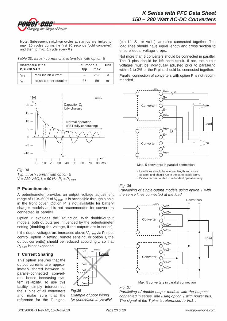
(pin 14: S– or Vo1–), are also connected together. Theload lines should have equal length and cross section toensure equal voltage drops.Not more than 5 converters should be connected in parallel.The R pins should be left open-circuit. If not, the outputvoltages must be individually adjusted prior to parallelingwithin 1 to 2% or the R pins should be connected together.Parallel connection of converters with option P is not recom-mended.
Table 20: Inrush current characteristics with option E
Characteristics all models UnitVi = 230 VAC typ max
I inr p Peak inrush current – 25.3 A
t inr Inrush current duration 35 50 ms
P PotentiometerA potentiometer provides an output voltage adjustmentrange of +10/–60% of Vo nom. It is accessible through a holein the front cover. Option P is not available for batterycharger models and is not recommended for convertersconnected in parallel.Option P excludes the R-function. With double-outputmodels, both outputs are influenced by the potentiometersetting (doubling the voltage, if the outputs are in series).If the output voltages are increased above Vo nom via R inputcontrol, option P setting, remote sensing, or option T, theoutput current(s) should be reduced accordingly, so thatPo nom is not exceeded.
T Current SharingThis option ensures that theoutput currents are approx-imately shared between allparallel-connected convert-ers, hence increasing sys-tem reliability. To use thisfacility, simply interconnectthe T pins of all convertersand make sure that thereference for the T signal
Note: Subsequent switch-on cycles at start-up are limited tomax. 10 cycles during the first 20 seconds (cold converter)and then to max. 1 cycle every 8 s.
15
Ii [A]
10
5
0
–5
–10
0 20 40 60 80 ms
t tinr
Capacitor Ci
fully charged
Normal operation
(FET fully conducting)
20
10 50 7030
11002b
Fig.35Example of poor wiringfor connection in parallel
Vo+
Vo–
Vo+
Vo–
Load
Vo+
Vo–
11003a
BCD20001-G Rev AC, 16-Dec-2010 Page 24 of 29 www.power-one.com
K Series with PFC Data Sheet150 – 280 Watt AC-DC Converters
Vo+/Vo1+
S–/Vo1–
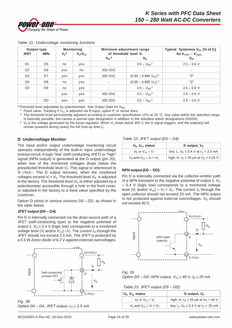
D
VD
ID
Rp
Inp
ut
11007a
NPN open
collector
20
14
D Undervoltage MonitorThe input and/or output undervoltage monitoring circuitoperates independently of the built-in input undervoltagelockout circuit. A logic "low" (self conducting JFET) or "high"signal (NPN output) is generated at the D output (pin 20),when one of the monitored voltages drops below thepreselected threshold level Vt. This signal is referenced toS– /Vo1–. The D output recovers, when the monitoredvoltages exceed Vt + Vh. The threshold level Vbi is adjustedin the factory. The threshold level Vto is either adjusted by apotentiometer accessible through a hole in the front cover,or adjusted in the factory to a fixed value specified by thecustomer.Option D exists in various versions D0 – DD, as shown inthe table below.JFET output (D0 – D4):Pin D is internally connected via the drain-source path of aJFET (self-conducting type) to the negative potential ofoutput 1. VD ≤ 0.4 V (logic low) corresponds to a monitoredvoltage level (Vi and/or Vo1) <Vt. The current ID through theJFET should not exceed 2.5 mA. The JFET is protected bya 0.5 W Zener diode of 8.2 V against external overvoltages.
Fig. 38Option D0 – D4: JFET output, I D ≤ 2.5 mA
Fig. 39Option D5 – DD: NPN output, Vo1 ≤ 40 V, ID ≤ 20 mA
Vo+/Vo1+
S–/Vo1–
D
VD
ID
Rp
Inp
ut
11006a
Self-conducting
junction FET
20
14
Table 21: Undervoltage monitoring functions
Output type Monitoring Minimum adjustment range Typical hysteresis Vho [% of Vt]JFET NPN Vb 4 Vo/Vo1 of threshold level Vt for Vt min – Vt max
Vtb 4 Vto Vho
D1 D5 no yes - 3.5 – VBR 1 2.5 – 0.6 V
D2 D6 yes no 355 VDC - -
D3 D7 yes yes 355 VDC (0.95 – 0.985 Vo1) 2 "0"
D4 D8 no yes - (0.95 – 0.985 Vo1) 2 "0"
D0 D9 no yes - 3.5 – VBR 3 2.5 – 0.6 V
yes yes 355 VDC 3.5 – VBR 3 2.5 – 0.6 V
DD yes yes 355 VDC 3.5 – VBR 1 2.5 – 0.6 V1Threshold level adjustable by potentiometer. See Output Data for VBR.
2 Fixed value. Tracking if Vo1 is adjusted via R-input, option P, or sense lines.3 The threshold level permanently adjusted according to customer specification ±2% at 25 °C. Any value within the specified range
is basically possible, but causes a special type designation in addition to the standard option designations (D0/D9).4 Vb is the voltage generated by the boost regulator. When Vb drops below 355 V, the D signal triggers, and the output(s) will
remain powered during nearly the full hold-up time t h.
Table 22: JFET output (D0 – D4)
Vb, Vo1 status D output, VD
Vb or Vo1 < Vt low, L, VD ≤ 0.4 V at ID = 2.5 mA
Vb and Vo1 > Vt + Vh high, H, ID ≤ 25 µA at VD = 5.25 V
Table 23: JFET output (D5 – DD)
Vb, Vo1 status D output, VD
Vb or Vo1 < Vt high, H, ID ≤ 25 µA at VD = 40 V
Vb and Vo1 > Vt + Vh low, L, VD ≤ 0.4 V at ID = 20 mA
NPN output (D5 – DD):Pin D is internally connected via the collector-emitter pathof a NPN transistor to the negative potential of output 1. VD< 0.4 V (logic low) corresponds to a monitored voltagelevel (Vi and/or Vo1) > Vt + Vh. The current ID through theopen collector should not exceed 20 mA. The NPN outputis not protected against external overvoltages. VD shouldnot exceed 40 V.
BCD20001-G Rev AC, 16-Dec-2010 Page 25 of 29 www.power-one.com
K Series with PFC Data Sheet150 – 280 Watt AC-DC Converters
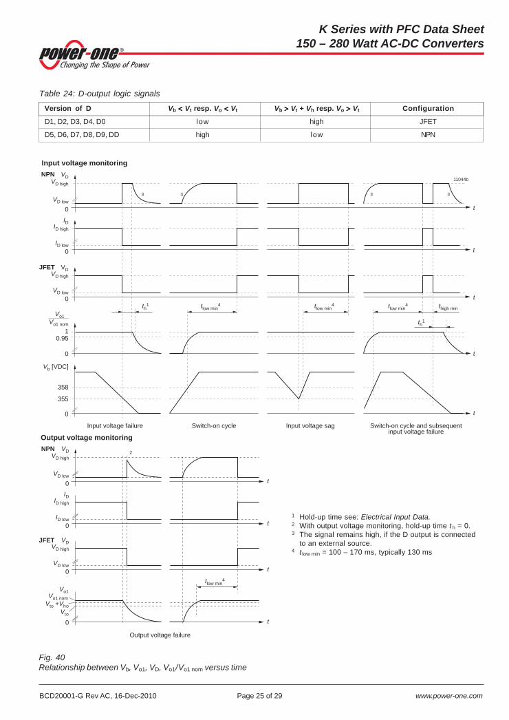
0
10.95
0
Vb [VDC]
0
t
t
t
tlow min
4 tlow min4 thigh min
th1
358
355
Input voltage failure Switch-on cycle Input voltage sag Switch-on cycle and subsequentinput voltage failure
VD high
VD low
VD
0
JFET
NPN
t
Vo1
Vo1 nom
VD high
VD low
VD
tlow min4th
1
0
0
VD high
VD low
VD
0
JFET
NPN
Vo1
VD high
VD low
VD
tlow min4
Vto
Output voltage failure
0
ID high
ID low
ID
t
0
ID high
ID low
ID
t
t
t
t
2
3 3 3 3
Vo1 nom
Vto +Vho
Input voltage monitoring
Output voltage monitoring
11044b
1 Hold-up time see: Electrical Input Data.2 With output voltage monitoring, hold-up time t h = 0.3 The signal remains high, if the D output is connected
to an external source.4 t low min = 100 – 170 ms, typically 130 ms
Fig. 40Relationship between Vb, Vo1, VD, Vo1/Vo1 nom versus time
Table 24: D-output logic signals
Version of D Vb <<<<< Vt resp. Vo <<<<< Vt Vb >>>>> Vt + Vh resp. Vo >>>>> Vt Configuration
D1, D2, D3, D4, D0 low high JFET
D5, D6, D7, D8, D9, DD high low NPN

BCD20001-G Rev AC, 16-Dec-2010 Page 26 of 29 www.power-one.com
K Series with PFC Data Sheet150 – 280 Watt AC-DC Converters
3
5.1 V4.875 V
0
Vb [VDC]
0
t
t
358355
Input voltage failure Switch-on cycle Input voltage sag Switch-on cycle and subsequentinput voltage failure
VV high
VV low
VV
0
V2
t
Vo
0
VV high
VV low
VV
0
V2
Vi
Vti
4
Output voltage failure
0
VV high
VV low
VV
3
Vti + Vhi
tlow min 2 tlow min
2tlow min 2
3 3
44
VV high
VV low
VV
0
V3
t
3
tlow min 2tlow min
2
3 3
th 1
2.0 V
th 1
4
34
tlow min 2
V3
5.1 V4.875 V
0
Vo
2.0 V
Input voltage monitoring
Output voltage monitoring
11045a
t
t
t
t
Fig. 41Vcb, Vo, VV, IV, Vo /Vo nom versus time.
1 VME request: minimum 4 ms2 t low min = 40 – 200 ms, typ 80 ms3 VV level not defined at Vo < 2.0 V4 The V signal drops simultaneously with the output
voltage, if the pull-up resistor R P is connected to Vo+;the V signal remains high if R P is connected to anexternal source.
V ACFAIL Signal (VME)
Available only for models with Vo = 5.1 V.This option defines an undervoltage monitoring circuit forthe input and main output voltage. It generates the ACFAILsignal (V signal) according to the VME standard.
The low state level of the ACFAIL signal is specified at asink current of IV ≤ 48 mA to VV ≤ 0.6 V (open-collectoroutput of an NPN transistor). The pull-up resistor feedingthe open-collector output should be placed on the VMEbackplane.

BCD20001-G Rev AC, 16-Dec-2010 Page 27 of 29 www.power-one.com
K Series with PFC Data Sheet150 – 280 Watt AC-DC Converters
Fig. 42Output configuration of options V2 and V3
After the ACFAIL signal has gone low, the VME standardrequires a hold-up time th of at least 4 ms before the 5.1 Voutput drops at full load to 4.875 V. This hold-up time t h isprovided by the capacitance supporting the boost voltageVb. See Hold-up Time.
Table 25: Undervoltage monitor functions
V output Monitoring Minimum adjustment (VME compatible) Vb Vo1 range of threshold level
Vtb Vto
V2 yes no 355 VDC 1 –
V3 yes yes 355 VDC 1 0.95 – 0.985 Vo1 2
1 Option V monitors Vb generated by the boost regulator. Thetrigger level is adjusted in the factory to 355 VDC.
2 Fixed value between 95% and 98.5% of Vo1
Option V operates independently of the built-in inputundervoltage lockout circuit. A logic "low" signal isgenerated at pin 20, as soon as one of the monitoredvoltages drops below the preselected threshold level Vt.The return for this signal is S– or Vo1–. The V outputrecovers, when the monitored voltage(s) exceed(s) Vt + Vh.The threshold level Vto is adjusted in the factory to acustomer-specified value.V-output (V2, V3):Connector pin V is internally connected to the open collec-tor of an NPN transistor. The emitter is connected to S– orVo1–. VV ≤ 0.6 V (logic low) corresponds to a monitoredvoltage level (Vi and/or Vo) <Vt. The current IV through theopen collector should not exceed 50 mA. The NPN outputis not protected against external overvoltages. VV shouldnot exceed 60 V.
Table 26: Status of V output
Vb, Vo status V output, VV
Vb or Vo < Vt low, L, VV ≤ 0.6 V at IV = 50 mA
Vb and Vo1 > Vt + Vh high, H, IV ≤ 25 µA at VV = 5.1 V
K Connector H15S4Models with 5.1 V output are fitted with a connector H15S4(rather than H15S2). This option should be used for newdesigns and provides compatibility to LK1001 models.
B, B1, B2 Cooling PlateWhere a cooling surface is available, we recommend theuse of a cooling plate instead of the standard heat sink.The mounting system should ensure sufficient coolingcapacity to guarantee that the maximum case tempera-ture TC max is not exceeded. The cooling capacity is calcu-lated by:
(100% – η)PLoss = –––––––––– • Vo • Io
η
Efficiency η see Model Selection
For the dimensions of the cooling plates, see MechnicalData. Option B2 is for customer-specific models withelongated case (for 220 mm DIN-rack depth).
G RoHSModels with G as last character of the type designation areRoHS-compliant for all six substances.
Vo+
S–
V
VV
IV
Rp
Input
11009a
NPN open
collector
20
14

BCD20001-G Rev AC, 16-Dec-2010 Page 28 of 29 www.power-one.com
K Series with PFC Data Sheet150 – 280 Watt AC-DC Converters
H15, H15S2, and H15S4female connectors withcode key system
AccessoriesA variety of electrical and mechanical accessories areavailable including:– Front panels for 19" DIN-rack: Schroff 16 TE /3U
[HZZ00831] and 16 TE /6U [HZZ00832], or Intermas16 TE /3U [HZZ00731]
– Mating connectors H15, H15S2, and H15S4 withscrew, solder, faston, or press-fit terminals.
– Coding clips for connector coding [HZZ00202]– Connector retention clips (2x) [HZZ01209]– Connector retention brackets CRB HKMS [HZZ01216]– DIN-rail mounting assembly DMB-K/S [HZZ0615]
Different front panels
Connector retention bracketsCRB HKMS
20 to 30 Ncm
Connectorretention clip
DIN-rail mountingassembly DMB-K/S
BCD20001-G Rev AC, 16-Dec-2010 Page 29 of 29 www.power-one.com
K Series with PFC Data Sheet150 – 280 Watt AC-DC Converters
56 (2.2")L
L = 2 m (standard length) other cable lengths on request
adhesive tape
26 (1.02")
9.8
(0.4
")09125a
Metallic cable hood providing fireprotection
Wall-mounting plateMOUNTINGPLATE-K02
Battery temperature sensor
EuropeanProjection
– Cable connector housing (cable hood) KSG-H15/H15S4 [HZZ00141] as screw version. Also availableas retention clip version [HZZ00142], or as a fullymetallic housing.
– Wall-mounting plate K02 [HZZ01213] for models withoption B1
– Additional external input and output filters– Different battery sensors [S-KSMH...] for using the
converter as a battery charger. Different cellcharacteristics can be selected; see BatteryCharging / Temperature Sensor
For additional accessory product information, see theaccessory data sheets listed with each product seriesor individual model listing at www.power-one.com.
NUCLEAR AND MEDICAL APPLICATIONS - Power-One products are not designed, intended for use in, or authorized for use as criticalcomponents in life support systems, equipment used in hazardous environments, or nuclear control systems without the express writtenconsent of the respective divisional president of Power-One, Inc.
TECHNICAL REVISIONS - The appearance of products, including safety agency certifications pictured on labels, may change dependingon the date manufactured. Specifications are subject to change without notice.