lm10524 triple buck power management unit … snvs986a –august 2013–revised january 2014 lm10524...
TRANSCRIPT

LM10524
www.ti.com SNVS986A –AUGUST 2013–REVISED JANUARY 2014
LM10524 Triple Buck Power Management UnitCheck for Samples: LM10524
1FEATURES DESCRIPTIONLM10524 is an advanced PMU containing three
2• Three Highly Efficient Programmable Buckconfigurable, high-efficiency buck regulators forRegulatorssupplying variable voltages. The device is ideal for
– Integrated FETs with Low RDSON supporting ASIC and SOC designs for SSD and– Bucks Operate with Their Phases Shifted to Flash drives.
Reduce the Input Current Ripple and The LM10524 can operate cooperatively with anCapacitor Size ASIC to optimize the supply voltage for low-power– Programmable Output Voltage via the SPI conditions and to control power saving modes via the
Interface SPI interface.– Over and Under-Voltage-Lockout
KEY SPECIFICATIONS– Automatic Internal Soft Start with Power-• Single input rail with wide range: 3.3 to 5.5VOn-Reset• Programmable Buck Regulator Outputs:– Current Overload and Thermal Shutdown
Protection – Buck 1: 1.1V to 3.6V; 1.6A– PFM Mode for High Efficiency at Light Load – Buck 2: 1.1V to 3.6V; 1A
Conditions – Buck 3: 0.7V to 1.95V; 2.5A• Power-Down Data Protection Enhances Data • ±3% feedback voltage accuracy
Integrity • Up to 95% efficient buck regulators• Bypass Mode Available on Buck 1 • 2MHz switching frequency for smaller inductor• Sleep Mode to Save Power During Idle Times size
– DEVSLP Function • 2.815mm, 3.215mm, 0.4mm pitch, 46 bump• SPI-Programmable Interrupt Comparator (2.0V micro SMD package
to 4.0V)• Factory Programmable Startup Sequencing for
Varied Controllers• Fast Startup for all Voltage Rails in about
3.5ms to PWR_OK• Fast Turn-off / Active Discharge on Regulator
Outputs
APPLICATION• Solid-State Drives
1
Please be aware that an important notice concerning availability, standard warranty, and use in critical applications ofTexas Instruments semiconductor products and disclaimers thereto appears at the end of this data sheet.
2All trademarks are the property of their respective owners.PRODUCTION DATA information is current as of publication date. Copyright © 2013–2014, Texas Instruments IncorporatedProducts conform to specifications per the terms of the TexasInstruments standard warranty. Production processing does notnecessarily include testing of all parameters.

C147uF
L3
1.0uH
1.1 to 3.6V, 1.6A
0.7 to 1.95V, 2.5AC6
4.7uF
L1
2.2uHBUCK1
BUCK2
BUCK3
SPI
CO
NT
RO
L LO
GIC
an
d R
EG
IST
ER
S
SW_B3
FB_B3
VIN_B3
FB_B2
SW_B2
VIN_B2
SW_B1
VIN_B1 FB_B1
SPI_CS
SPI_CLKSPI_DOSPI_DI
VIN
GN
D
IRQ
Vcomp
L2
2.2uH
1.1 to 3.6V, 1.0A
C74.7uF
C54.7uF
C82.2uF
Host 3DomainVcore1.0V
Host 1FlashVcc
2.85V
ASIC / SoC
Host 2Domain
Vccq1.8V
LM10524
SystemControl
C2
47uF
C3
47uF
COMP
DEVSLP_OVR2
DEVSLP_OVR1
GN
D
VIN_IO
C42.2uF
IO InputSupply
DEVSLPPOWERUP_MODE
DEVSLP_ CTRL
PWR_OK
Power Supply3.3 / 5.5V
GN
D
SLEEP_EN
LM10524
SNVS986A –AUGUST 2013–REVISED JANUARY 2014 www.ti.com
Typical Application Diagram
2 Copyright © 2013–2014, Texas Instruments Incorporated
Product Folder Links: LM10524
LM10524
www.ti.com SNVS986A –AUGUST 2013–REVISED JANUARY 2014
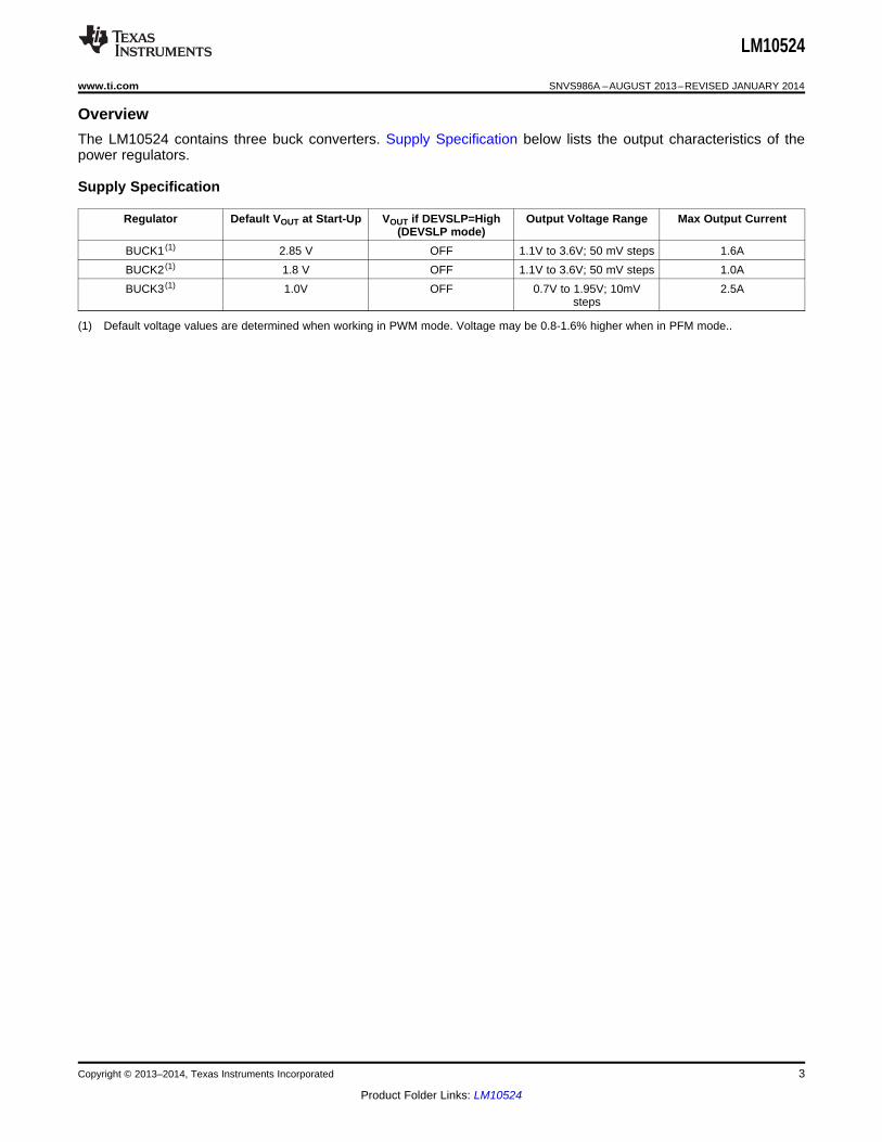
OverviewThe LM10524 contains three buck converters. Supply Specification below lists the output characteristics of thepower regulators.
Supply Specification
Regulator Default VOUT at Start-Up VOUT if DEVSLP=High Output Voltage Range Max Output Current(DEVSLP mode)
BUCK1 (1) 2.85 V OFF 1.1V to 3.6V; 50 mV steps 1.6ABUCK2 (1) 1.8 V OFF 1.1V to 3.6V; 50 mV steps 1.0ABUCK3 (1) 1.0V OFF 0.7V to 1.95V; 10mV 2.5A
steps
(1) Default voltage values are determined when working in PWM mode. Voltage may be 0.8-1.6% higher when in PFM mode..
Copyright © 2013–2014, Texas Instruments Incorporated 3
Product Folder Links: LM10524

GND_B3
SLEEP_EN
DEVSLP_CTRL
DEVSLP_OVR2
DEVSLP_OVR1
GND_B1
GND_B1
SW_B3
SW_B3
SW_B1
SW_B1
VIN_B3
VIN_B1
VIN_B1
FREE
FB_B1
DEVSLP
VIN_B2
VCOMP
VIN
SW_B2
SW_B2
GND
PWR_OK
GND_B2
SPI_CS
SPI_DO
SPI_DI
SPI_CLK
TOP VIEW LOOKING THROUGH THE PACKAGE
FB_B3FREEFB_B2
GND
VIN_IO
GND_B3SW_B3VIN_B3POWER
UP_MODEVIN_B2SW_B2GND_B2
FREEFB_B1FB_B1IRQGND
A
B
C
D
E
F
G
H
1 2 3 4 5 6 7
LM10524
SNVS986A –AUGUST 2013–REVISED JANUARY 2014 www.ti.com
Connection Diagram And Package Marking
Figure 1. 46 Bump Micro SMD with 0.4mm Pitch
4 Copyright © 2013–2014, Texas Instruments Incorporated
Product Folder Links: LM10524

LM10524
www.ti.com SNVS986A –AUGUST 2013–REVISED JANUARY 2014
Table 1. 9.0 LM10524 Pin DescriptionPin # Pin Name I/O (1) Type (2) Functional Description
A4 DEVSLP I D Digital Input Control Signal for entering Device Sleep Mode. Input activates the devicesleep function in conjunction with DEVSLP_OVR1, DEVSLP_OVR2, and PowerUp_mode.This is an active High pin with an option for an internal pullup resistor. Turns off all outputsand internal oscillator.
E7 DEVSLP_CTRL O D Indicates DevSLP signal is active but drives low when device is in SLEEP mode.C7 DEVSLP_OVR1 I D Used to gate activation of device sleep.D7 DEVSLP_OVR2 I D Used to gate activation of device sleep.C5 FB_B1 I/O A Buck Switcher Regulator 1 - Voltage output feedback plus Bypass Power.B4 FB_B1 I/O A Buck Switcher Regulator 1 - Voltage output feedback plus Bypass Power.C4 FB_B1 I/O A Buck Switcher Regulator 1 - Voltage output feedback plus Bypass Power.F3 FB_B2 I A Buck Switcher Regulator 2 - Voltage output feedback.F5 FB_B3 I A Buck Switcher Regulator 3 - Voltage output feedback.C6 FREE Not Used.F4 FREE Not Used.G4 FREE Not Used.B1 GND G G Ground. Connect to system Ground.B2 GND G G Ground. Connect to system Ground.C2 GND G G Ground. Connect to system Ground.A7 GND_B1 G P Buck Switcher Regulator 1 - Power ground for Buck Regulator.B7 GND_B1 G P Buck Switcher Regulator 1 - Power ground for Buck Regulator.G1 GND_B2 G P Buck Switcher Regulator 2 - Power ground for Buck Regulator.H1 GND_B2 G P Buck Switcher Regulator 2 - Power ground for Buck Regulator.G7 GND_B3 G P Buck Switcher Regulator 3 - Power ground for Buck Regulator.H7 GND_B3 G P Buck Switcher Regulator 3 - Power ground for Buck Regulator.C3 IRQ O D Interrupt. Digital Output of Comparator to signal interrupt condition.A2 PWR_OK O D PWR_OK Signal, Push Pull output.H4 POWERUP I/O D Used to indicate SSD initialization is complete. Once initialization is complete, this pin
_MODE should be externally pulled low to allow Sleep mode activation via DEVSLPF7 SLEEP_EN O D Active high output indicates device is in Sleep Mode.C1 SPI_CLK I D SPI Interface - serial clock input.F1 SPI_CS I D SPI Interface - chip select.D1 SPI_DI I D SPI Interface - serial data input.E1 SPI_DO O D SPI Interface - serial data output.A6 SW_B1 I/O P Buck Switcher Regulator 1 - Power Switching node, connect to inductor.B6 SW_B1 I/O P Buck Switcher Regulator 1 - Power Switching node, connect to inductor.F2 SW_B2 I/O P Buck Switcher Regulator 2 - Power Switching node, connect to inductor.G2 SW_B2 I/O P Buck Switcher Regulator 2 - Power Switching node, connect to inductor.H2 SW_B2 I/O P Buck Switcher Regulator 2 - Power Switching node, connect to inductor.F6 SW_B3 I/O P Buck Switcher Regulator 3 - Power Switching node, connect to inductor.G6 SW_B3 I/O P Buck Switcher Regulator 3 - Power Switching node, connect to inductor.H6 SW_B3 I/O P Buck Switcher Regulator 3 - Power Switching node, connect to inductor.B3 VCOMP I A Analog Input for Comparator.A3 VIN I P Power supply Input Voltage — must be present for device to work; decouple closely to D7.A5 VIN_B1 I P Buck Switcher Regulator 1 - Power supply voltage input for power stage PFET, if Buck 1 is
not used, tie to ground to reduce leakage.B5 VIN_B1 I P Buck Switcher Regulator 1 - Power supply voltage input for power stage PFET, if Buck 1 is
not used, tie to ground to reduce leakage.
(1) I: Input Pin, O: Output Pin(2) A: Analog Pin, D: Digital Pin, G: Ground, P: Power Connection
Copyright © 2013–2014, Texas Instruments Incorporated 5
Product Folder Links: LM10524
LM10524
SNVS986A –AUGUST 2013–REVISED JANUARY 2014 www.ti.com
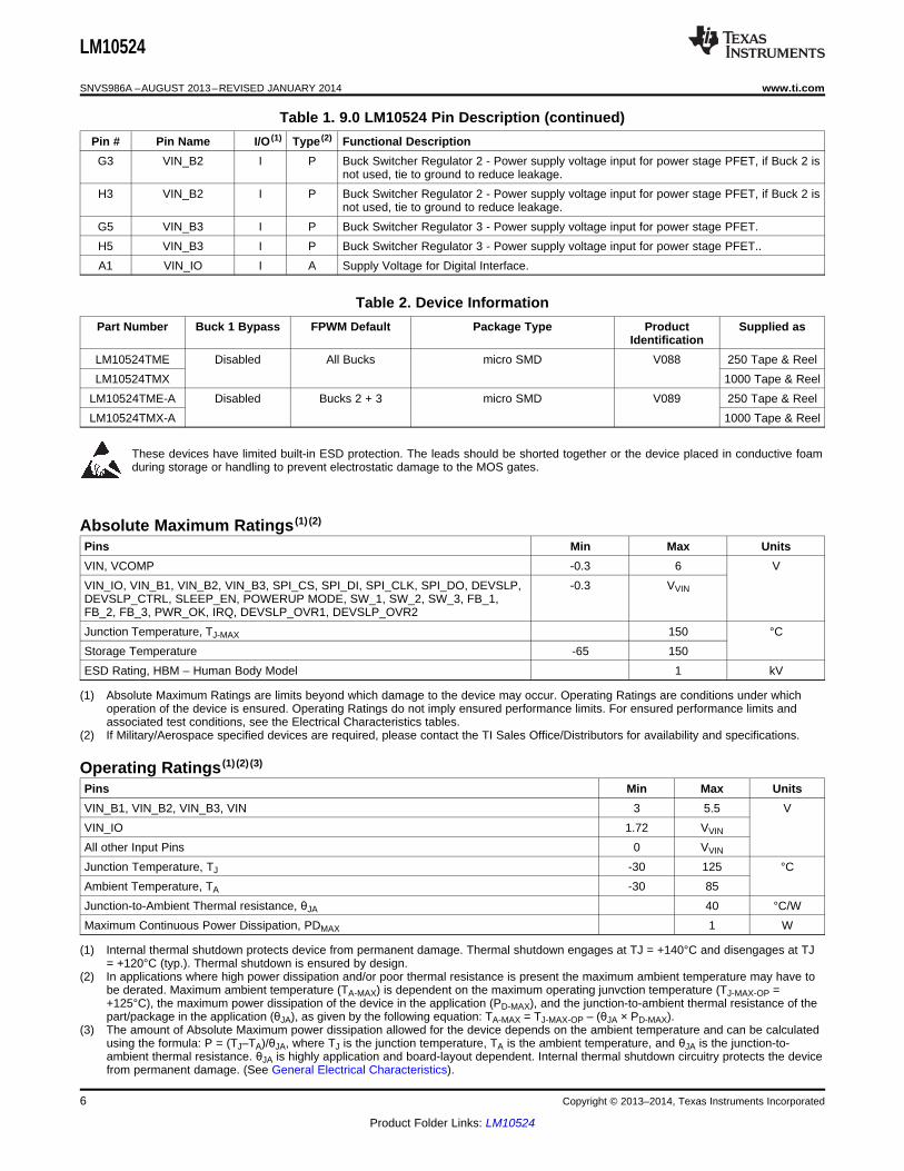
Table 1. 9.0 LM10524 Pin Description (continued)Pin # Pin Name I/O (1) Type (2) Functional DescriptionG3 VIN_B2 I P Buck Switcher Regulator 2 - Power supply voltage input for power stage PFET, if Buck 2 is
not used, tie to ground to reduce leakage.H3 VIN_B2 I P Buck Switcher Regulator 2 - Power supply voltage input for power stage PFET, if Buck 2 is
not used, tie to ground to reduce leakage.G5 VIN_B3 I P Buck Switcher Regulator 3 - Power supply voltage input for power stage PFET.H5 VIN_B3 I P Buck Switcher Regulator 3 - Power supply voltage input for power stage PFET..A1 VIN_IO I A Supply Voltage for Digital Interface.
Table 2. Device InformationPart Number Buck 1 Bypass FPWM Default Package Type Product Supplied as
IdentificationLM10524TME Disabled All Bucks micro SMD V088 250 Tape & ReelLM10524TMX 1000 Tape & Reel
LM10524TME-A Disabled Bucks 2 + 3 micro SMD V089 250 Tape & ReelLM10524TMX-A 1000 Tape & Reel
These devices have limited built-in ESD protection. The leads should be shorted together or the device placed in conductive foamduring storage or handling to prevent electrostatic damage to the MOS gates.
Absolute Maximum Ratings (1) (2)
Pins Min Max UnitsVIN, VCOMP -0.3 6 VVIN_IO, VIN_B1, VIN_B2, VIN_B3, SPI_CS, SPI_DI, SPI_CLK, SPI_DO, DEVSLP, -0.3 VVINDEVSLP_CTRL, SLEEP_EN, POWERUP MODE, SW_1, SW_2, SW_3, FB_1,FB_2, FB_3, PWR_OK, IRQ, DEVSLP_OVR1, DEVSLP_OVR2Junction Temperature, TJ-MAX 150 °CStorage Temperature -65 150ESD Rating, HBM – Human Body Model 1 kV
(1) Absolute Maximum Ratings are limits beyond which damage to the device may occur. Operating Ratings are conditions under whichoperation of the device is ensured. Operating Ratings do not imply ensured performance limits. For ensured performance limits andassociated test conditions, see the Electrical Characteristics tables.
(2) If Military/Aerospace specified devices are required, please contact the TI Sales Office/Distributors for availability and specifications.
Operating Ratings (1) (2) (3)
Pins Min Max UnitsVIN_B1, VIN_B2, VIN_B3, VIN 3 5.5 VVIN_IO 1.72 VVIN
All other Input Pins 0 VVIN
Junction Temperature, TJ -30 125 °CAmbient Temperature, TA -30 85Junction-to-Ambient Thermal resistance, θJA 40 °C/WMaximum Continuous Power Dissipation, PDMAX 1 W
(1) Internal thermal shutdown protects device from permanent damage. Thermal shutdown engages at TJ = +140°C and disengages at TJ= +120°C (typ.). Thermal shutdown is ensured by design.
(2) In applications where high power dissipation and/or poor thermal resistance is present the maximum ambient temperature may have tobe derated. Maximum ambient temperature (TA-MAX) is dependent on the maximum operating junvction temperature (TJ-MAX-OP =+125°C), the maximum power dissipation of the device in the application (PD-MAX), and the junction-to-ambient thermal resistance of thepart/package in the application (θJA), as given by the following equation: TA-MAX = TJ-MAX-OP – (θJA × PD-MAX).
(3) The amount of Absolute Maximum power dissipation allowed for the device depends on the ambient temperature and can be calculatedusing the formula: P = (TJ–TA)/θJA, where TJ is the junction temperature, TA is the ambient temperature, and θJA is the junction-to-ambient thermal resistance. θJA is highly application and board-layout dependent. Internal thermal shutdown circuitry protects the devicefrom permanent damage. (See General Electrical Characteristics).
6 Copyright © 2013–2014, Texas Instruments Incorporated
Product Folder Links: LM10524

LM10524
www.ti.com SNVS986A –AUGUST 2013–REVISED JANUARY 2014
General Electrical Characteristics (1) (2)
Unless otherwise noted, VVIN = 5.0V where: VVIN=VVIN_B1 = VVIN_B2 = VVIN_B3. VVIN_I0 = 3.0V.The application circuit used is the one shown in “Typical Application Circuit".Limits in standard typeface are for TJ = 25°C.Limits in boldface type apply over the full operating junction temperature range of -30°C ≤ TA=TJ ≤ +85°C.Symbol Parameter Conditions Min Typ Max UnitsIQ(DEVSLP) Quiescent supply DevSLP=High 50 200 µA
current. No load.UNDER/OVER VOLTAGE LOCK OUTVUVLO_RISING 2.7 2.9 3.135 VVUVLO_FALLING 2.45 2.6 2.75VOVLO_RISING 6.05VOVLO_FALLING 5.75DIGITAL INTERFACEVIL Logic Input Low SPI_CS, SPI_DI, SPI_CLK, 0.3*VVIN_IO V
POWERUP_MODEVIH Logic Input High 0.7*VVIN_IO(3)
VIL Logic Input Low DEVSLP_OVR1, DEVSLP_OVR2 0.3*VVIN(3)
VIH Logic Input High 0.7*VVIN
VIL Logic Input Low DEVSLP (3) 0.3VVIH Logic Input High 1.2VVOL Logic output Low IRQ (at 2mA load), SPI_DO, 0.2*VVIN_IO
DEVSLP_CTRL (3), SLEEP_EN (3),PWR_OKVOH Logic output High 0.8*VVIN_IO
IIL Input Current, pin SPI_CS, SPI_DI, SPI_CLK -2 µAdriven low DEVSLP -5
IIH Input Current, pin SPI_CS, SPI_DI, SPI_CLK,DEVSLP 2driven high
fSPI_MAX SPI max 10 MHzfrequency
(1) All limits are ensured by design, test and/or statistical analysis. All electrical characteristics having room-temperature limits are testedduring production with TJ = 25°C. All hot and cold limits are ensured by correlating the electrical characteristics to process andtemperature variations and applying statistical process control.
(2) Capacitors: Low-ESR Surface-Mount Ceramic Capacitors (MLCCs) are used in setting electrical characteristics.(3) Specification ensured by design. Not tested during production.
Copyright © 2013–2014, Texas Instruments Incorporated 7
Product Folder Links: LM10524

LM10524
SNVS986A –AUGUST 2013–REVISED JANUARY 2014 www.ti.com
Buck 1 Electrical Characteristics (1) (2) (3)
Unless otherwise noted, VVIN = 5.0V where: VVIN=VVIN_B1 = VVIN_B2 = VVIN_B3.The application circuit used is the one shown in “Typical Application Circuit".Limits in standard typeface are for TJ = 25°C.Limits in boldface type apply over the full operating junction temperature range of -30°C ≤ TA=TJ ≤ +85°C.Symbol Parameter Conditions Min Typ Max UnitsIQ DC Bias Current in VIN No Load, PFM Mode 15 50 µAIOUT-MAX Continuous maximum load Buck 1 enabled, switching in PWM 1.6 A
current (4) (5) (6)
IPEAK Peak switching current limit Buck 1 enabled, switching in PWM 1.9 2.2 2.8η Efficiency peak, Buck 1 (4) IOUT = 0.3 A, VVIN = 3.3V 90 %FSW Switching Frequency 1.75 2 2.3 MHzCIN Input Capacitor (4) 0mA ≤ IOUT ≤ IOUT-MAX 4.7 µFCOUT Output Filter Capacitor (4) 22 47 100
Output Capacitor ESR (4) 20 mΩL Output Filter Inductance (4) 2.2 µH∆VOUT DC Line regulation (4) 3.3V ≤ VVIN ≤ 5V, IOUT = IOUT-MAX 0.5 %/V
DC Load regulation, PWM (4) VVIN=3.3V, 0.1 * IOUT-MAX ≤ IOUT ≤ 0.3 %/AIOUT-MAX
IFB Feedback pin input bias VFB = 2.85V 2.3 5 µAcurrent
VFB Feedback Accuracy VFB = 2.85V -3 3 %RDS-ON-HS High Side Switch On 115 mΩ
Resistance VVIN = 2.6V 190RDS-ON-LS Low Side Switch On 60 110
ResistanceRDS-ON-BYPASS Bypass FET on resistance Used in parallel with the high side
FET while in Bypass mode.Resistance (DCR) of inductor = 100mΩVIN = 3.1V 75 mΩVIN = 2.6V 120
StartupTstart_NoLoad Internal soft-start (turn on Start up from shutdown, VOUT=0V, 0.1 ms
time) (4) no load, LC = recommended circuit,using software enable, to VOUT =95% of final value
Tstart_FullLoad Internal soft-start (turn on Start up from shutdown, VOUT 0.5time) (4) =0V, Maximum Load, LC =
recommended circuit, usingsoftware enable, to VOUT = 95% offinal value
(1) All limits are ensured by design, test and/or statistical analysis. All electrical characteristics having room-temperature limits are testedduring production with TJ = 25°C. All hot and cold limits are ensured by correlating the electrical characteristics to process andtemperature variations and applying statistical process control.
(2) Capacitors: Low-ESR Surface-Mount Ceramic Capacitors (MLCCs) are used in setting electrical characteristics.(3) BUCK normal operation is ensured if VIN ≥ VOUT+1.0V.(4) Specification ensured by design. Not tested during production.(5) In applications where high power dissipation and/or poor thermal resistance is present the maximum ambient temperature may have to
be derated. Maximum ambient temperature (TA-MAX) is dependent on the maximum operating junction temperature (TJ-MAX-OP = +125°C),the maximum power dissipation of the device in the application (PD-MAX), and the junction-to-ambient thermal resistance of thepart/package in the application (θJA), as given by the following equation: TA-MAX = TJ-MAX-OP – (θJA × PD-MAX).
(6) The amount of Absolute Maximum power dissipation allowed for the device depends on the ambient temperature and can be calculatedusing the formula: P = (TJ–TA)/θJA, where TJ is the junction temperature, TA is the ambient temperature, and θJA is the junction-to-ambient thermal resistance. θJA is highly application and board-layout dependent. Internal thermal shutdown circuitry protects the devicefrom permanent damage. (See General Electrical Characteristics.)
8 Copyright © 2013–2014, Texas Instruments Incorporated
Product Folder Links: LM10524

LM10524
www.ti.com SNVS986A –AUGUST 2013–REVISED JANUARY 2014
Buck 2 Electrical Characteristics (1) (2) (3)
Unless otherwise noted, VVIN = 5.0V where: VVIN=VVIN_B1 = VVIN_B2 = VVIN_B3.The application circuit used is the one shown in “Typical Application Circuit".Limits in standard typeface are for TJ = 25°C.Limits in boldface type apply over the full operating junction temperature range of -30°C ≤ TA=TJ ≤ +85°C.Symbol Parameter Conditions Min Typ Max UnitsIQ DC Bias Current in VIN No Load, PFM Mode 15 50 µAIOUT-MAX Continuous maximum load Buck 2 enabled, switching in PWM 1 A
current (4) (5) (6)
IPEAK Peak switching current limit Buck 2 enabled, switching in PWM 1.35 1.55 1.90η Efficiency peak, Buck2 (4) IOUT = 0.3 A, VVIN = 3.3V 90 %FSW Switching Frequency 1.75 2 2.3 MHzCIN Input Capacitor (4) 0mA ≤ IOUT ≤ IOUT-MAX 4.7 µFCOUT Output Filter Capacitor (4) 22 47 100
Output Capacitor ESR (4) 20 mΩL Output Filter Inductance (4) 2.2 µH∆VOUT DC Line regulation (4) 3.3V ≤ VVIN ≤ 5V, IOUT = IOUT-MAX 0.5 %/V
DC Load regulation, PWM (4) V VIN=3.3V, 100mA ≤ IOUT ≤ IOUT-MAX 0.3 %/AIFB Feedback pin input bias VFB = 1.8V 2.3 5 µA
currentVFB Feedback Accuracy VFB = 1.8V -3 3 %RDS-ON-HS High Side Switch On 125 mΩ
ResistanceVVIN = 2.6V 200
RDS-ON-LS Low Side Switch On 60 110Resistance
StartupTstart_NoLoad Internal soft-start (turn on Start up from shutdown, VOUT=0V, no 0.1 ms
time) (4) load, LC = recommended circuit, usingsoftware enable, to VOUT = 95% offinal value
Tstart_FullLoad Internal soft-start (turn on Start up from shutdown, VOUT =0V, 0.5time) (4) Maximum Load, LC = recommended
circuit, using software enable, toVOUT = 95% of final value
(1) All limits are ensured by design, test and/or statistical analysis. All electrical characteristics having room-temperature limits are testedduring production with TJ = 25°C. All hot and cold limits are ensured by correlating the electrical characteristics to process andtemperature variations and applying statistical process control.
(2) Capacitors: Low-ESR Surface-Mount Ceramic Capacitors (MLCCs) are used in setting electrical characteristics.(3) BUCK normal operation is ensured if VIN ≥ VOUT+1.0V.(4) Specification ensured by design. Not tested during production.(5) In applications where high power dissipation and/or poor thermal resistance is present the maximum ambient temperature may have to
be derated. Maximum ambient temperature (TA-MAX) is dependent on the maximum operating junction temperature (TJ-MAX-OP = +125°C),the maximum power dissipation of the device in the application (PD-MAX), and the junction-to-ambient thermal resistance of thepart/package in the application (θJA), as given by the following equation: TA-MAX = TJ-MAX-OP – (θJA × PD-MAX).
(6) The amount of Absolute Maximum power dissipation allowed for the device depends on the ambient temperature and can be calculatedusing the formula: P = (TJ–TA)/θJA, where TJ is the junction temperature, TA is the ambient temperature, and θJA is the junction-to-ambient thermal resistance. θJA is highly application and board-layout dependent. Internal thermal shutdown circuitry protects the devicefrom permanent damage. (See General Electrical Characteristics.)
Copyright © 2013–2014, Texas Instruments Incorporated 9
Product Folder Links: LM10524

LM10524
SNVS986A –AUGUST 2013–REVISED JANUARY 2014 www.ti.com
Buck 3 Electrical Characteristics (1) (2) (3)
Unless otherwise noted, VVIN = 5.0V where: VVIN=VVIN_B1 = VVIN_B2 = VVIN_B3.The application circuit used is the one shown in “Typical Application Circuit".Limits in standard typeface are for TJ = 25°C.Limits in boldface type apply over the full operating junction temperature range of -30°C ≤ TA=TJ ≤ +85°C.Symbol Parameter Conditions Min Typ Max UnitsIQ DC Bias Current in VIN No Load, PFM Mode 15 50 µAIOUT-MAX Continuous Peak load Buck 3 enabled, switching in PWM 2.5 A
current (4) (5) (6)
IPEAK Peak switching current limit Buck 3 enabled, switching in PWM 2.9 3.5η Efficiency peak, Buck3 (4) IOUT = 0.3 A, VVIN = 3.3V 90 %FSW Switching Frequency 1.75 2 2.3 MHzCIN Input Capacitor (4) 0mA ≤ IOUT ≤ IOUT-MAX 4.7 µFCOUT Output Filter Capacitor (4) 47 47 100
Output Capacitor ESR (4) 20 mΩL Output Filter Inductance (4) 1 µH∆VOUT DC Line regulation (4) 3.3V ≤ VVIN ≤ 5V, IOUT = IOUT-MAX 0.5 %/V
DC Load regulation, PWM (4) VIN=5V, 100mA ≤ IOUT ≤ IOUT-MAX 0.3 %/AIFB Feedback pin input bias VFB = 1.0V 3.0 5 µA
currentVFB Feedback Accuracy VFB = 1.0V -3 3 %RDS-ON-HS High Side Switch On 95 mΩ
Resistance VVIN = 2.6V 140RDS-ON-LS Low Side Switch On 45 90
ResistanceStartupTstart_NoLoad Internal soft-start (turn on Start up from shutdown, VOUT=0V, no 0.1 ms
time) (4) load, LC = recommended circuit, usingsoftware enable, to VOUT = 95% offinal value
Tstart_FullLoad Internal soft-start (turn on Start up from shutdown, VOUT=0V, 0.5time) (4) Maximum Load, LC = recommended
circuit, using software enable, to VOUT= 95% of final value
(1) All limits are ensured by design, test and/or statistical analysis. All electrical characteristics having room-temperature limits are testedduring production with TJ = 25°C. All hot and cold limits are ensured by correlating the electrical characteristics to process andtemperature variations and applying statistical process control.
(2) Capacitors: Low-ESR Surface-Mount Ceramic Capacitors (MLCCs) are used in setting electrical characteristics.(3) BUCK normal operation is ensured if VIN ≥ VOUT+1.0V.(4) Specification ensured by design. Not tested during production.(5) In applications where high power dissipation and/or poor thermal resistance is present the maximum ambient temperature may have to
be derated. Maximum ambient temperature (TA-MAX) is dependent on the maximum operating junction temperature (TJ-MAX-OP = +125°C),the maximum power dissipation of the device in the application (PD-MAX), and the junction-to-ambient thermal resistance of thepart/package in the application (θJA), as given by the following equation: TA-MAX = TJ-MAX-OP – (θJA × PD-MAX).
(6) The amount of Absolute Maximum power dissipation allowed for the device depends on the ambient temperature and can be calculatedusing the formula: P = (TJ–TA)/θJA, where TJ is the junction temperature, TA is the ambient temperature, and θJA is the junction-to-ambient thermal resistance. θJA is highly application and board-layout dependent. Internal thermal shutdown circuitry protects the devicefrom permanent damage. (See General Electrical Characteristics.)
10 Copyright © 2013–2014, Texas Instruments Incorporated
Product Folder Links: LM10524
LM10524
www.ti.com SNVS986A –AUGUST 2013–REVISED JANUARY 2014
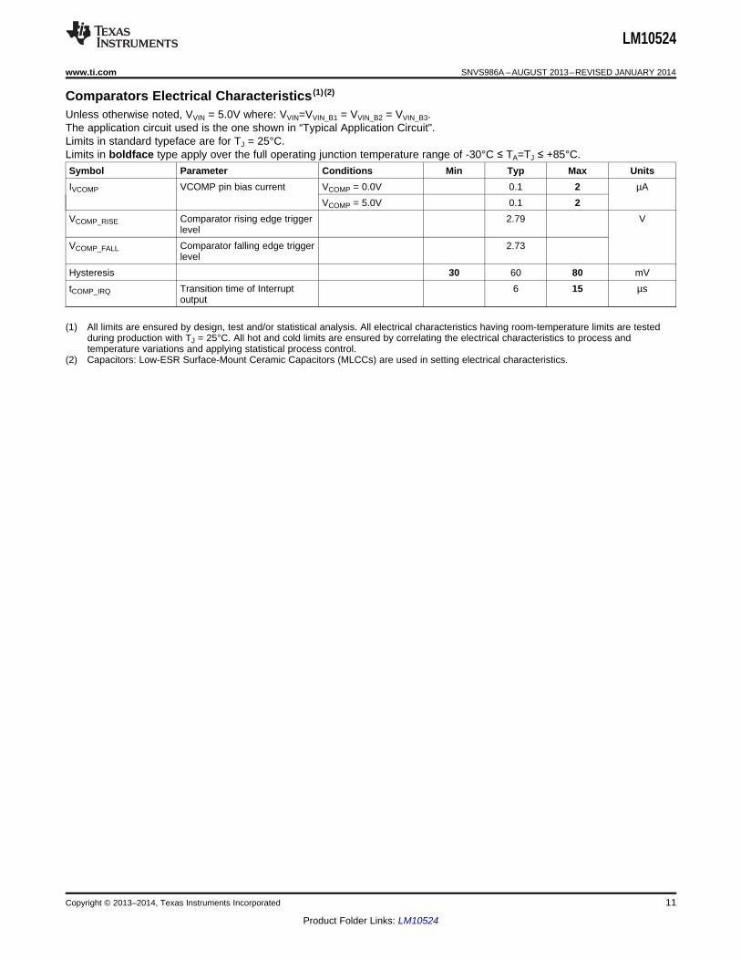
Comparators Electrical Characteristics (1) (2)
Unless otherwise noted, VVIN = 5.0V where: VVIN=VVIN_B1 = VVIN_B2 = VVIN_B3.The application circuit used is the one shown in “Typical Application Circuit".Limits in standard typeface are for TJ = 25°C.Limits in boldface type apply over the full operating junction temperature range of -30°C ≤ TA=TJ ≤ +85°C.Symbol Parameter Conditions Min Typ Max UnitsIVCOMP VCOMP pin bias current VCOMP = 0.0V 0.1 2 µA
VCOMP = 5.0V 0.1 2VCOMP_RISE Comparator rising edge trigger 2.79 V
levelVCOMP_FALL Comparator falling edge trigger 2.73
levelHysteresis 30 60 80 mVtCOMP_IRQ Transition time of Interrupt 6 15 µs
output
(1) All limits are ensured by design, test and/or statistical analysis. All electrical characteristics having room-temperature limits are testedduring production with TJ = 25°C. All hot and cold limits are ensured by correlating the electrical characteristics to process andtemperature variations and applying statistical process control.
(2) Capacitors: Low-ESR Surface-Mount Ceramic Capacitors (MLCCs) are used in setting electrical characteristics.
Copyright © 2013–2014, Texas Instruments Incorporated 11
Product Folder Links: LM10524

0
1
2
3
4
5
6
Out
put
Vol
tage
(V
)
Time (2ms/DIV)
Buck 1Buck 2Buck 3POK
C002
Vol
tage
(1V
/DIV
)
Time (5ms/DIV)
Buck 3Buck 2SLPENDEVSLP
C003
0
10
20
30
40
50
60
70
80
90
100
0.0 0.2 0.4 0.6 0.8 1.0 1.2 1.4 1.6 1.8 2.0 2.2 2.4 2.6
Effi
cien
cy (
%)
Load Current (A)
VIN=3.3V
VIN=4.2V
VIN=5.0V
C006
0.0
0.5
1.0
1.5
2.0
2.5
3.0
3.5
4.0
Out
put
Vol
tage
(V
)
Time (2ms/DIV)
Buck 1Buck 2Buck 3POK
C001
0
10
20
30
40
50
60
70
80
90
100
0.0 0.2 0.4 0.6 0.8 1.0 1.2 1.4 1.6
Effi
cien
cy (
%)
Load Current (A)
VIN=3.7V
VIN=4.2V
VIN=5.0V
C004
0
10
20
30
40
50
60
70
80
90
100
0.0 0.1 0.2 0.3 0.4 0.5 0.6 0.7 0.8 0.9 1.0
Effi
cien
cy (
%)
Load Current (A)
VIN=3.3V
VIN=4.2V
VIN=5.0V
C005
LM10524
SNVS986A –AUGUST 2013–REVISED JANUARY 2014 www.ti.com
Typical Performance Characteristics(All plots are representative typical plots) Vin=5.0V
Buck 1 Efficiency Buck 2 Efficiency
Figure 2. Figure 3.
Buck 3 Efficiency Startup
Figure 4. Figure 5.
POK at DEVSLP DEVSLP Timing 5ms
Figure 6. Figure 7.
12 Copyright © 2013–2014, Texas Instruments Incorporated
Product Folder Links: LM10524

Vol
tage
(1V
/DIV
)
Time (5ms/DIV)
Buck 3Buck 2SLPENDEVSLP
C004
LM10524
www.ti.com SNVS986A –AUGUST 2013–REVISED JANUARY 2014
Typical Performance Characteristics (continued)DEVSLP Timing 10ms Buck 1 - 0 to 750mA
Figure 8. Figure 9.
Buck 1 - 750mA to 1.6A Buck 2 - 0 to 500mA
Figure 10. Figure 11.
Buck 2 - 500 to 1A Buck 3 - 0 to 1.25A
Figure 12. Figure 13.
Copyright © 2013–2014, Texas Instruments Incorporated 13
Product Folder Links: LM10524

LM10524
SNVS986A –AUGUST 2013–REVISED JANUARY 2014 www.ti.com
Typical Performance Characteristics (continued)Buck 3 - 1.25 to 2.5A
Figure 14.
14 Copyright © 2013–2014, Texas Instruments Incorporated
Product Folder Links: LM10524

EN
COMPARATOR
BUCK 2
SPI
OVLOUVLO
SE
QU
EN
CE
R
REGISTERSGND_B2
FB_B2
SW_B2
VIN_B2
GN
D
GN
D
SP
I_C
LK
VIN
_IO
SP
I_D
O
SP
I_D
I
SP
I_C
S
BUCK 1EN
FB_B1
GND_B1
SW_B1
VIN_B1
EN
BUCK 3 GND_B3
FB_B3
SW_B3
VIN_B3
TSD
VCOMP
IRQ
PowerUp_Mode
DEVSLP
GN
D
CONTROLLOGIC
LM10524
DEVSLP_CTRL
DEVSLP_OVR1
DEVSLP_OVR2
SLEEP_ENPWR_OK
LM10524
www.ti.com SNVS986A –AUGUST 2013–REVISED JANUARY 2014
APPLICATION INFORMATIONLM10524 is a highly efficient and integrated Power Management Unit for Systems-on-a-Chip (SoCs), ASICs, andprocessors. It operates cooperatively and communicates with processors over an SPI interface with outputVoltage programmability.
The device incorporates three high-efficiency synchronous buck regulators that deliver three output voltages froma single power source.
The device also includes a SPI programmable Comparator Block that provides an interrupt output signal. Thedevice has a separate logic supply input.
Figure 15. Internal Block Diagram of the LM10524 PMIC
SPI Data InterfaceThe device is programmable via 4-wire SPI Interface. The signals associated with this interface are CS, DI, DOand CLK. Through this interface, the user can enable/disable the device, program the output voltages of theindividual Bucks and of course read the status of Flag registers.
By accessing the registers in the device through this interface, the user can get access and control the operationof the buck controllers and program the reference voltage of the comparator in the device.
Copyright © 2013–2014, Texas Instruments Incorporated 15
Product Folder Links: LM10524

LM10524
SNVS986A –AUGUST 2013–REVISED JANUARY 2014 www.ti.com
Figure 16. SPI Interface Write
• Data Out (DO)• Data In (DI)– All Os– 1 to 0 Write Command
– A4to A0 Register address to be written– D7 to D0 Data to be written
Figure 17. SPI Interface Read
• Data Out (DO)• Data In (DI)– D7 to D0 Data Read– 1 to 1 Read Command
– A4to A0 Register address to be read– Don’t care after A0
16 Copyright © 2013–2014, Texas Instruments Incorporated
Product Folder Links: LM10524
LM10524
www.ti.com SNVS986A –AUGUST 2013–REVISED JANUARY 2014
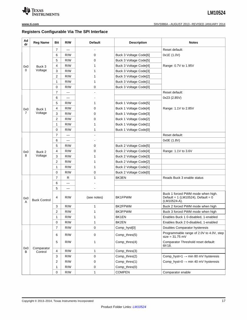
Registers Configurable Via The SPI Interface
Ad Reg Name Bit R/W Default Description Notesdr7 — - Reset default:6 R/W 0 Buck 3 Voltage Code[6] 0x1E (1.0V)5 R/W 0 Buck 3 Voltage Code[5]4 R/W 1 Buck 3 Voltage Code[4] Range: 0.7V to 1.95V0x0 Buck 3
0 Voltage 3 R/W 1 Buck 3 Voltage Code[3]2 R/W 1 Buck 3 Voltage Code[2]1 R/W 1 Buck 3 Voltage Code[1]0 R/W 0 Buck 3 Voltage Code[0]7 — - Reset default:6 — - 0x23 (2.85V)5 R/W 1 Buck 1 Voltage Code[5]4 R/W 0 Buck 1 Voltage Code[4] Range: 1.1V to 2.85V0x0 Buck 1
7 Voltage 3 R/W 0 Buck 1 Voltage Code[3]2 R/W 0 Buck 1 Voltage Code[2]1 R/W 1 Buck 1 Voltage Code[1]0 R/W 1 Buck 1 Voltage Code[0]7 — - Reset default:6 — - 0x0E (1.8V)5 R/W 0 Buck 2 Voltage Code[5]4 R/W 0 Buck 2 Voltage Code[4] Range: 1.1V to 3.6V0x0 Buck 2
8 Voltage 3 R/W 1 Buck 2 Voltage Code[3]2 R/W 1 Buck 2 Voltage Code[2]1 R/W 1 Buck 2 Voltage Code[1]0 R/W 0 Buck 2 Voltage Code[0]7 R 1 BK3EN Reads Buck 3 enable status6 — -5 — -
Buck 1 forced PWM mode when high.4 R/W (see notes) BK1FPWM Default = 1 (LM10524), Default = 00x0 Buck Control (LM10524-A).A3 R/W 1 BK2FPWM Buck 2 forced PWM mode when high2 R/W 1 BK3FPWM Buck 3 forced PWM mode when high1 R/W 1 BK1EN Enables Buck 1 0-disabled, 1-enabled0 R/W 1 BK2EN Enables Buck 2 0-disabled, 1-enabled7 R/W 0 Comp_hyst[0] Doubles Comparator hysteresis
Programmable range of 2.0V to 4.0V, step6 R/W 0 Comp_thres(5) size = 31.75 mV5 R/W 1 Comp_thres(4) Comparator Threshold reset default:
6h'18.0x0 Comparator
4 R/W 1 Comp_thres(3)B Control3 R/W 0 Comp_thres(2) Comp_hyst=1 → min 80 mV hysteresis2 R/W 0 Comp_thres(1) Comp_hyst=0 → min 40 mV hysteresis1 R/W 0 Comp_thres(0)0 R/W 1 COMPEN Comparator enable
Copyright © 2013–2014, Texas Instruments Incorporated 17
Product Folder Links: LM10524

LM10524
SNVS986A –AUGUST 2013–REVISED JANUARY 2014 www.ti.com
Ad Reg Name Bit R/W Default Description Notesdr7 —6 —5 —4 —0x0 Interrupt
C Enable 3 R/W 0 Buck 3 OK2 R/W 0 Buck 2 OK1 R/W 0 Buck 1 OK0 R/W 1 Comparator Interrupt comp event7 —6 —5 —4 R0x0 Interrupt
D Status 3 R Buck 3 OK Buck 3 is greater than 90% of target2 R Buck 2 OK Buck 2 is greater than 90% of target1 R Buck 1 OK Buck 1 is greater than 90% of target0 R Comparator Comparator output is high7 —6 —5 —4 —
0x0 MISC Control 3 —E2 —1 —
Interrupt_polarity=0→Active low Interrupt0 R/W 0 Interrupt Polarity Interrupt_polarity=1→Active high Interrupt
18 Copyright © 2013–2014, Texas Instruments Incorporated
Product Folder Links: LM10524

LM10524
www.ti.com SNVS986A –AUGUST 2013–REVISED JANUARY 2014
ADDR 0x07& 0x08: Buck 1 and Buck 2 Voltage Code and VOUT Level Mapping
Voltage code Voltage Voltage code Voltage0x00 1.10 0x20 2.700x01 1.15 0x21 2.750x02 1.20 0x22 2.800x03 1.25 0x23 2.850x04 1.30 0x24 2.900x05 1.35 0x25 2.950x06 1.40 0x26 3.000x07 1.45 0x27 3.050x08 1.50 0x28 3.100x09 1.55 0x29 3.150x0A 1.60 0x2A 3.200x0B 1.65 0x2B 3.250x0C 1.70 0x2C 3.300x0D 1.75 0x2D 3.350x0E 1.80 0x2E 3.400x0F 1.85 0x2F 3.450x10 1.90 0x30 3.500x11 1.95 0x31 3.550x12 2.00 0x32 3.600x13 2.05 0x33 3.600x14 2.10 0x34 3.600x15 2.15 0x35 3.600x16 2.20 0x36 3.600x17 2.25 0x37 3.600x18 2.30 0x38 3.600x19 2.35 0x39 3.600x1A 2.40 0x3A 3.600x1B 2.45 0x3B 3.600x1C 2.50 0x3C 3.600x1D 2.55 0x3D 3.600x1E 2.60 0x3E 3.600x1F 2.65 0x3F 3.60
Copyright © 2013–2014, Texas Instruments Incorporated 19
Product Folder Links: LM10524

LM10524
SNVS986A –AUGUST 2013–REVISED JANUARY 2014 www.ti.com
ADDR 0x00 & 0x09: Buck 3 Voltage Code and VOUT Level Mapping
Voltage Code Voltage Voltage Code Voltage Voltage Code Voltage Voltage Code Voltage0x00 0.70 0x20 1.02 0x40 1.34 0x60 1.660x01 0.71 0x21 1.03 0x41 1.35 0x61 1.670x02 0.72 0x22 1.04 0x42 1.36 0x62 1.680x03 0.73 0x23 1.05 0x43 1.37 0x63 1.690x04 0.74 0x24 1.06 0x44 1.38 0x64 1.700x05 0.75 0x25 1.07 0x45 1.39 0x65 1.710x06 0.76 0x26 1.08 0x46 1.40 0x66 1.720x07 0.77 0x27 1.09 0x47 1.41 0x67 1.730x08 0.78 0x28 1.10 0x48 1.42 0x68 1.740x09 0.79 0x29 1.11 0x49 1.43 0x69 1.750x0A 0.80 0x2A 1.12 0x4A 1.44 0x6A 1.760x0B 0.81 0x2B 1.13 0x4B 1.45 0x6B 1.770x0C 0.82 0x2C 1.14 0x4C 1.46 0x6C 1.780x0D 0.83 0x2D 1.15 0x4D 1.47 0x6D 1.790x0E 0.84 0x2E 1.16 0x4E 1.48 0x6E 1.800x0F 0.85 0x2F 1.17 0x4F 1.49 0x6F 1.810x10 0.86 0x30 1.18 0x50 1.50 0x70 1.820x11 0.87 0x31 1.19 0x51 1.51 0x71 1.830x12 0.88 0x32 1.20 0x52 1.52 0x72 1.840x13 0.89 0x33 1.21 0x53 1.53 0x73 1.850x14 0.90 0x34 1.22 0x54 1.54 0x74 1.860x15 0.91 0x35 1.23 0x55 1.55 0x75 1.870x16 0.92 0x36 1.24 0x56 1.56 0x76 1.880x17 0.93 0x37 1.25 0x57 1.57 0x77 1.890x18 0.94 0x38 1.26 0x58 1.58 0x78 1.900x19 0.95 0x39 1.27 0x59 1.59 0x79 1.910x1A 0.96 0x3A 1.28 0x5A 1.60 0x7A 1.920x1B 0.97 0x3B 1.29 0x5B 1.61 0x7B 1.930x1C 0.98 0x3C 1.30 0x5C 1.62 0x7C 1.940x1D 0.99 0x3D 1.31 0x5D 1.63 0x7D 1.950x1E 1.00 0x3E 1.32 0x5E 1.640x1F 1.01 0x3F 1.33 0x5F 1.65
20 Copyright © 2013–2014, Texas Instruments Incorporated
Product Folder Links: LM10524

SW
LM10524U1
COUT
CONTROL
PVIN
PGND
FB
CINL
VIN
VO
UT
P
N
S
S
DD
G
G
GND
LM10524
www.ti.com SNVS986A –AUGUST 2013–REVISED JANUARY 2014
ADDR 0x0B: Comparator Threshold Mapping
Voltage code Voltage Voltage code Voltage6h'00 2.000 6h'20 3.0166h'01 2.032 6h'21 3.0486h'02 2.064 6h'22 3.0806h'03 2.095 6h'23 3.1116h'04 2.127 6h'24 3.1436h'05 2.159 6h'25 3.1756h'06 2.191 6h'26 3.2076h'07 2.222 6h'27 3.2386h'08 2.254 6h'28 3.2706h'09 2.286 6h'29 3.3026h'0A 2.318 6h'2A 3.3346h'0B 2.349 6h'2B 3.3656h'0C 2.381 6h'2C 3.3976h'0D 2.413 6h'2D 3.4296h'0E 2.445 6h'2E 3.4616h'0F 2.476 6h'2F 3.4926h'10 2.508 6h'30 3.5246h'11 2.540 6h'31 3.5566h'12 2.572 6h'32 3.5886h'13 2.603 6h'33 3.6196h'14 2.635 6h'34 3.6516h'15 2.667 6h'35 3.6836h'16 2.699 6h'36 3.7156h'17 2.730 6h'37 3.7466h'18 2.762 6h'38 3.7786h'19 2.794 6h'39 3.8106h'1A 2.826 6h'3A 3.8426h'1B 2.857 6h'3B 3.8736h'1C 2.889 6h'3C 3.9056h'1D 2.921 6h'3D 3.9376h'1E 2.953 6h'3E 3.9696h'1F 2.984 6h'3F 4.000
Buck Regulators OperationA buck converter contains a control block, a switching PFET connected between input and output, a synchronousrectifying NFET connected between the output and ground and a feedback path. The figure below shows theblock diagram of each of the three buck regulators integrated in the device.
Figure 18. Buck Functional Diagram
Copyright © 2013–2014, Texas Instruments Incorporated 21
Product Folder Links: LM10524

LM10524
SNVS986A –AUGUST 2013–REVISED JANUARY 2014 www.ti.com
During the first portion of each switching cycle, the control block turns on the internal PFET switch. This allowscurrent to flow from the input through the inductor to the output filter capacitor and load. The inductor limits thecurrent to a ramp with a slope of (VVIN_Bx –VOUT)/L by storing energy in a magnetic field. During the secondportion of each cycle, the control block turns the PFET switch off, blocking current flow from the input, and thenturns the NFET synchronous rectifier on. The inductor draws current from ground through the NFET to the outputfilter capacitor and load, which ramps the inductor current down with a slope of (–VOUT)/L.
The output filter stores charge when the inductor current is high, and releases it when low, smoothing the voltageacross the load. The output voltage is regulated by modulating the PFET switch on time to control the averagecurrent sent to the load. The effect is identical to sending a duty-cycle modulated rectangular wave formed by theswitch and synchronous rectifier at the SW pin to a low-pass filter formed by the inductor and output filtercapacitor. The output voltage is equal to the average voltage at the SW pin.
Buck Regulators DescriptionThe LM10524 incorporates three high efficiency synchronous switching buck regulators that deliver variousvoltages from a single DC input voltage. They include many advanced features to achieve excellent voltageregulation, high efficiency and fast transient response time. The bucks feature voltage mode architecture withsynchronous rectification.
Each of the switching regulators is specially designed for high efficiency operation throughout the load range.With a 2MHz typical switching frequency, the external L-C filter can be small and still provide very low outputvoltage ripple. The bucks are internally compensated to be stable with the recommended external inductors andcapacitors as detailed in the application diagram. Synchronous rectification yields high efficiency for low voltageand high output currents.
All bucks can operate up to a 100% duty cycle allowing for the lowest possible input voltage that still maintainsthe regulation of the output. The lowest input to output dropout voltage is achieved by keeping the PMOS switchon.
Additional features include soft-start, under-voltage lock-out, and current and thermal overload protection. Toreduce the input current ripple, the device employs a control circuit that operates the three bucks at 120° phase.These bucks are nearly identical in performance and mode of operation. They operate in FPWM (forced PWM) orautomatic mode (PWM/PFM).
PWM OperationDuring PWM operation the converter operates as a voltage-mode controller with input voltage feed forward. Thisallows the converter to achieve excellent load and line regulation. The DC gain of the power stage is proportionalto the input voltage. To eliminate this dependence, a feed forward voltage inversely proportional to the inputvoltage is introduced.
In Forced PWM Mode the bucks always operate in PWM mode regardless of the output current.
In Automatic Mode, if the output current is less than 70 mA (typ.), the bucks automatically transition into PFM(Pulse Frequency Modulation) operation to reduce the current consumption. At higher than 100 mA (typ.) theyoperate in PWM mode. This increases the efficiency at lower output currents. The 30 mA (typ.) hysteresis isdesigned in for stable Mode transition.
While in PWM mode, the output voltage is regulated by switching at a constant frequency and then modulatingthe energy per cycle to control power to the load. At the beginning of each clock cycle the PFET switch is turnedon, and the inductor current ramps up until the comparator trips and the control logic turns off the switch. Thecurrent limit comparator can also turn off the switch in case the current limit of the PFET is exceeded. In thiscase the NFET switch is turned on and the inductor current ramps down. The next cycle is initiated by the clockturning off the NFET and turning on the PFET.
22 Copyright © 2013–2014, Texas Instruments Incorporated
Product Folder Links: LM10524

High PFM Threshold
~1.016*Vout
Low1 PFM Threshold
~1.008*Vout
PFM Mode at Light Load
PWM Mode at Moderate to Heavy Loads
PFET onuntil
LPFM limit
reached
NFET ondrains
inductorcurrent
untilI inductor=0
High PFMVoltage
Thresholdreached,go into
Idle mode
Low PFMThreshold,
turn onPFET
Load current increases, draws
Vout towards Low2 PFM Threshold
Low2 PFM Threshold,
switch back to PWM mode
Load current
increases
Low2 PFM Threshold
Vout
Time
Vout
LM10524
www.ti.com SNVS986A –AUGUST 2013–REVISED JANUARY 2014
Figure 19. PFM vs PWM Operation
PFM Operation [BUCK 1, 2 & 3]At very light loads, Buck 1, 2 and Buck 3 enter PFM mode and operate with reduced switching frequency andsupply current to maintain high efficiency.
Buck 1, 2 and 3 will automatically transition into PFM mode when either of two conditions occurs for a duration of32 or more clock cycles:1. The inductor current becomes discontinuous, or2. The peak PMOS switch current drops below the IMODE level.
During PFM operation, the converter positions the output voltage slightly higher than the nominal output voltageduring PWM operation, allowing additional headroom for voltage drop during a load transient from light to heavyload. The PFM comparators sense the output voltage via the feedback pin and control the switching of the outputFETs such that the output voltage ramps between 0.8% and 1.6% (typical) above the nominal PWM outputvoltage. If the output voltage is below the ‘high’ PFM comparator threshold, the PMOS power switch is turned on.It remains on until the output voltage exceeds the ‘high’ PFM threshold or the peak current exceeds the Ipfm levelset for PFM mode.
Once the PMOS power switch is turned off, the NMOS power switch is turned on until the inductor current rampsto zero. When the NMOS zero-current condition is detected, the NMOS power switch is turned off. If the outputvoltage is below the ‘high’ PFM comparator threshold (see Figure 19), the PMOS switch is again turned on andthe cycle is repeated until the output reaches the desired level. Once the output reaches the ‘high’ PFMthreshold, the NMOS switch is turned on briefly to ramp the inductor current to zero and then both outputswitches are turned off and the part enters an extremely low power mode. Quiescent supply current during this‘idle’ mode is less than 100uA, which allows the part to achieve high efficiencies under extremely light loadconditions. When the output drops below the ‘low’ PFM threshold, the cycle repeats to restore the output voltageto ~1.6% above the nominal PWM output voltage.
If the load current should increase during PFM mode causing the output voltage to fall below the ‘low2’ PFMthreshold, the part will automatically transition into fixed-frequency PWM mode.
Soft StartEach of the buck converters has an internal soft-start circuit that limits the in-rush current during start-up. Thisallows the converters to gradually reach the steady state operating point, thus reducing start-up stresses andsurges. During start-up, the switch current limit is increased in steps.
Copyright © 2013–2014, Texas Instruments Incorporated 23
Product Folder Links: LM10524

Ideal Inductor, no resistance
DCR100m Max.
LoadResistance
Load Capacitance
VIN_B1
High Side FET
Model of Inductor
Equivalent Circuit of Bypass Operation of Buck 1
SW_B1 VOUT Buck 1
Bypass FET
FB_B1
LM10524
SNVS986A –AUGUST 2013–REVISED JANUARY 2014 www.ti.com
For Buck 1, 2 and 3 the soft start is implemented by increasing the switch current limit in steps that are graduallygoes higher. The start-up time depends on the output capacitor size, load current and output voltage. Typicalstartup time with the recommended output capacitor of 10uF is 0.1-0.5ms. It is expected that in the finalapplication the load current condition will be more likely in the lower load current range during the start up.
Current LimitingA current limit feature protects the device and any external components during overload conditions. In PWMmode the current limiting is implemented by using an internal comparator that trips at current levels according tothe buck capability. If the output is shorted to ground the device enters a timed current limit mode where theNFET is turned on for a longer duration until the inductor current falls below a low threshold, ensuring inductorcurrent has more time to decay, thereby preventing runaway.
Internal Synchronous RectificationWhile in PWM mode, the bucks use an internal NFET as a synchronous rectifier to reduce the rectifier forwardvoltage drop and the associated power loss. Synchronous rectification provides a significant improvement inefficiency whenever the output voltage is relatively low compared to the voltage drop across an ordinary rectifierdiode.
Bypass-FET Operation on Buck 1This is a factory programmable option, this is disabled on the LM10524 and the LM10524-A.
There is an additional bypass FET used on Buck 1. The FET is connected in parallel to High Side FET andinductor. The bypass threshold will be 3.1V with an option of 3.5V (set by OTP). With standard setting if buck 1input voltage is greater than 3.1V the bypass function is disabled. The determination of whether or not the Buck 1is in bypass mode or standard switching regulation is constantly monitored while the regulator is enabled. If atany time the input voltage goes above 3.1V while in by-pass mode, the regulator will transition to normaloperation.
When the bypass mode is enabled, the output voltage of the buck that is in bypass mode is not regulated, butinstead, the output voltage follows the input voltage minus the voltage drop seen across the FET and DCR of theinductor. The voltage drop is a direct result of the current flowing across those resistive elements. When Buck 1transitions into bypass mode, there is an extra FET used in parallel along with the high side FET for transmissionof the current to the load. This added FET will help reduce the resistance seen by the load and decrease thevoltage drop.
Figure 20. Bypass Operation - Equivalent Circuits
Low Dropout OperationThe device can operate nearly at 100% duty cycle (no switching; PMOS switch completely on) for low drop outsupport. In this way the output voltage will be controlled down to the lowest possible input voltage. When thedevice operates near 100% duty cycle, output voltage ripple is approximately 25 mV.
The minimum input voltage needed to support the output voltage is:VIN_MIN=VOUT+ILOAD*(RDSON_PFET+RIND)
Where:• ILOAD = Load Current
24 Copyright © 2013–2014, Texas Instruments Incorporated
Product Folder Links: LM10524

2.9V
6.05V5.7V
Buck32ms
2msBuck1
2msBuck2
VIN
IRQ
2ms
2ms
VCOMP
2.6V
STARTUP STARTUPUVLO OVLO
2ms
IRQNormal Operation UVLO
15ms
PWR_OK2ms
2ms
3.1V
Byp
ass
If Bypassis Enabled
LM10524
www.ti.com SNVS986A –AUGUST 2013–REVISED JANUARY 2014
• RDSON_PFET = Drain to source resistance of PFET (high side)• RIND = Inductor resistance (1)
Device Operating Modes
Startup SequenceThe startup mode of the LM10524 will depend on the input voltage. Once VIN reaches the UVLO threshold, thereis a 15 msec delay before the LM10524 determines how to set up the buck regulators. If bypass mode is enabledand if VIN is below 3.2V, then Buck 1 will be in bypass mode. See Bypass-FET Operation on Buck 1 forfunctionality description. If the VIN voltage is greater than 3.2V buck 1 will start up as the standard regulators.The 3 buck regulators are staggered during startup to avoid large inrush currents. There is a fixed delay of 2msec between the startup of each regulator.
The Startup Sequence will be:1. 15 msec (±30%) delay after VIN UVLO threshold2. 2 ms delay3. Buck 3 Startup4. 2 ms delay5. Buck 1 Startup6. 2 ms delay7. Buck 2 Startup
Figure 21. Normal Operating Modes
Power-OnThe device is always enabled, unless outside of operating voltage range. There is no LM10524 Enable Pin. OnceVIN reaches a minimum required input Voltage, the power-up sequence will be started automatically and thestartup sequence will be initiated. Once the device is started, the output voltage of the Bucks 1 and 2 can beindividually disabled by accessing their corresponding BKEN register bits (BUCK CONTROL).
Copyright © 2013–2014, Texas Instruments Incorporated 25
Product Folder Links: LM10524

POWERUP_MODE
DEVSLP
DEVSLP_CTRL
DEVSLP_OVR1
DEVSLP_OVR2
SLEEP_EN
OUTPUTS FROM PMIC
VIN
t150mst
Initialisation period for DevSLP circuitStart up period.All signals low or
tri-state.
Sleep mode is available after this edge
LM10524
SNVS986A –AUGUST 2013–REVISED JANUARY 2014 www.ti.com
Sleep FunctionThe Device can be put into Sleep mode where all the outputs and the internal oscillator are switched off. Sleepmode is initiated by the DevSLP pin going high and the function is gated by the state of device pinsDevSLP_OVR1, DevSLP_OVR2, and PowerUp_Enable. DevSLP_CTRL and SLEEP_EN pins are used toindicate the status of the device while DevSLP pin is high.
Device Power UpDuring the device power up there is a 150ms period where all outputs will be low or tri-state. Following this thePowerUp_Mode output will be high and SLEEP_EN output will be low. The DEVSLP_CTRL output will mirror thestate of the DEVSLP input. This initialization phase is complete when the PowerUp_Mode pin is externally pulledlow and the device latches this low state on the pin.
Normal OperationWhen Sleep mode is initiated by the DEVSLP pin being pulled high, this is mirrored to the DEVSLP_CTRL pin.The conditions for entry into Sleep mode are checked, DEVSLP_OVR1, DEVSLP_OVR2, and PowerUp_Modepins must be low. If these conditions are met the Ouput shutdown is started and the DEVSLP_CTRL pin is drivenlow. The SLEEP_EN pin is driven high to indicate that Sleep mode is active. SLEEP_EN will remain high until alloutputs have discharged to zero and DEVSLP goes low. In the case where the DEVSLP input goes low prior tofull discharge, SLEEP_EN will remain high until all outputs have discharged. If any of the gating pinsDEVSLP_OVR1, DEVSLP_OVR2, and PowerUp_Mode go high while in sleep mode SLEEP_EN will go low andDEVSLP_CTRL will go to the same state as DEVSLP pin.
19.2.3 DEVSLP TimingInitialization phase:
Figure 22. Initialization
26 Copyright © 2013–2014, Texas Instruments Incorporated
Product Folder Links: LM10524

POWERUP_MODE
DEVSLP
DEVSLP_CTRL
DEVSLP_OVR1
DEVSLP_OVR2
SLEEP_EN
OUTPUTS FROM PMIC
VIN
t25mst
150ms
2µs
150ms
LM10524
www.ti.com SNVS986A –AUGUST 2013–REVISED JANUARY 2014
After device power up the regulated outputs are on and at their specified outputs voltages indicated by the‘Outputs from PMIC’ trace above. All DEVSLP signals are low or tri-state for a period of 150ms. Following this150ms period the device will hold SLEEP_EN low and will allow the POWERUP_MODE pin to go high via a 1KΩpullup resistor referenced to VIN supply. The DEVSLP function is ready when the POWERUP_MODE pin ispulled low externally, This negative edge on the POWERUP_MODE pin triggers the device to pulldown thePOWERUP_MODE pin and this output remains low until a device reset. During this Initialization phase theDEVSLP_CTRL output mirrors the input at DEVSLP. The two signals DEVSLP_OVR1/2 are ignored by thedevice during this phase.
Normal Operation, DEVSLP high period > Outputs discharge time:
Figure 23. DEVSLP, Period Greater than Output Discharge Time
In normal operation when DEVSLP goes high, DEVSLP_CNTL will go high. The device checks the status ofDEVSLP_OVR1 and DEVSLP_OVR2 as well as POWERUP_MODE to ensure they are low to allow entry intoSLEEP mode. If these conditions are met then the device will power down all outputs in their time sequence andthe DEVSLP_CTRL pin is forced low. SLEEP_EN is forced high. Following the outputs discharging to zeroDEVSLP goes low, SLEEP_EN is driven low and the regulated outputs switch on in their determined timesequence.
Normal Operation, DEVSLP high period < Outputs discharge time
Copyright © 2013–2014, Texas Instruments Incorporated 27
Product Folder Links: LM10524

POWERUP_MODE
DEVSLP
DEVSLP_CTRL
DEVSLP_OVR1
DEVSLP_OVR2
SLEEP_EN
OUTPUTS FROM PMIC
VIN
t14mst
*4ms + 10ms min sleep slot time
* Time set by OTP
150ms
t10mst
2µs
150ms
LM10524
SNVS986A –AUGUST 2013–REVISED JANUARY 2014 www.ti.com
Figure 24. DEVSLP. Period less than Output Discharge Time
As above; in normal operation when DEVSLP goes high DEVSLP_CNTL will go high. The device checks thestatus of DEVSLP_OVR1 and DEVSLP_OVR2 as well as POWERUP_MODE to ensure they are low to allowentry into SLEEP mode. If these conditions are met then the device will power down all outputs in their timesequence (4ms) and the DEVSLP_CTRL pin is forced low. SLEEP_EN is forced high. In this case DEVSLP goeshigh prior to full output discharge to zero. SLEEP_EN will be forced low after a set time, (programmable) withdefault set to10ms (+4ms) to ensure the device outputs discharge fully. This timing is important to ensure properdischarge of the output capacitance (up to 100µF in a 7.5ms period. The device outputs will also be switched onafter this time period. To ensure all buck outputs are discharged a minimum sleep time exists, this time isconfigured to 12ms (programmable set by OTP).In the case where DEVSLP is active for, <12ms, the SLEEP_ENand sleep cycle will be held for a minimum of 12ms.
28 Copyright © 2013–2014, Texas Instruments Incorporated
Product Folder Links: LM10524
Buck3
Buck1
Buck2
VIN
2ms
2ms
STARTUP
15 ms
2ms
Normal Operation
POWER UP_MODE
DEVSLP
DEVSLP_CTRL
DEVSLP_OVR2
DEVSLP_OVR1
SLEEP
SLEEP_EN
POK
LM10524
www.ti.com SNVS986A –AUGUST 2013–REVISED JANUARY 2014
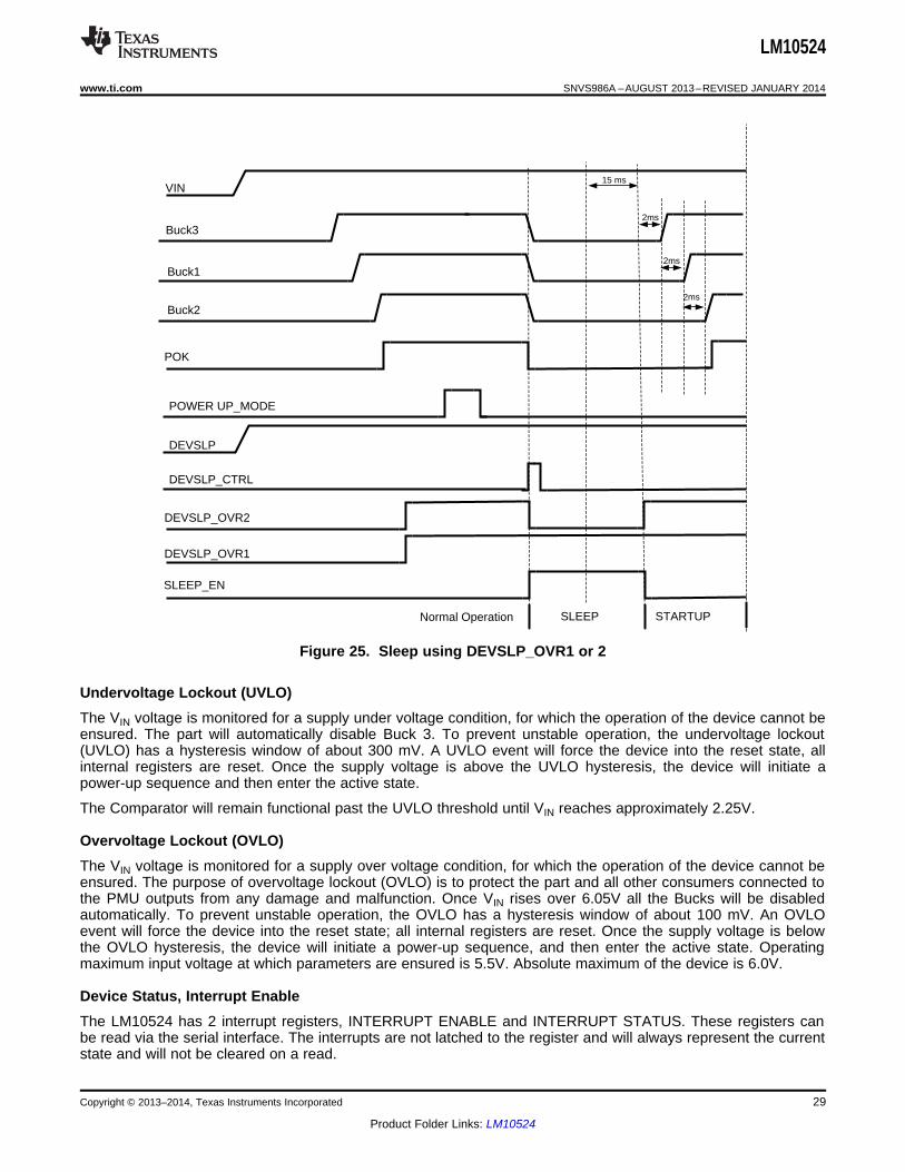
Figure 25. Sleep using DEVSLP_OVR1 or 2
Undervoltage Lockout (UVLO)The VIN voltage is monitored for a supply under voltage condition, for which the operation of the device cannot beensured. The part will automatically disable Buck 3. To prevent unstable operation, the undervoltage lockout(UVLO) has a hysteresis window of about 300 mV. A UVLO event will force the device into the reset state, allinternal registers are reset. Once the supply voltage is above the UVLO hysteresis, the device will initiate apower-up sequence and then enter the active state.
The Comparator will remain functional past the UVLO threshold until VIN reaches approximately 2.25V.
Overvoltage Lockout (OVLO)The VIN voltage is monitored for a supply over voltage condition, for which the operation of the device cannot beensured. The purpose of overvoltage lockout (OVLO) is to protect the part and all other consumers connected tothe PMU outputs from any damage and malfunction. Once VIN rises over 6.05V all the Bucks will be disabledautomatically. To prevent unstable operation, the OVLO has a hysteresis window of about 100 mV. An OVLOevent will force the device into the reset state; all internal registers are reset. Once the supply voltage is belowthe OVLO hysteresis, the device will initiate a power-up sequence, and then enter the active state. Operatingmaximum input voltage at which parameters are ensured is 5.5V. Absolute maximum of the device is 6.0V.
Device Status, Interrupt EnableThe LM10524 has 2 interrupt registers, INTERRUPT ENABLE and INTERRUPT STATUS. These registers canbe read via the serial interface. The interrupts are not latched to the register and will always represent the currentstate and will not be cleared on a read.
Copyright © 2013–2014, Texas Instruments Incorporated 29
Product Folder Links: LM10524

LM10524
SNVS986A –AUGUST 2013–REVISED JANUARY 2014 www.ti.com
If interrupt condition is detected, then corresponding bit in the INTERRUPT STATUS register (0x0D) is set to '1',and Interrupt output is asserted. There are 5 interrupt generating conditions:• Buck 3 output is over flag level (90% when rising, 85% when falling)• Buck 2 output is over flag level (90% when rising, 85% when falling)• Buck 1 output is over flag level (90% when rising, 85% when falling)• Comparator input voltage crosses over selected threshold
Reading the interrupt register will not release Interrupt output. Interrupt generation conditions can be individuallyenabled or disabled by writing respective bits in INTERRUPT ENABLE register (0x0C) to '1' or '0'.
Thermal Shutdown (TSD)The temperature of the silicon die is monitored for an over-temperature condition, for which the operation of thedevice can not be ensured. The part will automatically be disabled if the temperature is too high (>140°C). Thethermal shutdown (TSD) will force the device into the reset state. In reset, all circuitry is disabled. To preventunstable operation, the TSD has a hysteresis window of about 20°C. Once the temperature has decreased belowthe TSD hysteresis, the device will initiate a powerup sequence and then enter the active state. In the activestate, the part will start up as if for the first time, all registers will be in their default state.
ComparatorThe comparator on the LM10524 takes its inputs from the VCOMP pin and an internal threshold level which isprogrammed by the user. The threshold level is programmable between 2.0 and 4.0V with a step of 31 mV and adefault comp code of 6h'18. The output of the comparator is the Interrupt pin. Its polarity can be changed usingRegister 0x0E bit 0. If Interrupt polarity = 0 → Active low (default) is selected, then the output is low if VCOMPvalue is greater than the threshold level. The output is high if the VCOMP value is less than the threshold level. IfInterrupt polarity = 1 → Active high is selected then the output is high if VCOMP value is greater than the thresholdlevel. The output is low if the VCOMP value is less than the threshold level. There is some hysteresis when VCOMPtransitions from high to low, typically 60 mV. There is a control bit in register 0x0B, comparator control, that candouble the hysteresis value.
Figure 26. Comparator Thresholds
Thermal Shutdown (TSD)The temperature of the silicon die is monitored for an over-temperature condition, for which the operation of thedevice cannot be ensured. The part will automatically be disabled if the temperature is too high. The thermalshutdown (TSD) will force the device into the reset state. In reset, all circuitry is disabled. To prevent unstableoperation, the TSD has a hysteresis window of about 20°C. Once the temperature has decreased below the TSDhysteresis, the device will initiate a power-up sequence and then enter the active state. In the active state, thepart will start up as if for the first time, all registers will be in their default state.
External Components SelectionAll three switchers require an input capacitor and an output inductor-capacitor filter. These components arecritical to the performance of the device. All three switchers are internally compensated and do not requireexternal components to achieve stable operation. The output voltages of the bucks can be programmed throughthe SPI pins.
30 Copyright © 2013–2014, Texas Instruments Incorporated
Product Folder Links: LM10524

SAT PEAK
RIPPLEPEAK OUTMAX
IN OUTRIPPLE
S
OUT
IN
I IL
IIL I
2D (V V )
IL F
VD
V EFF
!
u
u
u
L(MAX) LOAD(MAX) RIPPLE
IN OUTLOAD(MAX)
S
IN OUTLOAD(MAX)
OUTS
IN
I I I
D (V V )I
2 L F
D (V V )I (A typ.),
2 2.2 2.0V
D , F 2 MHz, L 2.2 HV
'
u
u u
u |
u u
P
LM10524
www.ti.com SNVS986A –AUGUST 2013–REVISED JANUARY 2014
Output Inductors & Capacitors SelectionThere are several design considerations related to the selection of output inductors and capacitors:• Load transient response• Stability• Efficiency• Output ripple voltage• Over current ruggedness
The device has been optimized for use with nominal LC values as shown in the Typical Application Circuit.
Inductor SelectionThe recommended inductor values are shown in Typical Application Diagram. It is important to ensure theinductor core does not saturate during any foreseeable operational situation. The inductor should be rated tohandle the peak load current plus the ripple current.
Care should be taken when reviewing the different saturation current ratings that are specified by differentmanufacturers. Saturation current ratings are typically specified at 25°C, so ratings at maximum ambienttemperature of the application should be requested from the manufacturer.
(2)
There are two methods to choose the inductor saturation current rating:
Recommended Method for Inductor Selection:The best way to ensure the inductor does not saturate is to choose an inductor that has saturation current ratinggreater than the maximum device current limit, as specified in the Electrical Characteristics tables. In this casethe device will prevent inductor saturation by going into current limit before the saturation level is reached.
Alternate Method for Inductor Selection:If the recommended approach cannot be used care must be taken to ensure that the saturation current is greaterthan the peak inductor current:
Where:• ISAT: Inductor saturation current at operating temperature• ILPEAK: Peak inductor current during worst case conditions• IOUTMAX: Maximum average inductor current• IRIPPLE: Peak-to-Peak inductor current• VOUT: Output voltage
Copyright © 2013–2014, Texas Instruments Incorporated 31
Product Folder Links: LM10524

LM10524
SNVS986A –AUGUST 2013–REVISED JANUARY 2014 www.ti.com
• VIN: Input voltage• L: Inductor value in Henries at IOUTMAX
• F: Switching frequency, Hertz• D: Estimated duty factor• EFF: Estimated power supply efficiency (3)
ISAT may not be exceeded during any operation, including transients, startup, high temperature, worst-caseconditions, etc.
Suggested Inductors and Their SuppliersThe designer should choose the inductors that best match the system requirements. A very wide range ofinductors are available as regarding physical size, height, maximum current (thermally limited, and inductanceloss limited), series resistance, maximum operating frequency, losses, etc. In general, smaller physical sizeinductors will have higher series resistance (DCR) and implicitly lower overall efficiency is achieved. Very low-profile inductors may have even higher series resistance. The designer should try to find the best compromisebetween system performance and cost.
Value Manufacturer Part Number DCR Current Package1.0 µH Murata LQH44PN1R0NP0 30 mΩ 2.95A 16161.0 µH Murata LQH32PN1R0NNC 45mΩ 2.5A 3225(1210)1.0 µH Coilcraft XFL3012-102MEC 35 mΩ 2.5A 30121.0 µH Coilcraft LPS4012-102NL 70mΩ 3.0A 40122.2 µH Coilcraft XFL3012-222MEC 81 mΩ 1.6A 30122.2 µH Murata LQH55PN2R2NR0L 31 mΩ 2.5A 2220
Output and Input Capacitors CharacteristicsSpecial attention should be paid when selecting these components. As shown in the following figure, the DC biasof these capacitors can result in a capacitance value that falls below the minimum value given in therecommended capacitor specifications table. Note that the graph shows the capacitance out of spec for the 0402case size capacitor at higher bias voltages. It is therefore recommended that the capacitor manufacturers’specifications for the nominal value capacitor are consulted for all conditions, as some capacitor sizes (e.g.0402)may not be suitable in the actual application.
Figure 27. Typical Variation in Capacitance vs.DC Bias
32 Copyright © 2013–2014, Texas Instruments Incorporated
Product Folder Links: LM10524
RIPPLEROUT RIPPLE COUT COUT
S OUT
IV I ESR and V
8 F C u
u u
2 2OUT RIPPLE PP ROUT COUTV V V
IN OUT OUTRIPPLEOUT RIPPLE PP RIPPLE
S OUT S IN
D (V V ) VIV where I and D
8 F C 2 L F V
u ' '
u u u u
LM10524
www.ti.com SNVS986A –AUGUST 2013–REVISED JANUARY 2014
The ceramic capacitor’s capacitance can vary with temperature. The capacitor type X7R, which operates over atemperature range of −55°C to +125°C, will only vary the capacitance to within ±15%. The capacitor type X5Rhas a similar tolerance over a reduced temperature range of −55°C to +85°C. Many large value ceramiccapacitors, larger than 1µF are manufactured with Z5U or Y5V temperature characteristics. Their capacitancecan drop by more than 50% as the temperature varies from 25°C to 85°C. Therefore X7R is recommended overZ5U and Y5V in applications where the ambient temperature will change significantly above or below 25°C.
Tantalum capacitors are less desirable than ceramic for use as output capacitors because they are moreexpensive when comparing equivalent capacitance and voltage ratings in the 0.47µF to 44µF range. Anotherimportant consideration is that tantalum capacitors have higher ESR values than equivalent size ceramics. Thismeans that while it may be possible to find a tantalum capacitor with an ESR value within the stable range, itwould have to be larger in capacitance (which means bigger and more costly) than a ceramic capacitor with thesame ESR value. It should also be noted that the ESR of a typical tantalum will increase about 2:1 as thetemperature goes from 25°C down to −30°C, so some guard band must be allowed.
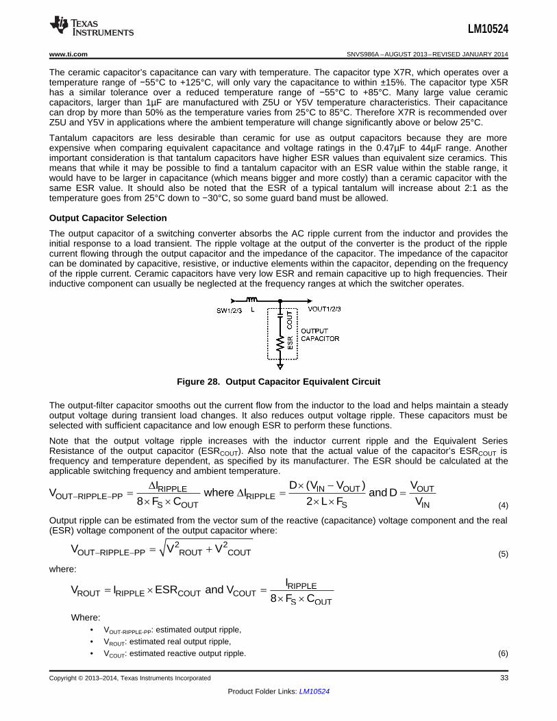
Output Capacitor SelectionThe output capacitor of a switching converter absorbs the AC ripple current from the inductor and provides theinitial response to a load transient. The ripple voltage at the output of the converter is the product of the ripplecurrent flowing through the output capacitor and the impedance of the capacitor. The impedance of the capacitorcan be dominated by capacitive, resistive, or inductive elements within the capacitor, depending on the frequencyof the ripple current. Ceramic capacitors have very low ESR and remain capacitive up to high frequencies. Theirinductive component can usually be neglected at the frequency ranges at which the switcher operates.
Figure 28. Output Capacitor Equivalent Circuit
The output-filter capacitor smooths out the current flow from the inductor to the load and helps maintain a steadyoutput voltage during transient load changes. It also reduces output voltage ripple. These capacitors must beselected with sufficient capacitance and low enough ESR to perform these functions.
Note that the output voltage ripple increases with the inductor current ripple and the Equivalent SeriesResistance of the output capacitor (ESRCOUT). Also note that the actual value of the capacitor’s ESRCOUT isfrequency and temperature dependent, as specified by its manufacturer. The ESR should be calculated at theapplicable switching frequency and ambient temperature.
(4)
Output ripple can be estimated from the vector sum of the reactive (capacitance) voltage component and the real(ESR) voltage component of the output capacitor where:
(5)
where:
Where:• VOUT-RIPPLE-PP: estimated output ripple,• VROUT: estimated real output ripple,• VCOUT: estimated reactive output ripple. (6)
Copyright © 2013–2014, Texas Instruments Incorporated 33
Product Folder Links: LM10524
OUTPPIN OUT CIN
IN S
I DV I ESR
C F
u u
u
2D _ CIN RMS _ CIN ESR _ CINP I R u
OUT IN OUTRMS _ CIN OUT
IN
V (V V )I I
V
LM10524
SNVS986A –AUGUST 2013–REVISED JANUARY 2014 www.ti.com
The device is designed to be used with ceramic capacitors on the outputs of the buck regulators. Therecommended dielectric type of these capacitors is X5R, X7R, or of comparable material to maintain propertolerances over voltage and temperature. The recommended value for the output capacitors is 22μF, 6.3V withan ESR of 2mΩ or less. The output capacitors need to be mounted as close as possible to the output/groundpins of the device.
Model Vendor Type Vendor Voltage Rating Case SizeGRM155B03J225KE95 Ceramic, X5R Murata 6.3V 603GRM155R60J475ME47 Ceramic, X5R Murata 6.3V 603GRM188B03J226MEA0 Ceramic, X5R Murata 6.3V 603GRM21BB30J476ME15 Ceramic, X5R Murata 6.3V 805
Input Capacitor SelectionThere are 3 buck regulators in the LM10524 device. Each of these buck regulators has its own input capacitorwhich should be located as close as possible to their corresponding SWx_VIN and SWx_GND pins, where xdesignates Buck 1, 2 or 3. The 3 buck regulators operate at 120° out of phase, which means that they switch onat equally spaced intervals, in order to reduce the input power rail ripple. It is recommended to connect all thesupply/ground pins of the buck regulators, SWx_VIN to two solid internal planes located under the device. In thisway, the 3 input capacitors work together and further reduce the input current ripple. A larger tantalum capacitorcan also be located in the proximity of the device.
The input capacitor supplies the AC switching current drawn from the switching action of the internal powerFETs. The in- put current of a buck converter is discontinuous, so the ripple current supplied by the inputcapacitor is large. The input capacitor must be rated to handle both the RMS current and the dissipated power.
The input capacitor must be rated to handle this current:
(7)
The power dissipated in the input capacitor is given by:
(8)
The device is designed to be used with ceramic capacitors on the inputs of the buck regulators. Therecommended dielectric type of these capacitors is X5R, X7R, or of comparable material to maintain propertolerances over voltage and temperature. The minimum recommended value for the input capacitor is 10 µF withan ESR of 10mΩ or less. The input capacitors need to be mounted as close as possible to the power/groundinput pins of the device.
The input power source supplies the average current continuously. During the PFET switch on-time, however,the demanded di/dt is higher than can be typically supplied by the input power source. This delta is supplied bythe input capacitor.
A simplified “worst case” assumption is that all of the PFET current is supplied by the input capacitor. This willresult in conservative estimates of input ripple voltage and capacitor RMS current.
Input ripple voltage is estimated as follows:
where:• VPPIN: estimated peak-to-peak input ripple voltage,• IOUT: output Current• CIN: input capacitor value• ESRCIN: input capacitor ESR. (9)
This capacitor is exposed to significant RMS current, so it is important to select a capacitor with an adequateRMS current rating. Capacitor RMS current estimated as follows:
34 Copyright © 2013–2014, Texas Instruments Incorporated
Product Folder Links: LM10524

LM10524
COUT
CINL
P
N
S
S
D
D
G
G
PGND
VINC
ON
TR
OL
LOOP 1
LOOP 2SW
Vin
22 RIPPLE
RMSCIN OUTI
I D I12
§ · u ¨ ¸
¨ ¸© ¹
LM10524
www.ti.com SNVS986A –AUGUST 2013–REVISED JANUARY 2014
• IRMSCIN: estimated input capacitor RMS current. (10)
PCB Layout ConsiderationsPC board layout is an important part of DC-DC converter design. Poor board layout can disrupt the performanceof a DC- DC converter and surrounding circuitry by contributing to EMI, ground bounce, and resistive voltage lossin the traces. These can send erroneous signals to the DC-DC converter resulting in poor regulation or instability.Good layout can be implemented by following a few simple design rules.
Figure 29. Buck Schematic Showing Layout Sensitive Nodes
1. Minimize area of switched current loops. In a buck regulator there are two loops where currents are switchedrapidly. The first loop starts from the CIN input capacitor, to the regulator Vin pin, through to PGND and backto the CIN input capacitor. The second loop starts from the output capacitor ground, to the regulator PGNDpins, to the inductor and then out to COUT and the load (see Figure 29). To minimize both loop areas theinput capacitor should be placed as close as possible to the PVIN pin. Grounding for both the input andoutput capacitors should consist of a small localized top side plane that connects to PGND. The inductorshould be placed as close as possible to the SW pin and output capacitor.
2. Minimize the copper area of the switch node. The SW pins should be directly connected with a trace thatruns on top side directly to the inductor. To minimize IR losses this trace should be as short as possible andwith a sufficient width. However, a trace that is wider than 100 mils will increase the copper area and causetoo much capacitive loading on the SW pin. The inductors should be placed as close as possible to the SWpins to further minimize the copper area of the switch node.
3. Have a single point ground for all device analog grounds. The ground connections for the feedbackcomponents should be connected together then routed to the GND pin of the device. This prevents anyswitched or load currents from flowing in the analog ground plane. If not properly handled, poor groundingcan result in degraded load regulation or erratic switching behavior.
4. Minimize trace length to the FB pin. The feedback trace should be routed away from the SW pin and inductorto avoid contaminating the feedback signal with switch noise.
5. Make input and output bus connections as wide as possible. This reduces any voltage drops on the input oroutput of the converter and can improve efficiency. If voltage accuracy at the load is important make surefeedback voltage sense is made at the load. Doing so will correct for voltage drops at the load and providethe best output accuracy.
PCB Layout Thermal Dissipation for Micro SMD Package1. Position ground layer as close as possible to micro SMD package. Second PCB layer is usually good option.2. Draw power traces as wide as possible. Bumps which carry high currents should be connected to wide
traces. This helps the silicon to cool down.
Copyright © 2013–2014, Texas Instruments Incorporated 35
Product Folder Links: LM10524
LM10524
SNVS986A –AUGUST 2013–REVISED JANUARY 2014 www.ti.com
REVISION HISTORY
Changes from Original (August 2013) to Revision A Page
• Added Device Information Table .......................................................................................................................................... 6
36 Copyright © 2013–2014, Texas Instruments Incorporated
Product Folder Links: LM10524

PACKAGE OPTION ADDENDUM
www.ti.com 17-May-2018
Addendum-Page 1
PACKAGING INFORMATION
Orderable Device Status(1)
Package Type PackageDrawing
Pins PackageQty
Eco Plan(2)
Lead/Ball Finish(6)
MSL Peak Temp(3)
Op Temp (°C) Device Marking(4/5)
Samples
LM10524TME-A/NOPB NRND DSBGA YFR 46 250 Green (RoHS& no Sb/Br)
SNAGCU Level-1-260C-UNLIM 0 to 0 V089
LM10524TME/NOPB ACTIVE DSBGA YFR 46 250 Green (RoHS& no Sb/Br)
SNAGCU Level-1-260C-UNLIM -30 to 85 V088
LM10524TMX-A/NOPB ACTIVE DSBGA YFR 46 1000 Green (RoHS& no Sb/Br)
SNAGCU Level-1-260C-UNLIM -30 to 85 V089
LM10524TMX/NOPB NRND DSBGA YFR 46 1000 Green (RoHS& no Sb/Br)
SNAGCU Level-1-260C-UNLIM 0 to 0 V088
(1) The marketing status values are defined as follows:ACTIVE: Product device recommended for new designs.LIFEBUY: TI has announced that the device will be discontinued, and a lifetime-buy period is in effect.NRND: Not recommended for new designs. Device is in production to support existing customers, but TI does not recommend using this part in a new design.PREVIEW: Device has been announced but is not in production. Samples may or may not be available.OBSOLETE: TI has discontinued the production of the device.
(2) RoHS: TI defines "RoHS" to mean semiconductor products that are compliant with the current EU RoHS requirements for all 10 RoHS substances, including the requirement that RoHS substancedo not exceed 0.1% by weight in homogeneous materials. Where designed to be soldered at high temperatures, "RoHS" products are suitable for use in specified lead-free processes. TI mayreference these types of products as "Pb-Free".RoHS Exempt: TI defines "RoHS Exempt" to mean products that contain lead but are compliant with EU RoHS pursuant to a specific EU RoHS exemption.Green: TI defines "Green" to mean the content of Chlorine (Cl) and Bromine (Br) based flame retardants meet JS709B low halogen requirements of <=1000ppm threshold. Antimony trioxide basedflame retardants must also meet the <=1000ppm threshold requirement.
(3) MSL, Peak Temp. - The Moisture Sensitivity Level rating according to the JEDEC industry standard classifications, and peak solder temperature.
(4) There may be additional marking, which relates to the logo, the lot trace code information, or the environmental category on the device.
(5) Multiple Device Markings will be inside parentheses. Only one Device Marking contained in parentheses and separated by a "~" will appear on a device. If a line is indented then it is a continuationof the previous line and the two combined represent the entire Device Marking for that device.
(6) Lead/Ball Finish - Orderable Devices may have multiple material finish options. Finish options are separated by a vertical ruled line. Lead/Ball Finish values may wrap to two lines if the finishvalue exceeds the maximum column width.
Important Information and Disclaimer:The information provided on this page represents TI's knowledge and belief as of the date that it is provided. TI bases its knowledge and belief on informationprovided by third parties, and makes no representation or warranty as to the accuracy of such information. Efforts are underway to better integrate information from third parties. TI has taken and

PACKAGE OPTION ADDENDUM
www.ti.com 17-May-2018
Addendum-Page 2
continues to take reasonable steps to provide representative and accurate information but may not have conducted destructive testing or chemical analysis on incoming materials and chemicals.TI and TI suppliers consider certain information to be proprietary, and thus CAS numbers and other limited information may not be available for release.
In no event shall TI's liability arising out of such information exceed the total purchase price of the TI part(s) at issue in this document sold by TI to Customer on an annual basis.

TAPE AND REEL INFORMATION
*All dimensions are nominal
Device PackageType
PackageDrawing
Pins SPQ ReelDiameter
(mm)
ReelWidth
W1 (mm)
A0(mm)
B0(mm)
K0(mm)
P1(mm)
W(mm)
Pin1Quadrant
LM10524TME-A/NOPB DSBGA YFR 46 250 178.0 12.4 3.02 3.42 0.76 8.0 12.0 Q1
LM10524TME/NOPB DSBGA YFR 46 250 178.0 12.4 3.02 3.42 0.76 8.0 12.0 Q1
LM10524TMX-A/NOPB DSBGA YFR 46 1000 178.0 12.4 3.02 3.42 0.76 8.0 12.0 Q1
LM10524TMX/NOPB DSBGA YFR 46 1000 178.0 12.4 3.02 3.42 0.76 8.0 12.0 Q1
PACKAGE MATERIALS INFORMATION
www.ti.com 28-Sep-2017
Pack Materials-Page 1

*All dimensions are nominal
Device Package Type Package Drawing Pins SPQ Length (mm) Width (mm) Height (mm)
LM10524TME-A/NOPB DSBGA YFR 46 250 210.0 185.0 35.0
LM10524TME/NOPB DSBGA YFR 46 250 210.0 185.0 35.0
LM10524TMX-A/NOPB DSBGA YFR 46 1000 210.0 185.0 35.0
LM10524TMX/NOPB DSBGA YFR 46 1000 210.0 185.0 35.0
PACKAGE MATERIALS INFORMATION
www.ti.com 28-Sep-2017
Pack Materials-Page 2

www.ti.com
PACKAGE OUTLINE
C
B E A
D
0.675 MAX
0.2050.165
2.8TYP
2.4 TYP
0.4TYP
0.4 TYP
46X 0.280.25
DSBGA - 0.675 mm max heightYFR0046DIE SIZE BALL GRID ARRAY
4219451/A 06/2014
NOTES: 1. All linear dimensions are in millimeters. Any Dimensions in parenthesis are for reference only. Dimensioning and tolerancing per ASME Y14.5M.2. This drawing is subject to change without notice.
BALL A1CORNER
SEATING PLANEBALL TYP
G
F
E
D
C
1 2 3
0.005 C A B
4 5 6 7
SYMM
SYMM
A
B
H
SCALE 5.000
D: Max =
E: Max =
3.24 mm, Min =
2.84 mm, Min =
3.18 mm
2.78 mm

www.ti.com
EXAMPLE BOARD LAYOUT
46X 0.240.21
(0.4) TYP
(0.4) TYP
( )METAL0.225 0.05 MAX
SOLDER MASKOPENING
METALUNDERMASK
( )SOLDER MASKOPENING
0.225
0.05 MIN
DSBGA - 0.675 mm max heightYFR0046DIE SIZE BALL GRID ARRAY
4219451/A 06/2014
NOTES: (continued) 3. Final dimensions may vary due to manufacturing tolerance considerations and also routing constraints. For more information, see Texas Instruments literature number SBVA017 (www.ti.com/lit/sbva017).
1
SYMM
SYMM
LAND PATTERN EXAMPLESCALE:20X
H
G
F
E
D
C
2 3 4 5 6 7
A
B
NON-SOLDER MASKDEFINED
(PREFERRED)
SOLDER MASK DETAILSNOT TO SCALE
SOLDER MASKDEFINED

www.ti.com
EXAMPLE STENCIL DESIGN
(0.4)TYP
(0.4) TYP
46X ( 0.25) (R ) TYP0.05
METALTYP
DSBGA - 0.675 mm max heightYFR0046DIE SIZE BALL GRID ARRAY
4219451/A 06/2014
NOTES: (continued) 4. Laser cutting apertures with trapezoidal walls and rounded corners may offer better paste release.
H
G
F
E
D
C
1 2 3 4 5 6 7A
B
SYMM
SYMM
SOLDER PASTE EXAMPLEBASED ON 0.1 mm THICK STENCIL
SCALE:20X
IMPORTANT NOTICE
Texas Instruments Incorporated (TI) reserves the right to make corrections, enhancements, improvements and other changes to itssemiconductor products and services per JESD46, latest issue, and to discontinue any product or service per JESD48, latest issue. Buyersshould obtain the latest relevant information before placing orders and should verify that such information is current and complete.TI’s published terms of sale for semiconductor products (http://www.ti.com/sc/docs/stdterms.htm) apply to the sale of packaged integratedcircuit products that TI has qualified and released to market. Additional terms may apply to the use or sale of other types of TI products andservices.Reproduction of significant portions of TI information in TI data sheets is permissible only if reproduction is without alteration and isaccompanied by all associated warranties, conditions, limitations, and notices. TI is not responsible or liable for such reproduceddocumentation. Information of third parties may be subject to additional restrictions. Resale of TI products or services with statementsdifferent from or beyond the parameters stated by TI for that product or service voids all express and any implied warranties for theassociated TI product or service and is an unfair and deceptive business practice. TI is not responsible or liable for any such statements.Buyers and others who are developing systems that incorporate TI products (collectively, “Designers”) understand and agree that Designersremain responsible for using their independent analysis, evaluation and judgment in designing their applications and that Designers havefull and exclusive responsibility to assure the safety of Designers' applications and compliance of their applications (and of all TI productsused in or for Designers’ applications) with all applicable regulations, laws and other applicable requirements. Designer represents that, withrespect to their applications, Designer has all the necessary expertise to create and implement safeguards that (1) anticipate dangerousconsequences of failures, (2) monitor failures and their consequences, and (3) lessen the likelihood of failures that might cause harm andtake appropriate actions. Designer agrees that prior to using or distributing any applications that include TI products, Designer willthoroughly test such applications and the functionality of such TI products as used in such applications.TI’s provision of technical, application or other design advice, quality characterization, reliability data or other services or information,including, but not limited to, reference designs and materials relating to evaluation modules, (collectively, “TI Resources”) are intended toassist designers who are developing applications that incorporate TI products; by downloading, accessing or using TI Resources in anyway, Designer (individually or, if Designer is acting on behalf of a company, Designer’s company) agrees to use any particular TI Resourcesolely for this purpose and subject to the terms of this Notice.TI’s provision of TI Resources does not expand or otherwise alter TI’s applicable published warranties or warranty disclaimers for TIproducts, and no additional obligations or liabilities arise from TI providing such TI Resources. TI reserves the right to make corrections,enhancements, improvements and other changes to its TI Resources. TI has not conducted any testing other than that specificallydescribed in the published documentation for a particular TI Resource.Designer is authorized to use, copy and modify any individual TI Resource only in connection with the development of applications thatinclude the TI product(s) identified in such TI Resource. NO OTHER LICENSE, EXPRESS OR IMPLIED, BY ESTOPPEL OR OTHERWISETO ANY OTHER TI INTELLECTUAL PROPERTY RIGHT, AND NO LICENSE TO ANY TECHNOLOGY OR INTELLECTUAL PROPERTYRIGHT OF TI OR ANY THIRD PARTY IS GRANTED HEREIN, including but not limited to any patent right, copyright, mask work right, orother intellectual property right relating to any combination, machine, or process in which TI products or services are used. Informationregarding or referencing third-party products or services does not constitute a license to use such products or services, or a warranty orendorsement thereof. Use of TI Resources may require a license from a third party under the patents or other intellectual property of thethird party, or a license from TI under the patents or other intellectual property of TI.TI RESOURCES ARE PROVIDED “AS IS” AND WITH ALL FAULTS. TI DISCLAIMS ALL OTHER WARRANTIES ORREPRESENTATIONS, EXPRESS OR IMPLIED, REGARDING RESOURCES OR USE THEREOF, INCLUDING BUT NOT LIMITED TOACCURACY OR COMPLETENESS, TITLE, ANY EPIDEMIC FAILURE WARRANTY AND ANY IMPLIED WARRANTIES OFMERCHANTABILITY, FITNESS FOR A PARTICULAR PURPOSE, AND NON-INFRINGEMENT OF ANY THIRD PARTY INTELLECTUALPROPERTY RIGHTS. TI SHALL NOT BE LIABLE FOR AND SHALL NOT DEFEND OR INDEMNIFY DESIGNER AGAINST ANY CLAIM,INCLUDING BUT NOT LIMITED TO ANY INFRINGEMENT CLAIM THAT RELATES TO OR IS BASED ON ANY COMBINATION OFPRODUCTS EVEN IF DESCRIBED IN TI RESOURCES OR OTHERWISE. IN NO EVENT SHALL TI BE LIABLE FOR ANY ACTUAL,DIRECT, SPECIAL, COLLATERAL, INDIRECT, PUNITIVE, INCIDENTAL, CONSEQUENTIAL OR EXEMPLARY DAMAGES INCONNECTION WITH OR ARISING OUT OF TI RESOURCES OR USE THEREOF, AND REGARDLESS OF WHETHER TI HAS BEENADVISED OF THE POSSIBILITY OF SUCH DAMAGES.Unless TI has explicitly designated an individual product as meeting the requirements of a particular industry standard (e.g., ISO/TS 16949and ISO 26262), TI is not responsible for any failure to meet such industry standard requirements.Where TI specifically promotes products as facilitating functional safety or as compliant with industry functional safety standards, suchproducts are intended to help enable customers to design and create their own applications that meet applicable functional safety standardsand requirements. Using products in an application does not by itself establish any safety features in the application. Designers mustensure compliance with safety-related requirements and standards applicable to their applications. Designer may not use any TI products inlife-critical medical equipment unless authorized officers of the parties have executed a special contract specifically governing such use.Life-critical medical equipment is medical equipment where failure of such equipment would cause serious bodily injury or death (e.g., lifesupport, pacemakers, defibrillators, heart pumps, neurostimulators, and implantables). Such equipment includes, without limitation, allmedical devices identified by the U.S. Food and Drug Administration as Class III devices and equivalent classifications outside the U.S.TI may expressly designate certain products as completing a particular qualification (e.g., Q100, Military Grade, or Enhanced Product).Designers agree that it has the necessary expertise to select the product with the appropriate qualification designation for their applicationsand that proper product selection is at Designers’ own risk. Designers are solely responsible for compliance with all legal and regulatoryrequirements in connection with such selection.Designer will fully indemnify TI and its representatives against any damages, costs, losses, and/or liabilities arising out of Designer’s non-compliance with the terms and provisions of this Notice.
Mailing Address: Texas Instruments, Post Office Box 655303, Dallas, Texas 75265Copyright © 2018, Texas Instruments Incorporated