low i , 2.25mhz, triple output, buck/buck/boost · lt 7815 1 7815 for more information description...
TRANSCRIPT
LTC7815
17815f
For more information www.linear.com/LTC7815
DESCRIPTION
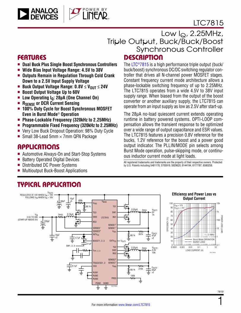
TYPICAL APPLICATION
Low IQ, 2.25MHz, Triple Output, Buck/Buck/Boost
Synchronous Controller
The LTC®7815 is a high performance triple output (buck/buck/boost) synchronous DC/DC switching regulator con-troller that drives all N-channel power MOSFET stages. Constant frequency current mode architecture allows a phase-lockable switching frequency of up to 2.25MHz. The LTC7815 operates from a wide 4.5V to 38V input supply range. When biased from the output of the boost converter or another auxiliary supply, the LTC7815 can operate from an input supply as low as 2.5V after start-up.
The 28μA no-load quiescent current extends operating runtime in battery powered systems. OPTI-LOOP com-pensation allows the transient response to be optimized over a wide range of output capacitance and ESR values. The LTC7815 features a precision 0.8V reference for the bucks, 1.2V reference for the boost and a power good output indicator. The PLLIN/MODE pin selects among Burst Mode operation, pulse-skipping mode, or continu-ous inductor current mode at light loads.All registered trademarks and trademarks are the property of their respective owners. Protected by U.S. Patents including 5481178, 5705919, 5929620, 6144194, 6177787, 6580258.
FEATURES
APPLICATIONS
n Dual Buck Plus Single Boost Synchronous Controllersn Wide Bias Input Voltage Range: 4.5V to 38Vn Outputs Remain in Regulation Through Cold Crank
Down to a 2.5V Input Supply Voltagen Buck Output Voltage Range: 0.8V ≤ VOUT ≤ 24Vn Boost Output Voltage Up to 60Vn Low Operating IQ: 28μA (One Channel On)n RSENSE or DCR Current Sensingn 100% Duty Cycle for Boost Synchronous MOSFET
Even in Burst Mode® Operationn Phase-Lockable Frequency (320kHz to 2.25MHz)n Programmable Fixed Frequency (320kHz to 2.25MHz)n Very Low Buck Dropout Operation: 98% Duty Cyclen Small 38-Lead 5mm × 7mm QFN Package
n Automotive Always-On and Start-Stop Systemsn Battery Operated Digital Devicesn Distributed DC Power Systemsn Multioutput Buck-Boost Applications
Efficiency and Power Loss vs Output Current
VIN = 12VVOUT1 = 5V
Burst Mode OPERATIONBURST LOSS
LOAD CURRENT (A)0.0001 0.001 0.01 0.1 1 100
10
20
30
40
50
60
70
80
90
100
0.1
1
10
100
1k
10k
EFFI
CIEN
CY (%
)
POWER LOSS (m
W)
7815 TA01b
f = 2.1MHz
7815 TA01a
LTC7815
VFB3
TG3
BG3
SENSE3–
SENSE3+
INTVCC
BOOST1, 2, 3
ITH1, 2, 3
TRACK/SS1, 2
SW1
SENSE1+
SENSE1–
VFB1
EXTVCC
TG2SW2BG2
SENSE2+
SENSE2–
VFB2
PGND
RUN1RUN2RUN3
SS3
SGND
FREQ
0.33µH 3mΩ
357k COUT147µF×2
68.1k
68.1k
210k
100k
COUT233µF×2
68.1k
0.16µH3mΩ
499k VBIAS
4.7µF
SW1, 2, 30.1µF
0.1µF
VIN2.5V TO 28V
(START-UP ABOVE 5V)
VOUT15V7A
VOUT1
VOUT23.3V10A
68µF10µF×5
220µF
10µF×2
VOUT3REGULATED AT 10V WHEN VIN < 10V
FOLLOWS VIN WHEN VIN > 10V
0.33µH 3mΩ
TG1
SW3 BG1
+
+

LTC7815
27815f
For more information www.linear.com/LTC7815
ABSOLUTE MAXIMUM RATINGSBias Input Supply Voltage (VBIAS) .............. –0.3V to 40VBuck Top Side Driver Voltages (BOOST1, BOOST2) ............................. –0.3V to 46VBoost Top Side Driver Voltages (BOOST3) ............................................ –0.3V to 71VBuck Switch Voltage (SW1, SW2) ................ –5V to 40VBoost Switch Voltage (SW3) ........................ –5V to 65VINTVCC, (BOOST1–SW1), (BOOST2–SW2), (BOOST3–SW3) ........... –0.3V to 6V BG1, BG2, BG3, TG1, TG2, TG3 ...................... (Note 8)RUN1, RUN2, RUN3 .................................... –0.3V to 8V
Maximum Current Sourced Into Pin from Source >8V ..............................................100µA
(Note 1)
13 14 15 16
TOP VIEW
39PGND
UHF PACKAGE38-LEAD (5mm × 7mm) PLASTIC QFN
17 18 19
38 37 36 35 34 33 32
24
25
26
27
28
29
30
31
8
7
6
5
4
3
2
1FREQ
PLLIN/MODE
SS3
SENSE3+
SENSE3–
VFB3
ITH3
SGND
RUN1
RUN2
RUN3
SENSE2–
SW1
BOOST1
BG1
SW3
TG3
BOOST3
BG3
VBIAS
EXTVCC
INTVCC
BG2
BOOST2
SENS
E1–
SENS
E1+
V FB1
I TH1
TRAC
K/SS
1
PGOO
D1
TG1
SENS
E2+
V FB2
I TH2
TRAC
K/SS
2
OV3
TG2
SW2
23
22
21
20
9
10
11
12
TJMAX = 150°C, qJA = 34.7°C/W, qJC = 2°C/W
EXPOSED PAD (PIN 39) IS PGND, MUST BE SOLDERED TO PCB
PIN CONFIGURATION
SENSE1+, SENSE2+, SENSE1–
SENSE2– Voltages ................................. –0.3V to 28VSENSE3+, SENSE3– Voltages ..................... –0.3V to 40VFREQ Voltages ......................................–0.3V to INTVCCEXTVCC ...................................................... –0.3V to 14VITH1, ITH2, ITH3, VFB1, VFB2, VFB3 Voltages .... –0.3V to 6VPLLIN/MODE, PGOOD1, OV3 Voltages ........ –0.3V to 6VTRACK/SS1, TRACK/SS2, SS3 Voltages ..... –0.3V to 6VOperating Junction Temperature Range (Notes 2, 3)
LTC7815E, LTC7815I .......................... –40°C to 125°C LTC7815H .......................................... –40°C to 150°C Storage Temperature Range .............. –65°C to 150°C
LTC7815
37815f
For more information www.linear.com/LTC7815
ELECTRICAL CHARACTERISTICS
ORDER INFORMATION
SYMBOL PARAMETER CONDITIONS MIN TYP MAX UNITS
VBIAS Bias Input Supply Operating Voltage Range
4.5 38 V
VFB1,2 Buck Regulated Feedback Voltage (Note 4); ITH1,2 Voltage = 1.2V 0°C to 85°C, All Grades LTC7815E, LTC7815I LTC7815H
l
l
0.792 0.788 0.786
0.800 0.800 0.800
0.808 0.812 0.812
V V V
VFB3 Boost Regulated Feedback Voltage (Note 4); ITH3 Voltage = 1.2V 0°C to 85°C, All Grades LTC7815E, LTC7815I LTC7815H
l
l
1.183 1.181 1.176
1.200 1.200 1.200
1.214 1.218 1.218
V V V
IFB1,2,3 Feedback Current (Note 4) –2 ±50 nA
VREFLNREG Reference Voltage Line Regulation (Note 4); VIN = 4.5V to 38V 0.002 0.02 %/V
VLOADREG Output Voltage Load Regulation (Note 4)
Measured in Servo Loop; ∆ITH Voltage = 1.2V to 0.7V
l 0.01 0.1 %
Measured in Servo Loop; ∆ITH Voltage = 1.2V to 2V
l –0.01 –0.1 %
gm1,2,3 Transconductance Amplifier gm (Note 4); ITH1,2,3 = 1.2V; Sink/Source 5µA
2 mmho
The l denotes the specifications which apply over the specified operating junction temperature range, otherwise specifications are at TA = 25°C (Notes 2, 4). VBIAS = 12V, VRUN1,2,3 = 5V, EXTVCC = 0V unless otherwise noted.
LEAD FREE FINISH TAPE AND REEL PART MARKING* PACKAGE DESCRIPTION TEMPERATURE RANGE
LTC7815EUHF#PBF LTC7815EUHF#TRPBF 7815 38-Lead (5mm × 7mm) Plastic QFN –40°C to 125°C
LTC7815IUHF#PBF LTC7815IUHF#TRPBF 7815 38-Lead (5mm × 7mm) Plastic QFN –40°C to 125°C
LTC7815HUHF#PBF LTC7815HUHF#TRPBF 7815 38-Lead (5mm × 7mm) Plastic QFN –40°C to 150°C
Consult ADI Marketing for parts specified with wider operating temperature ranges. *The temperature grade is identified by a label on the shipping container.For more information on lead free part marking, go to: http://www.linear.com/leadfree/ For more information on tape and reel specifications, go to: http://www.linear.com/tapeandreel/. Some packages are available in 500 unit reels through designated sales channels with #TRMPBF suffix.
http://www.linear.com/product/LTC7815#orderinfo
LTC7815
47815f
For more information www.linear.com/LTC7815
ELECTRICAL CHARACTERISTICS The l denotes the specifications which apply over the specified operating junction temperature range, otherwise specifications are at TA = 25°C (Notes 2, 4). VBIAS = 12V, VRUN1,2,3 = 5V, EXTVCC = 0V unless otherwise noted.
SYMBOL PARAMETER CONDITIONS MIN TYP MAX UNITS
IQ Input DC Supply Current (Note 5)
Pulse-Skipping or Forced Continuous Mode (One Channel On)
RUN1 = 5V and RUN2,3 = 0V or RUN2 = 5V and RUN1,3 = 0V or RUN3 = 5V and RUN1,2 = 0V VFB1, 2 ON = 0.83V (No Load) VFB3 = 1.25V
1.5 mA
Pulse-Skipping or Forced Continuous Mode (All Channels On)
RUN1,2,3 = 5V, VFB1,2 = 0.83V (No Load) VFB3 = 1.25V
3 mA
Sleep Mode (One Channel On, Buck)
RUN1 = 5V and RUN2,3 = 0V or RUN2 = 5V and RUN1,3 = 0V VFB,ON = 0.83V (No Load)
l
l
28 35
48 59
µA
Sleep Mode (One Channel On, Boost)
RUN3 = 5V and RUN1,2 = 0V VFB3 = 1.25V
33 53 µA
Sleep Mode (Buck and Boost Channel On)
RUN1 = 5V and RUN2 = 0V or RUN2 = 5V and RUN1 = 0V RUN3 = 5V VFB1,2 = 0.83V (No Load) VFB3 = 1.25V
33 40
46 59
µA
Sleep Mode (All Three Channels On)
RUN1,2,3 = 5V, VFB1,2 = 0.83V (No Load) VFB3 = 1.25V
38 56 µA
Shutdown RUN1,2,3 = 0V 10 20 µA
UVLO Undervoltage Lockout INTVCC Ramping Up l 4.15 4.5 V
INTVCC Ramping Down l 3.5 3.8 4.0 V
VOVL1,2 Buck Feedback Overvoltage Protection Measured at VFB1,2 Relative to Regulated VFB1,2
7 10 13 %
ISENSE1,2+ SENSE+ Pin Current Bucks (Channels 1 and 2) VOUT = 3.3V ±1 µA
ISENSE3+ SENSE+ Pin Current Boost (Channel 3) 170 µA
ISENSE1,2– SENSE– Pin Current Bucks (Channels 1 and 2) VOUT = 3.3V VOUT1,2 > VINTVCC + 0.5V
700
±2
µA µA
ISENSE3– SENSE– Pin Current Boost (Channel 3) VSENSE3+, VSENSE3– = 12V
±1 µA
DFMAX,TG Maximum Duty Factor for TG Bucks (Channels 1,2) in Dropout, FREQ = 0V Boost (Channel 3) in Overvoltage
97 98 100
% %
DFMAX,BG Maximum Duty Factor for BG Bucks (Channels 1,2) in Overvoltage Boost (Channel 3)
100 90
% %
ITRACK/SS1,2 Soft-Start Charge Current VTRACK/SS1,2 = 0V 3 5 8 µA
ISS3 Soft-Start Charge Current VSS3 = 0V 3 5 8 µA
VRUN1 ON VRUN2,3 ON
RUN1 Pin Threshold RUN2,3 Pin Threshold
VRUN1 Rising VRUN2,3 Rising
l
l
1.18 1.21
1.24 1.27
1.32 1.33
V V
VRUN1,2,3 Hyst RUN Pin Hysteresis 70 mV
VSENSE1,2,3(MAX) Maximum Current Sense Threshold VFB1,2 = 0.7V, VSENSE1,2– = 3.3V VFB1,2,3 = 1.1V, VSENSE3+ = 12V
l 43 50 57 mV
VSENSE3(CM) SENSE3 Pins Common Mode Range (BOOST Converter Input Supply Voltage)
2.5 38 V
LTC7815
57815f
For more information www.linear.com/LTC7815
ELECTRICAL CHARACTERISTICS The l denotes the specifications which apply over the specified operating junction temperature range, otherwise specifications are at TA = 25°C (Notes 2, 4). VBIAS = 12V, VRUN1,2,3 = 5V, EXTVCC = 0V unless otherwise noted.
SYMBOL PARAMETER CONDITIONS MIN TYP MAX UNITS
Gate Driver
TG1,2 Pull-Up On-Resistance Pull-Down On-Resistance
2.5 1.5
Ω Ω
BG1,2 Pull-Up On-Resistance Pull-Down On-Resistance
2.4 1.1
Ω Ω
TG3 Pull-Up On-Resistance Pull-Down On-Resistance
1.2 1.0
Ω Ω
BG3 Pull-Up On-Resistance Pull-Down On-Resistance
1.2 1.0
Ω Ω
TG1,2,3 tr TG1,2,3 tf
TG Transition Time: Rise Time Fall Time
(Note 6) CLOAD = 3300pF CLOAD = 3300pF
25 16
ns ns
BG1,2,3 tr BG1,2,3 tf
BG Transition Time: Rise Time Fall Time
(Note 6) CLOAD = 3300pF CLOAD = 3300pF
28 13
ns ns
TG/BG t1D Top Gate Off to Bottom Gate On Delay Synchronous Switch-On Delay Time
CLOAD = 3300pF Each Driver Bucks (Channels 1, 2) Boost (Channel 3)
25 30
ns ns
BG/TG t1D Bottom Gate Off to Top Gate On Delay Top Switch-On Delay Time
CLOAD = 3300pF Each Driver Bucks (Channels 1, 2) Boost (Channel 3)
20 20
ns ns
tON(MIN)1,2 Buck Minimum On-Time (Note 7) 45 ns
tON(MIN)3 Boost Minimum On-Time (Note 7) 70 ns
INTVCC Linear Regulator
VINTVCCVBIAS Internal VCC Voltage 6V < VBIAS < 38V, VEXTVCC = 0V, IINTVCC = 0mA 5.0 5.4 5.6 V
VLDOVBIAS INTVCC Load Regulation ICC = 0mA to 100mA, VEXTVCC = 0V 0.8 2.5 %
VINTVCCEXT Internal VCC Voltage 6V < VEXTVCC < 13V, IINTVCC = 0mA 5.0 5.4 5.6 V
VLDOEXT INTVCC Load Regulation ICC = 0mA to 100mA, VEXTVCC = 8.5V 0.8 2.5 %
VEXTVCC EXTVCC Switchover Voltage EXTVCC Ramping Positive 4.5 4.7 V
VLDOHYS EXTVCC Hysteresis 200 mV
Oscillator and Phase-Locked Loop
f25k Programmable Frequency RFREQ = 25k; PLLIN/MODE = DC Voltage 0.25 0.32 0.37 MHz
f65k Programmable Frequency RFREQ = 65k; PLLIN/MODE = DC Voltage 1.18 MHz
f100k Programmable Frequency RFREQ = 100k; PLLIN/MODE = DC Voltage l 1.75 2.1 2.4 MHz
fLOW Low Fixed Frequency VFREQ = 0V PLLIN/MODE = DC Voltage 0.77 0.94 1.13 MHz
fHIGH High Fixed Frequency VFREQ = INTVCC; PLLIN/MODE = DC Voltage 1.2 1.44 1.75 MHz
fSYNC Synchronizable Frequency PLLIN/MODE = External Clock l 0.32 2.25 MHz
PLLIN VIH PLLIN/MODE Input High Level PLLIN/MODE = External Clock l 2.5 V
PLLIN VIL PLLIN/MODE Input Low Level PLLIN/MODE = External Clock l 0.5 V
LTC7815
67815f
For more information www.linear.com/LTC7815
Note 1: Stresses beyond those listed under Absolute Maximum Ratings may cause permanent damage to the device. Exposure to any Absolute Maximum Rating condition for extended periods may affect device reliability and lifetime.Note 2: The LTC7815 is tested under pulsed load conditions such that TJ ≈ TA. The LTC7815E is guaranteed to meet performance specifications from 0°C to 85°C. Specifications over the –40°C to 125°C operating junction temperature range are assured by design, characterization and correlation with statistical process controls. The LTC7815I is guaranteed over the –40°C to 125°C operating junction temperature range and the LTC7815H is guaranteed over the –40°C to 150°C operating junction temperature range. High junction temperatures degrade operating lifetimes; operating lifetime is derated for junction temperatures greater than 125°C. Note that the maximum ambient temperature consistent with these specifications is determined by specific operating conditions in conjunction with board layout, the rated package thermal impedance and other environmental factors. TJ is calculated from the ambient temperature TA and power dissipation PD according to the following formula: TJ = TA + (PD • θJA), where θJA = 34.7°C/W.Note 3: This IC includes overtemperature protection that is intended to protect the device during momentary overload conditions. The maximum rated junction temperature will be exceeded when this protection is active.
Continuous operation above the specified absolute maximum operating junction temperature may impair device reliability or permanently damage the device.Note 4: The LTC7815 is tested in a feedback loop that servos VITH1,2,3 to a specified voltage and measures the resultant VFB. The specification at 85°C is not tested in production and is assured by design, characterization and correlation to production testing at other temperatures (125°C for the LTC7815E/LTC7815I, 150°C for the LTC7815H). For the LTC7815I and LTC7815H, the specification at 0°C is not tested in production and is assured by design, characterization and correlation to production testing at –40°C.Note 5: Dynamic supply current is higher due to the gate charge being delivered at the switching frequency. See the Applications Information section.Note 6: Rise and fall times are measured using 10% and 90% levels. Delay times are measured using 50% levels.Note 7: The minimum on-time condition is specified for an inductor peak-to-peak ripple current ≥ 40% of IMAX (See the Minimum On-Time Considerations in the Applications Information section).Note 8: Do not apply a voltage or current source to these pins. They must be connected to capacitive loads only, otherwise permanent damage may occur.
ELECTRICAL CHARACTERISTICS
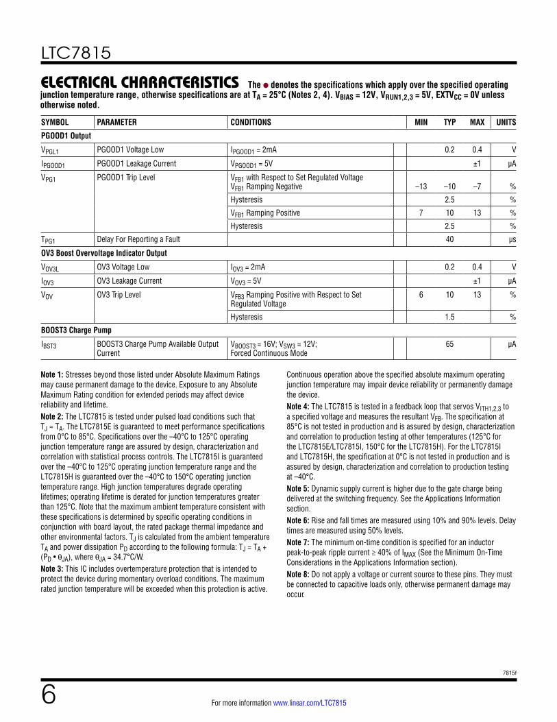
SYMBOL PARAMETER CONDITIONS MIN TYP MAX UNITS
PGOOD1 Output
VPGL1 PGOOD1 Voltage Low IPGOOD1 = 2mA 0.2 0.4 V
IPGOOD1 PGOOD1 Leakage Current VPGOOD1 = 5V ±1 µA
VPG1 PGOOD1 Trip Level VFB1 with Respect to Set Regulated Voltage VFB1 Ramping Negative
–13
–10
–7
%
Hysteresis 2.5 %
VFB1 Ramping Positive 7 10 13 %
Hysteresis 2.5 %
TPG1 Delay For Reporting a Fault 40 µs
OV3 Boost Overvoltage Indicator Output
VOV3L OV3 Voltage Low IOV3 = 2mA 0.2 0.4 V
IOV3 OV3 Leakage Current VOV3 = 5V ±1 µA
VOV OV3 Trip Level VFB3 Ramping Positive with Respect to Set Regulated Voltage
6 10 13 %
Hysteresis 1.5 %
BOOST3 Charge Pump
IBST3 BOOST3 Charge Pump Available Output Current
VBOOST3 = 16V; VSW3 = 12V; Forced Continuous Mode
65 µA
The l denotes the specifications which apply over the specified operating junction temperature range, otherwise specifications are at TA = 25°C (Notes 2, 4). VBIAS = 12V, VRUN1,2,3 = 5V, EXTVCC = 0V unless otherwise noted.
LTC7815
77815f
For more information www.linear.com/LTC7815
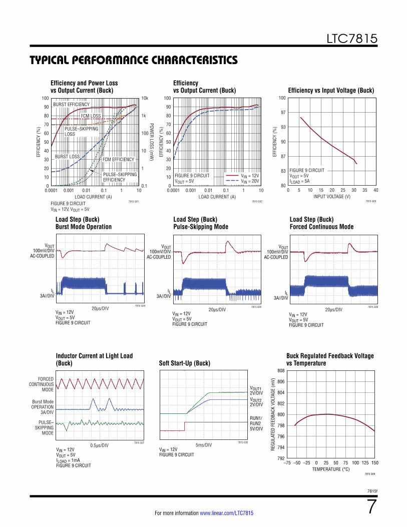
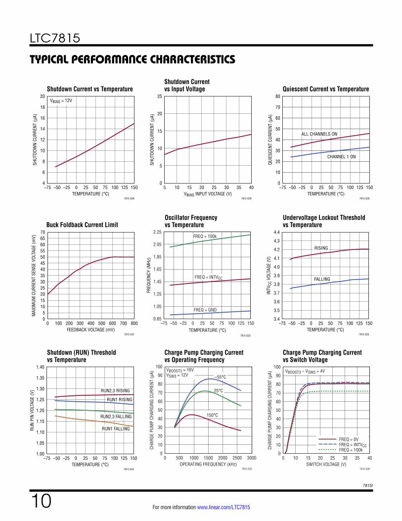
TYPICAL PERFORMANCE CHARACTERISTICS
Load Step (Buck) Burst Mode Operation
Load Step (Buck) Forced Continuous Mode
Load Step (Buck) Pulse-Skipping Mode
Inductor Current at Light Load (Buck) Soft Start-Up (Buck)
Buck Regulated Feedback Voltage vs Temperature
Efficiency and Power Loss vs Output Current (Buck)
Efficiency vs Output Current (Buck) Efficiency vs Input Voltage (Buck)
TEMPERATURE (°C)–75
REGU
LATE
D FE
EDBA
CK V
OLTA
GE (m
V)
808
806
802
798
794
804
800
796
7920 25 50 75 150125100–50
7815 G09
–25
FIGURE 9 CIRCUITVOUT = 5VILOAD = 5A
INPUT VOLTAGE (V)0 5 10 15 20 25 30 35 40
80
83
87
90
93
97
100
EFFI
CIEN
CY (%
)
7815 G03
5ms/DIV7815 G08
VOUT12V/DIVVOUT22V/DIV
RUN1/RUN25V/DIV
VIN = 12VFIGURE 9 CIRCUIT
BURST EFFICIENCY
FCM LOSS
PULSE–SKIPPINGLOSS
BURST LOSS FCM EFFICIENCY
PULSE–SKIPPINGEFFICIENCY
LOAD CURRENT (A)0.0001 0.001 0.01 0.1 1 10
FIGURE 9 CIRCUITVIN = 12V, VOUT = 5V
0
10
20
30
40
50
60
70
80
90
100
0.1
1
10
100
1k
10k
EFFI
CIEN
CY (%
)
POWER LOSS (m
W)
7815 G01
FIGURE 9 CIRCUITVOUT = 5V
VIN = 12VVIN = 20V
LOAD CURRENT (A)0.0001 0.001 0.01 0.1 1 100
10
20
30
40
50
60
70
80
90
100
EFFI
CIEN
CY (%
)
7815 G02
0.5µs/DIV
FORCEDCONTINUOUS
MODE
Burst ModeOPERATION
3A/DIV
PULSE–SKIPPING
MODE
7815 G07
VIN = 12VVOUT = 5VILOAD = 1mAFIGURE 9 CIRCUIT
20µs/DIV7815 G04
VOUT100mV/DIV
AC-COUPLED
IL3A//DIV
VIN = 12VVOUT = 5VFIGURE 9 CIRCUIT
VOUT100mV/DIV
AC-COUPLED
IL3A//DIV
VIN = 12VVOUT = 5VFIGURE 9 CIRCUIT
20µs/DIV7815 G05
VOUT100mV/DIV
AC-COUPLED
IL3A//DIV
VIN = 12VVOUT = 5VFIGURE 9 CIRCUIT
20µs/DIV7815 G06
LTC7815
87815f
For more information www.linear.com/LTC7815
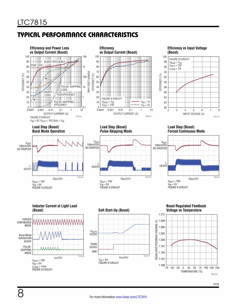
TYPICAL PERFORMANCE CHARACTERISTICS
Load Step (Boost) Burst Mode Operation
Load Step (Boost) Pulse-Skipping Mode
Load Step (Boost) Forced Continuous Mode
Inductor Current at Light Load (Boost) Soft Start-Up (Boost)
Boost Regulated Feedback Voltage vs Temperature
Efficiency and Power Loss vs Output Current (Boost)
Efficiency vs Output Current (Boost)
Efficiency vs Input Voltage (Boost)
TEMPERATURE (°C)–75
REGU
LATE
D FE
EDBA
CK V
OLTA
GE (V
)
1.212
1.209
1.203
1.191
1.194
1.197
1.206
1.200
1.1880 25 50 75 150120100–50
7815 G18
–25
FIGURE 9 CIRCUITVBIAS = VINVOUT = 10VILOAD = 2A
INPUT VOLTAGE (V)2 3 4 5 6 7 8
80
82
84
86
88
90
92
94
96
98
100
EFFI
CIEN
CY (%
)
7815 G12
5ms/DIV7815 G17
RUN35V/DIV
VOUT32V/DIV
GND
VIN = 5VFIGURE 9 CIRCUIT
BURST EFFICIENCYFCM LOSS
PULSE–SKIPPINGLOSS
FCM EFFICIENCYBURSTLOSS
PULSE–SKIPPINGEFFICIENCY
OUTPUT CURRENT (A)0.0001 0.001 0.01 0.1 1 100
10
20
30
40
50
60
70
80
90
100
0.1
1
10
100
1k
10k
EFFI
CIEN
CY (%
)
POWER LOSS (m
W)
7815 G10FIGURE 9 CIRCUITVIN = 5V, VOUT = 10V, Bias = VIN
FIGURE 9 CIRCUITVBIAS = VINVOUT = 10V
VIN = 7VVIN = 5V
OUTPUT CURRENT (A)0.0001 0.001 0.01 0.1 1 100
10
20
30
40
50
60
70
80
90
100
EFFI
CIEN
CY (%
)
7815 G11
50µs/DIV
IL5A/DIV
7815 G13
VOUT100mV/DIV
AC-COUPLED
VOUT = 10VVIN = 5VFIGURE 9 CIRCUIT
50µs/DIV7815 G14
VOUT100mV/DIV
AC-COUPLED
IL5A/DIV
VOUT = 10VVIN = 5VFIGURE 9 CIRCUIT
50µs/DIV7815 G15
VOUT100mV/DIV
AC-COUPLED
IL5A/DIV
VOUT = 10VVIN = 5VFIGURE 9 CIRCUIT
FORCEDCONTINUOUS
MODE
Burst ModeOPERATION
5A/DIV
PULSE-SKIPPING
MODE
VOUT = 10VVIN = 5VILOAD = 1mAFIGURE 9 CIRCUIT
1µs/DIV7815 G16
LTC7815
97815f
For more information www.linear.com/LTC7815
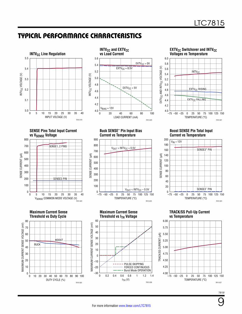
TYPICAL PERFORMANCE CHARACTERISTICS
SENSE Pins Total Input Current vs VSENSE Voltage
Buck SENSE– Pin Input Bias Current vs Temperature
Boost SENSE Pin Total Input Current vs Temperature
INTVCC Line RegulationINTVCC and EXTVCC vs Load Current
EXTVCC Switchover and INTVCC Voltages vs Temperature
INPUT VOLTAGE (V)0
INTV
CC V
OLTA
GE (V
)
5.5
5.4
5.2
5.3
5.1
5.015 20 25 30 35 405
7815 G19
10LOAD CURRENT (mA)
0
INTV
CC V
OLTA
GE (V
)
5.6
5.2
5.4
4.6
4.8
5.0
4.4
4.2
4.060 80 10020
7815 G20
40
EXTVCC = 0V
EXTVCC = 5V
EXTVCC = 8.5V
VBIAS = 12V
TEMPERATURE (°C)–75
EXTV
CC A
ND IN
TVCC
VOL
TAGE
(V)
6.0
5.8
5.4
5.2
4.4
4.2
4.6
4.8
5.6
5.0
4.00 25 50 75 150125100–50
7815 G21
–25
INTVCC
EXTVCC RISING
EXTVCC FALLING
VSENSE COMMON MODE VOLTAGE (V)0
SENS
E CU
RREN
T (µ
A)
800
700
400
500
300
100
200
600
015 20 25 30 35 405
7815 G22
10
SENSE1, 2 PINS
SENSE3 PIN
TEMPERATURE (°C)–75
SENS
E CU
RREN
T (µ
A)
900
700
800
400
500
300
100
200
600
00 25 50 75 100 125 150–50
7815 G23
–25
VOUT < INTVCC – 0.5V
VOUT > INTVCC + 0.5V
TEMPERATURE (°C)–75
SENS
E CU
RREN
T (µ
A)
200
160
180
100
120
80
40
20
60
140
00 25 50 75 100 125 150–50
7815 G24
–25
SENSE3+ PIN
SENSE3– PIN
VIN = 12V
Maximum Current Sense Threshold vs Duty Cycle
Maximum Current Sense Threshold vs ITH Voltage
TRACK/SS Pull-Up Current vs Temperature
DUTY CYCLE (%)0
MAX
IMUM
CUR
RENT
SEN
SE V
OLTA
GE (m
V)
80
60
70
30
40
20
10
50
050 60 70 80 90 10010
7815 G25
20 30 40
BOOST
BUCK
ITH (V)0
MAX
IMUM
CUR
RENT
SEN
SE V
OLTA
GE (m
V)
60
40
50
–10
0
–20
30
20
10
–301 1.2 1.40.2
7815 G26
0.4 0.6 0.8
Burst Mode OPERATION
PULSE-SKIPPINGFORCED CONTINUOUS
TEMPERATURE (°C)–75
TRAC
K/SS
CUR
RENT
(µA)
6.00
5.75
5.25
5.00
4.25
4.50
5.50
4.75
4.000 25 50 75 125100 150–50
7815 G27
–25
LTC7815
107815f
For more information www.linear.com/LTC7815
TYPICAL PERFORMANCE CHARACTERISTICS
Buck Foldback Current LimitOscillator Frequency vs Temperature
Undervoltage Lockout Threshold vs Temperature
Shutdown (RUN) Threshold vs Temperature
Charge Pump Charging Current vs Operating Frequency
Charge Pump Charging Current vs Switch Voltage
Shutdown Current vs TemperatureShutdown Current vs Input Voltage Quiescent Current vs Temperature
TEMPERATURE (°C)–75
SHUT
DOW
N CU
RREN
T (µ
A)
20
16
14
10
18
12
4
6
8
0 25 50 75 100 125 150–50
7815 G28
–25
VBIAS = 12V
VBIAS INPUT VOLTAGE (V)5
SHUT
DOW
N CU
RREN
T (µ
A)
25
20
15
5
10
020 25 30 35 4010
7815 G29
15TEMPERATURE (°C)
–75
QUIE
SCEN
T CU
RREN
T (µ
A)
80
50
60
70
0
10
20
30
40
0 25 50 75 100 125 150–50
7815 G30
–25
CHANNEL 1 ON
ALL CHANNELS ON
FEEDBACK VOLTAGE (mV)0
MAX
IMUM
CUR
RENT
SEN
SE V
OLTA
GE (m
V)
70
60
50
20
10
30
40
65
55
45
15
5
25
35
0300 400 500 600 700 800100
7815 G31
200TEMPERATURE (°C)
–75
INTV
CC V
OLTA
GE (V
)
4.4
4.3
4.2
3.6
3.8
4.0
3.4
3.5
3.7
3.9
4.1
0 25 50 75 100 125 150–50
7815 G33
–25
RISING
FALLING
TEMPERATURE (°C)–75
RUN
PIN
VOLT
AGE
(V)
1.40
1.35
1.30
1.20
1.00
1.15
1.10
1.05
1.25
0 25 50 75 100 125 150–50
7815 G34
–25
RUN1 RISING
RUN1 FALLING
RUN2,3 FALLING
RUN2,3 RISING
VBOOST3 – VSW3 = 4V
FREQ = 0VFREQ = INTVCCFREQ = 100k
SWITCH VOLTAGE (V)5 10 15 20 25 30 35 40
0
10
20
30
40
50
60
70
80
90
100
CHAR
GE P
UMP
CHAR
GING
CUR
RENT
(µA)
7815 G36
TEMPERATURE (°C)
FREQ
UENC
Y (M
Hz)
7815 G32
FREQ = 100k
FREQ = INTVCC
FREQ = GND
–75 –50 –25 0 25 50 75 100 125 1500.85
1.05
1.25
1.45
1.65
1.85
2.05
2.25
VBOOST3 = 16VVSW3 = 12V –55°C
25°C
150°C
OPERATING FREQUENCY (kHz)0 500 1000 1500 2000 2500 3000
0
10
20
30
40
50
60
70
80
90
100
CHAR
GE P
UMP
CHAR
GING
CUR
RENT
(µA)
7815 G35
LTC7815
117815f
For more information www.linear.com/LTC7815
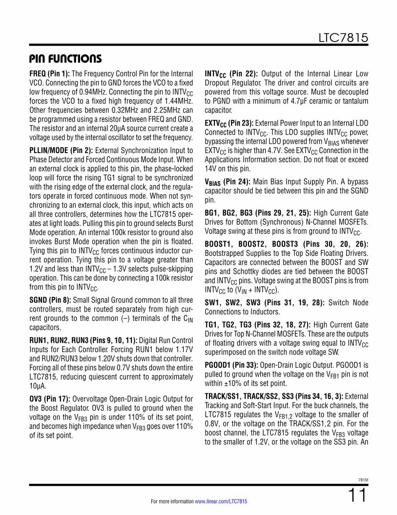
PIN FUNCTIONSFREQ (Pin 1): The Frequency Control Pin for the Internal VCO. Connecting the pin to GND forces the VCO to a fixed low frequency of 0.94MHz. Connecting the pin to INTVCC forces the VCO to a fixed high frequency of 1.44MHz. Other frequencies between 0.32MHz and 2.25MHz can be programmed using a resistor between FREQ and GND. The resistor and an internal 20µA source current create a voltage used by the internal oscillator to set the frequency.
PLLIN/MODE (Pin 2): External Synchronization Input to Phase Detector and Forced Continuous Mode Input. When an external clock is applied to this pin, the phase-locked loop will force the rising TG1 signal to be synchronized with the rising edge of the external clock, and the regula-tors operate in forced continuous mode. When not syn-chronizing to an external clock, this input, which acts on all three controllers, determines how the LTC7815 oper-ates at light loads. Pulling this pin to ground selects Burst Mode operation. An internal 100k resistor to ground also invokes Burst Mode operation when the pin is floated. Tying this pin to INTVCC forces continuous inductor cur-rent operation. Tying this pin to a voltage greater than 1.2V and less than INTVCC – 1.3V selects pulse-skipping operation. This can be done by connecting a 100k resistor from this pin to INTVCC.
SGND (Pin 8): Small Signal Ground common to all three controllers, must be routed separately from high cur-rent grounds to the common (–) terminals of the CIN capacitors.
RUN1, RUN2, RUN3 (Pins 9, 10, 11): Digital Run Control Inputs for Each Controller. Forcing RUN1 below 1.17V and RUN2/RUN3 below 1.20V shuts down that controller. Forcing all of these pins below 0.7V shuts down the entire LTC7815, reducing quiescent current to approximately 10µA.
OV3 (Pin 17): Overvoltage Open-Drain Logic Output for the Boost Regulator. OV3 is pulled to ground when the voltage on the VFB3 pin is under 110% of its set point, and becomes high impedance when VFB3 goes over 110% of its set point.
INTVCC (Pin 22): Output of the Internal Linear Low Dropout Regulator. The driver and control circuits are powered from this voltage source. Must be decoupled to PGND with a minimum of 4.7µF ceramic or tantalum capacitor.
EXTVCC (Pin 23): External Power Input to an Internal LDO Connected to INTVCC. This LDO supplies INTVCC power, bypassing the internal LDO powered from VBIAS whenever EXTVCC is higher than 4.7V. See EXTVCC Connection in the Applications Information section. Do not float or exceed 14V on this pin.
VBIAS (Pin 24): Main Bias Input Supply Pin. A bypass capacitor should be tied between this pin and the SGND pin.
BG1, BG2, BG3 (Pins 29, 21, 25): High Current Gate Drives for Bottom (Synchronous) N-Channel MOSFETs. Voltage swing at these pins is from ground to INTVCC.
BOOST1, BOOST2, BOOST3 (Pins 30, 20, 26): Bootstrapped Supplies to the Top Side Floating Drivers. Capacitors are connected between the BOOST and SW pins and Schottky diodes are tied between the BOOST and INTVCC pins. Voltage swing at the BOOST pins is from INTVCC to (VIN + INTVCC).
SW1, SW2, SW3 (Pins 31, 19, 28): Switch Node Connections to Inductors.
TG1, TG2, TG3 (Pins 32, 18, 27): High Current Gate Drives for Top N-Channel MOSFETs. These are the outputs of floating drivers with a voltage swing equal to INTVCC superimposed on the switch node voltage SW.
PGOOD1 (Pin 33): Open-Drain Logic Output. PGOOD1 is pulled to ground when the voltage on the VFB1 pin is not within ±10% of its set point.
TRACK/SS1, TRACK/SS2, SS3 (Pins 34, 16, 3): External Tracking and Soft-Start Input. For the buck channels, the LTC7815 regulates the VFB1,2 voltage to the smaller of 0.8V, or the voltage on the TRACK/SS1,2 pin. For the boost channel, the LTC7815 regulates the VFB3 voltage to the smaller of 1.2V, or the voltage on the SS3 pin. An
LTC7815
127815f
For more information www.linear.com/LTC7815
PIN FUNCTIONSinternal 5µA pull-up current source is connected to this pin. A capacitor to ground at this pin sets the ramp time to final regulated output voltage. Alternatively, a resis-tor divider on another voltage supply connected to the TRACK/SS pins of the buck channels allow the LTC7815 buck outputs to track the other supply during start-up.
ITH1, ITH2, ITH3 (Pins 35, 15, 7): Error Amplifier Outputs and Switching Regulator Compensation Points. Each associated channel’s current comparator trip point increases with this control voltage.
VFB1, VFB2, VFB3 (Pins 36, 14, 6): Receives the remotely sensed feedback voltage for each controller from an exter-nal resistive divider across the output.
SENSE1+, SENSE2+, SENSE3+ (Pins 37, 13, 4): The (+) Input to the Differential Current Comparators. The ITH pin voltage and controlled offsets between the SENSE– and SENSE+ pins in conjunction with RSENSE set the current trip threshold. For the boost channel, the SENSE3+ pin supplies current to the current comparator.
SENSE1–, SENSE2–, SENSE3– (Pins 38, 12, 5): The (–) Input to the Differential Current Comparators. When SENSE1,2– for the buck channels is greater than INTVCC, then SENSE1,2– pin supplies current to the current comparator.
PGND (Exposed Pad Pin 39): Driver Power Ground. Connects to the sources of bottom N-channel MOSFETs and the (–) terminal(s) of CIN. The exposed pad must be soldered to the PCB for rated electrical and thermal performance.
LTC7815
137815f
For more information www.linear.com/LTC7815
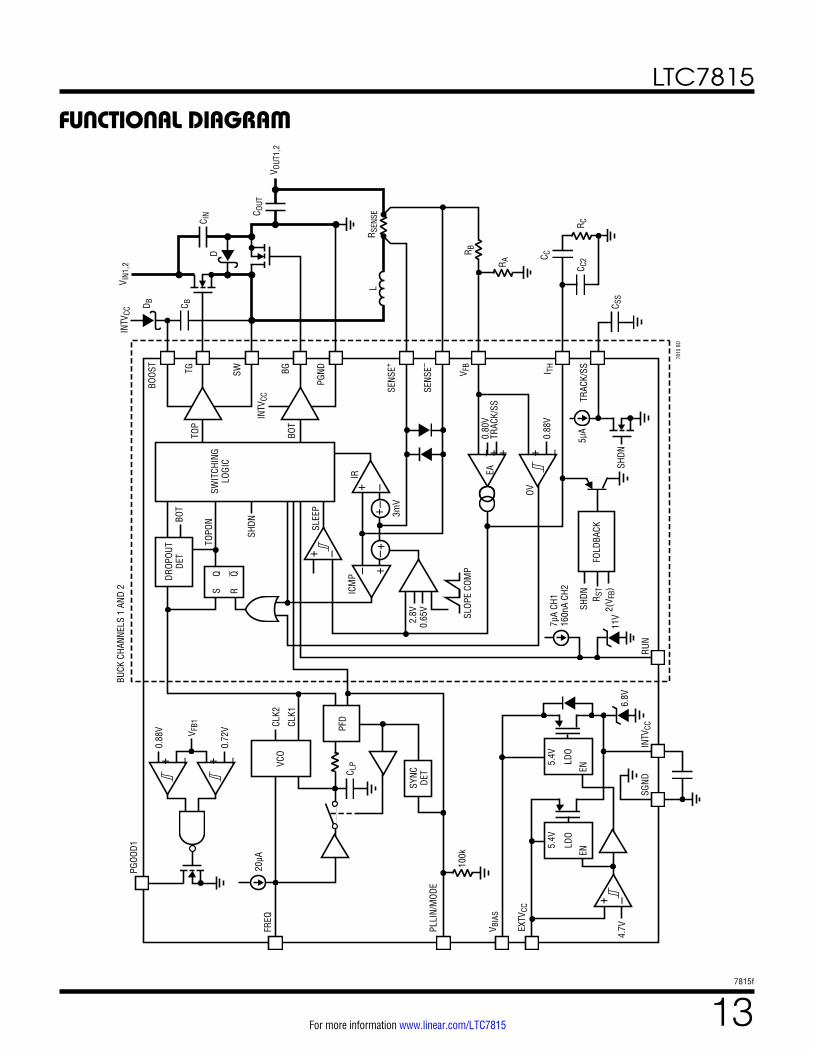
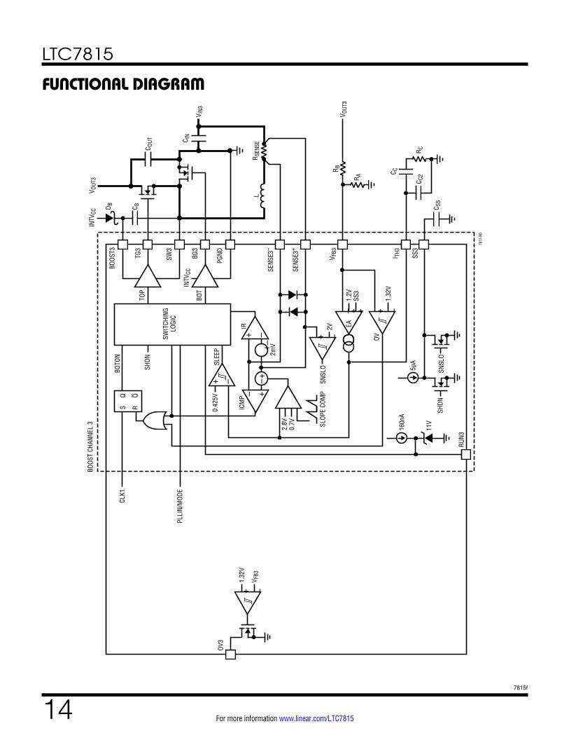
FUNCTIONAL DIAGRAM
7815
BD
SWIT
CHIN
GLO
GIC
INTV
CCV I
N1,2
D B C B
BOOS
T
TG SW BG
PGND
SENS
E+
SENS
E–
C IN
D
C OUT
INTV
CC
LR S
ENSE
TOP
BOT
DROP
OUT
DET
SQ
RQ
BOT
TOPO
N
SHDN
+ –SL
EEP
+ –
+–
+ –
+–
ICM
PIR
2.8V
0.65
V
SLOP
E CO
MP
V FB
I TH
3mV
0.80
VTR
ACK/
SS
0.88
V
+ –– ++
TRAC
K/SS
OV
C C2
R C
C C
RUN
C SS
FOLD
BACK
SHDN R S
T2(
V FB)
SHDN
7µA
CH1
160n
A CH
2
11V
PFD
VCO
C LP
CLK2
CLK1
SYNC
DET
20µA 100k
R A
R B
LDO
EN
LDO
EN
+ –4.
7V
5.4V
5.4V
INTV
CCSG
ND
EXTV
CC
V BIA
S
FREQ
PLLI
N/M
ODE
PGOO
D1
+ – + –
0.88
V
0.72
VV FB1
EA
BUCK
CHA
NNEL
S 1
AND
2
5µA
V OUT
1,2
6.8V
LTC7815
147815f
For more information www.linear.com/LTC7815
FUNCTIONAL DIAGRAM
7815
BD
SWIT
CHIN
GLO
GIC
INTV
CCV O
UT3
D B C B
BOOS
T3
TG3
SW3
BG3
PGND
SENS
E3+
SENS
E3–
C OUT C I
NIN
TVCC
LR S
ENSE
TOP
BOT
SQ
RQ
BOTO
N
SHDN
+ –SL
EEP
+ –
+–
+ –
+ –
ICM
PIR
2.8V
0.7V SL
OPE
COM
PV F
B3
I TH3
2mV
1.2V
SS3
1.32
V
+ –– ++
SS3
OV
C C2
R C
C C
RUN3
C SS
SHDN
SNSL
O
160n
A
11V
R A
R B
EA
+ –2V
SNSL
O
CLK1
PLLI
N/M
ODE
+ –
V FB3
1.32
V
OV3
0.42
5V
BOOS
T CH
ANNE
L 3
5µA
V IN3
V OUT
3
LTC7815
157815f
For more information www.linear.com/LTC7815
OPERATIONMain Control Loop
The LTC7815 uses a constant frequency, current mode step-down architecture. The two buck controllers, chan-nels 1 and 2, operate 180 degrees out of phase with each other. The boost controller, channel 3, operates in phase with channel 1. During normal operation, the external top MOSFET for the buck channels (the external bottom MOSFET for the boost channel) is turned on when the clock for that channel sets the RS latch, and is turned off when the main current comparator, ICMP, resets the RS latch. The peak inductor current at which ICMP trips and resets the latch is controlled by the voltage on the ITH pin, which is the output of the error amplifier EA. The error amplifier compares the output voltage feedback signal at the VFB pin, (which is generated with an external resis-tor divider connected across the output voltage, VOUT, to ground) to the internal 0.800V reference voltage for the bucks (1.2V reference voltage for the boost). When the load current increases, it causes a slight decrease in VFB relative to the reference, which causes the EA to increase the ITH voltage until the average inductor current matches the new load current.
After the top MOSFET for the bucks (the bottom MOSFET for the boost) is turned off each cycle, the bottom MOSFET is turned on (the top MOSFET for the boost) until either the inductor current starts to reverse, as indicated by the current comparator IR, or the beginning of the next clock cycle.
INTVCC/EXTVCC Power
Power for the top and bottom MOSFET drivers and most other internal circuitry is derived from the INTVCC pin. When the EXTVCC pin is left open or tied to a voltage less than 4.7V, the VBIAS LDO (low dropout linear regulator) supplies 5.4V from VBIAS to INTVCC. If EXTVCC is taken above 4.7V, the VBIAS LDO is turned off and an EXTVCC LDO is turned on. Once enabled, the EXTVCC LDO supplies 5.4V from EXTVCC to INTVCC. Using the EXTVCC pin allows the INTVCC power to be derived from a high efficiency external source such as one of the LTC7815 switching regulator outputs.
Each top MOSFET driver is biased from the floating boot-strap capacitor CB, which normally recharges during each
cycle through an external diode when the switch voltage goes low.
For buck channels 1 and 2, if the buck’s input voltage decreases to a voltage close to its output, the loop may enter dropout and attempt to turn on the top MOSFET continuously. The dropout detector detects this and forces the top MOSFET off for a short time every tenth cycle to allow CB to recharge resulting in about 98% duty cycle at 1MHz operation.
Shutdown and Start-Up (RUN1, RUN2, RUN3 and TRACK/SS1, TRACK/SS2, SS3 Pins)
The three channels of the LTC7815 can be independently shut down using the RUN1, RUN2 and RUN3 pins. Pulling RUN1 below 1.17V and RUN2/RUN3 below 1.20V shuts down the main control loop for that channel. Pulling all three pins below 0.7V disables all controllers and most internal circuits, including the INTVCC LDOs. In this state, the LTC7815 draws only 10µA of quiescent current.
Releasing a RUN pin allows a small internal current to pull up the pin to enable that controller. The RUN1 pin has a 7µA pull-up current while the RUN2 and RUN3 pins have a smaller 160nA. The 7µA current on RUN1 is designed to be large enough so that the RUN1 pin can be safely floated (to always enable the controller) without worry of condensation or other small board leakage pulling the pin down. This is ideal for always-on applications where one or more controllers are enabled continuously and never shut down.
Each RUN pin may also be externally pulled up or driven directly by logic. When driving a RUN pin with a low impedance source, do not exceed the absolute maximum rating of 8V. Each RUN pin has an internal 11V voltage clamp that allows the RUN pin to be connected through a resistor to a higher voltage (for example, VBIAS), so long as the maximum current in the RUN pin does not exceed 100µA.
The start-up of each channel’s output voltage VOUT is con-trolled by the voltage on the TRACK/SS pin (TRACK/SS1 for channel 1, TRACK/SS2 for channel 2, SS3 for channel 3). When the voltage on the TRACK/SS pin is less than the 0.8V internal reference for the bucks and the 1.2V internal
(Refer to Functional Diagram)
LTC7815
167815f
For more information www.linear.com/LTC7815
OPERATIONreference for the boost, the LTC7815 regulates the VFB voltage to the TRACK/SS pin voltage instead of the cor-responding reference voltage. This allows the TRACK/SS pin to be used to program a soft-start by connecting an external capacitor from the TRACK/SS pin to SGND. An internal 5µA pull-up current charges this capacitor creating a voltage ramp on the TRACK/SS pin. As the TRACK/SS voltage rises linearly from 0V to 0.8V/1.2V (and beyond up to INTVCC), the output voltage VOUT rises smoothly from zero to its final value.
Alternatively the TRACK/SS pins for buck channels 1 and 2 can be used to cause the start-up of VOUT to track that of another supply. Typically, this requires connecting to the TRACK/SS pin an external resistor divider from the other supply to ground (see the Applications Information section).
Light Load Current Operation (Burst Mode Operation, Pulse-Skipping, or Continuous Conduction) (PLLIN/MODE Pin)
The LTC7815 can be enabled to enter high efficiency Burst Mode operation, constant frequency pulse-skipping mode or forced continuous conduction mode at low load cur-rents. To select Burst Mode operation, tie the PLLIN/ MODE pin to ground. To select forced continuous opera-tion, tie the PLLIN/MODE pin to INTVCC. To select pulse-skipping mode, tie the PLLIN/MODE pin to a DC voltage greater than 1.2V and less than INTVCC – 1.3V.
When a controller is enabled for Burst Mode operation, the minimum peak current in the inductor is set to approx-imately 25% of the maximum sense voltage (30% for the boost) even though the voltage on the ITH pin indicates a lower value. If the average inductor current is higher than the load current, the error amplifier EA will decrease the voltage on the ITH pin. When the ITH voltage drops below 0.425V, the internal sleep signal goes high (enabling sleep mode) and both external MOSFETs are turned off. The ITH pin is then disconnected from the output of the EA and parked at 0.450V.
In sleep mode, much of the internal circuitry is turned off, reducing the quiescent current that the LTC7815 draws. If channel 1 is in sleep mode and the other two are shut down, the LTC7815 draws only 28µA of quiescent current. If channels 1 and 3 are in sleep mode and channel 2 is shut
down, it draws only 33µA of quiescent current. If all three controllers are enabled in sleep mode, the LTC7815 draws only 38µA of quiescent. In sleep mode, the load current is supplied by the output capacitor. As the output volt-age decreases, the EA’s output begins to rise. When the output voltage drops enough, the ITH pin is reconnected to the output of the EA, the sleep signal goes low, and the controller resumes normal operation by turning on the top external MOSFET on the next cycle of the internal oscillator.
When a controller is enabled for Burst Mode operation, the inductor current is not allowed to reverse. The reverse current comparator (IR) turns off the bottom external MOSFET (the top external MOSFET for the boost) just before the inductor current reaches zero, preventing it from reversing and going negative. Thus, the controller operates in discontinuous operation.
In forced continuous operation or clocked by an exter-nal clock source to use the phase-locked loop (see the Frequency Selection and Phase-Locked Loop section), the inductor current is allowed to reverse at light loads or under large transient conditions. The peak inductor cur-rent is determined by the voltage on the ITH pin, just as in normal operation. In this mode, the efficiency at light loads is lower than in Burst Mode operation. However, continuous operation has the advantage of lower output voltage ripple and less interference to audio circuitry. In forced continuous mode, the output ripple is independent of load current.
When the PLLIN/MODE pin is connected for pulse-skip-ping mode, the LTC7815 operates in PWM pulse-skipping mode at light loads. In this mode, constant frequency operation is maintained down to approximately 1% of designed maximum output current. At very light loads, the current comparator ICMP may remain tripped for several cycles and force the external top MOSFET to stay off for the same number of cycles (i.e., skipping pulses). The inductor current is not allowed to reverse (discontinu-ous operation). This mode, like forced continuous opera-tion, exhibits low output ripple as well as low audio noise and reduced RF interference as compared to Burst Mode operation. It provides higher low current efficiency than forced continuous mode, but not nearly as high as Burst Mode operation.
LTC7815
177815f
For more information www.linear.com/LTC7815
OPERATIONFrequency Selection and Phase-Locked Loop (FREQ and PLLIN/MODE Pins)
The selection of switching frequency is a tradeoff between efficiency and component size. Low frequency opera-tion increases efficiency by reducing MOSFET switching losses, but requires larger inductance and/or capacitance to maintain low output ripple voltage.
The switching frequency of the LTC7815’s controllers can be selected using the FREQ pin.
If the PLLIN/MODE pin is not being driven by an external clock source, the FREQ pin can be tied to SGND, tied to INTVCC, or programmed through an external resistor. Tying FREQ to SGND selects 0.94MHz while tying FREQ to INTVCC selects 1.44MHz. Placing a resistor between FREQ and SGND allows the frequency to be programmed between 0.32MHz and 2.25MHz.
A phase-locked loop (PLL) is available on the LTC7815 to synchronize the internal oscillator to an external clock source that is connected to the PLLIN/MODE pin. The LTC7815’s phase detector adjusts the voltage (through an internal lowpass filter) of the VCO input to align the turn-on of controller 1’s external top MOSFET to the ris-ing edge of the synchronizing signal. Thus, the turn-on of controller 2’s external top MOSFET is 180 degrees out of phase to the rising edge of the external clock source.
The VCO input voltage is pre-biased to the operating fre-quency set by the FREQ pin before the external clock is applied. If prebiased near the external clock frequency, the PLL loop only needs to make slight changes to the VCO input in order to synchronize the rising edge of the external clock’s to the rising edge of TG1. The ability to pre-bias the loop filter allows the PLL to lock in rapidly without deviating far from the desired frequency.
The typical capture range of the LTC7815’s phase-locked loop is from approximately 0.3MHz to 2.3MHz, with a guarantee over all manufacturing variations to be between 0.32MHz and 2.25MHz. In other words, the LTC7815’s PLL is guaranteed to lock to an external clock source whose frequency is between 0.32MHz and 2.25MHz.
The typical input clock thresholds on the PLLIN/MODE pin are 1.6V (rising) and 1.1V (falling). It is recommended
that the external clock source swings from ground (0V) to at least 2.5V.
Boost Controller Operation When VIN > VOUT
When the input voltage to the boost channel rises above its regulated VOUT voltage, the controller can behave dif-ferently depending on the mode, inductor current and VIN voltage. In forced continuous mode, the loop works to keep the top MOSFET on continuously once VIN rises above VOUT. An internal charge pump delivers current to the boost capacitor from the BOOST3 pin to maintain a sufficiently high TG voltage. (The amount of current the charge pump can deliver is characterized by two curves in the Typical Performance Characteristics section.)
In pulse-skipping mode, if VIN is between 100% and 110% of the regulated VOUT voltage, TG3 turns on if the inductor current rises above approximately 3% of the programmed ILIM current. If the part is programmed in Burst Mode operation under this same VIN window, then TG3 turns on at the same threshold current as long as the chip is awake (one of the buck channels is awake and switching). If both buck channels are asleep or shut down in this VIN window, then TG3 will remain off regardless of the inductor current.
If VIN rises above 110% of the regulated VOUT voltage in any mode, the controller turns on TG3 regardless of the inductor current. In Burst Mode operation, however, the internal charge pump turns off if the entire chip is asleep (the two buck channels are asleep or shut down). With the charge pump off, there would be nothing to prevent the boost capacitor from discharging, resulting in an insufficient TG voltage needed to keep the top MOSFET completely on. The charge pump turns back on when the chip wakes up, and it remains on as long as one of the buck channels is actively switching.
Boost Controller at Low SENSE Pin Common Voltage
The current comparator of the boost controller is powered directly from the SENSE3+ pin and can operate to volt-ages as low as 2.5V. Since this is lower than the VBIAS UVLO of the chip, VBIAS can be connected to the output of the boost controller, as illustrated in the typical applica-tion circuit in Figure 9. This allows the boost controller to
LTC7815
187815f
For more information www.linear.com/LTC7815
handle input voltage transients down to 2.5V while main-taining output voltage regulation. If the SENSE3+ rises back above 2.5V, the SS3 pin will be released initiating a new soft-start sequence.
Buck Controller Output Overvoltage Protection
The two buck channels have an overvoltage compara-tor that guards against transient overshoots as well as other more serious conditions that may overvoltage their outputs. When the VFB1,2 pin rises by more than 10% above its regulation point of 0.800V, the top MOSFET is turned off and the bottom MOSFET is turned on until the overvoltage condition is cleared.
Channel 1 Power Good (PGOOD1)
Channel 1 has a PGOOD1 pin that is connected to an open drain of an internal N-channel MOSFET. The MOSFET turns on and pulls the PGOOD1 pin low when the VFB1 pin voltage is not within ±10% of the 0.8V reference voltage for the buck channel. The PGOOD1 pin is also pulled low when the RUN1 pin is low (shut down). When the VFB1 pin voltage is within the ±10% requirement, the MOSFET is turned off and the pin is allowed to be pulled up by an external resistor to a source no greater than 6V.
Boost Overvoltage Indicator (OV3)
The OV3 pin is an overvoltage indicator that signals whether the output voltage of the channel 3 boost con-troller goes over its programmed regulated voltage. The pin is connected to an open drain of an internal N-channel MOSFET. The MOSFET turns on and pulls the OV3 pin low when the VFB3 pin voltage is less than 110% of the 1.2V reference voltage for the boost channel. The OV3 pin is also pulled low when the RUN3 pin is low (shut down). When the VFB3 pin voltage goes higher than 110% of the 1.2V reference, the MOSFET is turned off and the pin is allowed to be pulled up by an external resistor to a source no greater than 6V.
Buck Foldback Current
When the buck output voltage falls to less than 70% of its nominal level, foldback current limiting is activated, pro-gressively lowering the peak current limit in proportion to the severity of the overcurrent or short-circuit condition. Foldback current limiting is disabled during the soft-start interval (as long as the VFB voltage is keeping up with the TRACK/SS1,2 voltage). There is no foldback current limiting for the boost channel.
OPERATION
LTC7815
197815f
For more information www.linear.com/LTC7815
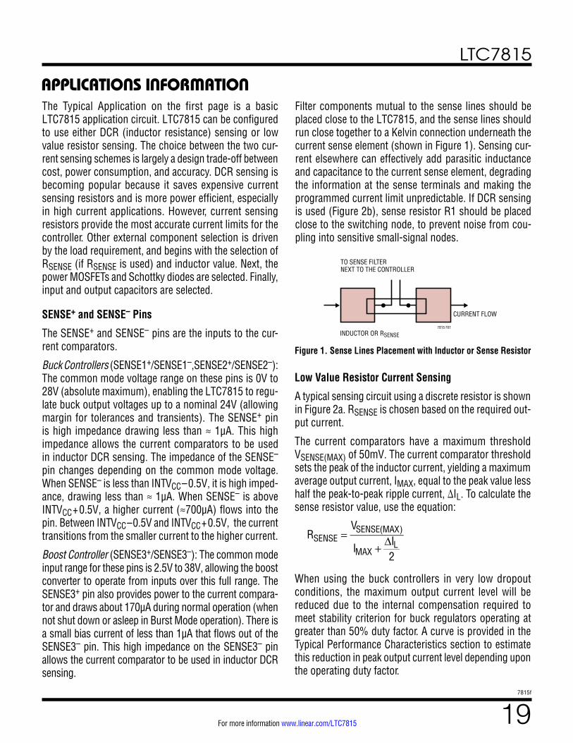
Figure 1. Sense Lines Placement with Inductor or Sense Resistor
APPLICATIONS INFORMATIONThe Typical Application on the first page is a basic LTC7815 application circuit. LTC7815 can be configured to use either DCR (inductor resistance) sensing or low value resistor sensing. The choice between the two cur-rent sensing schemes is largely a design trade-off between cost, power consumption, and accuracy. DCR sensing is becoming popular because it saves expensive current sensing resistors and is more power efficient, especially in high current applications. However, current sensing resistors provide the most accurate current limits for the controller. Other external component selection is driven by the load requirement, and begins with the selection of RSENSE (if RSENSE is used) and inductor value. Next, the power MOSFETs and Schottky diodes are selected. Finally, input and output capacitors are selected.
SENSE+ and SENSE– Pins
The SENSE+ and SENSE– pins are the inputs to the cur-rent comparators.
Buck Controllers (SENSE1+/SENSE1–,SENSE2+/SENSE2–): The common mode voltage range on these pins is 0V to 28V (absolute maximum), enabling the LTC7815 to regu-late buck output voltages up to a nominal 24V (allowing margin for tolerances and transients). The SENSE+ pin is high impedance drawing less than ≈ 1µA. This high impedance allows the current comparators to be used in inductor DCR sensing. The impedance of the SENSE– pin changes depending on the common mode voltage. When SENSE– is less than INTVCC–0.5V, it is high imped-ance, drawing less than ≈ 1µA. When SENSE– is above INTVCC+0.5V, a higher current (≈700µA) flows into the pin. Between INTVCC–0.5V and INTVCC+0.5V, the current transitions from the smaller current to the higher current.
Boost Controller (SENSE3+/SENSE3–): The common mode input range for these pins is 2.5V to 38V, allowing the boost converter to operate from inputs over this full range. The SENSE3+ pin also provides power to the current compara-tor and draws about 170µA during normal operation (when not shut down or asleep in Burst Mode operation). There is a small bias current of less than 1µA that flows out of the SENSE3– pin. This high impedance on the SENSE3– pin allows the current comparator to be used in inductor DCR sensing.
Filter components mutual to the sense lines should be placed close to the LTC7815, and the sense lines should run close together to a Kelvin connection underneath the current sense element (shown in Figure 1). Sensing cur-rent elsewhere can effectively add parasitic inductance and capacitance to the current sense element, degrading the information at the sense terminals and making the programmed current limit unpredictable. If DCR sensing is used (Figure 2b), sense resistor R1 should be placed close to the switching node, to prevent noise from cou-pling into sensitive small-signal nodes.
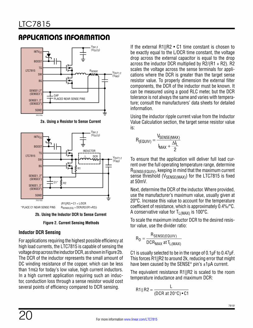
Low Value Resistor Current Sensing
A typical sensing circuit using a discrete resistor is shown in Figure 2a. RSENSE is chosen based on the required out-put current.
The current comparators have a maximum threshold VSENSE(MAX) of 50mV. The current comparator threshold sets the peak of the inductor current, yielding a maximum average output current, IMAX, equal to the peak value less half the peak-to-peak ripple current, ∆IL. To calculate the sense resistor value, use the equation:
RSENSE =VSENSE(MAX)
IMAX + ΔIL2
When using the buck controllers in very low dropout conditions, the maximum output current level will be reduced due to the internal compensation required to meet stability criterion for buck regulators operating at greater than 50% duty factor. A curve is provided in the Typical Performance Characteristics section to estimate this reduction in peak output current level depending upon the operating duty factor.
7815 F01
TO SENSE FILTERNEXT TO THE CONTROLLER
INDUCTOR OR RSENSE
CURRENT FLOW
LTC7815
207815f
For more information www.linear.com/LTC7815
APPLICATIONS INFORMATION
Inductor DCR Sensing
For applications requiring the highest possible efficiency at high load currents, the LTC7815 is capable of sensing the voltage drop across the inductor DCR, as shown in Figure 2b. The DCR of the inductor represents the small amount of DC winding resistance of the copper, which can be less than 1mΩ for today’s low value, high current inductors. In a high current application requiring such an induc-tor, conduction loss through a sense resistor would cost several points of efficiency compared to DCR sensing.
If the external R1||R2 • C1 time constant is chosen to be exactly equal to the L/DCR time constant, the voltage drop across the external capacitor is equal to the drop across the inductor DCR multiplied by R2/(R1 + R2). R2 scales the voltage across the sense terminals for appli-cations where the DCR is greater than the target sense resistor value. To properly dimension the external filter components, the DCR of the inductor must be known. It can be measured using a good RLC meter, but the DCR tolerance is not always the same and varies with tempera-ture; consult the manufacturers’ data sheets for detailed information.
Using the inductor ripple current value from the Inductor Value Calculation section, the target sense resistor value is:
R(EQUIV) =VSENSE(MAX)
IMAX + ΔIL2
To ensure that the application will deliver full load cur-rent over the full operating temperature range, determine RSENSE(EQUIV), keeping in mind that the maximum current sense threshold (VSENSE(MAX)) for the LTC7815 is fixed at 50mV.
Next, determine the DCR of the inductor. Where provided, use the manufacturer’s maximum value, usually given at 20°C. Increase this value to account for the temperature coefficient of resistance, which is approximately 0.4%/°C. A conservative value for TL(MAX) is 100°C.
To scale the maximum inductor DCR to the desired resis-tor value, use the divider ratio:
RD =
RSENSE(EQUIV)
DCRMAX at TL(MAX)
C1 is usually selected to be in the range of 0.1µF to 0.47µF. This forces R1||R2 to around 2k, reducing error that might have been caused by the SENSE+ pin’s ±1µA current.
The equivalent resistance R1||R2 is scaled to the room temperature inductance and maximum DCR:
R1R2 =
L(DCR at 20°C) • C1
2b. Using the Inductor DCR to Sense Current
2a. Using a Resistor to Sense Current
Figure 2. Current Sensing Methods
7815 F02a
LTC7815
INTVCC
BOOST
TG
SW
BG
SENSE1,2+
(SENSE3–)
SENSE1, 2–
(SENSE3+)
SGND
VIN1,2(VOUT3)
VOUT1,2(VIN3)
RSENSE
CAPPLACED NEAR SENSE PINS
7815 F02b
LTC7815
INTVCC
BOOST
TG
SW
BG
SENSE1, 2+
(SENSE3–)
SENSE1, 2–
(SENSE3+)
SGND
VIN1,2(VOUT3)
VOUT1,2(VIN3)
C1* R2
*PLACE C1 NEAR SENSE PINS RSENSE(EQ) = DCR(R2/(R1+R2))
L DCR
INDUCTOR
R1
(R1||R2) • C1 = L/DCR

LTC7815
217815f
For more information www.linear.com/LTC7815
APPLICATIONS INFORMATIONThe sense resistor values are:
R1= R1!R2
RD; R2 = R1•RD
1−RD
The maximum power loss in R1 is related to duty cycle. For the buck controllers, the maximum power loss will occur in continuous mode at the maximum input voltage:
PLOSS R1=
(VIN(MAX) − VOUT) • VOUT
R1
For the boost controller, the maximum power loss in R1 will occur in continuous mode at VIN = 1/2•VOUT:
PLOSS R1=
(VOUT(MAX) − VIN) • VIN
R1
Ensure that R1 has a power rating higher than this value. If high efficiency is necessary at light loads, consider this power loss when deciding whether to use DCR sensing or sense resistors. Light load power loss can be mod-estly higher with a DCR network than with a sense resis-tor, due to the extra switching losses incurred through R1. However, DCR sensing eliminates a sense resistor, reduces conduction losses and provides higher efficiency at heavy loads. Peak efficiency is about the same with either method.
Inductor Value Calculation
The operating frequency and inductor selection are inter-related in that higher operating frequencies allow the use of smaller inductor and capacitor values. So why would anyone ever choose to operate at lower frequencies with larger components? The answer is efficiency. A higher frequency generally results in lower efficiency because of MOSFET gate charge losses. In addition to this basic trade-off, the effect of inductor value on ripple current and low current operation must also be considered.
The inductor value has a direct effect on ripple current. The inductor ripple current ∆IL decreases with higher
inductance or frequency. For the buck controllers, ∆IL increases with higher VIN:
ΔIL = 1
(f)(L)VOUT 1−
VOUTVIN
⎛⎝⎜
⎞⎠⎟
For the boost controller, the inductor ripple current ∆IL increases with higher VOUT:
ΔIL = 1
(f)(L)VIN 1− VIN
VOUT
⎛⎝⎜
⎞⎠⎟
Accepting larger values of ∆IL allows the use of low induc-tances, but results in higher output voltage ripple and greater core losses. A reasonable starting point for set-ting ripple current is ∆IL = 0.3(IMAX). The maximum ∆IL occurs at the maximum input voltage for the bucks and VIN = 1/2•VOUT for the boost.
The inductor value also has secondary effects. The tran-sition to Burst Mode operation begins when the average inductor current required results in a peak current below 25% of the current limit (30% for the boost) determined by RSENSE. Lower inductor values (higher ∆IL) will cause this to occur at lower load currents, which can cause a dip in efficiency in the upper range of low current operation. In Burst Mode operation, lower inductance values will cause the burst frequency to decrease.
Inductor Core Selection
Once the value for L is known, the type of inductor must be selected. High efficiency converters generally cannot afford the core loss found in low cost powdered iron cores, forcing the use of more expensive ferrite or molypermal-loy cores. Actual core loss is independent of core size for a fixed inductor value, but it is very dependent on induc-tance selected. As inductance increases, core losses go down. Unfortunately, increased inductance requires more turns of wire and therefore copper losses will increase.
Ferrite designs have very low core loss and are preferred at high switching frequencies, so design goals can con-centrate on copper loss and preventing saturation. Ferrite
LTC7815
227815f
For more information www.linear.com/LTC7815
APPLICATIONS INFORMATIONcore material saturates “hard,” which means that induc-tance collapses abruptly when the peak design current is exceeded. This results in an abrupt increase in inductor ripple current and consequent output voltage ripple. Do not allow the core to saturate!
Power MOSFET and Schottky Diode (Optional) Selection
Two external power MOSFETs must be selected for each controller in the LTC7815: one N-channel MOSFET for the top switch (main switch for the buck, synchronous for the boost), and one N-channel MOSFET for the bottom switch (main switch for the boost, synchronous for the buck).
The peak-to-peak drive levels are set by the INTVCC voltage. This voltage is typically 5.4V during start-up (see EXTVCC Pin Connection). Consequently, logic-level threshold MOSFETs must be used in most applications. Pay close attention to the BVDSS specification for the MOSFETs as well; many of the logic level MOSFETs are limited to 30V or less.
Selection criteria for the power MOSFETs include the on-resistance RDS(ON), Miller capacitance CMILLER, input voltage and maximum output current. Miller capacitance, CMILLER, can be approximated from the gate charge curve usually provided on the MOSFET manufacturers’ data sheet. CMILLER is equal to the increase in gate charge along the horizontal axis while the curve is approximately flat divided by the specified change in VDS. This result is then multiplied by the ratio of the application applied VDS to the gate charge curve specified VDS. When the IC is operating in continuous mode the duty cycles for the top and bottom MOSFETs are given by:
Buck Main Switch Duty Cycle =VOUTVIN
Buck Sync Switch Duty Cycle =VIN − VOUT
VIN
Boost Main Switch Duty Cycle =VOUT − VIN
VOUT
Boost Sync Switch Duty Cycle = VINVOUT
The MOSFET power dissipations at maximum output cur-rent are given by:
PMAIN_BUCK =VOUTVIN
IOUT(MAX)( )2 1+ δ( )RDS(ON) +
(VIN)2IOUT(MAX)
2⎛⎝⎜
⎞⎠⎟
(RDR)(CMILLER) •
1VINTVCC − VTHMIN
+ 1VTHMIN
⎡
⎣⎢
⎤
⎦⎥(f)
PSYNC_BUCK =VIN − VOUT
VINIOUT(MAX)( )2 1+ δ( )RDS(ON)
PMAIN_BOOST =VOUT − VIN( )VOUT
VIN2 IOUT(MAX)( )2 •
1+ δ( )RDS(ON) +V 3
OUTVIN
⎛
⎝⎜
⎞
⎠⎟
IOUT(MAX)
2⎛⎝⎜
⎞⎠⎟
•
RDR( ) CMILLER( ) •1
VINTVCC − VTHMIN+ 1
VTHMIN
⎡
⎣⎢
⎤
⎦⎥(f)
PSYNC_BOOST = VINVOUT
IOUT(MAX)( )2 1+ δ( )RDS(ON)
where z is the temperature dependency of RDS(ON) and RDR (approximately 2Ω) is the effective driver resistance at the MOSFET’s Miller threshold voltage. VTHMIN is the typical MOSFET minimum threshold voltage.
Both MOSFETs have I2R losses while the main N-channel equations for the buck and boost controllers include an additional term for transition losses, which are highest at high input voltages for the bucks and low input volt-ages for the boost. For VIN < 20V (high VIN for the boost) the high current efficiency generally improves with larger MOSFETs, while for VIN > 20V (low VIN for the boost) the transition losses rapidly increase to the point that the use of a higher RDS(ON) device with lower CMILLER actually
LTC7815
237815f
For more information www.linear.com/LTC7815
APPLICATIONS INFORMATIONprovides higher efficiency. The synchronous MOSFET losses for the buck controllers are greatest at high input voltage when the top switch duty factor is low or during a short-circuit when the synchronous switch is on close to 100% of the period. The synchronous MOSFET losses for the boost controller are greatest when the input voltage approaches the output voltage or during an overvoltage event when the synchronous switch is on 100% of the period.
The term (1+ z) is generally given for a MOSFET in the form of a normalized RDS(ON) vs Temperature curve, but z = 0.005/°C can be used as an approximation for low voltage MOSFETs.
A Schottky diode can be inserted in parallel with the synchronous MOSFET to conduct during the dead-time between the conduction of the two power MOSFETs. This prevents the body diode of the synchronous MOSFET from turning on, storing charge during the dead-time and requiring a reverse recovery period that could cost as much as 3% in efficiency at high VIN. A 1A to 3A Schottky is generally a good compromise for both regions of opera-tion due to the relatively small average current. Larger diodes result in additional transition losses due to their larger junction capacitance.
Boost CIN, COUT Selection
The input ripple current in a boost converter is relatively low (compared with the output ripple current), because this current is continuous. The boost input capacitor CIN voltage rating should comfortably exceed the maximum input voltage. Although ceramic capacitors can be rela-tively tolerant of overvoltage conditions, aluminum elec-trolytic capacitors are not. Be sure to characterize the input voltage for any possible overvoltage transients that could apply excess stress to the input capacitors.
The value of CIN is a function of the source impedance, and in general, the higher the source impedance, the higher the required input capacitance. The required amount of input capacitance is also greatly affected by the duty cycle. High output current applications that also experience high
duty cycles can place great demands on the input supply, both in terms of DC current and ripple current.
In a boost converter, the output has a discontinuous cur-rent, so COUT must be capable of reducing the output voltage ripple. The effects of ESR (equivalent series resis-tance) and the bulk capacitance must be considered when choosing the right capacitor for a given output ripple volt-age. The steady ripple due to charging and discharging the bulk capacitance is given by:
Ripple =
IOUT(MAX) • VOUT − VIN(MIN)( )COUT • VOUT • f
V
where COUT is the output filter capacitor.
The steady ripple due to the voltage drop across the ESR is given by:
∆VESR = IL(MAX) • ESR
Multiple capacitors placed in parallel may be needed to meet the ESR and RMS current handling requirements. Dry tantalum, special polymer, aluminum electrolytic and ceramic capacitors are all available in surface mount packages. Ceramic capacitors have excellent low ESR characteristics but can have a high voltage coefficient. Capacitors are now available with low ESR and high ripple current ratings such as OS-CON and POSCAP.
Buck CIN, COUT Selection
The selection of CIN for the two buck controllers is sim-plified by the 2-phase architecture and its impact on the worst-case RMS current drawn through the input net-work (battery/fuse/capacitor). It can be shown that the worst-case capacitor RMS current occurs when only one controller is operating. The controller with the highest (VOUT)(IOUT) product needs to be used in the formula shown in Equation (1) to determine the maximum RMS capacitor current requirement. Increasing the output cur-rent drawn from the other controller will actually decrease the input RMS ripple current from its maximum value. The out-of-phase technique typically reduces the input
LTC7815
247815f
For more information www.linear.com/LTC7815
APPLICATIONS INFORMATIONcapacitor’s RMS ripple current by a factor of 30% to 70% when compared to a single phase power supply solution.
In continuous mode, the source current of the top MOSFET is a square wave of duty cycle (VOUT)/(VIN). To prevent large voltage transients, a low ESR capacitor sized for the maximum RMS current of one channel must be used. The maximum RMS capacitor current is given by:
CIN Required IRMS ≈IMAX
VINVOUT( ) VIN − VOUT( )⎡⎣ ⎤⎦
1/2
(1)
This formula has a maximum at VIN = 2VOUT, where IRMS = IOUT/2. This simple worst-case condition is commonly used for design because even significant deviations do not offer much relief. Note that capacitor manufacturers’ ripple current ratings are often based on only 2000 hours of life. This makes it advisable to further derate the capaci-tor, or to choose a capacitor rated at a higher temperature than required. Several capacitors may be paralleled to meet size or height requirements in the design. Due to the high operating frequency of the LTC7815, ceramic capacitors can also be used for CIN. Always consult the manufacturer if there is any question.
The benefit of the LTC7815 2-phase operation can be calculated by using Equation (1) for the higher power controller and then calculating the loss that would have resulted if both controller channels switched on at the same time. The total RMS power lost is lower when both controllers are operating due to the reduced overlap of current pulses required through the input capacitor’s ESR. This is why the input capacitor’s requirement cal-culated above for the worst-case controller is adequate for the dual controller design. Also, the input protection fuse resistance, battery resistance, and PC board trace resistance losses are also reduced due to the reduced peak currents in a 2-phase system. The overall benefit of a multiphase design will only be fully realized when the source impedance of the power supply/battery is included in the efficiency testing. The drains of the top MOSFETs should be placed within 1cm of each other and share a common CIN (s). Separating the drains and CIN may pro-duce undesirable voltage and current resonances at VIN.
A small (0.1µF to 1µF) bypass capacitor between the chip VIN pin and ground, placed close to the LTC7815, is also
suggested. A small (1Ω to 10Ω) resistor placed between CIN (C1) and the VIN pin provides further isolation between the two channels.
The selection of COUT is driven by the effective series resistance (ESR). Typically, once the ESR requirement is satisfied, the capacitance is adequate for filtering. The output ripple (∆VOUT) is approximated by:
ΔVOUT ≈ ΔIL ESR+ 1
8fCOUT
⎛⎝⎜
⎞⎠⎟
where f is the operating frequency, COUT is the output capacitance and ∆IL is the ripple current in the inductor. The output ripple is highest at maximum input voltage since ∆IL increases with input voltage.
Setting Output Voltage
The LTC7815 output voltages are each set by an external feedback resistor divider carefully placed across the out-put, as shown in Figure 3. The regulated output voltages are determined by:
VOUT, BUCK = 0.8V 1+ RBRA
⎛⎝⎜
⎞⎠⎟
VOUT,BOOST = 1.2V 1+ RBRA
⎛⎝⎜
⎞⎠⎟
To improve the frequency response, a feedforward capaci-tor, CFF, may be used. Great care should be taken to route the VFB line away from noise sources, such as the inductor or the SW line.
Figure 3. Setting Output Voltage
7815 F03
1/3 LTC7815
VFB
RB CFF
RA
VOUT
LTC7815
257815f
For more information www.linear.com/LTC7815
APPLICATIONS INFORMATIONTracking and Soft-Start (TRACK/SS1, TRACK/SS2, SS3 Pins)
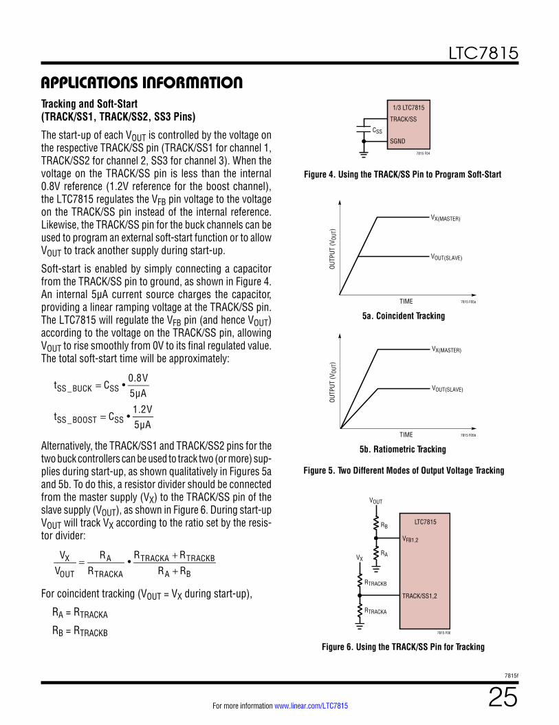
The start-up of each VOUT is controlled by the voltage on the respective TRACK/SS pin (TRACK/SS1 for channel 1, TRACK/SS2 for channel 2, SS3 for channel 3). When the voltage on the TRACK/SS pin is less than the internal 0.8V reference (1.2V reference for the boost channel), the LTC7815 regulates the VFB pin voltage to the voltage on the TRACK/SS pin instead of the internal reference. Likewise, the TRACK/SS pin for the buck channels can be used to program an external soft-start function or to allow VOUT to track another supply during start-up.
Soft-start is enabled by simply connecting a capacitor from the TRACK/SS pin to ground, as shown in Figure 4. An internal 5µA current source charges the capacitor, providing a linear ramping voltage at the TRACK/SS pin. The LTC7815 will regulate the VFB pin (and hence VOUT) according to the voltage on the TRACK/SS pin, allowing VOUT to rise smoothly from 0V to its final regulated value. The total soft-start time will be approximately:
tSS _BUCK = CSS •0.8V5µA
tSS _BOOST = CSS •1.2V5µA
Alternatively, the TRACK/SS1 and TRACK/SS2 pins for the two buck controllers can be used to track two (or more) sup-plies during start-up, as shown qualitatively in Figures 5a and 5b. To do this, a resistor divider should be connected from the master supply (VX) to the TRACK/SS pin of the slave supply (VOUT), as shown in Figure 6. During start-up VOUT will track VX according to the ratio set by the resis-tor divider:
VX
VOUT=
RA
RTRACKA•
RTRACKA + RTRACKB
RA + RB
For coincident tracking (VOUT = VX during start-up),
RA = RTRACKA
RB = RTRACKB
5a. Coincident Tracking
5b. Ratiometric Tracking
Figure 5. Two Different Modes of Output Voltage Tracking
Figure 6. Using the TRACK/SS Pin for Tracking
7815 F05a
VX(MASTER)
VOUT(SLAVE)
OUTP
UT (V
OUT)
TIME
7815 F05b
VX(MASTER)
VOUT(SLAVE)
OUTP
UT (V
OUT)
TIME
7815 F06
LTC7815
VFB1,2
TRACK/SS1,2
RB
RA
VOUT
RTRACKB
RTRACKA
VX
Figure 4. Using the TRACK/SS Pin to Program Soft-Start
7815 F04
1/3 LTC7815
TRACK/SS
SGND
CSS
LTC7815
267815f
For more information www.linear.com/LTC7815
APPLICATIONS INFORMATIONINTVCC Regulators
The LTC7815 features two separate internal P-channel low dropout linear regulators (LDO) that supply power at the INTVCC pin from either the VBIAS supply pin or the EXTVCC pin depending on the connection of the EXTVCC pin. INTVCC powers the gate drivers and much of the LTC7815’s internal circuitry. The VBIAS LDO and the EXTVCC LDO regulate INTVCC to 5.4V. Each of these must be bypassed to ground with a minimum of 4.7µF ceramic capacitor. No matter what type of bulk capacitor is used, an additional 1µF ceramic capacitor placed directly adjacent to the INTVCC and PGND IC pins is highly recom-mended. Good bypassing is needed to supply the high transient currents required by the MOSFET gate drivers and to prevent interaction between the channels.
High input voltage applications in which large MOSFETs are being driven at high frequencies may cause the maxi-mum junction temperature rating for the LTC7815 to be exceeded. The INTVCC current, which is dominated by the gate charge current, may be supplied by either the VBIAS LDO or the EXTVCC LDO. When the voltage on the EXTVCC pin is less than 4.7V, the VBIAS LDO is enabled. Power dissipation for the IC in this case is highest and is equal to VBIAS • IINTVCC. The gate charge current is dependent on operating frequency as discussed in the Efficiency Considerations section. The junction temperature can be estimated by using the equations given in Note 2 of the Electrical Characteristics. For example, the LTC7815 INTVCC current is limited to less than 40mA from a 40V supply when not using the EXTVCC supply at a 70°C ambi-ent temperature:
TJ = 70°C + (40mA)(40V)(34.7°C/W) = 125°C
To prevent the maximum junction temperature from being exceeded, the input supply current must be checked while operating in continuous conduction mode (PLLIN/MODE = INTVCC) at maximum VIN.
When the voltage applied to EXTVCC rises above 4.7V, the VBIAS LDO is turned off and the EXTVCC LDO is enabled. The EXTVCC LDO remains on as long as the voltage applied to EXTVCC remains above 4.5V. The EXTVCC LDO attempts to regulate the INTVCC voltage to 5.4V, so while EXTVCC is less than 5.4V, the LDO is in dropout and the INTVCC
voltage is approximately equal to EXTVCC. When EXTVCC is greater than 5.4V, up to an absolute maximum of 14V, INTVCC is regulated to 5.4V.
Using the EXTVCC LDO allows the MOSFET driver and control power to be derived from one of the LTC7815’s switching regulator outputs (4.7V ≤ VOUT ≤ 14V) during normal operation and from the VBIAS LDO when the output is out of regulation (e.g., start-up, short-circuit). If more current is required through the EXTVCC LDO than is speci-fied, an external Schottky diode can be added between the EXTVCC and INTVCC pins. In this case, do not apply more than 6V to the EXTVCC pin and make sure that EXTVCC ≤ VBIAS.
Significant efficiency and thermal gains can be realized by powering INTVCC from the buck output, since the VIN current resulting from the driver and control currents will be scaled by a factor of (Duty Cycle)/(Switcher Efficiency). For 5V to 14V regulator outputs, this means connecting the EXTVCC pin directly to VOUT. Tying the EXTVCC pin to a 8.5V supply reduces the junction temperature in the previous example from 125°C to:
TJ = 70°C + (40mA)(8.5V)(34.7°C/W) = 82°C
However, for 3.3V and other low voltage outputs, addi-tional circuitry is required to derive INTVCC power from the output.
The following list summarizes the three possible connec-tions for EXTVCC:
1. EXTVCC grounded. This will cause INTVCC to be pow-ered from the internal 5.4V regulator resulting in an efficiency penalty of up to 10% at high input voltages.
2. EXTVCC connected directly to the output voltage of one of the buck regulators. This is the normal connection for a 5V to 14V regulator and provides the highest efficiency.
3. EXTVCC connected to an external supply. If an exter-nal supply is available in the 5V to 14V range, it may be used to power EXTVCC providing it is compatible with the MOSFET gate drive requirements. Ensure that EXTVCC ≤ VBIAS.
LTC7815
277815f
For more information www.linear.com/LTC7815
APPLICATIONS INFORMATIONTopside MOSFET Driver Supply (CB, DB)
External bootstrap capacitors CB connected to the BOOST pins supply the gate drive voltages for the top-side MOSFETs. Capacitor CB in the Functional Diagram is charged though external diode DB from INTVCC when the SW pin is low. When one of the topside MOSFETs is to be turned on, the driver places the CB voltage across the gate-source of the desired MOSFET. This enhances the MOSFET and turns on the topside switch. The switch node voltage, SW, rises to VIN for the buck channels (VOUT for the boost channel) and the BOOST pin follows. With the topside MOSFET on, the boost voltage is above the input supply: VBOOST = VIN + VINTVCC (VBOOST = VOUT + VINTVCC for the boost controller). The value of the boost capacitor CB needs to be 100 times that of the total input capacitance of the topside MOSFET(s). The reverse breakdown of the external Schottky diode must be greater than VIN(MAX) for the buck channels and VOUT(MAX) for the boost channel.
The external diode DB can be a Schottky diode or silicon diode, but in either case it should have low leakage and fast recovery. Pay close attention to the reverse leak-age at high temperatures where it generally increases substantially.
The topside MOSFET driver for the boost channel includes an internal charge pump that delivers current to the boot-strap capacitor from the BOOST3 pin. This charge cur-rent maintains the bias voltage required to keep the top MOSFET on continuously during dropout/overvoltage conditions. The Schottky/silicon diode selected for the boost topside driver should have a reverse leakage less than the available output current the charge pump can supply. Curves displaying the available charge pump cur-rent under different operating conditions can be found in the Typical Performance Characteristics section.
A leaky diode DB in the boost converter can not only pre-vent the top MOSFET from fully turning on but it can also completely discharge the bootstrap capacitor CB and cre-ate a current path from the input voltage to the BOOST3 pin to INTVCC. This can cause INTVCC to rise if the diode leakage exceeds the current consumption on INTVCC. This is particularly a concern in Burst Mode operation where the load on INTVCC can be very small. There is an internal voltage clamp on INTVCC that prevents the INTVCC voltage from running away, but this clamp should
be regarded as a failsafe only. The external Schottky or silicon diode should be carefully chosen such that INTVCC never gets charged up much higher than its normal regu-lation voltage.
Care should also be taken when choosing the external diode DB for the buck converters. A leaky diode not only increases the quiescent current of the buck converter, but it can also cause a similar leakage path to INTVCC from VOUT for applications with output voltages greater than the INTVCC voltage (~5.4V).
Fault Conditions: Buck Current Limit and Current Foldback
The LTC7815 includes current foldback for the buck channels to help limit load current when the output is shorted to ground. If the buck output falls below 70% of its nominal output level, then the maximum sense volt-age is progressively lowered from 100% to 40% of its maximum selected value. Under short-circuit conditions with very low duty cycles, the buck channel will begin cycle skipping in order to limit the short-circuit current. In this situation the bottom MOSFET will be dissipating most of the power but less than in normal operation. The short-circuit ripple current is determined by the minimum on-time tON(MIN) of the LTC7815 (≈40ns), the input volt-age and inductor value:
∆IL(SC) = tON(MIN) (VIN/L)
The resulting average short-circuit current is:
ISC = 40% •ILIM(MAX) −12ΔIL(SC)
Fault Conditions: Buck Overvoltage Protection (Crowbar)
The overvoltage crowbar is designed to blow a system input fuse when the output voltage of the one of the buck regulators rises much higher than nominal levels. The crowbar causes huge currents to flow, that blow the fuse to protect against a shorted top MOSFET if the short occurs while the controller is operating.
A comparator monitors the buck output for overvoltage conditions. The comparator detects faults greater than 10% above the nominal output voltage. When this condi-tion is sensed, the top MOSFET of the buck controller is
LTC7815
287815f
For more information www.linear.com/LTC7815
APPLICATIONS INFORMATIONturned off and the bottom MOSFET is turned on until the overvoltage condition is cleared. The bottom MOSFET remains on continuously for as long as the overvoltage condition persists; if VOUT returns to a safe level, normal operation automatically resumes.
A shorted top MOSFET for the buck channel will result in a high current condition which will open the system fuse. The switching regulator will regulate properly with a leaky top MOSFET by altering the duty cycle to accommodate the leakage.
Fault Conditions: Over Temperature Protection
At higher temperatures, or in cases where the internal power dissipation causes excessive self heating on chip (such as INTVCC short to ground), the over temperature shutdown circuitry will shut down the LTC7815. When the junction temperature exceeds approximately 170°C, the over temperature circuitry disables the INTVCC LDO, caus-ing the INTVCC supply to collapse and effectively shutting down the entire LTC7815 chip. Once the junction tem-perature drops back to approximately 155°C, the INTVCC LDO turns back on. Long term overstress (TJ > 125°C) should be avoided as it can degrade the performance or shorten the life of the part.
Frequency Synchronization and Selection
The LTC7815 has an internal phase-locked loop (PLL) comprised of a phase frequency detector, a lowpass filter, and a voltage-controlled oscillator (VCO). This allows the turn-on of the top MOSFET of controller 1 to be locked to the rising edge of an external clock signal applied to the PLLIN/MODE pin. The turn-on of controller 2’s top MOSFET is thus 180 degrees out of phase with the exter-nal clock. The phase detector is an edge sensitive digital type that provides zero degrees phase shift between the external and internal oscillators. This type of phase detec-tor does not exhibit false lock to harmonics of the external clock.
If the external clock frequency is greater than the internal oscillator’s frequency, fOSC, then current is sourced con-tinuously from the phase detector output, pulling up the VCO input. When the external clock frequency is less than fOSC, current is sunk continuously, pulling down the VCO input. If the external and internal frequencies are the same but exhibit a phase difference, the current sources turn on for an amount of time corresponding to the phase dif-ference. The voltage at the VCO input is adjusted until the phase and frequency of the internal and external oscilla-tors are identical. At the stable operating point, the phase detector output is high impedance and the internal filter capacitor, CLP, holds the voltage at the VCO input.
Note that the LTC7815 can only be synchronized to an external clock whose frequency is within range of the LTC7815’s internal VCO, which is guaranteed to be between 0.32MHz to 2.25MHz.
Typically, the external clock (on PLLIN/MODE pin) input high threshold is 1.6V, while the input low threshold is 1.1V. The LTC7815 is guaranteed to synchronize to an external clock that swings up to at least 2.5V and down to 0.5V or less.
Rapid phase-locking can be achieved by using the FREQ pin to set a free-running frequency near the desired syn-chronization frequency. The VCO’s input voltage is prebi-ased at a frequency correspond to the frequency set by the FREQ pin. Once prebiased, the PLL only needs to adjust the frequency slightly to achieve phase-lock and synchro-nization. Although it is not required that the free-running frequency be near external clock frequency, doing so will prevent the operating frequency from passing through a large range of frequencies as the PLL locks.
If the PLLIN/MODE pin is not being driven by an external clock source, the FREQ pin can be tied to SGND, tied to INTVCC or programmed through an external resistor. Tying FREQ to SGND selects 0.94MHz while tying FREQ
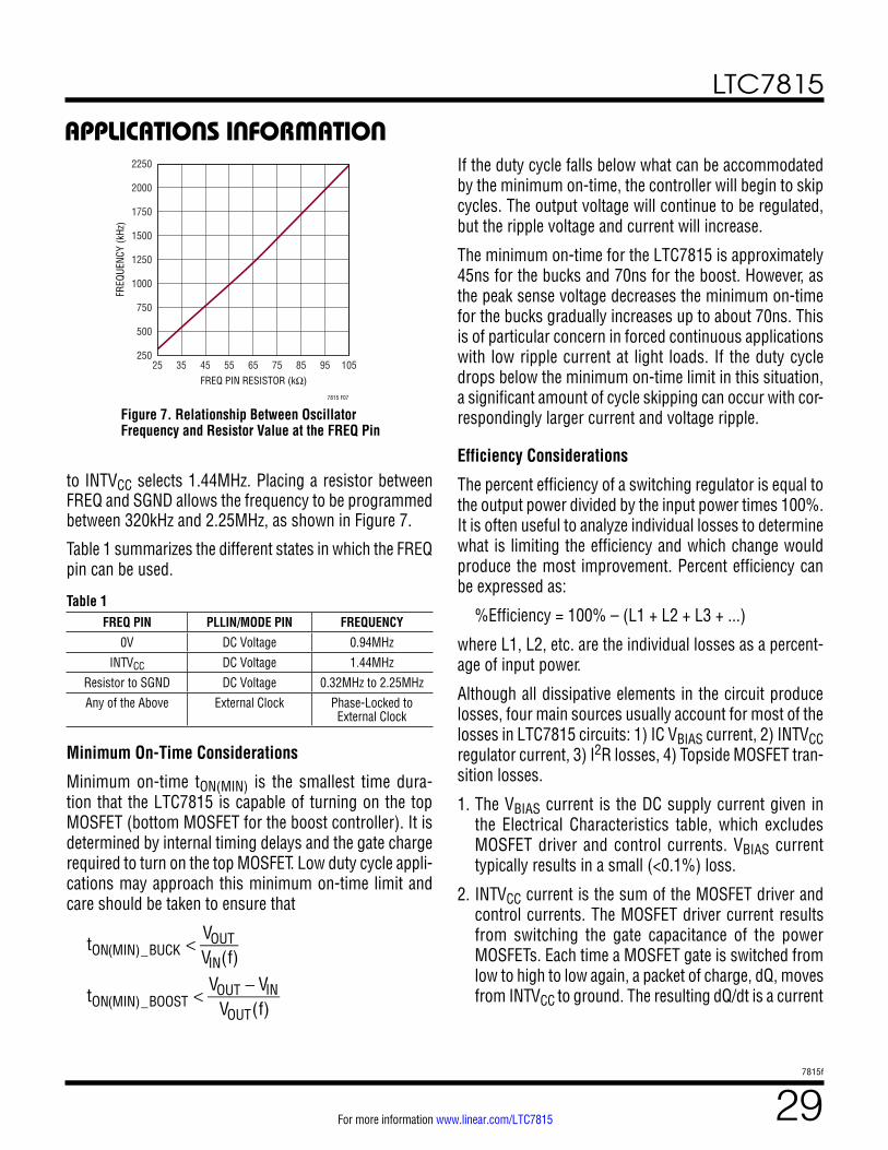
LTC7815
297815f
For more information www.linear.com/LTC7815
Figure 7. Relationship Between Oscillator Frequency and Resistor Value at the FREQ Pin
FREQ PIN RESISTOR (kΩ)
FREQ
UENC
Y (k
Hz)
7815 F07
25 35 45 55 65 75 85 95 105250
500
750
1000
1250
1500
1750
2000
2250
APPLICATIONS INFORMATION
to INTVCC selects 1.44MHz. Placing a resistor between FREQ and SGND allows the frequency to be programmed between 320kHz and 2.25MHz, as shown in Figure 7.
Table 1 summarizes the different states in which the FREQ pin can be used.
Table 1FREQ PIN PLLIN/MODE PIN FREQUENCY
0V DC Voltage 0.94MHzINTVCC DC Voltage 1.44MHz
Resistor to SGND DC Voltage 0.32MHz to 2.25MHzAny of the Above External Clock Phase-Locked to
External Clock
Minimum On-Time Considerations
Minimum on-time tON(MIN) is the smallest time dura-tion that the LTC7815 is capable of turning on the top MOSFET (bottom MOSFET for the boost controller). It is determined by internal timing delays and the gate charge required to turn on the top MOSFET. Low duty cycle appli-cations may approach this minimum on-time limit and care should be taken to ensure that
tON(MIN)_BUCK <VOUTVIN(f)
tON(MIN)_BOOST <VOUT − VIN
VOUT(f)
If the duty cycle falls below what can be accommodated by the minimum on-time, the controller will begin to skip cycles. The output voltage will continue to be regulated, but the ripple voltage and current will increase.
The minimum on-time for the LTC7815 is approximately 45ns for the bucks and 70ns for the boost. However, as the peak sense voltage decreases the minimum on-time for the bucks gradually increases up to about 70ns. This is of particular concern in forced continuous applications with low ripple current at light loads. If the duty cycle drops below the minimum on-time limit in this situation, a significant amount of cycle skipping can occur with cor-respondingly larger current and voltage ripple.
Efficiency Considerations
The percent efficiency of a switching regulator is equal to the output power divided by the input power times 100%. It is often useful to analyze individual losses to determine what is limiting the efficiency and which change would produce the most improvement. Percent efficiency can be expressed as:
%Efficiency = 100% – (L1 + L2 + L3 + ...)
where L1, L2, etc. are the individual losses as a percent-age of input power.
Although all dissipative elements in the circuit produce losses, four main sources usually account for most of the losses in LTC7815 circuits: 1) IC VBIAS current, 2) INTVCC regulator current, 3) I2R losses, 4) Topside MOSFET tran-sition losses.
1. The VBIAS current is the DC supply current given in the Electrical Characteristics table, which excludes MOSFET driver and control currents. VBIAS current typically results in a small (<0.1%) loss.
2. INTVCC current is the sum of the MOSFET driver and control currents. The MOSFET driver current results from switching the gate capacitance of the power MOSFETs. Each time a MOSFET gate is switched from low to high to low again, a packet of charge, dQ, moves from INTVCC to ground. The resulting dQ/dt is a current
LTC7815
307815f
For more information www.linear.com/LTC7815
APPLICATIONS INFORMATIONout of INTVCC that is typically much larger than the control circuit current. In continuous mode, IGATECHG = f(QT + QB), where QT and QB are the gate charges of the topside and bottom side MOSFETs.
Supplying INTVCC from an output-derived source power through EXTVCC will scale the VIN current required for the driver and control circuits by a fac-tor of (Duty Cycle)/(Efficiency). For example, in a 20V to 5V application, 10mA of INTVCC current results in approximately 2.5mA of VIN current. This reduces the mid-current loss from 10% or more (if the driver was powered directly from VIN) to only a few percent.
3. I2R losses are predicted from the DC resistances of the fuse (if used), MOSFET, inductor, current sense resis-tor, and input and output capacitor ESR. In continu-ous mode the average output current flows through L and RSENSE, but is “chopped” between the topside MOSFET and the synchronous MOSFET. If the two MOSFETs have approximately the same RDS(ON), then the resistance of one MOSFET can simply be summed with the resistances of L, RSENSE and ESR to obtain I2R losses. For example, if each RDS(ON) = 30mΩ, RL = 50mΩ, RSENSE = 10mΩ and RESR = 40mΩ (sum of both input and output capacitance losses), then the total resistance is 130mΩ. This results in losses rang-ing from 3% to 13% as the output current increases from 1A to 5A for a 5V output, or a 4% to 20% loss for a 3.3V output. Efficiency varies as the inverse square of VOUT for the same external components and output power level. The combined effects of increasingly lower output voltages and higher currents required by high performance digital systems is not doubling but qua-drupling the importance of loss terms in the switching regulator system!
4. Transition losses apply only to the top MOSFET(s) (bot-tom MOSFET for the boost), and become significant only when operating at high input voltages (typically 15V or greater). Transition losses can be estimated from:
Transition Loss = (1.7)VIN2 • IO(MAX) • CRSS • f
Other hidden losses such as copper trace and internal battery resistances can account for an additional 5% to 10% efficiency degradation in portable systems. It is very important to include these “system” level losses during the design phase. The internal battery and fuse resistance losses can be minimized by mak-ing sure that CIN has adequate charge storage and very low ESR at the switching frequency. A 25W supply will typically require a minimum of 20µF to 40µF of capacitance having a maximum of 20mΩ to 50mΩ of ESR. The LTC7815 2-phase architecture typically halves this input capacitance requirement over compet-ing solutions. Other losses including Schottky conduc-tion losses during dead-time and inductor core losses generally account for less than 2% total additional loss.
Checking Transient Response
The regulator loop response can be checked by looking at the load current transient response. Switching regulators take several cycles to respond to a step in DC (resistive) load current. When a load step occurs, VOUT shifts by an amount equal to ∆ILOAD • (ESR), where ESR is the effective series resistance of COUT. ∆ILOAD also begins to charge or discharge COUT generating the feedback error signal that forces the regulator to adapt to the current change and return VOUT to its steady-state value. During this recovery time VOUT can be monitored for excessive overshoot or ringing, which would indicate a stability problem. OPTI-LOOP compensation allows the transient response to be optimized over a wide range of output capacitance and ESR values. The availability of the ITH pin not only allows optimization of control loop behavior, but it also provides a DC coupled and AC filtered closed loop response test point. The DC step, rise time and settling at this test point truly reflects the closed loop response. Assuming a predominantly second order system, phase margin and/or damping factor can be estimated using the percentage of overshoot seen at this pin. The bandwidth can also be estimated by examining the rise time at the pin. The ITH external components shown in Figure 9 will provide an adequate starting point for most applications.
The ITH series RC-CC filter sets the dominant pole-zero loop compensation. The values can be modified slightly (from 0.5 to 2 times their suggested values) to optimize
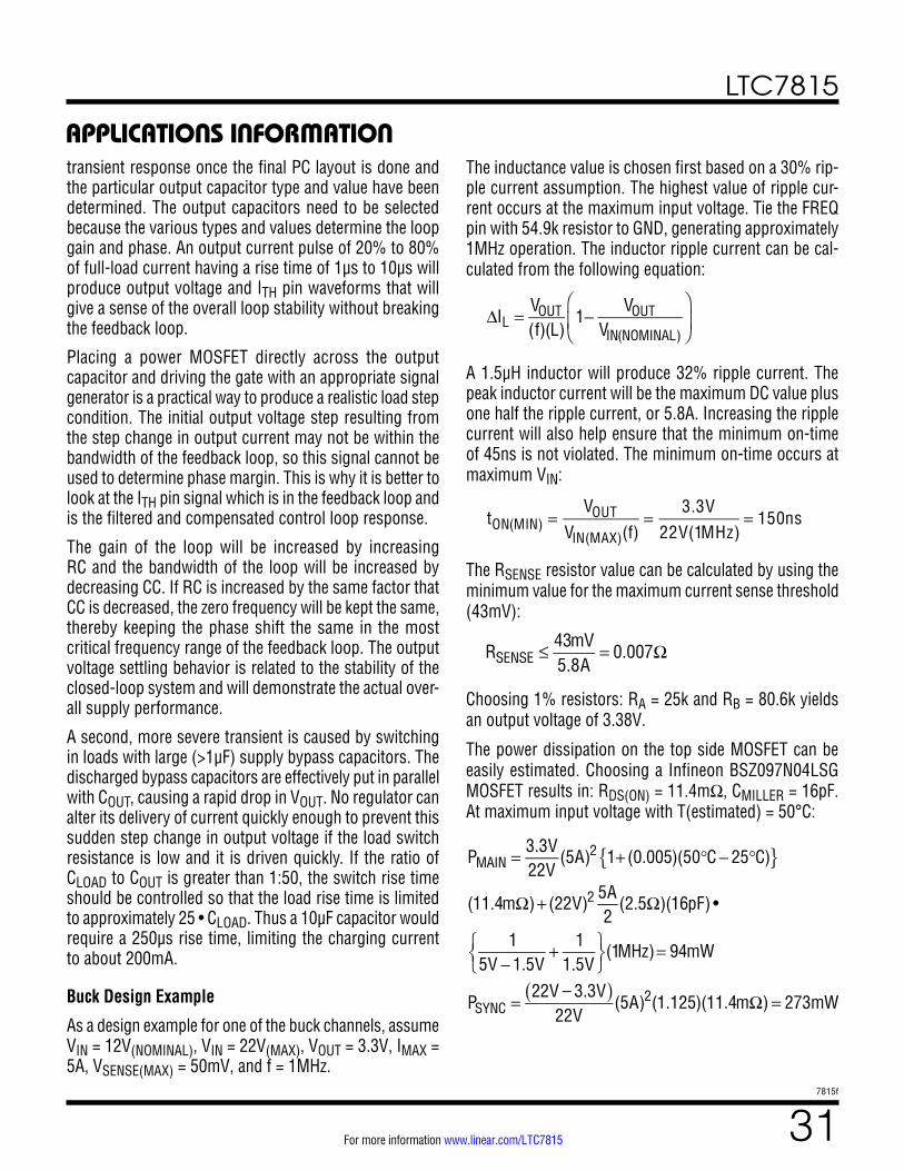
LTC7815
317815f
For more information www.linear.com/LTC7815
APPLICATIONS INFORMATIONtransient response once the final PC layout is done and the particular output capacitor type and value have been determined. The output capacitors need to be selected because the various types and values determine the loop gain and phase. An output current pulse of 20% to 80% of full-load current having a rise time of 1µs to 10µs will produce output voltage and ITH pin waveforms that will give a sense of the overall loop stability without breaking the feedback loop.
Placing a power MOSFET directly across the output capacitor and driving the gate with an appropriate signal generator is a practical way to produce a realistic load step condition. The initial output voltage step resulting from the step change in output current may not be within the bandwidth of the feedback loop, so this signal cannot be used to determine phase margin. This is why it is better to look at the ITH pin signal which is in the feedback loop and is the filtered and compensated control loop response.
The gain of the loop will be increased by increasing RC and the bandwidth of the loop will be increased by decreasing CC. If RC is increased by the same factor that CC is decreased, the zero frequency will be kept the same, thereby keeping the phase shift the same in the most critical frequency range of the feedback loop. The output voltage settling behavior is related to the stability of the closed-loop system and will demonstrate the actual over-all supply performance.
A second, more severe transient is caused by switching in loads with large (>1µF) supply bypass capacitors. The discharged bypass capacitors are effectively put in parallel with COUT, causing a rapid drop in VOUT. No regulator can alter its delivery of current quickly enough to prevent this sudden step change in output voltage if the load switch resistance is low and it is driven quickly. If the ratio of CLOAD to COUT is greater than 1:50, the switch rise time should be controlled so that the load rise time is limited to approximately 25 • CLOAD. Thus a 10µF capacitor would require a 250µs rise time, limiting the charging current to about 200mA.
Buck Design Example
As a design example for one of the buck channels, assume VIN = 12V(NOMINAL), VIN = 22V(MAX), VOUT = 3.3V, IMAX = 5A, VSENSE(MAX) = 50mV, and f = 1MHz.
The inductance value is chosen first based on a 30% rip-ple current assumption. The highest value of ripple cur-rent occurs at the maximum input voltage. Tie the FREQ pin with 54.9k resistor to GND, generating approximately 1MHz operation. The inductor ripple current can be cal-culated from the following equation:
ΔIL =
VOUT(f)(L)
1−VOUT
VIN(NOMINAL)
⎛
⎝⎜
⎞
⎠⎟
A 1.5µH inductor will produce 32% ripple current. The peak inductor current will be the maximum DC value plus one half the ripple current, or 5.8A. Increasing the ripple current will also help ensure that the minimum on-time of 45ns is not violated. The minimum on-time occurs at maximum VIN:
tON(MIN) =
VOUTVIN(MAX)(f)
=3.3V
22V(1MHz)= 150ns
The RSENSE resistor value can be calculated by using the minimum value for the maximum current sense threshold (43mV):
RSENSE ≤ 43mV
5.8A= 0.007Ω
Choosing 1% resistors: RA = 25k and RB = 80.6k yields an output voltage of 3.38V.
The power dissipation on the top side MOSFET can be easily estimated. Choosing a Infineon BSZ097N04LSG MOSFET results in: RDS(ON) = 11.4mΩ, CMILLER = 16pF. At maximum input voltage with T(estimated) = 50°C:
PMAIN = 3.3V22V
(5A)2 1+ (0.005)(50°C− 25°C)
(11.4mΩ)+ (22V)25A2
(2.5Ω)(16pF) •
15V −1.5V
+ 11.5V
⎧⎨⎩
⎫⎬⎭
(1MHz)= 94mW
PSYNC =22V – 3.3V( )
22V(5A)2(1.125)(11.4mΩ)= 273mW
LTC7815
327815f
For more information www.linear.com/LTC7815
APPLICATIONS INFORMATIONA short-circuit to ground will result in a folded back cur-rent of:
ISC = 20mV
0.007Ω− 1
240ns(22V)
1.5µH⎧⎨⎩
⎫⎬⎭= 2.56A
with a typical value of RDS(ON) and z = (0.005/°C)(25°C) = 0.125. The resulting power dissipated in the bottom MOSFET is:
PSYNC,SC = (2.56A)2(1.125)(11.4mΩ)= 84mW
The input capacitor to the buck regulator CIN is chosen for an RMS current rating of at least 3A at temperature. COUT is chosen with an ESR of 0.02Ω for low output ripple. The output ripple in continuous mode will be highest at the maximum input voltage. The output voltage ripple due to ESR is approximately:
VORIPPLE = RESR (∆IL) = 0.02Ω(1.6A) = 32mVP-P
PC Board Layout Checklist
When laying out the printed circuit board, the following checklist should be used to ensure proper operation of the IC. Figure 8 illustrates the current waveforms present in the various branches of the 2-phase synchronous buck regulators operating in the continuous mode. Check the following in your layout:
1. Are the top N-channel MOSFETs MTOP1 and MTOP2 located within 1cm of each other with a common drain connection at CIN? Do not attempt to split the input decoupling for the two channels as it can cause a large resonant loop.
2. Are the signal and power grounds kept separate? The combined IC signal ground pin and the ground return of CINTVCC must return to the combined COUT (–) ter-minals. The path formed by the top N-channel MOSFET, Schottky diode and the CIN capacitor should have short leads and PC trace lengths. The output capacitor (–) terminals should be connected as close as possible to the (–) terminals of the input capacitor by placing the capacitors next to each other and away from the Schottky loop described above.
3. Do the LTC7815 VFB pins’ resistive dividers connect to the (+) terminals of COUT? The resistive divider must be connected between the (+) terminal of COUT and signal ground. The feedback resistor connections should not be along the high current input feeds from the input capacitor(s).
4. Are the SENSE– and SENSE+ leads routed together with minimum PC trace spacing? The filter capacitor between SENSE+ and SENSE– should be as close as possible to the IC. Ensure accurate current sensing with Kelvin connections at the sense resistor.
5. Is the INTVCC decoupling capacitor connected close to the IC, between the INTVCC and the power ground pins? This capacitor carries the MOSFET drivers’ cur-rent peaks. An additional 1µF ceramic capacitor placed immediately next to the INTVCC and PGND pins can help improve noise performance substantially.
6. Keep the switching nodes (SW1, SW2, SW3), top gate nodes (TG1, TG2, TG3), and boost nodes (BOOST1, BOOST2, BOOST3) away from sensitive small-signal nodes, especially from the opposites channel’s voltage and current sensing feedback pins. All of these nodes have very large and fast moving signals and therefore should be kept on the output side of the LTC7815 and occupy minimum PC trace area.
7. Use a modified star ground technique: a low imped-ance, large copper area central grounding point on the same side of the PC board as the input and output capacitors with tie-ins for the bottom of the INTVCC decoupling capacitor, the bottom of the voltage feed-back resistive divider and the SGND pin of the IC.
PC Board Layout Debugging
Start with one controller on at a time. It is helpful to use a DC-50MHz current probe to monitor the current in the inductor while testing the circuit. Monitor the out-put switching node (SW pin) to synchronize the oscillo-scope to the internal oscillator and probe the actual out-put voltage as well. Check for proper performance over the operating voltage and current range expected in the
LTC7815
337815f
For more information www.linear.com/LTC7815
application. The frequency of operation should be main-tained over the input voltage range down to dropout and until the output load drops below the low current opera-tion threshold—typically 25% of the maximum designed current level in Burst Mode operation.
The duty cycle percentage should be maintained from cycle to cycle in a well-designed, low noise PCB imple-mentation. Variation in the duty cycle at a subharmonic rate can suggest noise pickup at the current or volt-age sensing inputs or inadequate loop compensation. Overcompensation of the loop can be used to tame a poor PC layout if regulator bandwidth optimization is not required. Only after each controller is checked for its indi-vidual performance should both controllers be turned on at the same time. A particularly difficult region of opera-tion is when one controller channel is nearing its current comparator trip point when the other channel is turning on its top MOSFET. This occurs around 50% duty cycle on either channel due to the phasing of the internal clocks and may cause minor duty cycle jitter.
Reduce VIN from its nominal level to verify operation of the regulator in dropout. Check the operation of the undervoltage lockout circuit by further lowering VIN while monitoring the outputs to verify operation.
APPLICATIONS INFORMATIONInvestigate whether any problems exist only at higher out-put currents or only at higher input voltages. If problems coincide with high input voltages and low output currents, look for capacitive coupling between the BOOST, SW, TG, and possibly BG connections and the sensitive voltage and current pins. The capacitor placed across the current sensing pins needs to be placed immediately adjacent to the pins of the IC. This capacitor helps to minimize the effects of differential noise injection due to high frequency capacitive coupling. If problems are encountered with high current output loading at lower input voltages, look for inductive coupling between CIN, Schottky and the top MOSFET components to the sensitive current and voltage sensing traces. In addition, investigate common ground path voltage pickup between these components and the SGND pin of the IC.
An embarrassing problem, which can be missed in an otherwise properly working switching regulator, results when the current sensing leads are hooked up backwards. The output voltage under this improper hookup will still be maintained but the advantages of current mode control will not be realized. Compensation of the voltage loop will be much more sensitive to component selection. This behavior can be investigated by temporarily shorting out the current sensing resistor—don’t worry, the regulator will still maintain control of the output voltage.
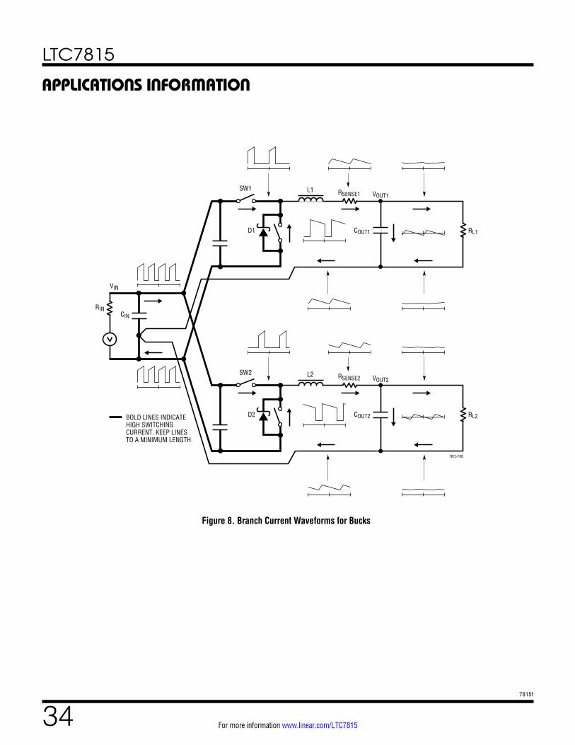
LTC7815
347815f
For more information www.linear.com/LTC7815
Figure 8. Branch Current Waveforms for Bucks
RL1D1
L1SW1 RSENSE1 VOUT1
COUT1
VIN
CINRIN
RL2D2BOLD LINES INDICATEHIGH SWITCHING CURRENT. KEEP LINESTO A MINIMUM LENGTH.
L2SW2
7815 F08
RSENSE2 VOUT2
COUT2
APPLICATIONS INFORMATION
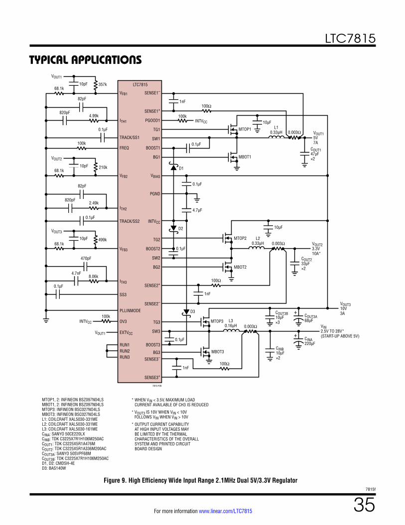
LTC7815
357815f
For more information www.linear.com/LTC7815
TYPICAL APPLICATIONS
Figure 9. High Efficiency Wide Input Range 2.1MHz Dual 5V/3.3V Regulator
7815 F09
LTC7815
SENSE1–
SENSE1+
PGOOD1
TG1
SW1
BOOST1
BG1
VBIAS
PGND
INTVCC
TG2
BOOST2
SW2
BG2
SENSE2+
SENSE2–
TG3
SW3
BOOST3
BG3
SENSE3–
SENSE3+
VFB1
ITH1
TRACK/SS1
FREQ
VFB2
ITH2
TRACK/SS2
VFB3
ITH3
SS3
1nF
100kINTVCC
100Ω
0.1µF
D1
D2
0.1µF
4.7µF
1nF
MTOP1
MBOT1
10µFL1
0.33µH 0.003Ω
COUT147µF×2
VOUT15V7A
MTOP2
MBOT2
L20.33µH 0.003Ω
COUT233µF×2
VOUT23.3V10A*
0.1µF
MTOP3
MBOT3
L30.16µH 0.003Ω
100Ω
1nF
D3PLLINMODE
0.1µF
CINB10µF×2
VIN2.5V TO 28V*(START-UP ABOVE 5V)
* WHEN VIN < 3.5V, MAXIMUM LOAD CURRENT AVAILABLE OF CH3 IS REDUCED
* VOUT3 IS 10V WHEN VIN < 10V FOLLOWS VIN WHEN VIN > 10V
* OUTPUT CURRENT CAPABILITY AT HIGH INPUT VOLTAGES MAY BE LIMITED BY THE THERMAL CHARACTERISTICS OF THE OVERALL SYSTEM AND PRINTED CIRCUIT BOARD DESIGN
COUT3B10µF×3
COUT3A68µF
357k10pF
VOUT1
68.1k
210k10pF
VOUT2
68.1k
82pF
820pF4.99k
82pF
820pF
0.1µF
2.49k
100Ω
499k10pF
VOUT3
68.1k
470pF
4.7nF
0.1µF
8.06k
0.1µF
MTOP1, 2: INFINEON BSZ097N04LSMBOT1, 2: INFINEON BSZ097N04LSMTOP3: INFINEON BSC027NO4LSMBOT3: INFINEON BSC027NO4LSL1: COILCRAFT XAL5030-331MEL2: COILCRAFT XAL5030-331MEL3: COILCRAFT XAL5030-161MECINA: SANYO 50CE220LXCINB: TDK C3225X7R1H106M250ACCOUT1: TDK C3225X5R1A476MCOUT2: TDK C3225X5R1A336M200ACCOUT3A: SANYO 50SVPF68MCOUT3B: TDK C3225X7R1H106M250ACD1, D2: CMDSH-4ED3: BAS140W
VOUT310V3A
OV3
+
CINA220µF
+
100k
10µF
100kINTVCC
EXTVCC
RUN1RUN2RUN3
VOUT1
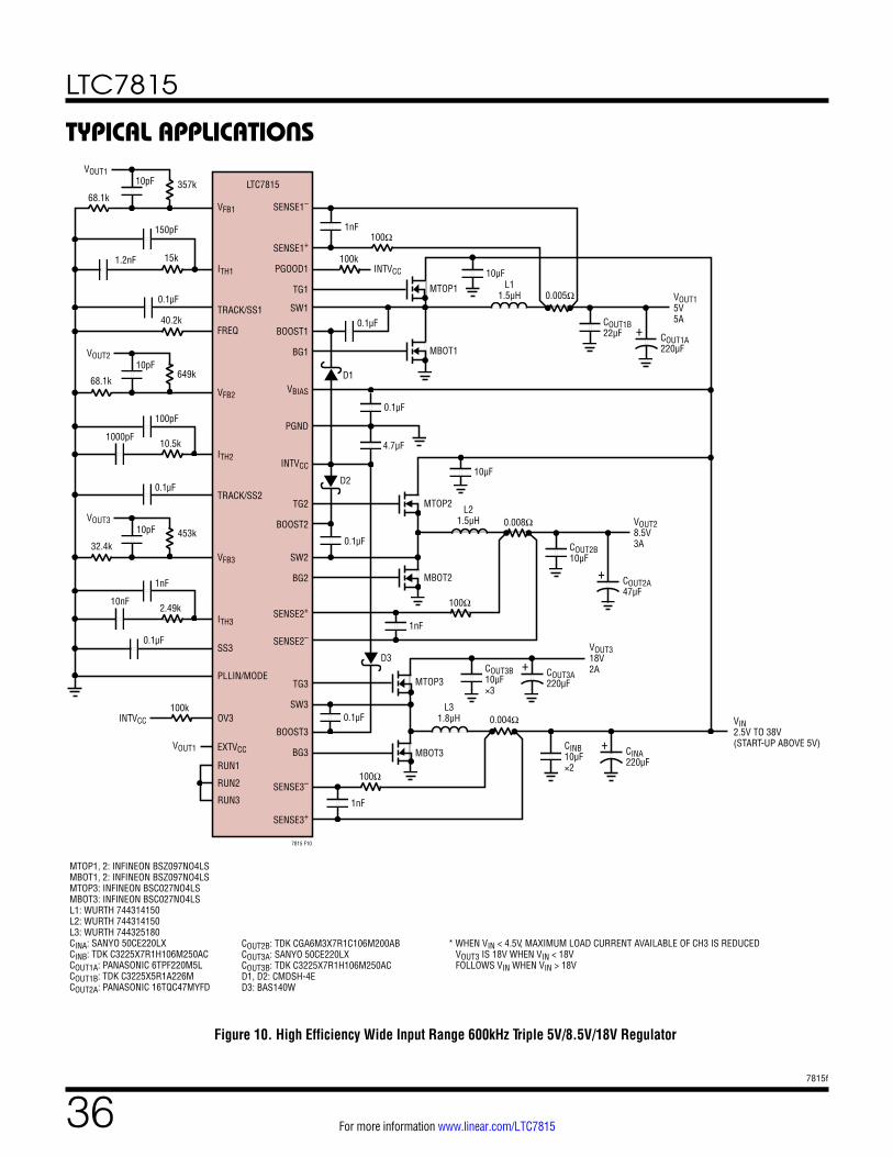
LTC7815
367815f
For more information www.linear.com/LTC7815
TYPICAL APPLICATIONS
7815 F10
LTC7815
SENSE1–
SENSE1+
PGOOD1
TG1
SW1
BOOST1
BG1
VBIAS
PGND
INTVCC
TG2
BOOST2
SW2
BG2
SENSE2+
SENSE2–
TG3
SW3
BOOST3
BG3
SENSE3–
SENSE3+
VFB1
ITH1
TRACK/SS1
FREQ
VFB2
ITH2
TRACK/SS2
VFB3
ITH3
SS3
1nF100Ω
0.1µF
D1
D2
0.1µF
4.7µF
0.1µF
1nF
0.1µF
MTOP1
MBOT1
10µFL1
1.5µH 0.005Ω
COUT1B22µF COUT1A
220µF
VOUT15V5A
MTOP2
MBOT2
10µF
L21.5µH 0.008Ω VOUT2
8.5V3A
VOUT318V2A
MTOP3
MBOT3
0.004Ω
1nF
* WHEN VIN < 4.5V, MAXIMUM LOAD CURRENT AVAILABLE OF CH3 IS REDUCED VOUT3 IS 18V WHEN VIN < 18V FOLLOWS VIN WHEN VIN > 18V
357k10pFVOUT1
68.1k
649k10pF
VOUT2
68.1k
150pF
1.2nF 15k
40.2k
100pF
0.1µF
1000pF10.5k
1nF
10nF2.49k
100k
453k10pFVOUT3
32.4k
0.1µF
0.1µF
MTOP1, 2: INFINEON BSZ097NO4LSMBOT1, 2: INFINEON BSZ097NO4LSMTOP3: INFINEON BSC027NO4LSMBOT3: INFINEON BSC027NO4LSL1: WURTH 744314150L2: WURTH 744314150L3: WURTH 744325180CINA: SANYO 50CE220LXCINB: TDK C3225X7R1H106M250ACCOUT1A: PANASONIC 6TPF220M5LCOUT1B: TDK C3225X5R1A226MCOUT2A: PANASONIC 16TQC47MYFD
COUT2B: TDK CGA6M3X7R1C106M200ABCOUT3A: SANYO 50CE220LXCOUT3B: TDK C3225X7R1H106M250ACD1, D2: CMDSH-4ED3: BAS140W
OV3INTVCC
PLLIN/MODE
RUN1
RUN2
RUN3
EXTVCCVOUT1
100kINTVCC
+
COUT2B10µF
COUT2A47µF
+
100Ω
L31.8µH
CINB10µF×2
CINA220µF
+
COUT3B10µF×3
VIN2.5V TO 38V(START-UP ABOVE 5V)
COUT3A220µF
+
100Ω
D3
Figure 10. High Efficiency Wide Input Range 600kHz Triple 5V/8.5V/18V Regulator
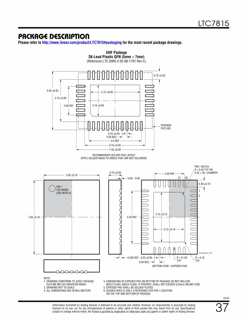
LTC7815
377815f
For more information www.linear.com/LTC7815
Information furnished by Analog Devices is believed to be accurate and reliable. However, no responsibility is assumed by Analog Devices for its use, nor for any infringements of patents or other rights of third parties that may result from its use. Specifications subject to change without notice. No license is granted by implication or otherwise under any patent or patent rights of Analog Devices.
5.00 ±0.10
NOTE:1. DRAWING CONFORMS TO JEDEC PACKAGE OUTLINE M0-220 VARIATION WHKD2. DRAWING NOT TO SCALE3. ALL DIMENSIONS ARE IN MILLIMETERS
PIN 1TOP MARK(SEE NOTE 6)
37
1
2
38
BOTTOM VIEW—EXPOSED PAD
5.50 REF5.15 ±0.10
7.00 ±0.10
0.75 ±0.05
R = 0.125TYP
R = 0.10TYP
0.25 ±0.05
(UH) QFN REF C 1107
0.50 BSC
0.200 REF
0.00 – 0.05
RECOMMENDED SOLDER PAD LAYOUTAPPLY SOLDER MASK TO AREAS THAT ARE NOT SOLDERED
3.00 REF
3.15 ±0.10
0.40 ±0.10
0.70 ±0.05
0.50 BSC5.5 REF
3.00 REF 3.15 ±0.05
4.10 ±0.05
5.50 ±0.05 5.15 ±0.05
6.10 ±0.05
7.50 ±0.05
0.25 ±0.05
PACKAGEOUTLINE
4. DIMENSIONS OF EXPOSED PAD ON BOTTOM OF PACKAGE DO NOT INCLUDE MOLD FLASH. MOLD FLASH, IF PRESENT, SHALL NOT EXCEED 0.20mm ON ANY SIDE5. EXPOSED PAD SHALL BE SOLDER PLATED6. SHADED AREA IS ONLY A REFERENCE FOR PIN 1 LOCATION ON THE TOP AND BOTTOM OF PACKAGE
PIN 1 NOTCHR = 0.30 TYP OR0.35 × 45° CHAMFER
UHF Package38-Lead Plastic QFN (5mm × 7mm)
(Reference LTC DWG # 05-08-1701 Rev C)
PACKAGE DESCRIPTIONPlease refer to http://www.linear.com/product/LTC7815#packaging for the most recent package drawings.
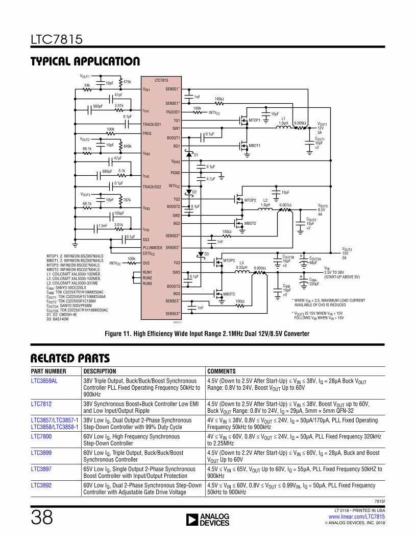
LTC7815
387815f
ANALOG DEVICES, INC. 2018
LT 0118 • PRINTED IN USAwww.linear.com/LTC7815
RELATED PARTS
TYPICAL APPLICATION
Figure 11. High Efficiency Wide Input Range 2.1MHz Dual 12V/8.5V Converter
PART NUMBER DESCRIPTION COMMENTSLTC3859AL 38V Triple Output, Buck/Buck/Boost Synchronous
Controller PLL Fixed Operating Frequency 50kHz to 900kHz
4.5V (Down to 2.5V After Start-Up) ≤ VIN ≤ 38V, IQ = 28μA Buck VOUT Range: 0.8V to 24V, Boost VOUT Up to 60V
LTC7812 38V Synchronous Boost+Buck Controller Low EMI and Low Input/Output Ripple
4.5V (Down to 2.5V After Start-Up) ≤ VIN ≤ 38V, Boost VOUT up to 60V, Buck VOUT Range: 0.8V to 24V, IQ = 29μA, 5mm × 5mm QFN-32
LTC3857/LTC3857-1 LTC3858/LTC3858-1
38V Low IQ, Dual Output 2-Phase Synchronous Step-Down Controller with 99% Duty Cycle
4V ≤ VIN ≤ 38V, 0.8V ≤ VOUT ≤ 24V, IQ = 50μA/170μA, PLL Fixed Operating Frequency 50kHz to 900kHz
LTC7800 60V Low IQ, High Frequency Synchronous Step-Down Controller
4V ≤ VIN ≤ 60V, 0.8V ≤ VOUT ≤ 24V, IQ = 50μA, PLL Fixed Frequency 320kHz to 2.25MHz
LTC3899 60V Low IQ, Triple Output, Buck/Buck/Boost Synchronous Controller
4.5V (Down to 2.2V After Start-Up) ≤ VIN ≤ 60V, IQ = 28μA, Buck and Boost VOUT Up to 60V
LTC3897 65V Low IQ, Single Output 2-Phase Synchronous Boost Controller with Input/Output Protection
4.5V ≤ VIN ≤ 65V, VOUT Up to 60V, IQ = 55μA, PLL Fixed Frequency 50kHZ to 900kHz
LTC3892 60V Low IQ, Dual 2-Phase Synchronous Step-Down Controller with Adjustable Gate Drive Voltage
4.5V ≤ VIN ≤ 60V, 0.8V ≤ VOUT ≤ 0.99VIN, IQ = 50μA, PLL Fixed Frequency 50kHz to 900kHz
7815 F11
LTC7815
SENSE1–
SENSE1+
PGOOD1
TG1
SW1
BOOST1
BG1
VBIAS
PGND
INTVCC
TG2
BOOST2
SW2
BG2
SENSE2+
SENSE2–
TG3
SW3
BOOST3
BG3
SENSE3–
SENSE3+
VFB1
ITH1
TRACK/SS1
FREQ
VFB2
ITH2
TRACK/SS2
VFB3
ITH3
SS3
1nF
100kINTVCC
100Ω
0.1µF
D1
D2
0.1µF
4.7µF
1nF
MTOP1
MBOT1
10µFL1
1.0µH 0.009Ω
COUT110µF×2
VOUT112V3A
MTOP2
MBOT2
L21.0µH 0.007Ω
COUT210µF×2
VOUT28.5V4A
0.1µF
MTOP3
MBOT3
L30.33µH 0.003Ω
100Ω
1nF
D3
0.1µF
CINB10µF×2
VIN2.5V TO 38V(START-UP ABOVE 5V)
* WHEN VIN < 3.5, MAXIMUM LOAD CURRENT AVAILABLE OF CH3 IS REDUCED
* VOUT3 IS 15V WHEN VIN < 15V FOLLOWS VIN WHEN VIN > 15V
COUT3B10µF×3
COUT3A68µF
475k10pF
VOUT1
34k
649k10pF
VOUT2
68.1k
47pF
560pF 3.01k
47µF
680pF
0.1µF
5.1k
787k10pFVOUT3
68.1k
150pF
1.5nF
0.1µF
3.01k
100k
0.1µF
MTOP1, 2: INFINEON BSZ097N04LSMBOT1, 2: INFINEON BSZ097N04LSMTOP3: INFINEON BSC027N04LSMBOT3: INFINEON BSC027N04LSL1: COILCRAFT XAL5030-102MEBL2: COILCRAFT XAL5030-102MEBL3: COILCRAFT XAL5030-331MECINA: SANYO 50CE220LXCINB: TDK C3225X7R1H106M250ACCOUT1: TDK C3225X5R1E106M250AACOUT2: TDK C3225X5R1C106MCOUT3A: SANYO 50SVPF68MCOUT3B: TDK C3225X7R1H106M250ACD1, D2: CMDSH-4ED3: BAS140W
VOUT315V2A+
CINA220µF
+
100k
10µF
100Ω
RUN1RUN2RUN3
PLLINMODEEXTVCC
OV3INTVCC