lm12cl 80w operational amplifier - mitweb.mit.edu/rec/datasheets/lm12cl.pdf · lm12cl 80w...
TRANSCRIPT
LM12CL80W Operational AmplifierGeneral DescriptionThe LM12 is a power op amp capable of driving ±25V at±10A while operating from ±30V supplies. The monolithic ICcan deliver 80W of sine wave power into a 4Ω load with0.01% distortion. Power bandwidth is 60 kHz. Further, apeak dissipation capability of 800W allows it to handle reac-tive loads such as transducers, actuators or small motorswithout derating. Important features include:
• input protection
• controlled turn on
• thermal limiting
• overvoltage shutdown
• output-current limiting
• dynamic safe-area protection
The IC delivers ±10A output current at any output voltageyet is completely protected against overloads, includingshorts to the supplies. The dynamic safe-area protection isprovided by instantaneous peak-temperature limiting withinthe power transistor array.
The turn-on characteristics are controlled by keeping theoutput open-circuited until the total supply voltage reaches14V. The output is also opened as the case temperature ex-
ceeds 150˚C or as the supply voltage approaches theBVCEO of the output transistors. The IC withstands overvolt-ages to 80V.
This monolithic op amp is compensated for unity-gain feed-back, with a small-signal bandwidth of 700 kHz. Slew rate is9V/µs, even as a follower. Distortion and capacitive-load sta-bility rival that of the best designs using complementary out-put transistors. Further, the IC withstands large differentialinput voltages and is well behaved should thecommon-mode range be exceeded.
The LM12 establishes that monolithic ICs can deliver consid-erable output power without resorting to complex switchingschemes. Devices can be paralleled or bridged for evengreater output capability. Applications include operationalpower supplies, high-voltage regulators, high-quality audioamplifiers, tape-head positioners, x-y plotters or otherservo-control systems.
The LM12 is supplied in a four-lead, TO-3 package with V−on the case. A gold-eutectic die-attach to a molybdenum in-terface is used to avoid thermal fatigue problems. The LM12is specified for either military or commercial temperaturerange.
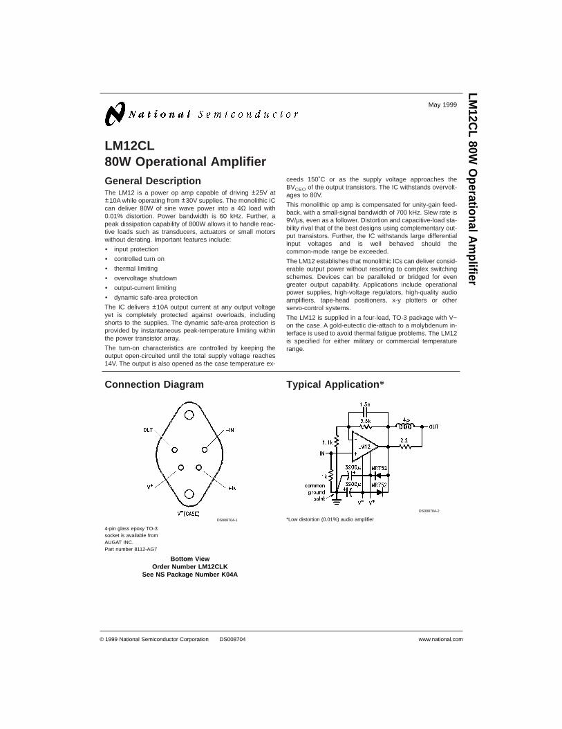
Connection Diagram Typical Application *
DS008704-1
4-pin glass epoxy TO-3socket is available fromAUGAT INC.Part number 8112-AG7
Bottom ViewOrder Number LM12CLK
See NS Package Number K04A
DS008704-2
*Low distortion (0.01%) audio amplifier
May 1999
LM12C
L80W
OperationalA
mplifier
© 1999 National Semiconductor Corporation DS008704 www.national.com

Absolute Maximum Ratings (Note 1)
If Military/Aerospace specified devices are required,please contact the National Semiconductor Sales Office/Distributors for availability and specifications.
Total Supply Voltage (Note 1) 80VInput Voltage (Note 2)Output Current Internally LimitedJunction Temperature (Note 3)
Storage Temperature Range −65˚C to 150˚CLead Temperature
(Soldering, 10 seconds) 300˚C
Operating RatingsTotal Supply Voltage 15V to 60VCase Temperature (Note 4) 0˚C to 70˚C
Electrical Characteristics (Note 4)
Parameter Conditions Typ25˚C
LM12CL Units
Limits
Input Offset Voltage ±10V ≤ VS ≤ ±0.5 VMAX, VCM = 0 2 15/20 mV (max)
Input Bias Current V− + 4V ≤ VCM ≤ V+ −2V 0.15 0.7/1.0 µA (max)
Input Offset Current V− +4V ≤ VCM ≤ V+ −2V 0.03 0.2/0.3 µA (max)
Common Mode V− +4V ≤ VCM ≤ V+ −2V 86 70/65 dB (min)
Rejection
Power Supply V+ = 0.5 VMAX, 90 70/65 dB (min)
Rejection −6V ≥ V− ≥ −0.5 VMAX
V− = −0.5 VMAX, 110 75/70 dB (min)
6V ≤ V+ ≤ 0.5 VMAX
Output Saturation tON = 1 ms,
Threshold ∆VIN = 5 (10 ) mV,
IOUT = 1A 1.8 2.2/2.5 V (max)
8A 4 5/7 V (max)
10A 5 V (max)
Large Signal Voltage tON = 2 ms,
Gain VSAT = 2V, IOUT = 0 100 30/20 V/mV (min)
VSAT = 8V, RL = 4Ω 50 15/10 V/mV (min)
Thermal Gradient PDISS = 50W, tON = 65 ms 30 100 µV/W (max)
Feedback
Output-Current Limit tON = 10 ms, VDISS = 10V 13 16 A (max)
tON = 100 ms, VDISS = 58V 1.5 0.9/0.6 A (min)
1.5 1.7 A (max)
Power Dissipation tON = 100 ms, VDISS = 20V 100 80/55 W (min)
Rating VDISS = 58V 80 52/35 W (min)
DC Thermal Resistance (Note 5) VDISS = 20V 2.3 2.9 ˚C/W (max)
VDISS = 58V 2.7 4.5 ˚C/W (max)
AC Thermal Resistance (Note 5) 1.6 2.1 ˚C/W (max)
Supply Current VOUT = 0, IOUT = 0 60 120/140 mA (max)
Note 1: Absolute maximum ratings indicate limits beyond which damage to the device may occur. The maximum voltage for which the LM12 is guaranteed to operateis given in the operating ratings and in Note 4. With inductive loads or output shorts, other restrictions described in applications section apply.
Note 2: Neither input should exceed the supply voltage by more than 50 volts nor should the voltage between one input and any other terminal exceed 60 volts.
Note 3: Operating junction temperature is internally limited near 225˚C within the power transistor and 160˚C for the control circuitry.
Note 4: The supply voltage is ±30V (VMAX = 60V), unless otherwise specified. The voltage across the conducting output transistor (supply to output) is VDISS andinternal power dissipation is PDISS. Temperature range is 0˚C ≤ TC ≤ 70˚C where TC is the case temperature. Standard typeface indicates limits at 25˚C while bold-face type refers to limits or special conditions over full temperature range. With no heat sink, the package will heat at a rate of 35˚C/sec per 100W of internaldissipation.
Note 5: This thermal resistance is based upon a peak temperature of 200˚C in the center of the power transistor and a case temperature of 25˚C measured at thecenter of the package bottom. The maximum junction temperature of the control circuitry can be estimated based upon a dc thermal resistance of 0.9˚C/W or an acthermal resistance of 0.6˚C/W for any operating voltage.
Although the output and supply leads are resistant to electrostatic discharges from handling, the input leads are not.The part should be treated accordingly.
www.national.com 2
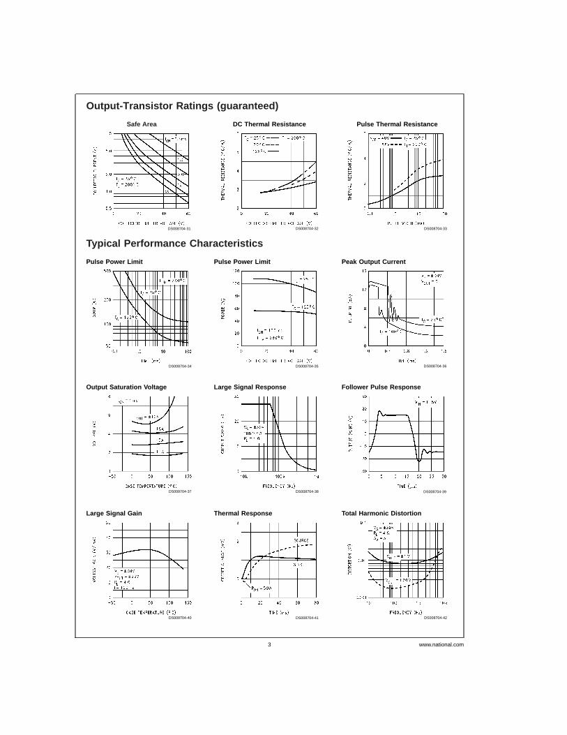
Output-Transistor Ratings (guaranteed)
Typical Performance Characteristics
Safe Area
DS008704-31
DC Thermal Resistance
DS008704-32
Pulse Thermal Resistance
DS008704-33
Pulse Power Limit
DS008704-34
Pulse Power Limit
DS008704-35
Peak Output Current
DS008704-36
Output Saturation Voltage
DS008704-37
Large Signal Response
DS008704-38
Follower Pulse Response
DS008704-39
Large Signal Gain
DS008704-40
Thermal Response
DS008704-41
Total Harmonic Distortion
DS008704-42
www.national.com3

Typical Performance Characteristics (Continued)
Application Information
GENERAL
Twenty five years ago the operational amplifier was a spe-cialized design tool used primarily for analog computation.However, the availability of low cost IC op amps in the late1960’s prompted their use in rather mundane applications,replacing a few discrete components. Once a few basic prin-ciples are mastered, op amps can be used to give exception-ally good results in a wide range of applications while mini-mizing both cost and design effort.
The availability of a monolithic power op amp now promisesto extend these advantages to high-power designs. Someconventional applications are given here to illustrate op ampdesign principles as they relate to power circuitry. The inevi-table fall in prices, as the economies of volume production
are realized, will prompt their use in applications that mightnow seem trivial. Replacing single power transistors with anop amp will become economical because of improved per-formance, simplification of attendant circuitry, vastly im-proved fault protection, greater reliability and the reduction ofdesign time.
Power op amps introduce new factors into the design equa-tion. With current transients above 10A, both the inductanceand resistance of wire interconnects become important in anumber of ways. Further, power ratings are a crucial factor indetermining performance. But the power capability of the ICcannot be realized unless it is properly mounted to an ad-equate heat sink. Thus, thermal design is of major impor-tance with power op amps.
This application summary starts off by identifying the originof strange problems observed while using the LM12 in a
Frequency Response
DS008704-43
Output Impedance
DS008704-44
Power Supply Rejection
DS008704-45
Input Bias Current
DS008704-46
Input Noise Voltage
DS008704-47
Common Mode Rejection
DS008704-48
Supply Current
DS008704-49
Supply Current
DS008704-50
Cross-Supply Current
DS008704-51
www.national.com 4
Application Information (Continued)
wide variety of designs with all sorts of fault conditions. A fewsimple precautions will eliminate these problems. Onewould do well to read the section on supply bypassing,lead inductance, output clamp diodes, ground loops andreactive loading before doing any experimentation.Should there be problems with erratic operation,blow-outs, excessive distortion or oscillation, anotherlook at these sections is in order.
The management and protection circuitry can also affect op-eration. Should the total supply voltage exceed ratings ordrop below 15–20V, the op amp shuts off completely. Casetemperatures above 150˚C also cause shut down until thetemperature drops to 145˚C. This may take several seconds,depending on the thermal system. Activation of the dynamicsafe-area protection causes both the main feedback loop tolose control and a reduction in output power, with possibleoscillations. In ac applications, the dynamic protection willcause waveform distortion. Since the LM12 is well protectedagainst thermal overloads, the suggestions for determiningpower dissipation and heat sink requirements are presentedlast.
SUPPLY BYPASSING
All op amps should have their supply leads bypassed withlow-inductance capacitors having short leads and locatedclose to the package terminals to avoid spurious oscillationproblems. Power op amps require larger bypass capacitors.The LM12 is stable with good-quality electrolytic bypass ca-pacitors greater than 20 µF. Other considerations may re-quire larger capacitors.
The current in the supply leads is a rectified component ofthe load current. If adequate bypassing is not provided, thisdistorted signal can be fed back into internal circuitry. Lowdistortion at high frequencies requires that the supplies bebypassed with 470 µF or more, at the package terminals.
LEAD INDUCTANCE
With ordinary op amps, lead-inductance problems are usu-ally restricted to supply bypassing. Power op amps are alsosensitive to inductance in the output lead, particularly withheavy capacitive loading. Feedback to the input should betaken directly from the output terminal, minimizing commoninductance with the load. Sensing to a remote load must beaccompanied by a high-frequency feedback path directlyfrom the output terminal. Lead inductance can also causevoltage surges on the supplies. With long leads to the powersource, energy stored in the lead inductance when the out-put is shorted can be dumped back into the supply bypasscapacitors when the short is removed. The magnitude of thistransient is reduced by increasing the size of the bypass ca-pacitor near the IC. With 20 µF local bypass, these voltagesurges are important only if the lead length exceeds a couplefeet (> 1 µH lead inductance). Twisting together the supplyand ground leads minimizes the effect.
GROUND LOOPS
With fast, high-current circuitry, all sorts of problems canarise from improper grounding. In general, difficulties can beavoided by returning all grounds separately to a commonpoint. Sometimes this is impractical. When compromising,special attention should be paid to the ground returns for thesupply bypasses, load and input signal. Ground planes alsohelp to provide proper grounding.
Many problems unrelated to system performance can betraced to the grounding of line-operated test equipment usedfor system checkout. Hidden paths are particularly difficult tosort out when several pieces of test equipment are used butcan be minimized by using current probes or the new iso-lated oscilloscope pre-amplifiers. Eliminating any directground connection between the signal generator and the os-cilloscope synchronization input solves one common prob-lem.
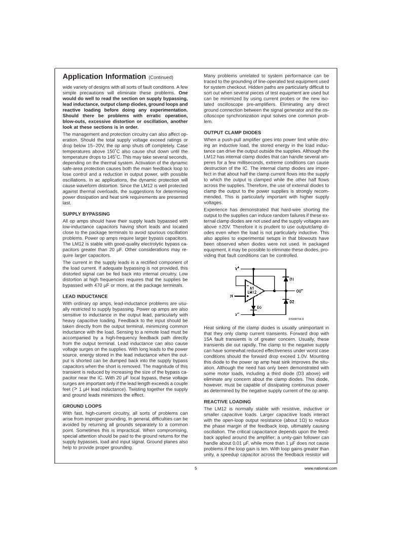
OUTPUT CLAMP DIODES
When a push-pull amplifier goes into power limit while driv-ing an inductive load, the stored energy in the load induc-tance can drive the output outside the supplies. Although theLM12 has internal clamp diodes that can handle several am-peres for a few milliseconds, extreme conditions can causedestruction of the IC. The internal clamp diodes are imper-fect in that about half the clamp current flows into the supplyto which the output is clamped while the other half flowsacross the supplies. Therefore, the use of external diodes toclamp the output to the power supplies is strongly recom-mended. This is particularly important with higher supplyvoltages.
Experience has demonstrated that hard-wire shorting theoutput to the supplies can induce random failures if these ex-ternal clamp diodes are not used and the supply voltages areabove ±20V. Therefore it is prudent to use outputclamp di-odes even when the load is not particularly inductive. Thisalso applies to experimental setups in that blowouts havebeen observed when diodes were not used. In packagedequipment, it may be possible to eliminate these diodes, pro-viding that fault conditions can be controlled.
Heat sinking of the clamp diodes is usually unimportant inthat they only clamp current transients. Forward drop with15A fault transients is of greater concern. Usually, thesetransients die out rapidly. The clamp to the negative supplycan have somewhat reduced effectiveness under worst caseconditions should the forward drop exceed 1.0V. Mountingthis diode to the power op amp heat sink improves the situ-ation. Although the need has only been demonstrated withsome motor loads, including a third diode (D3 above) willeliminate any concern about the clamp diodes. This diode,however, must be capable of dissipating continuous poweras determined by the negative supply current of the op amp.
REACTIVE LOADING
The LM12 is normally stable with resistive, inductive orsmaller capacitive loads. Larger capacitive loads interactwith the open-loop output resistance (about 1Ω) to reducethe phase margin of the feedback loop, ultimately causingoscillation. The critical capacitance depends upon the feed-back applied around the amplifier; a unity-gain follower canhandle about 0.01 µF, while more than 1 µF does not causeproblems if the loop gain is ten. With loop gains greater thanunity, a speedup capacitor across the feedback resistor will
DS008704-6
www.national.com5

Application Information (Continued)
aid stability. In all cases, the op amp will behave predictablyonly if the supplies are properly bypassed, ground loops arecontrolled and high-frequency feedback is derived directlyfrom the output terminal, as recommended earlier.
So-called capacitive loads are not always capacitive. Ahigh-Q capacitor in combination with long leads can presenta series-resonant load to the op amp. In practice, this is notusually a problem; but the situation should be kept in mind.
Large capacitive loads (including series-resonant) can beaccommodated by isolating the feedback amplifier from theload as shown above. The inductor gives low output imped-ance at lower frequencies while providing an isolating im-pedance at high frequencies. The resistor kills the Q of se-ries resonant circuits formed by capacitive loads. A lowinductance, carbon-composition resistor is recommended.Optimum values of L and R depend upon the feedback gainand expected nature of the load, but are not critical. A 4 µHinductor is obtained with 14 turns of number 18 wire, closespaced, around a one-inch-diameter form.
The LM12 can be made stable for all loads with a large ca-pacitor on the output, as shown above. This compensationgives the lowest possible closed-loop output impedance athigh frequencies and the best load-transient response. It isappropriate for such applications as voltage regulators.
A feedback capacitor, C1, is connected directly to the outputpin of the IC. The output capacitor, C2, is connected at theoutput terminal with short leads. Single-point grounding toavoid dc and ac ground loops is advised.
The impedance, Z1, is the wire connecting the op amp outputto the load capacitor. About 3-inches of number-18 wire(70 nH) gives good stability and 18-inches (400 nH) beginsto degrade load-transient response. The minimum load ca-pacitance is 47 µF, if a solid-tantalum capacitor with anequivalent series resistance (ESR) of 0.1Ω is used. Electro-lytic capacitors work as well, although capacitance may haveto be increased to 200 µF to bring ESR below 0.1Ω.
Loop stability is not the only concern when op amps are op-erated with reactive loads. With time-varying signals, powerdissipation can also increase markedly. This is particularlytrue with the combination of capacitive loads andhigh-frequency excitation.
INPUT COMPENSATION
The LM12 is prone to low-amplitude oscillation bursts com-ing out of saturation if the high-frequency loop gain is nearunity. The voltage follower connection is most susceptible.This glitching can be eliminated at the expense ofsmall-signal bandwidth using input compensation. Inputcompensation can also be used in combination with LR loadisolation to improve capacitive load stability.
An example of a voltage follower with input compensation isshown here. The R2C2 combination across the input workswith R1 to reduce feedback at high frequencies withoutgreatly affecting response below 100 kHz. A lead capacitor,C1, improves phase margin at the unity-gain crossover fre-quency. Proper operation requires that the output impedanceof the circuitry driving the follower be well under 1 kΩ at fre-quencies up to a few hundred kilohertz.
Extending input compensation to the integrator connection isshown here. Both the follower and this integrator will handle1 µF capacitive loading without LR output isolation.
CURRENT DRIVE
This circuit provides an output current proportional to the in-put voltage. Current drive is sometimes preferred for servomotors because it aids in stabilizing the servo loop by reduc-ing phase lag caused by motor inductance. In applicationsrequiring high output resistance, such as operational powersupplies running in the current mode, matching of the feed-back resistors to 0.01% is required. Alternately, an adjust-able resistor can be used for trimming.
DS008704-7
DS008704-8
DS008704-9
DS008704-10
DS008704-11
www.national.com 6
Application Information (Continued)
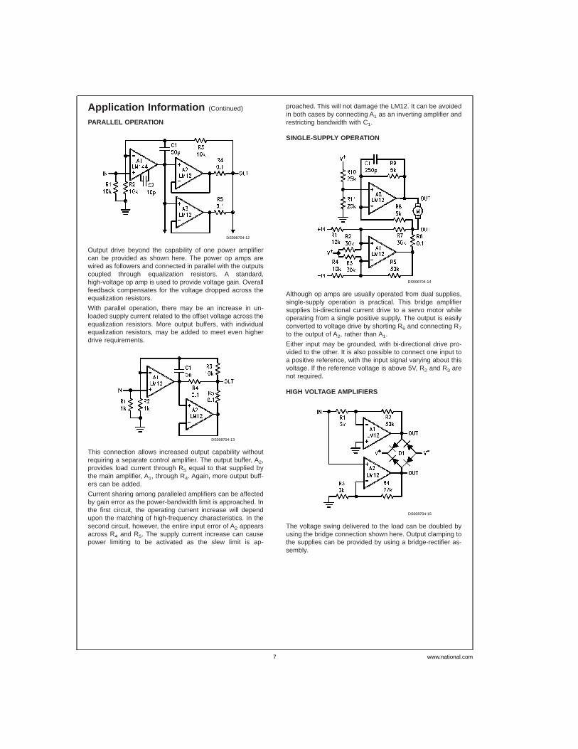
PARALLEL OPERATION
Output drive beyond the capability of one power amplifiercan be provided as shown here. The power op amps arewired as followers and connected in parallel with the outputscoupled through equalization resistors. A standard,high-voltage op amp is used to provide voltage gain. Overallfeedback compensates for the voltage dropped across theequalization resistors.
With parallel operation, there may be an increase in un-loaded supply current related to the offset voltage across theequalization resistors. More output buffers, with individualequalization resistors, may be added to meet even higherdrive requirements.
This connection allows increased output capability withoutrequiring a separate control amplifier. The output buffer, A2,provides load current through R5 equal to that supplied bythe main amplifier, A1, through R4. Again, more output buff-ers can be added.
Current sharing among paralleled amplifiers can be affectedby gain error as the power-bandwidth limit is approached. Inthe first circuit, the operating current increase will dependupon the matching of high-frequency characteristics. In thesecond circuit, however, the entire input error of A2 appearsacross R4 and R5. The supply current increase can causepower limiting to be activated as the slew limit is ap-
proached. This will not damage the LM12. It can be avoidedin both cases by connecting A1 as an inverting amplifier andrestricting bandwidth with C1.
SINGLE-SUPPLY OPERATION
Although op amps are usually operated from dual supplies,single-supply operation is practical. This bridge amplifiersupplies bi-directional current drive to a servo motor whileoperating from a single positive supply. The output is easilyconverted to voltage drive by shorting R6 and connecting R7
to the output of A2, rather than A1.
Either input may be grounded, with bi-directional drive pro-vided to the other. It is also possible to connect one input toa positive reference, with the input signal varying about thisvoltage. If the reference voltage is above 5V, R2 and R3 arenot required.
HIGH VOLTAGE AMPLIFIERS
The voltage swing delivered to the load can be doubled byusing the bridge connection shown here. Output clamping tothe supplies can be provided by using a bridge-rectifier as-sembly.
DS008704-12
DS008704-13
DS008704-14
DS008704-15
www.national.com7
Application Information (Continued)
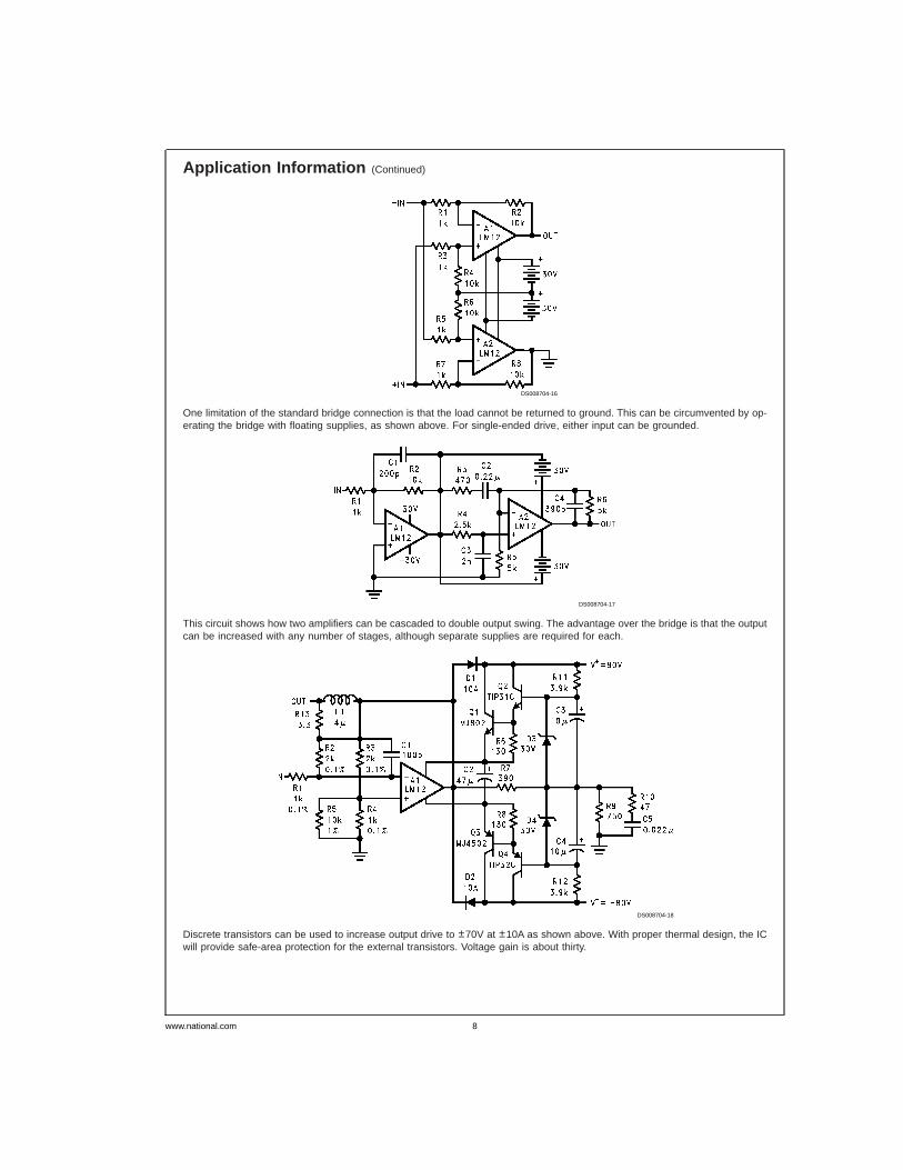
One limitation of the standard bridge connection is that the load cannot be returned to ground. This can be circumvented by op-erating the bridge with floating supplies, as shown above. For single-ended drive, either input can be grounded.
This circuit shows how two amplifiers can be cascaded to double output swing. The advantage over the bridge is that the outputcan be increased with any number of stages, although separate supplies are required for each.
Discrete transistors can be used to increase output drive to ±70V at ±10A as shown above. With proper thermal design, the ICwill provide safe-area protection for the external transistors. Voltage gain is about thirty.
DS008704-16
DS008704-17
DS008704-18
www.national.com 8
Application Information (Continued)
OPERATIONAL POWER SUPPLY
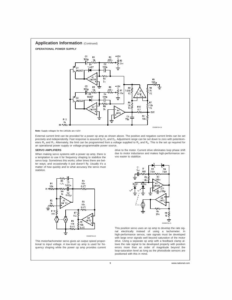
External current limit can be provided for a power op amp as shown above. The positive and negative current limits can be setprecisely and independently. Fast response is assured by D1 and D2. Adjustment range can be set down to zero with potentiom-eters R3 and R7. Alternately, the limit can be programmed from a voltage supplied to R2 and R6. This is the set up required foran operational power supply or voltage-programmable power source.
SERVO AMPLIFIERS
When making servo systems with a power op amp, there isa temptation to use it for frequency shaping to stabilize theservo loop. Sometimes this works; other times there are bet-ter ways; and occasionally it just doesn’t fly. Usually it’s amatter of how quickly and to what accuracy the servo muststabilize.
This motor/tachometer servo gives an output speed propor-tional to input voltage. A low-level op amp is used for fre-quency shaping while the power op amp provides current
drive to the motor. Current drive eliminates loop phase shiftdue to motor inductance and makes high-performance ser-vos easier to stabilize.
This position servo uses an op amp to develop the rate sig-nal electrically instead of using a tachometer. Inhigh-performance servos, rate signals must be developedwith large error signals well beyond saturation of the motordrive. Using a separate op amp with a feedback clamp al-lows the rate signal to be developed properly with positionerrors more than an order of magnitude beyond theloop-saturation level as long as the photodiode sensors arepositioned with this in mind.
DS008704-19
Note: Supply voltages for the LM318s are ±15V
DS008704-20
DS008704-21
www.national.com9

Application Information (Continued)
VOLTAGE REGULATORS
An op amp can be used as a positive or negative regulator.Unlike most regulators, it can sink current to absorb energydumped back into the output. This positive regulator has a0–50V output range.
Dual supplies are not required to use an op amp as a voltageregulator if zero output is not required. This 4V to 50V regu-lator operates from a single supply. Should the op amp notbe able to absorb enough energy to control an overvoltagecondition, a SCR will crowbar the output.
REMOTE SENSING
Remote sensing as shown above allows the op amp to cor-rect for dc drops in cables connecting the load. Even so,cable drop will affect transient response. Degradation can beminimized by using twisted, heavy-gauge wires on the out-put line. Normally, common and one input are connected to-gether at the sending end.
AUDIO AMPLIFIERS
A power amplifier suitable for use in high-quality audio equip-ment is shown above. Harmonic distortion is about0.01-percent. Intermodulation distortion (60 Hz/7 kHz, 4:1)measured 0.015-percent. Transient response and saturationrecovery are clean, and the 9 V/µs slew rate of the LM12 vir-tually eliminates transient intermodulation distortion. Usingseparate amplifiers to drive low- and high-frequency speak-ers gets rid of high-level crossover networks and attenua-tors. Further, it prevents clipping on the low-frequency chan-nel from distorting the high frequencies.
DETERMINING MAXIMUM DISSIPATION
It is a simple matter to establish power requirements for anop amp driving a resistive load at frequencies well below10 Hz. Maximum dissipation occurs when the output is atone-half the supply voltage with high-line conditions. The in-dividual output transistors must be rated to handle this powercontinuously at the maximum expected case temperature.The power rating is limited by the maximum junction tem-perature as determined by
TJ = TC + PDISS θJC,
where TC is the case temperature as measured at the centerof the package bottom, PDISS is the maximum power dissipa-tion and θJC is the thermal resistance at the operating volt-age of the output transistor. Recommended maximum junc-tion temperatures are 200˚C within the power transistor and150˚C for the control circuitry.
If there is ripple on the supply bus, it is valid to use the aver-age value in worst-case calculations as long as the peak rat-ing of the power transistor is not exceeded at the ripple peak.With 120 Hz ripple, this is 1.5 times the continuous powerrating.
Dissipation requirements are not so easily established withtime varying output signals, especially with reactive loads.Both peak and continuous dissipation ratings must be takeninto account, and these depend on the signal waveform aswell as load characteristics.
With a sine wave output, analysis is fairly straightforward.With supply voltages of ±VS, the maximum average powerdissipation of both output transistors is
DS008704-22
DS008704-23
DS008704-24
DS008704-25
www.national.com 10

Application Information (Continued)
where ZL is the magnitude of the load impedance and θ itsphase angle. Maximum average dissipation occurs belowmaximum output swing for θ < 40˚.
The instantaneous power dissipation over the conductinghalf cycle of one output transistor is shown here. Power dis-sipation is near zero on the other half cycle. The output levelis that resulting in maximum peak and average dissipation.Plots are given for a resistive and a series RL load. The latteris representative of a 4Ω loudspeaker operating below reso-nance and would be the worst case condition in most audioapplications. The peak dissipation of each transistor is aboutfour times average. In ac applications, power capability is of-ten limited by the peak ratings of the power transistor.
The pulse thermal resistance of the LM12 is specified forconstant power pulse duration. Establishing an exactequivalency between constant-power pulses and those en-countered in practice is not easy. However, for sine waves,reasonable estimates can be made at any frequency by as-suming a constant power pulse amplitude given by:
where φ = 60˚ and θ is the absolute value of the phase angleof ZL. Equivalent pulse width is tON ≅ 0.4τ for θ = 0 and tON
≅ 0.2τ for θ ≥ 20˚, where τ is the period of the output wave-form.
DISSIPATION DRIVING MOTORS
A motor with a locked rotor looks like an inductance in serieswith a resistance, for purposes of determining driver dissipa-tion. With slow-response servos, the maximum signal ampli-tude at frequencies where motor inductance is significantcan be so small that motor inductance does not have to betaken into account. If this is the case, the motor can betreated as a simple, resistive load as long as the rotor speedis low enough that the back emf is small by comparison tothe supply voltage of the driver transistor.
A permanent-magnet motor can build up a back emf that isequal to the output swing of the op amp driving it. Reversingthis motor from full speed requires the output drive transistorto operate, initially, along a loadline based upon the motorresistance and total supply voltage. Worst case, this loadlinewill have to be within the continuous dissipation rating of thedrive transistor; but system dynamics may permit taking ad-vantage of the higher pulse ratings. Motor inductance cancause added stress if system response is fast.
Shunt- and series-wound motors can generate back emf’sthat are considerably more than the total supply voltage, re-
sulting in even higher peak dissipation than apermanent-magnet motor having the same locked-rotor re-sistance.
VOLTAGE REGULATOR DISSIPATION
The pass transistor dissipation of a voltage regulator is eas-ily determined in the operating mode. Maximum continuousdissipation occurs with high line voltage and maximum loadcurrent. As discussed earlier, ripple voltage can be averagedif peak ratings are not exceeded; however, a higher averagevoltage will be required to insure that the pass transistordoes not saturate at the ripple minimum.
Conditions during start-up can be more complex. If the inputvoltage increases slowly such that the regulator does not gointo current limit charging output capacitance, there are noproblems. If not, load capacitance and load characteristicsmust be taken into account. This is also the case if automaticrestart is required in recovering from overloads.
Automatic restart or start-up with fast-rising input voltagescannot be guaranteed unless the continuous dissipation rat-ing of the pass transistor is adequate to supply the load cur-rent continuously at all voltages below the regulated outputvoltage. In this regard, the LM12 performs much better thanIC regulators using foldback current limit, especially withhigh-line input voltage above 20V.
POWER LIMITING
Should the power ratings of the LM12 be exceeded, dynamicsafe-area protection is activated. Waveforms with this powerlimiting are shown for the LM12 driving ±26V at 30 Hz into3Ω in series with 24 mH (θ = 45˚). With an inductive load, theoutput clamps to the supplies in power limit, as above. Withresistive loads, the output voltage drops in limit. Behaviorwith more complex RCL loads is between these extremes.
Secondary thermal limit is activated should the case tem-perature exceed 150˚C. This thermal limit shuts down the ICcompletely (open output) until the case temperature drops toabout 145˚C. Recovery may take several seconds.
POWER SUPPLIES
Power op amps do not require regulated supplies. However,the worst-case output power is determined by the low-linesupply voltage in the ripple trough. The worst-case powerdissipation is established by the average supply voltage withhigh-line conditions. The loss in power output that can beguaranteed is the square of the ratio of these two voltages.
Relatively simple off-line switching power supplies can pro-vide voltage conversion, line isolation and 5-percent regula-tion while reducing size and weight.
The regulation against ripple and line variations can providea substantial increase in the power output that can be guar-
DS008704-26
DS008704-27
www.national.com11
Application Information (Continued)
anteed under worst-case conditions. In addition, switchingpower supplies can convert low-voltage power sources suchas automotive batteries up to regulated, dual, high-voltagesupplies optimized for powering power op amps.
HEAT SINKING
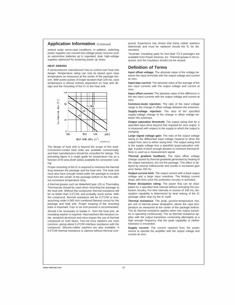
A semiconductor manufacturer has no control over heat sinkdesign. Temperature rating can only be based upon casetemperature as measured at the center of the package bot-tom. With power pulses of longer duration than 100 ms, casetemperature is almost entirely dependent on heat sink de-sign and the mounting of the IC to the heat sink.
The design of heat sink is beyond the scope of this work.Convection-cooled heat sinks are available commercially,and their manufacturers should be consulted for ratings. Thepreceding figure is a rough guide for temperature rise as afunction of fin area (both sides) available for convection cool-ing.
Proper mounting of the IC is required to minimize the thermaldrop between the package and the heat sink. The heat sinkmust also have enough metal under the package to conductheat from the center of the package bottom to the fins with-out excessive temperature drop.
A thermal grease such as Wakefield type 120 or ThermalloyThermacote should be used when mounting the package tothe heat sink. Without this compound, thermal resistance willbe no better than 0.5˚C/W, and probably much worse. Withthe compound, thermal resistance will be 0.2˚C/W or less,assuming under 0.005 inch combined flatness runout for thepackage and heat sink. Proper torquing of the mountingbolts is important. Four to six inch-pounds is recommended.
Should it be necessary to isolate V− from the heat sink, aninsulating washer is required. Hard washers like berylium ox-ide, anodized aluminum and mica require the use of thermalcompound on both faces. Two-mil mica washers are mostcommon, giving about 0.4˚C/W interface resistance with thecompound. Silicone-rubber washers are also available. A0.5˚C/W thermal resistance is claimed without thermal com-
pound. Experience has shown that these rubber washersdeteriorate and must be replaced should the IC be dis-mounted.
“Isostrate” insulating pads for four-lead TO-3 packages areavailable from Power Devices, Inc. Thermal grease is not re-quired, and the insulators should not be reused.
Definition of TermsInput offset voltage: The absolute value of the voltage be-tween the input terminals with the output voltage and currentat zero.
Input bias current: The absolute value of the average of thetwo input currents with the output voltage and current atzero.
Input offset current: The absolute value of the difference inthe two input currents with the output voltage and current atzero.
Common-mode rejection: The ratio of the input voltagerange to the change in offset voltage between the extremes.
Supply-voltage rejection: The ratio of the specifiedsupply-voltage change to the change in offset voltage be-tween the extremes.
Output saturation threshold: The output swing limit for aspecified input drive beyond that required for zero output. Itis measured with respect to the supply to which the output isswinging.
Large signal voltage gain: The ratio of the output voltageswing to the differential input voltage required to drive theoutput from zero to either swing limit. The output swing limitis the supply voltage less a specified quasi-saturation volt-age. A pulse of short enough duration to minimize thermal ef-fects is used as a measurement signal.
Thermal gradient feedback: The input offset voltagechange caused by thermal gradients generated by heating ofthe output transistors, but not the package. This effect is de-layed by several milliseconds and results in increased gainerror below 100 Hz.
Output-current limit: The output current with a fixed outputvoltage and a large input overdrive. The limiting currentdrops with time once the protection circuitry is activated.
Power dissipation rating: The power that can be dissi-pated for a specified time interval without activating the pro-tection circuitry. For time intervals in excess of 100 ms, dis-sipation capability is determined by heat sinking of the ICpackage rather than by the IC itself.
Thermal resistance: The peak, junction-temperature rise,per unit of internal power dissipation, above the case tem-perature as measured at the center of the package bottom.The dc thermal resistance applies when one output transis-tor is operating continuously. The ac thermal resistance ap-plies with the output transistors conducting alternately at ahigh enough frequency that the peak capability of neithertransistor is exceeded.
Supply current: The current required from the powersource to operate the amplifier with the output voltage andcurrent at zero.
DS008704-28
www.national.com 12
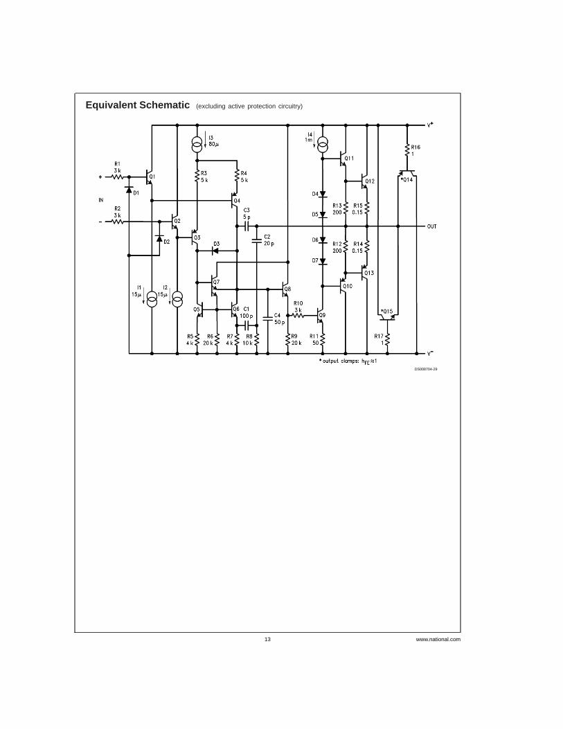
Equivalent Schematic (excluding active protection circuitry)
DS008704-29
www.national.com13
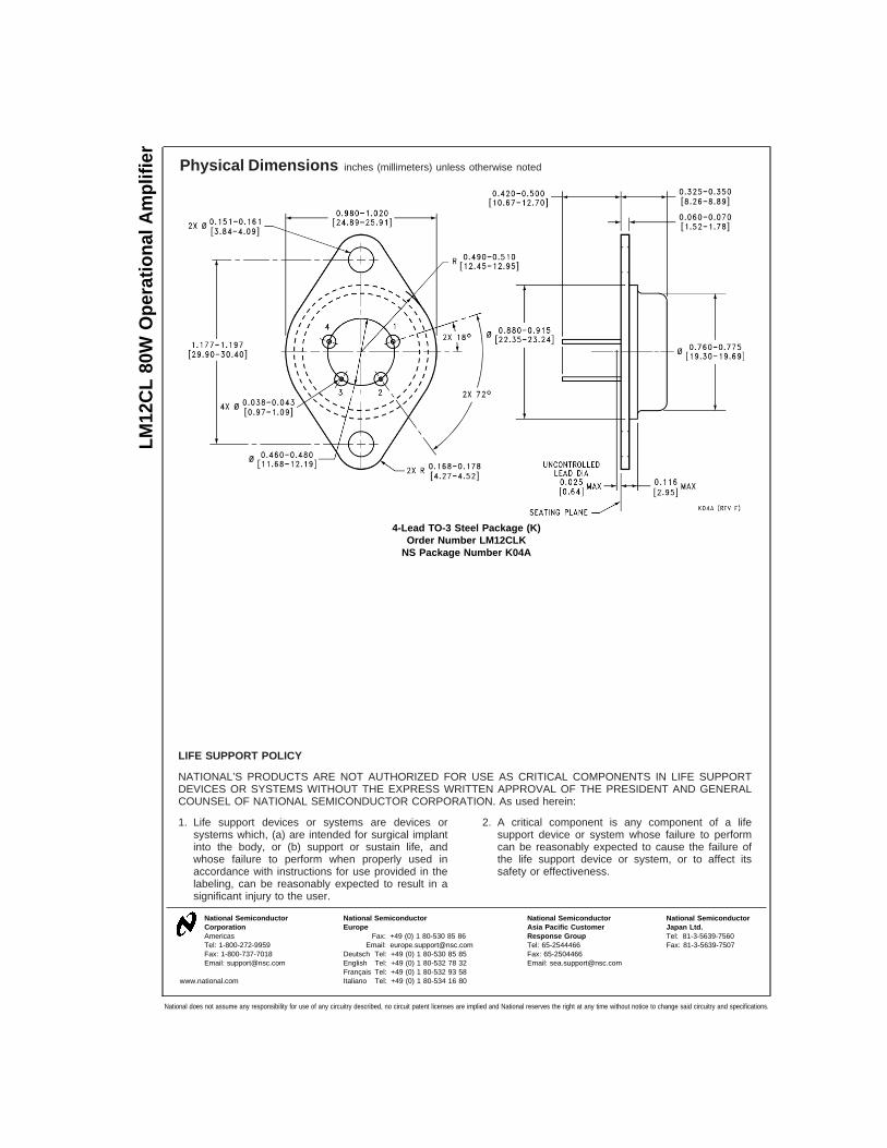
Physical Dimensions inches (millimeters) unless otherwise noted
LIFE SUPPORT POLICY
NATIONAL’S PRODUCTS ARE NOT AUTHORIZED FOR USE AS CRITICAL COMPONENTS IN LIFE SUPPORTDEVICES OR SYSTEMS WITHOUT THE EXPRESS WRITTEN APPROVAL OF THE PRESIDENT AND GENERALCOUNSEL OF NATIONAL SEMICONDUCTOR CORPORATION. As used herein:
1. Life support devices or systems are devices orsystems which, (a) are intended for surgical implantinto the body, or (b) support or sustain life, andwhose failure to perform when properly used inaccordance with instructions for use provided in thelabeling, can be reasonably expected to result in asignificant injury to the user.
2. A critical component is any component of a lifesupport device or system whose failure to performcan be reasonably expected to cause the failure ofthe life support device or system, or to affect itssafety or effectiveness.
National SemiconductorCorporationAmericasTel: 1-800-272-9959Fax: 1-800-737-7018Email: [email protected]
National SemiconductorEurope
Fax: +49 (0) 1 80-530 85 86Email: [email protected]
Deutsch Tel: +49 (0) 1 80-530 85 85English Tel: +49 (0) 1 80-532 78 32Français Tel: +49 (0) 1 80-532 93 58Italiano Tel: +49 (0) 1 80-534 16 80
National SemiconductorAsia Pacific CustomerResponse GroupTel: 65-2544466Fax: 65-2504466Email: [email protected]
National SemiconductorJapan Ltd.Tel: 81-3-5639-7560Fax: 81-3-5639-7507
www.national.com
4-Lead TO-3 Steel Package (K)Order Number LM12CLK
NS Package Number K04A
LM12
CL
80W
Ope
ratio
nalA
mpl
ifier
National does not assume any responsibility for use of any circuitry described, no circuit patent licenses are implied and National reserves the right at any time without notice to change said circuitry and specifications.