lm25115 secondary side post regulator controller (rev. a) · pdf file ·...
TRANSCRIPT
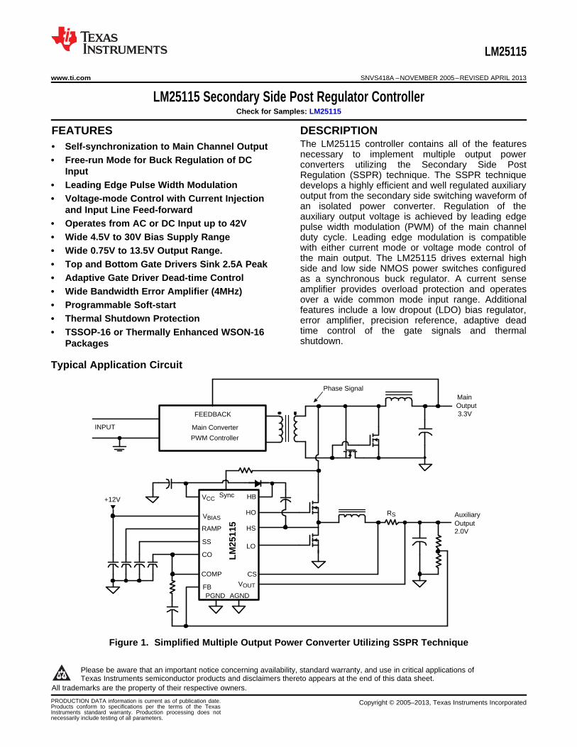
MainOutput3.3V
VBIAS
FBAGND
COMP
SyncVCC
SS
HB
HO
HS
LO
PGND
VOUT
CO
CS
RAMP
LM
2511
5
AuxiliaryOutput2.0V
+12V
RS
FEEDBACK
Main Converter
PWM Controller
INPUT
Phase Signal
LM25115
www.ti.com SNVS418A –NOVEMBER 2005–REVISED APRIL 2013
LM25115 Secondary Side Post Regulator ControllerCheck for Samples: LM25115
1FEATURES DESCRIPTIONThe LM25115 controller contains all of the features
2• Self-synchronization to Main Channel Outputnecessary to implement multiple output power
• Free-run Mode for Buck Regulation of DC converters utilizing the Secondary Side PostInput Regulation (SSPR) technique. The SSPR technique
• Leading Edge Pulse Width Modulation develops a highly efficient and well regulated auxiliaryoutput from the secondary side switching waveform of• Voltage-mode Control with Current Injectionan isolated power converter. Regulation of theand Input Line Feed-forwardauxiliary output voltage is achieved by leading edge
• Operates from AC or DC Input up to 42V pulse width modulation (PWM) of the main channel• Wide 4.5V to 30V Bias Supply Range duty cycle. Leading edge modulation is compatible
with either current mode or voltage mode control of• Wide 0.75V to 13.5V Output Range.the main output. The LM25115 drives external high
• Top and Bottom Gate Drivers Sink 2.5A Peak side and low side NMOS power switches configured• Adaptive Gate Driver Dead-time Control as a synchronous buck regulator. A current sense
amplifier provides overload protection and operates• Wide Bandwidth Error Amplifier (4MHz)over a wide common mode input range. Additional• Programmable Soft-start features include a low dropout (LDO) bias regulator,
• Thermal Shutdown Protection error amplifier, precision reference, adaptive deadtime control of the gate signals and thermal• TSSOP-16 or Thermally Enhanced WSON-16shutdown.Packages
Typical Application Circuit
Figure 1. Simplified Multiple Output Power Converter Utilizing SSPR Technique
1
Please be aware that an important notice concerning availability, standard warranty, and use in critical applications ofTexas Instruments semiconductor products and disclaimers thereto appears at the end of this data sheet.
2All trademarks are the property of their respective owners.
PRODUCTION DATA information is current as of publication date. Copyright © 2005–2013, Texas Instruments IncorporatedProducts conform to specifications per the terms of the TexasInstruments standard warranty. Production processing does notnecessarily include testing of all parameters.
1
2
3
4
5
6
7
8 9
10
CS
HB
HS
SS
VBIAS
PGND
CO
HO
VCC
11
12
13
14
15
16
FB
AGND
VOUT
RAMP SYNC
LO
COMP
LM25115
SNVS418A –NOVEMBER 2005–REVISED APRIL 2013 www.ti.com
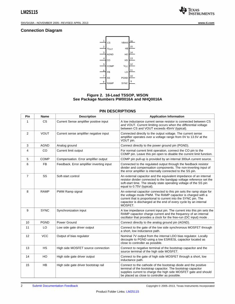
Connection Diagram
Figure 2. 16-Lead TSSOP, WSONSee Package Numbers PW0016A and NHQ0016A
PIN DESCRIPTIONSPin Name Description Application Information
1 CS Current Sense amplifier positive input A low inductance current sense resistor is connected between CSand VOUT. Current limiting occurs when the differential voltagebetween CS and VOUT exceeds 45mV (typical).
2 VOUT Current sense amplifier negative input Connected directly to the output voltage. The current senseamplifier operates over a voltage range from 0V to 13.5V at theVOUT pin.
3 AGND Analog ground Connect directly to the power ground pin (PGND).
4 CO Current limit output For normal current limit operation, connect the CO pin to theCOMP pin. Leave this pin open to disable the current limit function.
5 COMP Compensation. Error amplifier output COMP pin pull-up is provided by an internal 300uA current source.
6 FB Feedback. Error amplifier inverting input Connected to the regulated output through the feedback resistordivider and compensation components. The non-inverting input ofthe error amplifier is internally connected to the SS pin.
7 SS Soft-start control An external capacitor and the equivalent impedance of an internalresistor divider connected to the bandgap voltage reference set thesoft-start time. The steady state operating voltage of the SS pinequal to 0.75V (typical).
8 RAMP PWM Ramp signal An external capacitor connected to this pin sets the ramp slope forthe voltage mode PWM. The RAMP capacitor is charged with acurrent that is proportional to current into the SYNC pin. Thecapacitor is discharged at the end of every cycle by an internalMOSFET.
9 SYNC Synchronization input A low impedance current input pin. The current into this pin sets theRAMP capacitor charge current and the frequency of an internaloscillator that provides a clock for the free-run (DC input) mode .
10 PGND Power Ground Connect directly to the analog ground pin (AGND).
11 LO Low side gate driver output Connect to the gate of the low side synchronous MOSFET througha short, low inductance path.
12 VCC Output of bias regulator Nominal 7V output from the internal LDO bias regulator. Locallydecouple to PGND using a low ESR/ESL capacitor located asclose to controller as possible.
13 HS High side MOSFET source connection Connect to negative terminal of the bootstrap capacitor and thesource terminal of the high side MOSFET.
14 HO High side gate driver output Connect to the gate of high side MOSFET through a short, lowinductance path.
15 HB High side gate driver bootstrap rail Connect to the cathode of the bootstrap diode and the positiveterminal of the bootstrap capacitor. The bootstrap capacitorsupplies current to charge the high side MOSFET gate and shouldbe placed as close to controller as possible.
2 Submit Documentation Feedback Copyright © 2005–2013, Texas Instruments Incorporated
Product Folder Links: LM25115

VBIAS VCC
HB
CS
SYNC
ENABLE
PGND
AGND
LEVELSHIFT
CLK
VOUT
HS
ERROR AMP(Sink Only)
R
S Q
Q
VCC
UVLO
7V LDOREGULATOR
HODRIVER
LODRIVER
RAMP
75k
SS
FB
COMP
PWMCOMPARATOR
CURRENT SENSE AMPGain = 16
CO
NEGATIVECURRENT
DETECTOR
7V
1.27V
2V
40k
100k
0.7V
BUFFER
0.75V
300 PA
ILIMIT AMPGm = 16 mA/V
(Sink Only)
1V
1.27V175k
120k
ADAPTIVEDEAD TIME
DELAY
THERMALLIMIT
LOGIC
CV
2.5k
15 PA
CLK
2.5k
CRMIX
VCC
VCC
VCC
VCCISYNC
Vbias
ISYNC x 3
+-2.3V
LM25115
www.ti.com SNVS418A –NOVEMBER 2005–REVISED APRIL 2013
PIN DESCRIPTIONS (continued)
Pin Name Description Application Information
16 VBIAS Supply Bias Input Input to the LDO bias regulator and current sense amplifier thatpowers internal blocks. Input range of VBIAS is 4.5V to 30V.
- Exposed Pad Exposed Pad, underside of WSON package Internally bonded to the die substrate. Connect to system ground(WSON for low thermal impedance.Package
Only)
Block Diagram
Copyright © 2005–2013, Texas Instruments Incorporated Submit Documentation Feedback 3
Product Folder Links: LM25115
LM25115
SNVS418A –NOVEMBER 2005–REVISED APRIL 2013 www.ti.com
These devices have limited built-in ESD protection. The leads should be shorted together or the device placed in conductive foamduring storage or handling to prevent electrostatic damage to the MOS gates.
ABSOLUTE MAXIMUM RATINGS (1) (2)
VBIAS to GND –0.3V to 32V
VCC to GND –0.3V to 9V
HS to GND –1V to 45V
VOUT, CS to GND – 0.3V to 15V
All other inputs to GND −0.3V to 7.0V
Storage Temperature Range –55°C to +150°C
Junction Temperature +150°C
ESD RatingHBM (3) 2 kV
(1) Absolute Maximum Ratings indicate limits beyond which damage to the component may occur. Operating Ratings are conditions underwhich operation of the device is specified. Operating Ratings do not imply ensured performance limits. For ensured performance limitsand associated test conditions, see the Electrical Characteristics tables.
(2) If Military/Aerospace specified devices are required, please contact the Texas Instruments Sales Office/Distributors for availability andspecifications.
(3) The human body model is a 100 pF capacitor discharged through a 1.5kΩ resistor into each pin.
OPERATING RATINGSVBIAS supply voltage 5V to 30V
VCC supply voltage 5V to 7.5V
HS voltage 0V to 42V
HB voltage VCC + HS
Operating Junction Temperature –40°C to +125°C
TYPICAL OPERATING CONDITIONSParameter Min Typ Max Units
Supply Voltage, VBIAS 4.5 30 V
Supply Voltage, VCC 4.5 7 V
Supply voltage bypass, CVBIAS 0.1 1 µF
Reference bypass capacitor, CVCC 0.1 1 10 µF
HB-HS bootstrap capacitor 0.047 µF
SYNC Current Range (VCC = 4.5V) 50 150 µA
RAMP Saw Tooth Amplitude 1 1.75 V
VOUT regulation voltage (VBIAS min = 3V + VOUT) 0.75 13.5 V
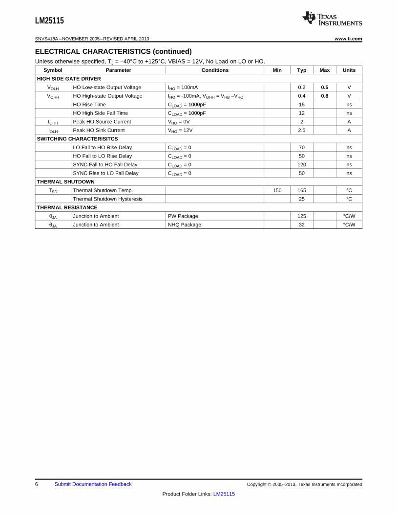
ELECTRICAL CHARACTERISTICSUnless otherwise specified, TJ = –40°C to +125°C, VBIAS = 12V, No Load on LO or HO.
Symbol Parameter Conditions Min Typ Max Units
VBIAS SUPPLY
Ibias VBIAS Supply Current FSYNC = 200kHz 4 mA
VCC LOW DROPOUT BIAS REGULATOR
VccReg VCC Regulation VCC open circuit. Outputs not switching 6.65 7 7.15 V
VCC Current Limit ( (1)) 40 mA
VCC Under-voltage Lockout Voltage Positive going VCC 4 4.5 V
VCC Under-voltage Hysteresis 0.2 0.25 0.3 V
(1) Device thermal limitations may limit usable range.
4 Submit Documentation Feedback Copyright © 2005–2013, Texas Instruments Incorporated
Product Folder Links: LM25115
LM25115
www.ti.com SNVS418A –NOVEMBER 2005–REVISED APRIL 2013
ELECTRICAL CHARACTERISTICS (continued)Unless otherwise specified, TJ = –40°C to +125°C, VBIAS = 12V, No Load on LO or HO.
Symbol Parameter Conditions Min Typ Max Units
SOFT-START
SS Source Impedance 43 60 77 kΩSS Discharge Impedance 100 Ω
ERROR AMPLIFIER and FEEDBACK REFERENCE
VREF FB Reference Voltage Measured at FB pin 0.737 0.75 0.763 V
FB Input Bias Current FB = 2V 0.2 0.5 µA
COMP Source Current 300 µA
Open Loop Voltage Gain 60 dB
GBW Gain Bandwidth Product 4 MHz
Vio Input Offset Voltage -7 0 7 mV
COMP Offset Threshold for VHO = high RAMP = CS = 2 VVOUT = 0V
RAMP Offset Threshold for VHO = high COMP = 1.5V, 1.1 VCS = VOUT = 0V
CURRENT SENSE AMPLIFIER
Current Sense Amplifier Gain 16 V/V
Output DC Offset 1.27 V
Amplifier Bandwidth 500 kHz
CURRENT LIMIT
ILIMIT Amp Transconductance 16 mA / V
Overall Transconductance 237 mA / V
Positive Current Limit VCL = VCS - VVOUT 37 45 53 mVVOUT = 6V and CO/COMP = 1.5V
Positive Current Limit Foldback VCL = VCS - VVOUT 31 38 45 mVVOUT = 0V and CO/COMP = 1.5V
VCLneg Negative Current Limit VOUT = 6V -17 mVVCL = VCS - VVOUT to cause LO toshutoff
RAMP GENERATOR
SYNC Input Impedance 2.5 kΩSYNC Threshold End of cycle detection threshold 15 µA
Free Run Mode Peak Threshold RAMP peak voltage with dc current 2.3 Vapplied to SYNC.
Current Mirror Gain Ratio of RAMP charge current to SYNC 2.7 3.3 A/Ainput current.
Discharge Impedance 100 ΩLOW SIDE GATE DRIVER
VOLL LO Low-state Output Voltage ILO = 100mA 0.2 0.5 V
VOHL LO High-state Output Voltage ILO = -100mA, VOHL = VCC -VLO 0.4 0.8 V
LO Rise Time CLOAD = 1000pF 15 ns
LO Fall Time CLOAD = 1000pF 12 ns
IOHL Peak LO Source Current VLO = 0V 2 A
IOLL Peak LO Sink Current VLO = 12V 2.5 A
Copyright © 2005–2013, Texas Instruments Incorporated Submit Documentation Feedback 5
Product Folder Links: LM25115
LM25115
SNVS418A –NOVEMBER 2005–REVISED APRIL 2013 www.ti.com
ELECTRICAL CHARACTERISTICS (continued)Unless otherwise specified, TJ = –40°C to +125°C, VBIAS = 12V, No Load on LO or HO.
Symbol Parameter Conditions Min Typ Max Units
HIGH SIDE GATE DRIVER
VOLH HO Low-state Output Voltage IHO = 100mA 0.2 0.5 V
VOHH HO High-state Output Voltage IHO = -100mA, VOHH = VHB –VHO 0.4 0.8 V
HO Rise Time CLOAD = 1000pF 15 ns
HO High Side Fall Time CLOAD = 1000pF 12 ns
IOHH Peak HO Source Current VHO = 0V 2 A
IOLH Peak HO Sink Current VHO = 12V 2.5 A
SWITCHING CHARACTERISITCS
LO Fall to HO Rise Delay CLOAD = 0 70 ns
HO Fall to LO Rise Delay CLOAD = 0 50 ns
SYNC Fall to HO Fall Delay CLOAD = 0 120 ns
SYNC Rise to LO Fall Delay CLOAD = 0 50 ns
THERMAL SHUTDOWN
TSD Thermal Shutdown Temp. 150 165 °C
Thermal Shutdown Hysteresis 25 °C
THERMAL RESISTANCE
θJA Junction to Ambient PW Package 125 °C/W
θJA Junction to Ambient NHQ Package 32 °C/W
6 Submit Documentation Feedback Copyright © 2005–2013, Texas Instruments Incorporated
Product Folder Links: LM25115

100 1K 10K 100K 1M
FREQUENCY (Hz)
GA
IN (
dB)
0
5
10
15
20
25
PH
AS
E (
o )
-70
-55
-40
-25
-10
5Gain
Phase
16 V/V
Offset 1.27V
CV
(V
)
-20 -10 0 10 20 30 40 50 60
VCL (mV)
0
0.5
1
1.5
2
2.5VOUT = 6V
0 2 4 6 8 10 12 14 16
VBIAS (V)
0
2
4
6
8
10
12
14
16
VC
C (
V)
VBIAS
VCC
VC
C (
V)
ICC (mA)
0 5 10 15 20 25 30 35 40 450
1
2
3
4
5
6
7
8
LM25115
www.ti.com SNVS418A –NOVEMBER 2005–REVISED APRIL 2013
TYPICAL PERFORMANCE CHARACTERISTICS
VCC Regulator Start-Up Characteristics, VCCvs
VBIAS VCC Load Regulation to Current Limit
Figure 3. Figure 4.
Current Value (CV) Current Sense Amplifier Gain and Phasevs vs
Current Limit (VCL) Frequency
Figure 5. Figure 6.
Copyright © 2005–2013, Texas Instruments Incorporated Submit Documentation Feedback 7
Product Folder Links: LM25115
125oC
0 10 20 30 40 500
2
4
6
8
10
12
14
VO
UT (
V)
VCL (mV)
27oC
-40oC
-20 -19 -18 -17 -16 -150
2
4
6
8
10
12
VO
UT (
V)
VCL (mV)
VCL (mV)
0
50
100
150
200
250
300
350
400
I CO
(P
A)
30 35 40 45 50
237 mA/V
VOUT = 6V
1.99 1.995 2 2.005 2.01 2.015 2.02
CV (V)
0
50
100
150
200
250
300
350
400I C
O (P
A)
16 mA/V
VOUT = 6V
LM25115
SNVS418A –NOVEMBER 2005–REVISED APRIL 2013 www.ti.com
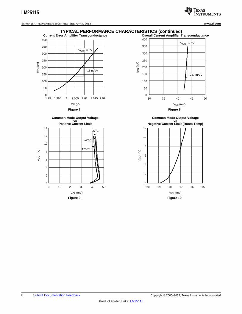
TYPICAL PERFORMANCE CHARACTERISTICS (continued)Current Error Amplifier Transconductance Overall Current Amplifier Transconductance
Figure 7. Figure 8.
Common Mode Output Voltage Common Mode Output Voltagevs vs
Positive Current Limit Negative Current Limit (Room Temp)
Figure 9. Figure 10.
8 Submit Documentation Feedback Copyright © 2005–2013, Texas Instruments Incorporated
Product Folder Links: LM25115
SYNC CLK
RAMP
BUFFER
2.5K
15 PA
CLK
Isync
Isync x 3
2.5k
PhaseSignal
R SYNC
CRAMP
LM25115
www.ti.com SNVS418A –NOVEMBER 2005–REVISED APRIL 2013
DETAILED OPERATING DESCRIPTION
The LM25115 controller contains all of the features necessary to implement multiple output power convertersutilizing the Secondary Side Post Regulation (SSPR) technique. The SSPR technique develops a highly efficientand well regulated auxiliary output from the secondary side switching waveform of an isolated power converter.Regulation of the auxiliary output voltage is achieved by leading edge pulse width modulation (PWM) of the mainchannel duty cycle. Leading edge modulation is compatible with either current mode or voltage mode control ofthe main output. The LM25115 drives external high side and low side NMOS power switches configured as asynchronous buck regulator. A current sense amplifier provides overload protection and operates over a widecommon mode input range from 0V to 13.5V. Additional features include a low dropout (LDO) bias regulator,error amplifier, precision reference, adaptive dead time control of the gate driver signals and thermal shutdown. Aprogrammable oscillator provides a PWM clock signal when the LM25115 is powered by a dc input (free-runmode) instead of the phase signal of the main channel converter (SSPR mode).
Low Drop-out Bias Regulator (VCC)
The LM25115 contains an internal LDO regulator that operates over an input supply range from 4.5V to 30V. Theoutput of the regulator at the VCC pin is nominally regulated at 7V and is internally current limited to 40mA. VCCis the main supply to the internal logic, PWM controller, and gate driver circuits. When power is applied to theVBIAS pin, the regulator is enabled and sources current into an external capacitor connected to the VCC pin.The recommended output capacitor range for the VCC regulator is 0.1uF to 100uF. When the voltage at the VCCpin reaches the VCC under-voltage lockout threshold of 4.25V, the controller is enabled. The controller isdisabled if VCC falls below 4.0V (250mV hysteresis). In applications where an appropriate regulated dc biassupply is available, the LM25115 controller can be powered directly through the VCC pin instead of the VBIASpin. In this configuration, it is recommended that the VCC and the VBIAS pins be connected together such thatthe external bias voltage is applied to both pins. The allowable VCC range when biased from an external supplyis 4.5V to 7V.
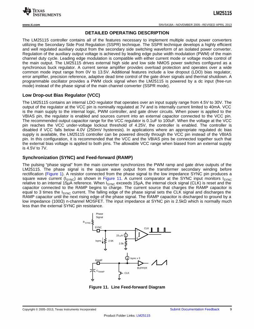
Synchronization (SYNC) and Feed-forward (RAMP)
The pulsing “phase signal” from the main converter synchronizes the PWM ramp and gate drive outputs of theLM25115. The phase signal is the square wave output from the transformer secondary winding beforerectification (Figure 1). A resistor connected from the phase signal to the low impedance SYNC pin produces asquare wave current (ISYNC) as shown in Figure 11. A current comparator at the SYNC input monitors ISYNCrelative to an internal 15µA reference. When ISYNC exceeds 15µA, the internal clock signal (CLK) is reset and thecapacitor connected to the RAMP begins to charge. The current source that charges the RAMP capacitor isequal to 3 times the ISYNC current. The falling edge of the phase signal sets the CLK signal and discharges theRAMP capacitor until the next rising edge of the phase signal. The RAMP capacitor is discharged to ground by alow impedance (100Ω) n-channel MOSFET. The input impedance at SYNC pin is 2.5kΩ which is normally muchless than the external SYNC pin resistance.
Figure 11. Line Feed-forward Diagram
Copyright © 2005–2013, Texas Instruments Incorporated Submit Documentation Feedback 9
Product Folder Links: LM25115

Phase signal
RAMP pin
HS pin
12V
12V
6V
6V
Main Output = 3.3V
Secondary Output = 2.5V
PWM Threshold
LM25115
SNVS418A –NOVEMBER 2005–REVISED APRIL 2013 www.ti.com
The RAMP and SYNC functions illustrated in Figure 11 provide line voltage feed-forward to improve theregulation of the auxiliary output when the input voltage of the main converter changes. Varying the input voltageto the main converter produces proportional variations in amplitude of the phase signal. The main channel PWMcontroller adjusts the pulse width of the phase signal to maintain constant volt*seconds and a regulated mainoutput as shown in Figure 12. The variation of the phase signal amplitude and duration are reflected in the slopeand duty cycle of the RAMP signal of the LM25115 (ISYNC α phase signal amplitude). As a result, the duty cycleof the LM25115 is automatically adjusted to regulate the auxiliary output voltage with virtually no change in thePWM threshold voltage. Transient line regulation is improved because the PWM duty cycle of the auxiliaryconverter is immediately corrected, independent of the delays of the voltage regulation loop.
Figure 12. Line Feed-forward Waveforms
The recommended SYNC input current range is 50µA to 150µA. The SYNC pin resistor (RSYNC) should beselected to set the SYNC current (ISYNC) to 150µA with the maximum phase signal amplitude, VPHASE(max). Thiswill ensure that ISYNC stays within the recommended range over a 3:1 change in phase signal amplitude. TheSYNC pin resistor is therefore:
RSYNC = (VPHASE(max) / 150µA) - 2.5kΩ
Once ISYNC has been established by selecting RSYNC, the RAMP signal amplitude may be programmed byselecting the proper RAMP pin capacitor value. The recommended peak amplitude of the RAMP waveform is 1Vto 1.75V. The CRAMP capacitor is chosen to provide the desired RAMP amplitude with the nominal phase signalvoltage and pulse width.
CRAMP = (3 x ISYNC x TON ) / VRAMP
where• CRAMP = RAMP pin capacitance• ISYNC = SYNC pin current current• TON = corresponding phase signal pulse width• VRAMP = desired RAMP amplitude (1V to 1.75V)
For example,
Main channel output = 3.3V. Phase signal maximum amplitude = 12V. Phase signal frequency = 250kHz• Set ISYNC = 150µA with phase signal at maximum amplitude (12V):
– ISYNC = 150µA = VPHASE(max) / (RSYNC + 2.5 kΩ) = 12V / (RSYNC + 2.5 kΩ)– RSYNC = 12V/150µA - 2.5kΩ = 77.5kΩ
• TON = Main channel duty cycle / Phase frequency = (3.3V/12V) / 250kHz = 1.1µs• Assume desired VRAMP = 1.5V• CRAMP = (3 x ISYNC x TON ) / VRAMP = (3 x 150µA x 1.1µs) / 1.5V• CRAMP = 330pF
10 Submit Documentation Feedback Copyright © 2005–2013, Texas Instruments Incorporated
Product Folder Links: LM25115

CRMIX
HS
Phase or CLK
Leading Edge Modulation
CV
RAMP
ERRORAMP
RAMP
75K
SS
FB
COMP
PWM
40k
100k
0.7V
0.75V
CLK
Isync x 3
CRMIX
CV
BUFFERCRAMP
LM25115
www.ti.com SNVS418A –NOVEMBER 2005–REVISED APRIL 2013
Error Amplifier and Soft-Start (FB, CO, & COMP, SS)
An internal wide bandwidth error amplifier is provided within the LM25115 for voltage feedback to the PWMcontroller. The amplifier’s inverting input is connected to the FB pin. The output of the auxiliary converter isregulated by connecting a voltage setting resistor divider between the output and the FB pin. Loop compensationnetworks are connected between the FB pin and the error amplifier output (COMP). The amplifier’s non-invertinginput is internally connected to the SS pin. The SS pin is biased at 0.75V by a resistor divider connected to theinternal 1.27V bandgap reference. When the VCC voltage is below the UVLO threshold, the SS pin is dischargedto ground. When VCC rises and exceeds the positive going UVLO threshold (4.25V), the SS pin is released andallowed to rise. If an external capacitor is connected to the SS pin, it will be charged by the internal resistordivider to gradually increase the non-inverting input of the error amplifier to 0.75V. The equivalent impedance ofthe SS resistor divider is nominally 60kΩ which determines the charging time constant of the SS capacitor.During start-up, the output of the LM25115 converter will follow the exponential equation:
VOUT(t) = VOUT(final) x (1 - exp(-t/RSS x CSS))
where• Rss = internal resistance of SS pin (60kΩ)• Css = external Soft-Start capacitor• VOUT(final) = regulator output set point
The initial Δv / Δt of the output voltage is VOUT(final) / Rss x Css and VOUT will be within 1% of the finalregulation level after 4.6 time constants or when t = 4.6 x Rss x Css.
Pull-up current for the error amplifier output is provided by an internal 300µA current source. The PWM thresholdsignal at the COMP pin can be controlled by either the open drain error amplifier or the open drain currentamplifier connected through the CO pin to COMP. Since the internal error amplifier is configured as an opendrain output it can be disabled by connecting FB to ground. The current sense amplifier and current limitingfunction will be described in a later section.
Leading Edge Pulse Width Modulation
Unlike conventional voltage mode controllers, the LM25115 implements leading edge pulse width modulation. Acurrent source equal to 3 times the ISYNC current is used to charge the capacitor connected to the RAMP pin asshown in Figure 13. The ramp signal and the output of the error amplifier (COMP) are combined through aresistor network to produce a voltage ramp with variable dc offset (CRMIX in Figure 13). The high side MOSFETwhich drives the HS pin is held in the off state at the beginning of the phase signal. When the voltage of CRMIXexceeds the internal threshold voltage CV, the PWM comparator turns on the high side MOSFET. The HS pinrises and the MOSFET delivers current from the main converter phase signal to the output of the auxiliaryregulator. The PWM cycle ends when the phase signal falls and power is no longer supplied to the drain of thehigh side MOSFET.
Figure 13. Synchronization and Leading Edge Modulation
Copyright © 2005–2013, Texas Instruments Incorporated Submit Documentation Feedback 11
Product Folder Links: LM25115
Main PWM
Auxilary PWM
TransformerCurrent
Trailing EdgeModulation
Leading EdgeModulation
Peak CurrentThreshold
Peak CurrentThreshold
Main PWM
Auxilary PWM
TransformerCurrent
LM25115
SNVS418A –NOVEMBER 2005–REVISED APRIL 2013 www.ti.com
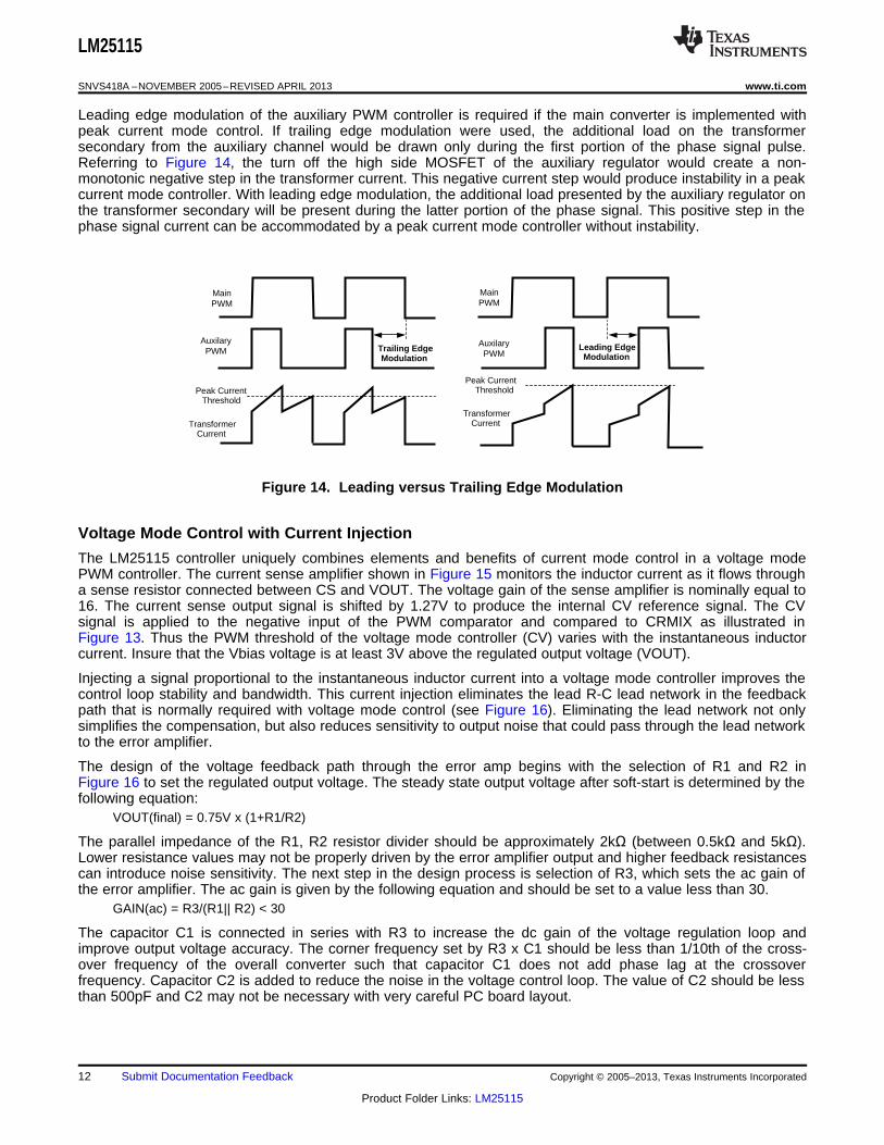
Leading edge modulation of the auxiliary PWM controller is required if the main converter is implemented withpeak current mode control. If trailing edge modulation were used, the additional load on the transformersecondary from the auxiliary channel would be drawn only during the first portion of the phase signal pulse.Referring to Figure 14, the turn off the high side MOSFET of the auxiliary regulator would create a non-monotonic negative step in the transformer current. This negative current step would produce instability in a peakcurrent mode controller. With leading edge modulation, the additional load presented by the auxiliary regulator onthe transformer secondary will be present during the latter portion of the phase signal. This positive step in thephase signal current can be accommodated by a peak current mode controller without instability.
Figure 14. Leading versus Trailing Edge Modulation
Voltage Mode Control with Current Injection
The LM25115 controller uniquely combines elements and benefits of current mode control in a voltage modePWM controller. The current sense amplifier shown in Figure 15 monitors the inductor current as it flows througha sense resistor connected between CS and VOUT. The voltage gain of the sense amplifier is nominally equal to16. The current sense output signal is shifted by 1.27V to produce the internal CV reference signal. The CVsignal is applied to the negative input of the PWM comparator and compared to CRMIX as illustrated inFigure 13. Thus the PWM threshold of the voltage mode controller (CV) varies with the instantaneous inductorcurrent. Insure that the Vbias voltage is at least 3V above the regulated output voltage (VOUT).
Injecting a signal proportional to the instantaneous inductor current into a voltage mode controller improves thecontrol loop stability and bandwidth. This current injection eliminates the lead R-C lead network in the feedbackpath that is normally required with voltage mode control (see Figure 16). Eliminating the lead network not onlysimplifies the compensation, but also reduces sensitivity to output noise that could pass through the lead networkto the error amplifier.
The design of the voltage feedback path through the error amp begins with the selection of R1 and R2 inFigure 16 to set the regulated output voltage. The steady state output voltage after soft-start is determined by thefollowing equation:
VOUT(final) = 0.75V x (1+R1/R2)
The parallel impedance of the R1, R2 resistor divider should be approximately 2kΩ (between 0.5kΩ and 5kΩ).Lower resistance values may not be properly driven by the error amplifier output and higher feedback resistancescan introduce noise sensitivity. The next step in the design process is selection of R3, which sets the ac gain ofthe error amplifier. The ac gain is given by the following equation and should be set to a value less than 30.
GAIN(ac) = R3/(R1|| R2) < 30
The capacitor C1 is connected in series with R3 to increase the dc gain of the voltage regulation loop andimprove output voltage accuracy. The corner frequency set by R3 x C1 should be less than 1/10th of the cross-over frequency of the overall converter such that capacitor C1 does not add phase lag at the crossoverfrequency. Capacitor C2 is added to reduce the noise in the voltage control loop. The value of C2 should be lessthan 500pF and C2 may not be necessary with very careful PC board layout.
12 Submit Documentation Feedback Copyright © 2005–2013, Texas Instruments Incorporated
Product Folder Links: LM25115
ERRORAMP
SS
FB
40k
100k0.75V
60k
R1
R2
R3
CSS
C2C1
PWM
VOUT
COMP
CV
No LeadNetworkRequired
CS
VOUT
Current Sense Amp
1.27V
CV
CO
Gm = 15 mA/V
Negative Current Comparator
1V
Current Limit Amp
2V
PWMComparator
CRMIX to PWMLatch
Low Side Enable
= 16AV
VCL
Vbias
LM25115
www.ti.com SNVS418A –NOVEMBER 2005–REVISED APRIL 2013
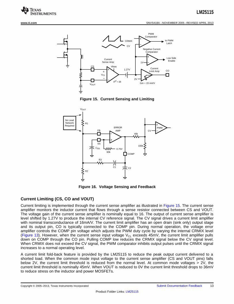
Figure 15. Current Sensing and Limiting
Figure 16. Voltage Sensing and Feedback
Current Limiting (CS, CO and VOUT)
Current limiting is implemented through the current sense amplifier as illustrated in Figure 15. The current senseamplifier monitors the inductor current that flows through a sense resistor connected between CS and VOUT.The voltage gain of the current sense amplifier is nominally equal to 16. The output of current sense amplifier islevel shifted by 1.27V to produce the internal CV reference signal. The CV signal drives a current limit amplifierwith nominal transconductance of 16mA/V. The current limit amplifier has an open drain (sink only) output stageand its output pin, CO is typically connected to the COMP pin. During normal operation, the voltage erroramplifier controls the COMP pin voltage which adjusts the PWM duty cycle by varying the internal CRMIX level(Figure 13). However, when the current sense input voltage VCL exceeds 45mV, the current limit amplifier pullsdown on COMP through the CO pin. Pulling COMP low reduces the CRMIX signal below the CV signal level.When CRMIX does not exceed the CV signal, the PWM comparator inhibits output pulses until the CRMIX signalincreases to a normal operating level.
A current limit fold-back feature is provided by the LM25115 to reduce the peak output current delivered to ashorted load. When the common mode input voltage to the current sense amplifier (CS and VOUT pins) fallsbelow 2V, the current limit threshold is reduced from the normal level. At common mode voltages > 2V, thecurrent limit threshold is nominally 45mV. When VOUT is reduced to 0V the current limit threshold drops to 36mVto reduce stress on the inductor and power MOSFETs.
Copyright © 2005–2013, Texas Instruments Incorporated Submit Documentation Feedback 13
Product Folder Links: LM25115

LM25115
SNVS418A –NOVEMBER 2005–REVISED APRIL 2013 www.ti.com
Negative Current Limit
When inductor current flows from the regulator output through the low side MOSFET, the input to the currentsense comparator becomes negative. The intent of the negative current comparator is to protect the low-sideMOSFET from excessive currents. Negative current can lead to large negative voltage spikes on the output atturn off which can damage circuitry powered by the output. The negative current comparator threshold issufficiently negative to allow inductor current to reverse at no load or light load conditions. It is not intended tosupport discontinuous conduction mode with diode emulation by the low-side MOSFET. The negative currentcomparator illustrated in Figure 15 monitors the CV signal and compares this signal to a fixed 1V threshold. Thiscorresponds to a negative VCL voltage between CS and VOUT of -17mV. The negative current limit comparatorturns off the low-side MOSFET for the remainder of the cycle when the VCL input falls below this threshold.
Gate Drivers Outputs (HO & LO)
The LM25115 provides two gate driver outputs, the floating high-side gate driver HO and the synchronousrectifier low-side driver LO. The low-side driver is powered directly by the VCC regulator. The high-side gatedriver is powered from a bootstrap capacitor connected between HB and HS. An external diode connectedbetween VCC and HB charges the bootstrap capacitor when the HS is low. When the high-side MOSFET isturned on, HB rises with HS to a peak voltage equal to VCC + VHS - VD where VD is the forward drop of theexternal bootstrap diode. Both output drivers have adaptive dead-time control to avoid shoot through currents.The adaptive dead-time control circuit monitors the state of each driver to ensure that the opposing MOSFET isturned off before the other is turned on. The HB and VCC capacitors should be placed close to the pins of theLM25115 to minimize voltage transients due to parasitic inductances and the high peak output currents of thedrivers. The recommended range of the HB capacitor is 0.047µF to 0.22µF.
Both drivers are controlled by the PWM logic signal from the PWM latch. When the phase signal is low, theoutputs are held in the reset state with the low-side MOSFET on and the high-side MOSFET off. When the phasesignal switches to the high state, the PWM latch reset signal is de-asserted. The high-side MOSFET remains offuntil the PWM latch is set by the PWM comparator (CRMIX > CV as shown in Figure 13). When the PWM latchis set, the LO driver turns off the low-side MOSFET and the HO driver turns on the high-side MOSFET. The high-side pulse is terminated when the phase signal falls and the SYNC input comparator resets the PWM latch.
Free-Run Mode
The LM25115 can be operated as a conventional synchronous buck controller with a dc input supply instead ofthe square wave phase signal. In the dc or free-run mode, the LM25115 PWM controller synchronizes to aninternal clock signal instead of the phase signal pulses. The clock frequency in the free-run mode is programmedby the SYNC pin resistor and RAMP pin capacitor. Connecting a resistor between a dc bias supply and theSYNC pin produces a current ISYNC which controls the charging current of the RAMP pin capacitor . The RAMPcapacitor is charged until its voltage reaches the free-run mode peak threshold of 2.25V. The RAMP capacitor isthen discharged for 300ns before beginning a new PWM cycle. The 300ns reset time of the RAMP pin sets theminimum off time of the PWM controller in the free-run mode. The internal clock frequency in the free-run modeis set by the synchronization current, ramp capacitor, free-run peak threshold, and 300ns deadtime.
FCLK ≊ 1 / ((CRAMP x 2.25V) / (ISYNC x 3) + 300ns)
Note that the VCC supply can be used as the dc bias to produce ISYNC. Note that the input voltage feedforward isno longer functional in this operating mode, so the loop gain will vary as a function of Vin. The LM25115 controlsthe buck power stage with leading edge pulse width modulaton to hold off the high-side driver until the necessaryvolt*seconds is established for regulation. Other features described for the secondary side post regulator apply inthe free run mode operation. They include voltage mode control with current injection, positive and negativecurrent limit, programmable soft-start, adaptive delays for outputs, and thermal protection.
Thermal Protection
Internal thermal shutdown circuitry is provided to protect the integrated circuit in the event the maximum junctiontemperature limit is exceeded. When activated, typically at 165 degrees Celsius, the controller is forced into a lowpower standby state with the output drivers and the bias regulator disabled. The device will restart when thejunction temperature falls below the thermal shutdown hysteresis, which is typically 25 degrees. The thermalprotection feature is provided to prevent catastrophic failures from accidental device overheating.
14 Submit Documentation Feedback Copyright © 2005–2013, Texas Instruments Incorporated
Product Folder Links: LM25115
LM25115
www.ti.com SNVS418A –NOVEMBER 2005–REVISED APRIL 2013
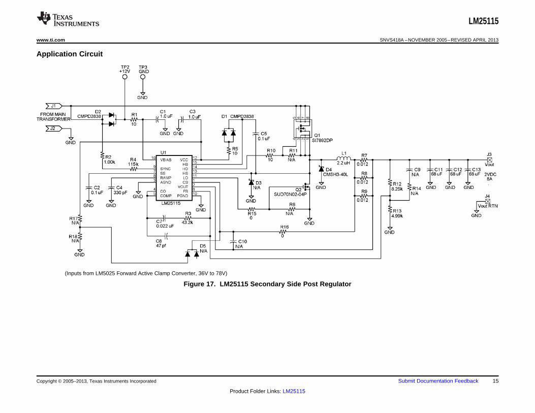
Application Circuit
(Inputs from LM5025 Forward Active Clamp Converter, 36V to 78V)
Figure 17. LM25115 Secondary Side Post Regulator
Copyright © 2005–2013, Texas Instruments Incorporated Submit Documentation Feedback 15
Product Folder Links: LM25115
LM25115
SNVS418A –NOVEMBER 2005–REVISED APRIL 2013 www.ti.com
REVISION HISTORY
Changes from Original (March 2013) to Revision A Page
• Changed layout of National Data Sheet to TI format .......................................................................................................... 14
16 Submit Documentation Feedback Copyright © 2005–2013, Texas Instruments Incorporated
Product Folder Links: LM25115

PACKAGE OPTION ADDENDUM
www.ti.com 27-Oct-2016
Addendum-Page 1
PACKAGING INFORMATION
Orderable Device Status(1)
Package Type PackageDrawing
Pins PackageQty
Eco Plan(2)
Lead/Ball Finish(6)
MSL Peak Temp(3)
Op Temp (°C) Device Marking(4/5)
Samples
LM25115MT/NOPB ACTIVE TSSOP PW 16 92 Green (RoHS& no Sb/Br)
CU SN Level-1-260C-UNLIM -40 to 125 L25115MT
LM25115MTX/NOPB ACTIVE TSSOP PW 16 2500 Green (RoHS& no Sb/Br)
CU SN Level-1-260C-UNLIM -40 to 125 L25115MT
LM25115SDX/NOPB ACTIVE WSON NHQ 16 4500 Green (RoHS& no Sb/Br)
CU SN Level-1-260C-UNLIM -40 to 125 L25115
(1) The marketing status values are defined as follows:ACTIVE: Product device recommended for new designs.LIFEBUY: TI has announced that the device will be discontinued, and a lifetime-buy period is in effect.NRND: Not recommended for new designs. Device is in production to support existing customers, but TI does not recommend using this part in a new design.PREVIEW: Device has been announced but is not in production. Samples may or may not be available.OBSOLETE: TI has discontinued the production of the device.
(2) Eco Plan - The planned eco-friendly classification: Pb-Free (RoHS), Pb-Free (RoHS Exempt), or Green (RoHS & no Sb/Br) - please check http://www.ti.com/productcontent for the latest availabilityinformation and additional product content details.TBD: The Pb-Free/Green conversion plan has not been defined.Pb-Free (RoHS): TI's terms "Lead-Free" or "Pb-Free" mean semiconductor products that are compatible with the current RoHS requirements for all 6 substances, including the requirement thatlead not exceed 0.1% by weight in homogeneous materials. Where designed to be soldered at high temperatures, TI Pb-Free products are suitable for use in specified lead-free processes.Pb-Free (RoHS Exempt): This component has a RoHS exemption for either 1) lead-based flip-chip solder bumps used between the die and package, or 2) lead-based die adhesive used betweenthe die and leadframe. The component is otherwise considered Pb-Free (RoHS compatible) as defined above.Green (RoHS & no Sb/Br): TI defines "Green" to mean Pb-Free (RoHS compatible), and free of Bromine (Br) and Antimony (Sb) based flame retardants (Br or Sb do not exceed 0.1% by weightin homogeneous material)
(3) MSL, Peak Temp. - The Moisture Sensitivity Level rating according to the JEDEC industry standard classifications, and peak solder temperature.
(4) There may be additional marking, which relates to the logo, the lot trace code information, or the environmental category on the device.
(5) Multiple Device Markings will be inside parentheses. Only one Device Marking contained in parentheses and separated by a "~" will appear on a device. If a line is indented then it is a continuationof the previous line and the two combined represent the entire Device Marking for that device.
(6) Lead/Ball Finish - Orderable Devices may have multiple material finish options. Finish options are separated by a vertical ruled line. Lead/Ball Finish values may wrap to two lines if the finishvalue exceeds the maximum column width.
Important Information and Disclaimer:The information provided on this page represents TI's knowledge and belief as of the date that it is provided. TI bases its knowledge and belief on informationprovided by third parties, and makes no representation or warranty as to the accuracy of such information. Efforts are underway to better integrate information from third parties. TI has taken and

PACKAGE OPTION ADDENDUM
www.ti.com 27-Oct-2016
Addendum-Page 2
continues to take reasonable steps to provide representative and accurate information but may not have conducted destructive testing or chemical analysis on incoming materials and chemicals.TI and TI suppliers consider certain information to be proprietary, and thus CAS numbers and other limited information may not be available for release.
In no event shall TI's liability arising out of such information exceed the total purchase price of the TI part(s) at issue in this document sold by TI to Customer on an annual basis.
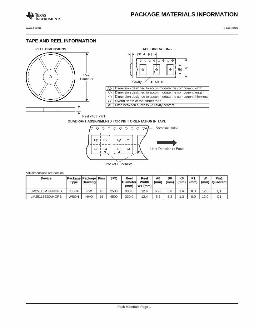
TAPE AND REEL INFORMATION
*All dimensions are nominal
Device PackageType
PackageDrawing
Pins SPQ ReelDiameter
(mm)
ReelWidth
W1 (mm)
A0(mm)
B0(mm)
K0(mm)
P1(mm)
W(mm)
Pin1Quadrant
LM25115MTX/NOPB TSSOP PW 16 2500 330.0 12.4 6.95 5.6 1.6 8.0 12.0 Q1
LM25115SDX/NOPB WSON NHQ 16 4500 330.0 12.4 5.3 5.3 1.3 8.0 12.0 Q1
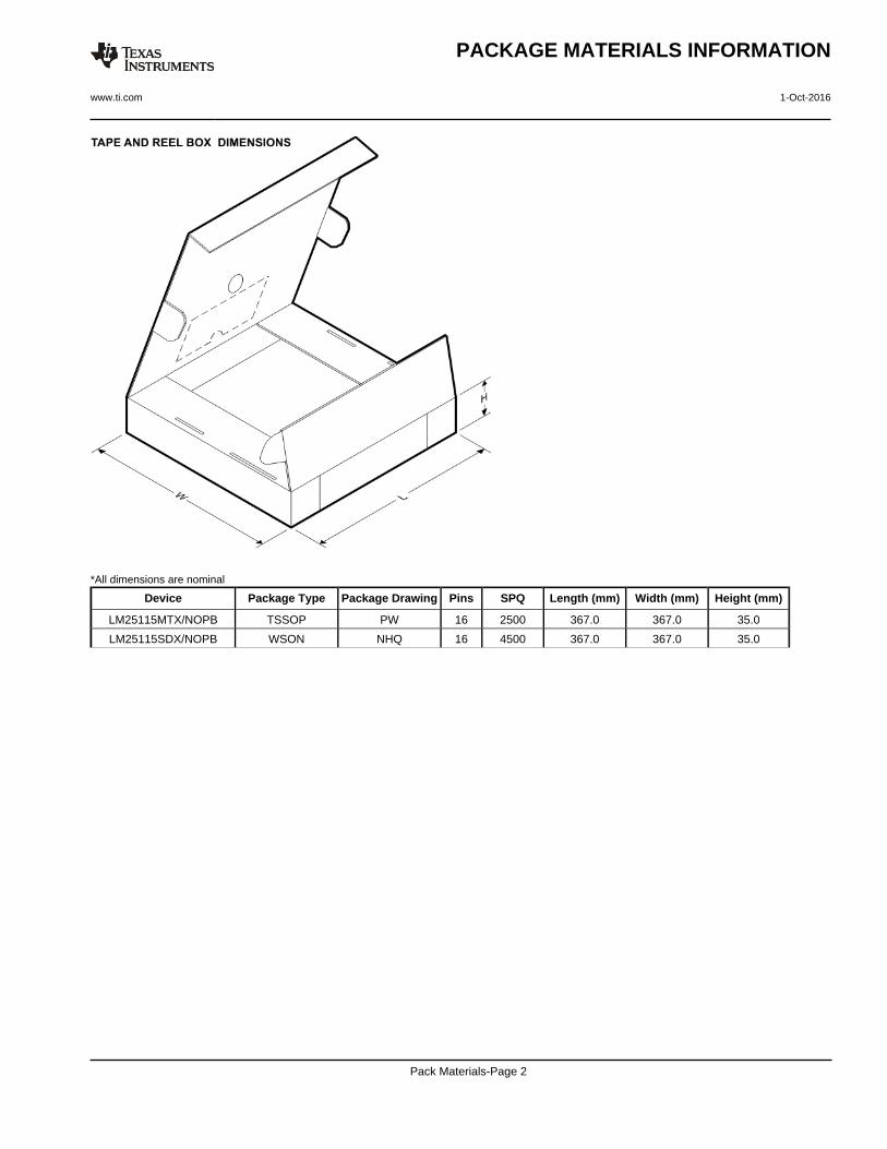
PACKAGE MATERIALS INFORMATION
www.ti.com 1-Oct-2016
Pack Materials-Page 1
*All dimensions are nominal
Device Package Type Package Drawing Pins SPQ Length (mm) Width (mm) Height (mm)
LM25115MTX/NOPB TSSOP PW 16 2500 367.0 367.0 35.0
LM25115SDX/NOPB WSON NHQ 16 4500 367.0 367.0 35.0
PACKAGE MATERIALS INFORMATION
www.ti.com 1-Oct-2016
Pack Materials-Page 2

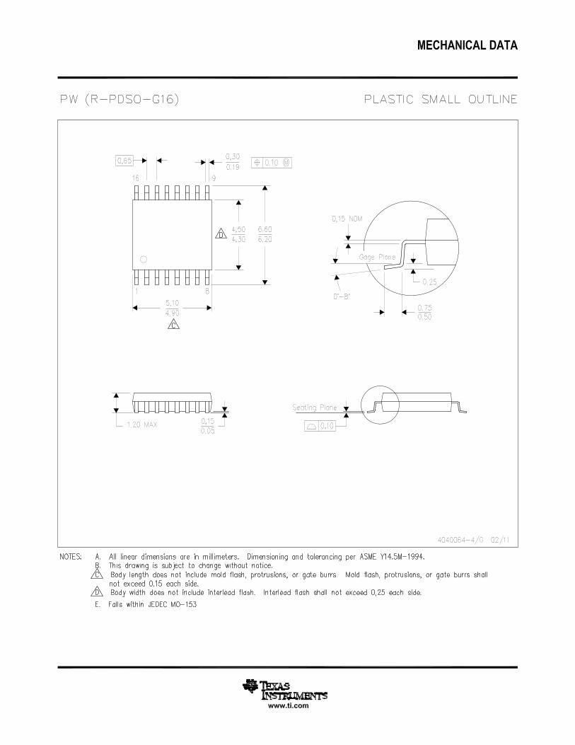
MECHANICAL DATA
NHQ0016A
www.ti.com
SDA16A (Rev A)

IMPORTANT NOTICE
Texas Instruments Incorporated and its subsidiaries (TI) reserve the right to make corrections, enhancements, improvements and otherchanges to its semiconductor products and services per JESD46, latest issue, and to discontinue any product or service per JESD48, latestissue. Buyers should obtain the latest relevant information before placing orders and should verify that such information is current andcomplete. All semiconductor products (also referred to herein as “components”) are sold subject to TI’s terms and conditions of salesupplied at the time of order acknowledgment.TI warrants performance of its components to the specifications applicable at the time of sale, in accordance with the warranty in TI’s termsand conditions of sale of semiconductor products. Testing and other quality control techniques are used to the extent TI deems necessaryto support this warranty. Except where mandated by applicable law, testing of all parameters of each component is not necessarilyperformed.TI assumes no liability for applications assistance or the design of Buyers’ products. Buyers are responsible for their products andapplications using TI components. To minimize the risks associated with Buyers’ products and applications, Buyers should provideadequate design and operating safeguards.TI does not warrant or represent that any license, either express or implied, is granted under any patent right, copyright, mask work right, orother intellectual property right relating to any combination, machine, or process in which TI components or services are used. Informationpublished by TI regarding third-party products or services does not constitute a license to use such products or services or a warranty orendorsement thereof. Use of such information may require a license from a third party under the patents or other intellectual property of thethird party, or a license from TI under the patents or other intellectual property of TI.Reproduction of significant portions of TI information in TI data books or data sheets is permissible only if reproduction is without alterationand is accompanied by all associated warranties, conditions, limitations, and notices. TI is not responsible or liable for such altereddocumentation. Information of third parties may be subject to additional restrictions.Resale of TI components or services with statements different from or beyond the parameters stated by TI for that component or servicevoids all express and any implied warranties for the associated TI component or service and is an unfair and deceptive business practice.TI is not responsible or liable for any such statements.Buyer acknowledges and agrees that it is solely responsible for compliance with all legal, regulatory and safety-related requirementsconcerning its products, and any use of TI components in its applications, notwithstanding any applications-related information or supportthat may be provided by TI. Buyer represents and agrees that it has all the necessary expertise to create and implement safeguards whichanticipate dangerous consequences of failures, monitor failures and their consequences, lessen the likelihood of failures that might causeharm and take appropriate remedial actions. Buyer will fully indemnify TI and its representatives against any damages arising out of the useof any TI components in safety-critical applications.In some cases, TI components may be promoted specifically to facilitate safety-related applications. With such components, TI’s goal is tohelp enable customers to design and create their own end-product solutions that meet applicable functional safety standards andrequirements. Nonetheless, such components are subject to these terms.No TI components are authorized for use in FDA Class III (or similar life-critical medical equipment) unless authorized officers of the partieshave executed a special agreement specifically governing such use.Only those TI components which TI has specifically designated as military grade or “enhanced plastic” are designed and intended for use inmilitary/aerospace applications or environments. Buyer acknowledges and agrees that any military or aerospace use of TI componentswhich have not been so designated is solely at the Buyer's risk, and that Buyer is solely responsible for compliance with all legal andregulatory requirements in connection with such use.TI has specifically designated certain components as meeting ISO/TS16949 requirements, mainly for automotive use. In any case of use ofnon-designated products, TI will not be responsible for any failure to meet ISO/TS16949.
Products ApplicationsAudio www.ti.com/audio Automotive and Transportation www.ti.com/automotiveAmplifiers amplifier.ti.com Communications and Telecom www.ti.com/communicationsData Converters dataconverter.ti.com Computers and Peripherals www.ti.com/computersDLP® Products www.dlp.com Consumer Electronics www.ti.com/consumer-appsDSP dsp.ti.com Energy and Lighting www.ti.com/energyClocks and Timers www.ti.com/clocks Industrial www.ti.com/industrialInterface interface.ti.com Medical www.ti.com/medicalLogic logic.ti.com Security www.ti.com/securityPower Mgmt power.ti.com Space, Avionics and Defense www.ti.com/space-avionics-defenseMicrocontrollers microcontroller.ti.com Video and Imaging www.ti.com/videoRFID www.ti-rfid.comOMAP Applications Processors www.ti.com/omap TI E2E Community e2e.ti.comWireless Connectivity www.ti.com/wirelessconnectivity
Mailing Address: Texas Instruments, Post Office Box 655303, Dallas, Texas 75265Copyright © 2016, Texas Instruments Incorporated