lmk04906 evaluation board user's guide (rev. a)
TRANSCRIPT

LMK04906 Evaluation Board
User's Guide
January 2012 Literature Number SNAU126A
Revised – December 2013

2 SNAU126A LMK04906 Family: Low-Noise Clock Jitter with Dual Loop PLLs Revised - December 2013 Copyright © 2013, Texas Instruments Incorporated
LMK04906 Family Low-Noise Clock Jitter Cleaner with Dual Loop PLLs
Evaluation Board Instructions
Revised - December 2013 LMK04906 Family: Low-Noise Clock Jitter with Dual Loop PLLs SNAU126A 3 Copyright © 2013, Texas Instruments Incorporated
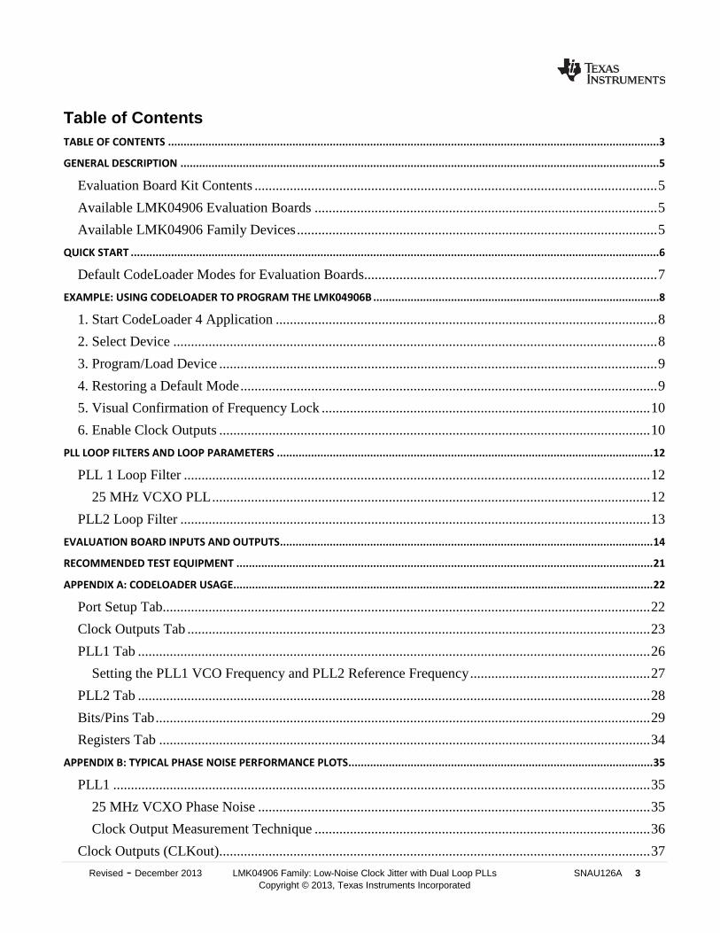
Table of Contents TABLE OF CONTENTS ..............................................................................................................................................................3
GENERAL DESCRIPTION ..........................................................................................................................................................5
Evaluation Board Kit Contents .................................................................................................................. 5
Available LMK04906 Evaluation Boards ................................................................................................. 5
Available LMK04906 Family Devices ...................................................................................................... 5
QUICK START ..........................................................................................................................................................................6
Default CodeLoader Modes for Evaluation Boards................................................................................... 7
EXAMPLE: USING CODELOADER TO PROGRAM THE LMK04906B ............................................................................................8
1. Start CodeLoader 4 Application ............................................................................................................ 8
2. Select Device ......................................................................................................................................... 8
3. Program/Load Device ............................................................................................................................ 9
4. Restoring a Default Mode ...................................................................................................................... 9
5. Visual Confirmation of Frequency Lock ............................................................................................. 10
6. Enable Clock Outputs .......................................................................................................................... 10
PLL LOOP FILTERS AND LOOP PARAMETERS ......................................................................................................................... 12
PLL 1 Loop Filter .................................................................................................................................... 12
25 MHz VCXO PLL ............................................................................................................................ 12
PLL2 Loop Filter ..................................................................................................................................... 13
EVALUATION BOARD INPUTS AND OUTPUTS ........................................................................................................................ 14
RECOMMENDED TEST EQUIPMENT ...................................................................................................................................... 21
APPENDIX A: CODELOADER USAGE....................................................................................................................................... 22
Port Setup Tab.......................................................................................................................................... 22
Clock Outputs Tab ................................................................................................................................... 23
PLL1 Tab ................................................................................................................................................. 26
Setting the PLL1 VCO Frequency and PLL2 Reference Frequency ................................................... 27
PLL2 Tab ................................................................................................................................................. 28
Bits/Pins Tab ............................................................................................................................................ 29
Registers Tab ........................................................................................................................................... 34
APPENDIX B: TYPICAL PHASE NOISE PERFORMANCE PLOTS .................................................................................................. 35
PLL1 ........................................................................................................................................................ 35
25 MHz VCXO Phase Noise ............................................................................................................... 35
Clock Output Measurement Technique ............................................................................................... 36
Clock Outputs (CLKout).......................................................................................................................... 37

4 SNAU126A LMK04906 Family: Low-Noise Clock Jitter with Dual Loop PLLs Revised - December 2013 Copyright © 2013, Texas Instruments Incorporated
LMK04906B CLKout Phase Noise ..................................................................................................... 37
APPENDIX C: SCHEMATICS .................................................................................................................................................... 38
Power Supplies......................................................................................................................................... 38
LMK04906B Device with Loop Filter and Crystal Circuits ................................................................... 39
Reference Inputs (CLKin0, CLKin1 & CLKin2), External VCXO (OSCin) & VCO Circuits............... 40
Clock Outputs (OSCout0, CLKout0 to CLKout5) .................................................................................. 41
uWire Header, Logic I/O Ports and Status LEDs .................................................................................... 42
APPENDIX D: BILL OF MATERIALS ......................................................................................................................................... 43
APPENDIX E: PCB LAYERS STACKUP ..................................................................................................................................... 47
APPENDIX F: PCB LAYOUT ..................................................................................................................................................... 48
Layer #1 – Top ......................................................................................................................................... 48
Layer #2 – RF Ground Plane (Inverted) .................................................................................................. 49
Layer #3 – Vcc Planes ............................................................................................................................. 50
Layer #4 – Ground Plane (Inverted) ........................................................................................................ 51
Layer # 5 – Vcc Planes 2 ......................................................................................................................... 52
Layer #6 – Bottom ................................................................................................................................... 53
Layers #1 and 6 – Top and Bottom (Composite) ..................................................................................... 54
APPENDIX G: PROPERLY CONFIGURING LPT PORT ................................................................................................................ 55
LPT Driver Loading ................................................................................................................................. 55
Correct LPT Port/Address........................................................................................................................ 55
Correct LPT Mode ................................................................................................................................... 56
Legacy Board Port Setup ......................................................................................................................... 56
APPENDIX H: TROUBLESHOOTING INFORMATION ................................................................................................................ 57
1) Confirm Communications ................................................................................................................ 57
2) Confirm PLL1 operation/locking ..................................................................................................... 57
3) Confirm PLL2 operation/locking ..................................................................................................... 58
APPENDIX I: EVM SOFTWARE AND COMMUNICATION ......................................................................................................... 59
OPTION 1 ................................................................................................................................................ 59
OPTION 2 ................................................................................................................................................ 59

Revised - December 2013 LMK04906 Family: Low-Noise Clock Jitter with Dual Loop PLLs SNAU126A 5 Copyright © 2013, Texas Instruments Incorporated
General Description The LMK04906 Evaluation Board simplifies evaluation of the LMK04906B Low-Noise Clock Jitter Cleaner with Dual Loop PLLs. Texas Instrument’s CodeLoader software can be used to program the internal registers of the LMK04906B device through the USB2ANY-uWIRE interface. The CodeLoader software will run on a Windows 2000/XP or Windows 7 PC and can be downloaded from http://www.ti.com/tool/codeloader. Evaluation Board Kit Contents The evaluation board kit includes:
• (1) LMK04906 Evaluation Board from Table 1 • (1) CodeLoader and USB2ANY-uWIRE Interface uWire header on EVM
Available LMK04906 Evaluation Boards The LMK04906 Evaluation Board supports any of the four devices offered in the LMK04906 Family. All evaluation boards use the same PCB layout and bill-of-materials, except for the corresponding LMK04906B device affixed to the board. A commercial-quality VCXO is also mounted to the board to provide a known reference point for evaluating device performance and functionality. Table 1: Available Evaluation Board Configurations
Evaluation Board ID Device PLL1 VCXO
LMK04906BEVAL LMK04906B 25 MHz Epson VCXO Model VG-4231CA 25.0000M-FGRC3
Available LMK04906 Family Devices Table 2: LMK04906B Devices
Device Reference Inputs
Buffered/ Divided OSCin
Outputs
Programmable LVDS/LVPECL/
LVCMOS Outputs
VCO Frequency
LMK04906B 3 1 6 2370 to 2600 MHz
6 SNAU126A LMK04906 Family: Low-Noise Clock Jitter with Dual Loop PLLs Revised - December 2013 Copyright © 2013, Texas Instruments Incorporated
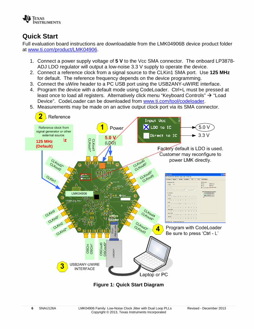
Quick Start Full evaluation board instructions are downloadable from the LMK04906B device product folder at www.ti.com/product/LMK04906.
1. Connect a power supply voltage of 5 V to the Vcc SMA connector. The onboard LP3878-ADJ LDO regulator will output a low-noise 3.3 V supply to operate the device.
2. Connect a reference clock from a signal source to the CLKin1 SMA port. Use 125 MHz for default. The reference frequency depends on the device programming.
3. Connect the uWire header to a PC USB port using the USB2ANY-uWIRE interface. 4. Program the device with a default mode using CodeLoader. Ctrl+L must be pressed at
least once to load all registers. Alternatively click menu “Keyboard Controls” “Load Device”. CodeLoader can be downloaded from www.ti.com/tool/codeloader.
5. Measurements may be made on an active output clock port via its SMA connector.
Figure 1: Quick Start Diagram
125 MHz (Default)

Revised - December 2013 LMK04906 Family: Low-Noise Clock Jitter with Dual Loop PLLs SNAU126A 7 Copyright © 2013, Texas Instruments Incorporated
Default CodeLoader Modes for Evaluation Boards CodeLoader saves the state of the selected LMK04906B device when exiting the software. To ensure a common starting point, the following modes listed in Table 3 may be restored by clicking “Mode” and selecting the appropriate device configuration, as shown in Figure 2 in the case of the LMK04906B device. Similar default modes are available for each LMK04906B device in CodeLoader. Choose a mode with CLKin0 or CLKin2 for differential clock signal or CLKin1 for a single ended signal.
Figure 2: Selecting a Default Mode for the LMK04906 Device After restoring a default mode, press Ctrl+L to program the device. The default modes also disable certain outputs, so make sure to enable the output under test to make measurements. Table 3: Default CodeLoader Modes for LMK04906
Default CodeLoader Mode Device Mode CLKin Frequency
OSCin Frequency
122.88 MHz CLKin1, 122.88 MHz VCXO Dual PLL, Internal VCO 122.88
MHz 122.88 MHz
125 MHz CLKin1, 25 MHz VCXO Dual PLL, Internal VCO 125 MHz 25 MHz The next section outlines step-by-step procedures for using the evaluation board with the LMK04906B. For boards with another part number, make sure to select the corresponding part number under the “Device” menu.

8 SNAU126A LMK04906 Family: Low-Noise Clock Jitter with Dual Loop PLLs Revised - December 2013 Copyright © 2013, Texas Instruments Incorporated
Example: Using CodeLoader to Program the LMK04906B The purpose of this section is to walk the user through using CodeLoader 4 to make some measurements with the LMK04906B device as an example. For more information on CodeLoader refer to Appendix A: CodeLoader Usage or the CodeLoader 4 instructions located at http://www.ti.com/tool/codeloader. Before proceeding, be sure to follow the Quick Start section above to ensure proper connections. 1. Start CodeLoader 4 Application Click “Start” “Programs” “CodeLoader 4” “CodeLoader 4” The CodeLoader 4 program is installed by default to the CodeLoader 4 application group. 2. Select Device Click “Select Device” “Clock Conditioners” “LMK04906B” Once started CodeLoader 4 will load the last used device. To load a new device, click “Select Device” from the menu bar. Then, select the subgroup and finally device to load. In this example, the LMK04906B is chosen. Selecting the device does cause the device to be programmed.
Figure 3 – Selecting the LMK04906B device

Revised - December 2013 LMK04906 Family: Low-Noise Clock Jitter with Dual Loop PLLs SNAU126A 9 Copyright © 2013, Texas Instruments Incorporated
3. Program/Load Device Assuming the Port Setup settings are correct, press the “Ctrl+L” shortcut or click “Keyboard Controls” “Load Device” from the menu to program the device to the current state of the newly loaded LMK04906 file. Once the device has been initially loaded, CodeLoader will automatically program changed registers so it is not necessary to re-load the device upon subsequent changes in the device configuration. It is possible to disable this functionality by ensuring there is no checkmark by the “Options” “AutoReload with Changes.” Because a default mode will be restored in the next step, this step is not really needed but is included to emphasize the importance of pressing “Ctrl+L” to load the device at least once after starting CodeLoader, restoring a mode, or restoring a saved setup using the File menu. See Appendix A: CodeLoader Usage or the CodeLoader 4 instructions located at http://www.ti.com/tool/codeloader for more information on Port Setup. Appendix H: Troubleshooting Information contains information on troubleshooting communications. 4. Restoring a Default Mode Click “Mode” “125 MHz CLKin1, 25 MHz VCXO”; then press Ctrl+L.
Figure 5: Setting the Default mode for LMK04906 For the purpose of this walkthrough, a default mode will be loaded to ensure a common starting point. This is important because when CodeLoader is closed, it remembers the last settings used for a particular device. Again, remember to press Ctrl+L as the first step after loading a default mode.
Figure 4 – Loading the Device
10 SNAU126A LMK04906 Family: Low-Noise Clock Jitter with Dual Loop PLLs Revised - December 2013 Copyright © 2013, Texas Instruments Incorporated
5. Visual Confirmation of Frequency Lock After a default mode is restored and loaded, LED D5 should illuminate when PLL1 and PLL2 are locked to the reference clock applied to CLKin1. This assumes LD_MUX = PLL1/2 DLD and LD_TYPE = Active High, which are the default settings. 6. Enable Clock Outputs While the LMK04906B offers programmable clock output buffer formats, the evaluation board is shipped with preconfigured output terminations to match the default buffer type for each output. Refer to the CLKout port description in the Evaluation Board Inputs and Outputs section. To measure phase noise at one of the clock outputs, for example, CLKout0:
1. Click on the Clock Outputs tab, 2. Uncheck “Powerdown” in the Digital Delay box to enable the channel, 3. Set the following settings as needed:
a. Digital Delay value b. Clock Divider value c. Analog Delay select and Analog Delay value (if not “Bypassed”) d. Clock Output type.
4. Depending on the configured output type, the clock output SMAs can be interfaced to a test
instrument with a single-ended 50-ohm input as follows. a. For LVDS:
i. A balun (like ADT2-1T) is recommended for differential-to-single-ended conversion.
b. For LVPECL: i. A balun can be used, or ii. One side of the LVPECL signal can be terminated with a 50-ohm load and the
other side can be run single-ended to the instrument. c. For LVCMOS:
i. There are two single-ended outputs, CLKoutX and CLKoutX*, and each output can be set to Normal, Inverted, or Off. There are nine (9) combinations of LVCMOS modes in the Clock Output list.
ii. One side of the LVCMOS signal can be terminated with a 50-ohm load and the other side can be run single-ended to the instrument.
iii. A balun may also be used. Ensure CLKoutX and CLKoutX* states are complementary to each other. That is, Norm/Inv or Inv/Norm.
Figure 7: Setting LVCMOS modes
Figure 6: Setting Digital Delay, Clock Divider, Analog Delay, and Output Format for CLKout0

Revised - December 2013 LMK04906 Family: Low-Noise Clock Jitter with Dual Loop PLLs SNAU126A 11 Copyright © 2013, Texas Instruments Incorporated
5. The phase noise may be measured with a spectrum analyzer or signal source analyzer. See Appendix B: Typical Phase Noise Performance Plots for phase noise plots of the clock outputs. National’s Clock Design Tool can be used to calculate divider values to achieve desired clock output frequencies. See: http://www.ti.com/tool/clockdesigntool.
12 SNAU126A LMK04906 Family: Low-Noise Clock Jitter with Dual Loop PLLs Revised - December 2013 Copyright © 2013, Texas Instruments Incorporated
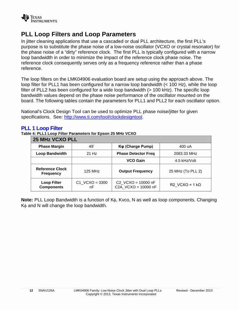
PLL Loop Filters and Loop Parameters In jitter cleaning applications that use a cascaded or dual PLL architecture, the first PLL’s purpose is to substitute the phase noise of a low-noise oscillator (VCXO or crystal resonator) for the phase noise of a “dirty” reference clock. The first PLL is typically configured with a narrow loop bandwidth in order to minimize the impact of the reference clock phase noise. The reference clock consequently serves only as a frequency reference rather than a phase reference. The loop filters on the LMK04906 evaluation board are setup using the approach above. The loop filter for PLL1 has been configured for a narrow loop bandwidth (< 100 Hz), while the loop filter of PLL2 has been configured for a wide loop bandwidth (> 100 kHz). The specific loop bandwidth values depend on the phase noise performance of the oscillator mounted on the board. The following tables contain the parameters for PLL1 and PLL2 for each oscillator option. National’s Clock Design Tool can be used to optimize PLL phase noise/jitter for given specifications. See: http://www.ti.com/tool/clockdesigntool. PLL 1 Loop Filter Table 4: PLL1 Loop Filter Parameters for Epson 25 MHz VCXO
25 MHz VCXO PLL Phase Margin 49˚ Kφ (Charge Pump) 400 uA
Loop Bandwidth 21 Hz Phase Detector Freq 2083.33 MHz
VCO Gain 4.5 kHz/Volt
Reference Clock Frequency 125 MHz Output Frequency 25 MHz (To PLL 2)
Loop Filter Components
C1_VCXO = 3300 nF
C2_VCXO = 10000 nF C2A_VCXO = 10000 nF R2_VCXO = 1 kΩ
Note: PLL Loop Bandwidth is a function of Kφ, Kvco, N as well as loop components. Changing Kφ and N will change the loop bandwidth.

Revised - December 2013 LMK04906 Family: Low-Noise Clock Jitter with Dual Loop PLLs SNAU126A 13 Copyright © 2013, Texas Instruments Incorporated
PLL2 Loop Filter Table 5: PLL2 Loop Filter Parameters for LMK04906B
LMK04906B C1_VCO 0.082 nF C2_VCO 5.6 nF
C3 (internal) 0.01 nF C4 (internal) 0.01 nF
R2_VCO 0.68 kΩ R3 (internal) 0.2 kΩ R4 (internal) 0.2 kΩ
Charge Pump Current, Kφ 3.2 mA
Phase Detector
Frequency 50 MHz
Frequency 2500 MHz Kvco 18.5 MHz/V
N 50
Phase Margin 69 degrees
Loop Bandwidth 132 kHz
Note: PLL Loop Bandwidth is a function of Kφ, Kvco, N as well as loop components. Changing Kφ and N will change the loop bandwidth.

14 SNAU126A LMK04906 Family: Low-Noise Clock Jitter with Dual Loop PLLs Revised - December 2013 Copyright © 2013, Texas Instruments Incorporated
Evaluation Board Inputs and Outputs The following table contains descriptions of the inputs and outputs for the evaluation board. Unless otherwise noted, the connectors described can be assumed to be populated by default. Additionally, some applicable CodeLoader programming controls are noted for convenience. Refer to the LMK04906 Family Datasheet for complete register programming information. Table 6: Evaluation Board Inputs and Outputs
Connector Name Signal Type, Input/Output Description
Populated: CLKout0, CLKout0*, CLKout1, CLKout1*, CLKout2, CLKout2*, CLKout3, CLKout3*, CLKout4, CLKout4*, CLKout5, CLKout5*
Analog, Output
Clock outputs with programmable output buffers. The output terminations by default on the evaluation board are shown below, and the output type selected by default in CodeLoader is indicated by an asterisk (*):
Clock output pair Default Board Termination CLKout0 LVPECL* CLKout1 LVPECL CLKout2 LVDS* / LVCMOS CLKout3 LVDS / LVCMOS CLKout4 LVDS* / LVCMOS CLKout5 LVPECL
Each CLKout pair has a programmable LVDS, LVPECL, or LVCMOS buffer. The output buffer type can be selected in CodeLoader in the Clock Outputs tab via the CLKoutX_TYPE control. All clock outputs are AC-coupled to allow safe testing with RF test equipment. All LVPECL clock outputs are source-terminated using 240-ohm resistors. If an output pair is programmed to LVCMOS, each output can be independently configured (normal, inverted, or off/tri-state).
Revised - December 2013 LMK04906 Family: Low-Noise Clock Jitter with Dual Loop PLLs SNAU126A 15 Copyright © 2013, Texas Instruments Incorporated
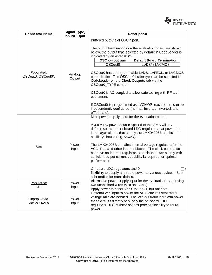
Connector Name Signal Type, Input/Output Description
Populated: OSCout0, OSCout0*,
Analog, Output
Buffered outputs of OSCin port. The output terminations on the evaluation board are shown below, the output type selected by default in CodeLoader is indicated by an asterisk (*):
OSC output pair Default Board Termination OSCout0 LVDS* / LVCMOS
OSCout0 has a programmable LVDS, LVPECL, or LVCMOS output buffer. The OSCout0 buffer type can be selected in CodeLoader on the Clock Outputs tab via the OSCout0_TYPE control. OSCout0 is AC-coupled to allow safe testing with RF test equipment. If OSCout0 is programmed as LVCMOS, each output can be independently configured (normal, inverted, inverted, and off/tri-state).
Vcc Power, Input
Main power supply input for the evaluation board. A 3.9 V DC power source applied to this SMA will, by default, source the onboard LDO regulators that power the inner layer planes that supply the LMK04906B and its auxiliary circuits (e.g. VCXO). The LMK04906B contains internal voltage regulators for the VCO, PLL and other internal blocks. The clock outputs do not have an internal regulator, so a clean power supply with sufficient output current capability is required for optimal performance. On-board LDO regulators and 0 r flexibility to supply and route power to various devices. See schematics for more details.
Populated: J1
Power, Input
Alternative power supply input for the evaluation board using two unshielded wires (Vcc and GND). Apply power to either Vcc SMA or J1, but not both.
Unpopulated: VccVCO/Aux
Power, Input
Optional Vcc input to power the VCO circuit if separated voltage rails are needed. The VccVCO/Aux input can power these circuits directly or supply the on-board LDO regulators. 0 Ω resistor options provide flexibility to route power.

16 SNAU126A LMK04906 Family: Low-Noise Clock Jitter with Dual Loop PLLs Revised - December 2013 Copyright © 2013, Texas Instruments Incorporated
Connector Name Signal Type, Input/Output Description
Populated: CLKin0, CLKin0*,
FBCLKin*/CLKin1* CLKin2, CLKin2*
Not Populated:
FBCLKin/CLKin1
Analog, Input
Reference Clock Inputs for PLL1 (CLKin0, 1, 2). CLKin1 can alternatively be used as an External Feedback Clock Input (FBCLKin) in 0-delay mode or an RF Input (Fin) in External VCO mode. Reference Clock Inputs for PLL1 (CLKin0, 1) FBCLKin/CLKin1* is configured by default for a single-ended reference clock input from a 50-ohm source. The non-driven input pin (FBCLKin/CLKin1) is connected to GND with a 0.1 uF. CLKin0/CLKin0* is configured by default for a differential reference clock input from a 50-ohm source. CLKin1* is the default reference clock input selected in CodeLoader. The clock input selection mode can be programmed on the Bits/Pins tab via the CLKin_Select_MODE control. Refer to the LMK04906 Family Datasheet section “Input Clock Switching” for more information. AC coupled Input Clock Swing Levels
Input Mode Min Max Units Differential Bipolar or
CMOS 0.5 3.1 Vpp
Single Ended
0.25 2.4 Vpp
External Feedback Input (FBCLKin) for 0-Delay CLKin1 is shared for use with FBCLKin as an external feedback clock input to PLL1 for 0-delay mode. See section, Error! Reference source not found. Error! Reference source not found., for more details on using 0-delay mode with the evaluation board and the evaluation board software. RF Input (Fin) for External VCO CLKin1 is also shared for use with Fin as an RF input for external VCO mode using the onboard VCO footprint (U3) or add-on VCO board. To enable Dual PLL mode with External VCO, the following registers must be properly configured in CodeLoader:
• MODE = (3) Dual PLL, Ext VCO (Fin), (5) Dual PLL, Ext VCO, 0-Delay, (11) PLL2, Ext VCO (Fin)

Revised - December 2013 LMK04906 Family: Low-Noise Clock Jitter with Dual Loop PLLs SNAU126A 17 Copyright © 2013, Texas Instruments Incorporated
Connector Name Signal Type, Input/Output Description
Not populated: OSCin, OSCin*
Analog, Input
Feedback VCXO clock input to PLL1 and Reference clock input to PLL2. By default, these SMAs are not connected to the traces going to the OSCin/OSCin* pins of the LMK04906B. Instead, the single-ended output of the onboard VCXO (U2) drives the OSCin* input of the device and the OSCin input of the device is connected to GND with 0.1 uF. A VCXO add-on board may be optionally attached via these SMA connectors with minor modification to the components going to the OSCin/OSCin* pins of device. This is useful if the VCXO footprint does not accommodate the desired VCXO device. A single-ended or differential signal may be used to drive the OSCin/OSCin* pins and must be AC coupled. If operated in single-ended mode, the unused input must be connected to GND with 0.1 uF. Refer to the LMK04906 Family Datasheet section “Electrical Characteristics” for PLL2 Reference Input (OSCin) specifications.
Test point: VTUNE1_TP
Analog, Output
Tuning voltage output from the loop filter for PLL1.
Test point: VTUNE2_TP
Analog, Output
Tuning voltage output from the loop filter for PLL2.
Populated: uWire
Test points:
DATAuWire_TP CLKuWIRE_TP LEuWIRE_TP
CMOS, Input/Output
10-pin header for uWire programming interface and programmable logic I/O pins for the LMK04906B. The uWire interface includes CLKuWire, DATAuWire, and LEuWire signals. The programmable logic I/O signals accessible through this header include: SYNC, Status_Holdover, Status_LD, Status_CLKin0, and Status_CLKin1. These logic I/O signals also have dedicated SMAs and test points.

18 SNAU126A LMK04906 Family: Low-Noise Clock Jitter with Dual Loop PLLs Revised - December 2013 Copyright © 2013, Texas Instruments Incorporated
Connector Name Signal Type, Input/Output Description
Test point: LD_TP
Not populated:
Status_LD
CMOS, Output
Programmable status output pin. By default, set to output the digital lock detect status signal for PLL1 and PLL2 combined. In the default CodeLoader modes, LED D5 will illuminate green when PLL lock is detected by the LMK04906B (output is high) and turn off when lock is lost (output is low). The status output signal for the Status_LD pin can be selected on the Bits/Pins tab via the LD_MUX control. Refer to the LMK04906 Family Datasheet section “Status Pins” and “Digital Lock Detect” for more information. Note: Before a high-frequency internal signal (e.g. PLL divider output signal) is selected by LD_MUX, it is suggested to first remove the 270 ohm resistor to prevent the LED from loading the output.
Test point: Holdover_TP
CMOS, Output
Programmable status output pin. By default, set to the output holdover mode status signal. In the default CodeLoader mode, LED D8 will illuminate red when holdover mode is active (output is high) and turn off when holdover mode is not active (output is low). Refer to the LMK04906 Family Datasheet section “Status Pins” and “Holdover Mode” for more information. Note: Before a high-frequency internal signal (e.g. PLL divider output signal) is selected by HOLDOVER_MUX, it is suggested to first remove the 270 ohm resistor to prevent the LED from loading the output.

Revised - December 2013 LMK04906 Family: Low-Noise Clock Jitter with Dual Loop PLLs SNAU126A 19 Copyright © 2013, Texas Instruments Incorporated
Connector Name Signal Type, Input/Output Description
Test point: CLKin0_SEL_TP CLKin1_SEL_TP
CMOS, Input/Output
Programmable status I/O pins. By default, set as input pins for controlling input clock switching of CLKin0 and CLKin1. These inputs will not be functional because CLKin_Select_MODE is set to 0 (CLKin0 Manual) by default in the Bits/Pins tab in CodeLoader. To enable input clock switching, CLKin_Select_MODE must be 3 or 6 and Status_CLKinX_TYPE must be 0 to 3 (pin enabled as an input). Input Clock Switching – Pin Select Mode When CLKin_SELECT_MODE is 3, the Status_CLKinX pins select which clock input is active as follows:
Status_CLKin1 Status_CLKin0 Active Clock 0 0 CLKin0 0 1 CLKin1 1 0 CLKin2 1 1 Holdover
Input Clock Switching – Auto with Pin Select When CLKin_SELECT_MODE is 6, the active clock is selected using the Status_CLKinX pins upon an input clock switch event as follows:
Status_CLKin1 Status_CLKin0 Active Clock
X 0 CLKin0 1 0 CLKin1 0 0 Reserved
Refer to the LMK04906 Family Datasheet section “Input Clock Switching” for more information. Status Outputs When Status_CLKinX_TYPE is 3 to 6 (pin enabled as an output), the status output signal for the corresponding Status_CLKinX pin can be programmed on the Bits/Pins tab via the Status_CLKinX_MUX control. Refer to the LMK04906 Family Datasheet section “Status Pins” for more information.

20 SNAU126A LMK04906 Family: Low-Noise Clock Jitter with Dual Loop PLLs Revised - December 2013 Copyright © 2013, Texas Instruments Incorporated
Connector Name Signal Type, Input/Output Description
Test point: SYNC_TP
CMOS, Input/Output
Programmable status I/O pin. By default, set as an input pin for synchronize the clock outputs with a fixed and known phase relationship between each clock output selected for SYNC. A SYNC event also causes the digital delay values to take effect. In the default CodeLoader mode, SYNC will asserted when the SYNC pin is low and the outputs to be synchronized will be held in a logic low state. When SYNC is unasserted, the clock outputs to be synchronized are activated and will be initially phase aligned with each other except for outputs programmed with different digital delay values. A SYNC event can also be programmed by toggling the SYNC_POL_INV bit in the Bits/Pins tab in CodeLoader. Refer to the LMK04906 Family Datasheet section “Clock Output Synchronization” for more information. Status Output When SYNC_MUX is 3 to 6 (pin enabled as output), a status signal for the SYNC pin can be selected on the Bits/Pins tab via the SYNC_MUX control.

Revised - December 2013 LMK04906 Family: Low-Noise Clock Jitter with Dual Loop PLLs SNAU126A 21 Copyright © 2013, Texas Instruments Incorporated
Recommended Test Equipment Power Supply The Power Supply should be a low noise power supply, particularly when the devices on the board are being directly powered (onboard LDO regulators bypassed). Phase Noise / Spectrum Analyzer To measure phase noise and RMS jitter, an Agilent E5052 Signal Source Analyzer is recommended. An Agilent E4445A PSA Spectrum Analyzer with the Phase Noise option is also usable although the architecture of the E5052 is superior for phase noise measurements. At frequencies less than 100 MHz the local oscillator noise of the E4445A is too high and measurements will reflect the E4445A’s internal local oscillator performance, not the device under test. Oscilloscope To measure the output clocks for AC performance, such as rise time or fall time, propagation delay, or skew, it is suggested to use a real-time oscilloscope with at least 1 GHz analog input bandwidth (2.5+ GHz recommended) with 50 ohm inputs and 10+ Gsps sample rate. To evaluate clock synchronization or phase alignment between multiple clock outputs, it’s recommended to use phase-matched, 50-ohm cables to minimize external sources of skew or other errors/distortion that may be introduced if using oscilloscope probes.
22 SNAU126A LMK04906 Family: Low-Noise Clock Jitter with Dual Loop PLLs Revised - December 2013 Copyright © 2013, Texas Instruments Incorporated
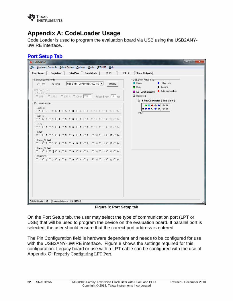
Appendix A: CodeLoader Usage Code Loader is used to program the evaluation board via USB using the USB2ANY-uWIRE interface. . Port Setup Tab
Figure 8: Port Setup tab
On the Port Setup tab, the user may select the type of communication port (LPT or USB) that will be used to program the device on the evaluation board. If parallel port is selected, the user should ensure that the correct port address is entered. The Pin Configuration field is hardware dependent and needs to be configured for use with the USB2ANY-uWIRE interface. Figure 8 shows the settings required for this configuration. Legacy board or use with a LPT cable can be configured with the use of Appendix G: Properly Configuring LPT Port.

Revised - December 2013 LMK04906 Family: Low-Noise Clock Jitter with Dual Loop PLLs SNAU126A 23 Copyright © 2013, Texas Instruments Incorporated
Clock Outputs Tab
Figure 9: Clock Outputs Tab
The Clock Outputs tab allows the user to control the output channel blocks, including:
• Clock Group Source from either VCO or OSCin (via OSC Mux1 and OSC Mux2) • Channel Powerdown (affects digital and analog delay, clock divider, and buffer
blocks) • Digital Delay value and Half Step • Clock Divide value • Analog Delay value and Delay bypass/enable (per output) • Clock Output format (per output)

24 SNAU126A LMK04906 Family: Low-Noise Clock Jitter with Dual Loop PLLs Revised - December 2013 Copyright © 2013, Texas Instruments Incorporated
This tab also allows the user to select the VCO Divider value (2 to 8). Note that the total PLL2 N divider value is the product of the VCO Divider value and the PLL N Prescaler and N Counter values (shown in the PLL2 tab), and is given by:
PLL2 N Total = VCO Divider * PLL2 N Prescaler * PLL2 N Counter Clicking on the cyan-colored PLL2 block that contains R, PDF and N values will bring the PLL2 tab into focus where these values may be modified, if needed. Clicking on the values in the box containing the Internal Loop Filter component (R3, C3, R4, C4) allow one to step through the possible values. Left click to increase the component value, and right click to decrease the value. These values can also be changed in the Bits/Pins tab. The Reference Oscillator value field may be changed in either the Clock Outputs tab or the PLL2 tab. The PLL2 Reference frequency should match the frequency of the onboard VCXO or Crystal (i.e., VCO frequency in the PLL1 tab); if not, a warning message will appear to indicate that the PLL(s) may be out of lock, as highlighted by the red box in Figure 10.

Revised - December 2013 LMK04906 Family: Low-Noise Clock Jitter with Dual Loop PLLs SNAU126A 25 Copyright © 2013, Texas Instruments Incorporated
Figure 10: Warning message indicating mismatch between
26 SNAU126A LMK04906 Family: Low-Noise Clock Jitter with Dual Loop PLLs Revised - December 2013 Copyright © 2013, Texas Instruments Incorporated
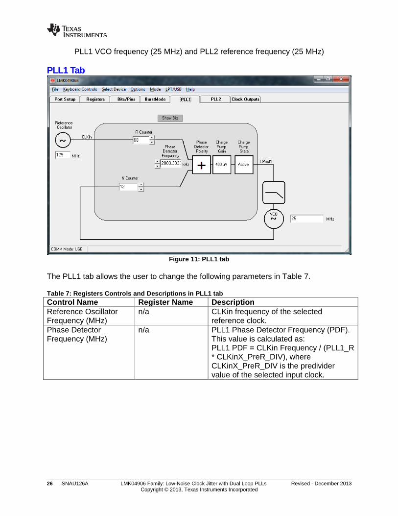
PLL1 VCO frequency (25 MHz) and PLL2 reference frequency (25 MHz) PLL1 Tab
Figure 11: PLL1 tab
The PLL1 tab allows the user to change the following parameters in Table 7. Table 7: Registers Controls and Descriptions in PLL1 tab Control Name Register Name Description Reference Oscillator Frequency (MHz)
n/a CLKin frequency of the selected reference clock.
Phase Detector Frequency (MHz)
n/a PLL1 Phase Detector Frequency (PDF). This value is calculated as: PLL1 PDF = CLKin Frequency / (PLL1_R * CLKinX_PreR_DIV), where CLKinX_PreR_DIV is the predivider value of the selected input clock.
Revised - December 2013 LMK04906 Family: Low-Noise Clock Jitter with Dual Loop PLLs SNAU126A 27 Copyright © 2013, Texas Instruments Incorporated
VCO Frequency (MHz) n/a The VCO Frequency should be the OSCin frequency, except when operating in Dual PLL with 0-delay feedback. This value is calculated as: VCO Freq (OSCin freq) = PLL1 PDF * PLL1_N. In Dual PLL mode with 0-delay feedback, the VCO frequency should be set to the feedback clock input frequency. See the section Setting the PLL1 VCO Frequency and PLL2 Reference Frequency for details.
R Counter PLL1_R PLL1 R Counter value (1 to 16383). N Counter PLL1_N PLL1 N Counter value (1 to 16383). Phase Detector Polarity PLL1_CP_POL PLL1 Phase Detector Polarity.
Click on the polarity sign to toggle polarity “+” or “–”.
Charge Pump Gain PLL1_CP_GAIN PLL1 Charge Pump Gain. Left-click/right-click to increase/decrease charge pump gain (100, 200, 400, 1600 uA).
Charge Pump State PLL1_CP_TRI PLL1 Charge Pump State. Click to toggle between Active and Tri-State.
Setting the PLL1 VCO Frequency and PLL2 Reference Frequency When operating in Dual PLL mode without 0-delay feedback, the VCO frequency value on the PLL1 tab must match the Reference Oscillator (OSCin) frequency value on the PLL2 tab; otherwise, the one or both PLLs may be out of lock. Updating the Reference Oscillator frequency on the PLL2 tab will automatically update the value of OSCin_FREQ on the Bits/Pins tab.
28 SNAU126A LMK04906 Family: Low-Noise Clock Jitter with Dual Loop PLLs Revised - December 2013 Copyright © 2013, Texas Instruments Incorporated
PLL2 Tab
Figure 12: PLL2 tab
The PLL2 tab allows the user to change the following parameters in Table 8. Table 8: Registers Controls and Descriptions in PLL2 tab Control Name Register Name Description Reference Oscillator Frequency (MHz)
OSCin_FREQ OSCin frequency from the External VCXO or Crystal.
Phase Detector Frequency (MHz)
n/s PLL2 Phase Detector Frequency (PDF). This value is calculated as: PLL2 PDF = OSCin Frequency *(2EN_PLL2_REF_2X) / PLL2_R.
VCO Frequency (MHz) n/a Internal VCO Frequency should be within the allowable range of the LMK04906B device. This value is calculated as: VCO Frequency = PLL2 PDF * (PLL2_N * PLL2_P * VCO divider value).
Doubler EN_PLL2_REF_2X PLL2 Doubler. 0 = Bypass Doubler 1 = Enable Doubler
R Counter PLL2_R PLL2 R Counter value (1 to 4095). N Counter PLL2_N PLL2 N Counter value (1 to 262143). PLLN Prescaler PLL2_P PLL2 N Prescaler value (2 to 8).

Revised - December 2013 LMK04906 Family: Low-Noise Clock Jitter with Dual Loop PLLs SNAU126A 29 Copyright © 2013, Texas Instruments Incorporated
Phase Detector Polarity PLL2_CP_POL PLL2 Phase Detector Polarity. Click on the polarity sign to toggle polarity “+” or “–”.
Charge Pump Gain PLL2_CP_GAIN PLL2 Charge Pump Gain. Left-click/right-click to increase/decrease charge pump gain (100, 400, 1600, 3200 uA).
Charge Pump State PLL2_CP_TRI PLL2 Charge Pump State. Click to toggle between Active and Tri-State.
Changes made on this tab will be reflected in the Clock Outputs tab. The VCO Frequency should conform to the specified internal VCO frequency range for the LMK04906B device (per Table 2). Bits/Pins Tab
Figure 13: Bits/Pins tab
The Bits/Pins tab allows the user to program bits directly, many of which are not available on other tabs. Brief descriptions for the controls on this tab are provided in Table 9 to supplement the datasheet. Refer to the LMK04906 Family Datasheet for more information.
30 SNAU126A LMK04906 Family: Low-Noise Clock Jitter with Dual Loop PLLs Revised - December 2013 Copyright © 2013, Texas Instruments Incorporated
TIP: Right-clicking any register name in the Bits/Pins tab will display a Help prompt with the register address, data bit location/length, and a brief register description. Table 9: Register Controls and Descriptions on Bits/Pins tab Group Register Name Description
Mod
e C
ontro
l
RESET Resets the device to default register values. RESET must be cleared for normal operation to prevent an unintended reset every time R0 is programmed.
POWERDOWN Places the device in powerdown mode. MODE Selects the operating mode (topology) for the
LMK04906 device. PD_OSCin Powers down the OSCin buffer. For use in Clock
Distribution mode if OSCin path is not used. FEEDBACK_MUX Selects the feedback source for 0-delay mode. OSCin_FREQ Must be set to the OSCin frequency range for
PLL2. Used for proper operation of the internal VCO calibration routine. Entering a reference oscillator frequency on PLL2 tab will automatically update OSCin_FREQ to the proper frequency range.
VCO_MUX Selects between VCO and VCO divider to drive the clock distribution path. The VCO divider is only valid if MODE is selecting the Internal VCO.
uWire_LOCK When checked, no other uWire programming will have effect. Must be unchecked to enable uWire programming of registers R0 to R30.
CLK
in
CLKin_Select_MODE Selects operational mode for how the device selects the reference clock for PLL1.
EN_CLKin1 Enables CLKin1 as a usable reference input during auto switching mode.
EN_CLKin0 Enables CLKin0 as a usable reference input during auto switching mode.
CLKinX_BUF_TYPE Selects the CLKinX input buffer to Bipolar (internal 0 mV offset) or MOS (internal 55 mV offset).
EN_LOS Enable the Loss-Of-Signal (LOS) detect circuitry.
LOS_TIMEOUT Sets the timeout value for the LOS detect circuitry to assert a loss of signal state on a clock input.
Crystal EN_PLL2_XTAL Enables Crystal Oscillator XTAL_LVL Sets peak amplitude on the tunable crystal.
Values listed are for a 20.48 MHz crystal.
IO C
ontro
l LD_MUX Sets the selected signal on the Status_LD pin. LD_TYPE Sets I/O pin type on the Status_LD pin. HOLDOVER_MUX Sets the selected signal on the
Status_HOLDOVER pin. HOLDOVER_TYPE Sets I/O pin type on the Status_Holdover pin.
Revised - December 2013 LMK04906 Family: Low-Noise Clock Jitter with Dual Loop PLLs SNAU126A 31 Copyright © 2013, Texas Instruments Incorporated
Status_CLKin0 _MUX Sets the selected signal on the Status_CLKin0 pin.
Status_CLKin0_TYPE Sets I/O pin type on the Status_CLKin0 pin. Status_CLKin1_MUX Sets the selected signal on the Status_CLKin1
pin. Status_CLKin1_TYPE Sets I/O pin type on the Status_CLKin1 pin. CLKin_Sel_INV Inverts the Status_CLKin0/1 pin polarity when
set to an input type. Significant when CLKin_SELECT_MODE is 3 or 6.
IO C
ontro
l – S
ync
SYNC_MUX Sets the selected signal on the SYNC pin. SYNC_TYPE Sets I/O pin type on the SYNC pin. SYNC_POL_INV Sets polarity on SYNC input to active low
when checked. Toggling this bit will initiate a SYNC event.
SYNC_PLL1_DLD Engage SYNC mode until PLL1 DLD is true SYNC_PLL2_DLD Engage SYNC mode until PLL2 DLD is true NO_SYNC_CLKoutX_Y Synchronization will not affect selected clock
outputs, where X = even-numbered output and Y = odd-numbered output.
SYNC_QUAL Sets the SYNC to qualify mode for dynamic digital delay.
EN_SYNC Must be set when using SYNC, but may be cleared after the SYNC event. When using dynamic digital delay (SYNC_QUAL = 1), EN_SYNC must always be set. Changing this value from 0 to 1 can cause a SYNC event, so clocks which should not be SYNCed when setting this bit should have the NO_SYNC_CLKoutX_Y bit set. NOTE: This bit is not a valid method of generating a SYNC event. Use one of the other SYNC generation methods to ensure a proper SYNC occurs.
SYNC_EN_AUTO Enable auto SYNC when R0 to R5 is written.
DA
C/H
oldo
ver
HOLDOVER_MODE Sets holdover mode to be disabled or enabled. FORCE_HOLDOVER Engages holdover when checked regardless of
HOLDOVER_MODE value. Turns the DAC on.
EN_TRACK Enables DAC tracking. DAC tracks the PLL1 Vtune to provide for an accurate HOLDOVER mode. DAC_CLK_DIV should also be set so that DAC update rate is <= 100 kHz.
32 SNAU126A LMK04906 Family: Low-Noise Clock Jitter with Dual Loop PLLs Revised - December 2013 Copyright © 2013, Texas Instruments Incorporated
EN_VTUNE_RAIL_DET Allows rail-to-rail operation of VCXO with default of 0. Allows use of DAC_LOW_TRIP, DAC_HIGH_TRIP. Must be used with EN_MAC_DAC = 1. CLKin_SELECT_MODE must be 4 or 6 (auto mode) to use.
HOLD_DLD_CNT In HOLDOVER mode, wait for this many clocks of PLL1 PDF within the tolerances of PLL1_WND _SIZE before exiting holdover mode.
DAC_CLK_DIV DAC update clock is the PLL1 phase detector divided by this divisor. For proper operation, DAC update clock rate should be <= 100 kHz. DAC update rate = PLL1 phase detector frequency / DAC_CLK_DIV
EN_MAN_DAC Enables manual DAC mode and set DAC voltage when in holdover.
MAN_DAC Sets the value for the DAC when EN_MAN_DAC is 1 and holdover is engaged. Readback from this register is the current DAC value whether in manual DAC mode or DAC tracking mode
DAC_LOW_TRIP Value from GND in ~50mV steps at which a clock switch event is generated. If Holdover mode is enabled, it will be engaged upon the clock switch event. NOTE: EN_VTUNE_RAIL_DET must be enabled for this to be valid.
DAC_HIGH_TRIP Value from VCC (3.3V) in ~50mV steps at which clock switch event is generated. If Holdover mode is enabled, it will be engaged upon the clock switch event. NOTE: EN_VTUNE_RAIL_DET must be enabled for this to be valid.
PLL
1
PLL1_WND_SIZE If the phase error between the PLL1 reference and feedback clocks is less than specified time, then the PLL1 lock counter increments. NOTE: Final lock detect valid signal is determined when the PLL1 lock counter meets or exceeds the PLL1_DLD_CNT value.
PLL1_DLD_CNT The reference and feedback of PLL1 must be within the window of phase error as specified by PLL1_WND_SIZE for this many cycles before PLL1 digital lock detect is asserted.
CLKinX_PreR_DIV The PreR dividers divide the CLKinX reference before the PLL1_R divider. Unique divides on individual CLKinX signals allows switchover from one clock input to another clock input without needing to reprogram the PLL1_R divider to keep the device in lock.

Revised - December 2013 LMK04906 Family: Low-Noise Clock Jitter with Dual Loop PLLs SNAU126A 33 Copyright © 2013, Texas Instruments Incorporated
PLL1_N_DLY N delay causes clock outputs to lead clock input when in a 0-delay mode. Increasing the N delay value increases the output phase lead relative to the input.
PLL1_R_DLY R delay causes clock outputs to lag clock input when in a 0-delay mode. Increasing the R delay value increases the output phase lag relative to the input.
PLL2
PLL2_WND_SIZE If the phase error between the PLL2 reference and feedback clock is less than specified time, then the PLL2 lock counter increments.
PLL2_DLD_CNT The reference and feedback of PLL2 must be within the window of phase error as specified by PLL2_WND_SIZE for this many cycles before PLL2 digital lock detect is asserted.
EN_PLL2_REF_2X Enables the doubler block to doubles the reference frequency into the PLL2 R counter. This can allow for frequency of 2/3, 2/5, etc. of OSCin to be used at the phase detector of PLL2.
PLL2_N_CAL The PLL2_N_CAL register contains the N value used for the VCO calibration routine. Except during 0-delay modes, the PLL2_N and PLL2_N_CAL registers will be exactly the same.
PLL2_R3_LF Set the corresponding integrated PLL2 loop filter values: R3, R4, C3, and C4. It is also possible to set these values by clicking on the loop filter values on the Clock Outputs tab.
PLL2_R4_LF PLL2_C3_LF PLL2_C4_LF PLL2_FAST_PDF Enable this bit when using a PLL2 phase detector
frequency > 100 MHz.
Program Pins SYNC Sets these pins on the uWire header to logic high
(checked) or logic low (unchecked). Status_CLKin0 Status_CLKin1
34 SNAU126A LMK04906 Family: Low-Noise Clock Jitter with Dual Loop PLLs Revised - December 2013 Copyright © 2013, Texas Instruments Incorporated
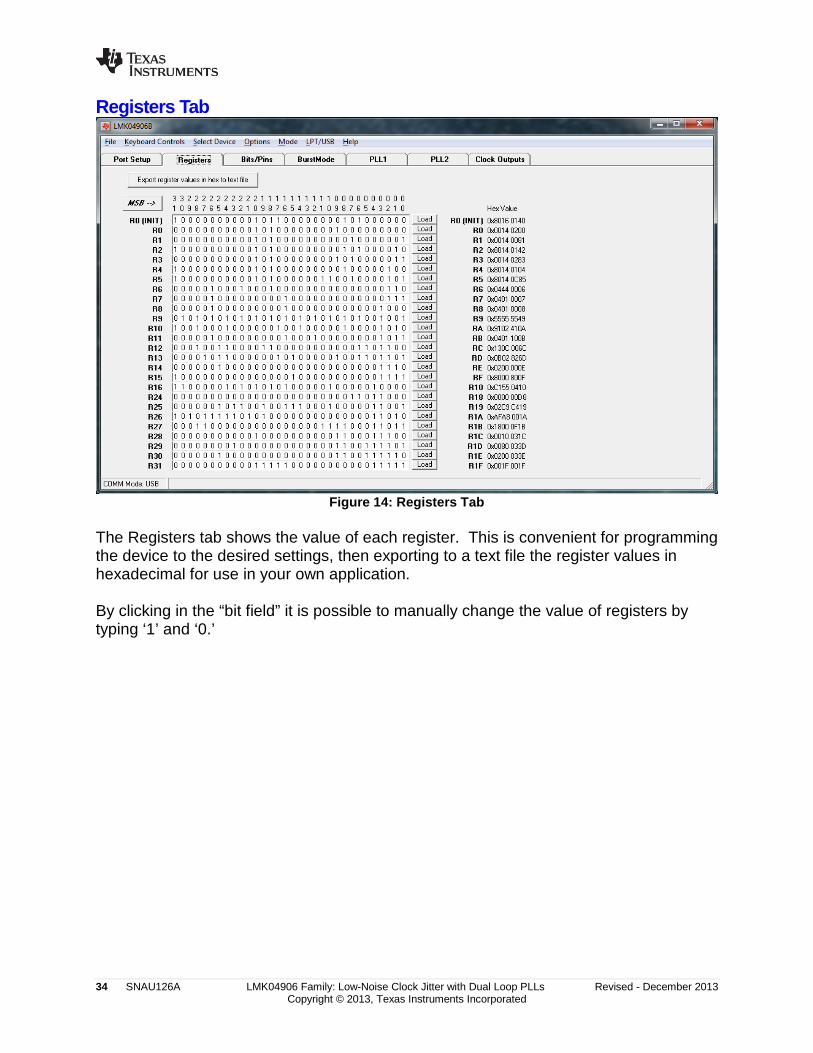
Registers Tab
Figure 14: Registers Tab
The Registers tab shows the value of each register. This is convenient for programming the device to the desired settings, then exporting to a text file the register values in hexadecimal for use in your own application. By clicking in the “bit field” it is possible to manually change the value of registers by typing ‘1’ and ‘0.’
Revised - December 2013 LMK04906 Family: Low-Noise Clock Jitter with Dual Loop PLLs SNAU126A 35 Copyright © 2013, Texas Instruments Incorporated
Appendix B: Typical Phase Noise Performance Plots PLL1 The LMK04906B’s dual PLL architecture achieves ultra low jitter and phase noise by allowing the external VCXO or Crystal’s phase noise to dominate the final output phase noise at low offset frequencies and the internal VCO’s phase noise to dominate the final output phase noise at high offset frequencies. This results in the best overall noise and jitter performance. Table 10 lists the test conditions used for output clock phase noise measurements with the Epson 25 MHz VCXO. Table 10: LMK04906B Test Conditions Parameter Value PLL1 Reference clock input CLKin1 single-ended input, CLKin1* AC-coupled to
GND PLL1 Reference Clock frequency
125 MHz
PLL1 Phase detector frequency 2083.33 MHz PLL1 Charge Pump Gain 400 uA VCXO frequency 25 MHz PLL2 phase detector frequency 50 MHz PLL2 Charge Pump Gain 3200 uA PLL2 REF2X mode Disabled
25 MHz VCXO Phase Noise The phase noise of the reference is masked by the phase noise of this VCXO by using a narrow loop bandwidth for PLL1 while retaining the frequency accuracy of the reference clock input. This VCXO sets the reference noise to PLL2. Figure 15 shows the open loop typical phase noise performance of the Epson VG-4231CA 25.0000M-FGRC3 VCXO.

36 SNAU126A LMK04906 Family: Low-Noise Clock Jitter with Dual Loop PLLs Revised - December 2013 Copyright © 2013, Texas Instruments Incorporated
Figure 15: Epson VG-4231CA 25 MHz VCXO Phase Noise at 25 MHz
Table 11: VCXO Phase Noise at 25 MHz (dBc/Hz)
Offset Phase Noise
10 Hz -73.6 100 Hz -103.7
1 kHz -130.8 10 kHz -147.6
100 kHz -155.42 1 MHz -160.4
10 MHz -168.1 40 MHz -168.1
Table 12: VCXO RMS Jitter to high offset of 20 MHz
at 25 MHz (rms fs) Low
Offset Jitter
10 Hz 515.4 100 Hz 60.5
1 kHz 36.2 10 kHz 35.0
100 kHz 34.5 1 MHz 32.9
10 MHz 22.7
Clock Output Measurement Technique The same technique was used to measure phase noise for all three output types available on the programmable OSCout and CLKout buffers. This was achieved by connection the differential outputs to a Prodyn GXXX Balun and measuring the side single-ended using an Agilent E5052B Source Signal Analyzer.
-170-160-150-140-130-120-110-100
-90-80-70-60-50
10 100 1000 10000 100000 1000000 10000000
Phas
e N
oise
(dB
c/H
z)
Offset (Hz)
VCXO Phase Noise
CVHD-930-25

Revised - December 2013 LMK04906 Family: Low-Noise Clock Jitter with Dual Loop PLLs SNAU126A 37 Copyright © 2013, Texas Instruments Incorporated
Clock Outputs (CLKout) The LMK04906 Family features programmable LVDS, LVPECL, and LVCMOS buffer modes for the CLKoutX and OSCout0 output pairs. Included below are various phase noise measurements for each output format. For the LMK04906B, the internal VCO frequency is 2500 MHz. The divide-by-4 CLKout frequency is 625 MHz, the divide-by-16 CLKout frequency is 156.25 MHz, and the divide-by-20 CLKout frequency is 125 MHz.
LMK04906B CLKout Phase Noise
Figure 16: LMK04906B CLKout Phase Noise
Table 13: LMK04906B Phase Noise (dBc/Hz) Phase Noise and RMS Jitter (fs)
Offset 625 MHz LVPECL 1.6
156.25 MHz LVPECL 1.6
125 MHz LVPECL 1.6
100 Hz -76.0 -88.0 -90.8 1 kHz -103.2 -115.6 -117.1
10 kHz -118.1 -130.2 -132.2 100 kHz -121.5 -134.0 -136.0
800 kHz -140.5 -152.5 -154.3 1 MHz -142.7 -154.4 -156.1
10 MHz -154.6 -161.1 -161.7 20 MHz -154.8 -161.1 -161.8
RMS Jitter (fs) 12 kHz to 20 MHz 146.0 147.4 149.5
RMS Jitter (fs) 1 kHz to 5 MHz 166.4 160.6 159.8
-170
-160
-150
-140
-130
-120
-110
-100
-90
-80
-70
100 1000 10000 100000 1000000 10000000
Phas
e N
oise
(dBc
/Hz)
Frequency Offset (Hz)
LMK04906B CLKout Phase Noise
156.25 MHz LVPECL16
125 MHz LVPECL16
625 MHz LVPECL16

38 SNAU126A LMK04906 Family: Low-Noise Clock Jitter with Dual Loop PLLs Revised - December 2013 Copyright © 2013, Texas Instruments Incorporated
Appendix C: Schematics Power Supplies

Revised - December 2013 LMK04906 Family: Low-Noise Clock Jitter with Dual Loop PLLs SNAU126A 39 Copyright © 2013, Texas Instruments Incorporated
LMK04906B Device with Loop Filter and Crystal Circuits
1
1
2
2
3
3
4
4
5
5
6
6
D D
C C
B B
A A
3 8Main Sheet / IC
8/1/2013
LMK049xx_PLL.SchDoc
Sheet Title:Size: Schematic:
Mod. Date:
File:
Rev:Sheet: of
B
Texas Instruments and/or its licensors do not warrant the accuracy or completeness of thisspecification or any information contained therein. Texas Instruments and/or its licensors do notwarrant that this design will meet the specifications, will be suitable for your application or fit forany particular purpose, or will operate in an implementation. Texas Instruments and/or itslicensors do not warrant that the design is production worthy. You should completely validateand test your design implementation to confirm the system functionality for your application. http://www.ti.com
Contact: http://www.national.com/support
LMK049xx Evaluation BoardProject:Designed for:Evaluation Customer
870600738 1Assembly Variant: 12-21-2011
© Texas Instruments CopyrightYear
100pFC2p_VCODNP
0.1µF
C38DNP
0.1µF
C30
10uFC2_VCXO
0R40DNP
2pF
C36DNP
2200pF
C34DNP
2pF
C31DNP
2200pF
C32DNP
PLL2 Loop Filter
PLL1 Loop Filter
OSCin Tuneable Crystal4.7k
R36DNP
1000pFC33DNP
10k
R38DNP
VCXO Loop Filter
Y300DNP
DNP
VTUNE2_TP
0
R42
Designators greater than and equal to 200 are placed on bottom of PCB
10µFC37
0.1µFC39
CLKout0_P
CLKout0_N
CLKout1_P
CLKout1_N
CLK
out2
_P
CLK
out2
_N
CLK
in0_
P
CLK
in0_
N
CLK
in1_
P
CLK
in1_
N
CLK
in2_
P
CLK
in2_
N
Stat
us_H
old
Status_LD
Sta
tus_
CLK
in0
Sta
tus_
CLK
in1
CLK
out5
_N
CLK
out5
_P
CLK
out4
_N
CLK
out4
_P
CLK
out3
_N
CLK
out3
_P
SYNC
0R35DNPuWire_DATA
uWire_CLK
uWire_LE
OSCout0_N
OSCout0_PVcc1_VCO
Vcc2_CLKout_CG1
Vcc3_CLKout_CG2 Vcc4_Digital Vcc5_CLKin
Vcc6_PDCP1
Vcc7_OSC
Vcc9_PLL2
Vcc12_CLKout_CG5
Vcc13_CLKout_CG0
Vcc8_PDCP2
OSCin_N
OSCin_P
4.7k
R39DNP
VTUNE1_TP
Vtune_VCXO
Status_Hold
SYNC
Status_LD
Status_CLKin0
Status_CLKin1
uWire_LE
uWire_DATA
uWire_CLK
0.1µFC35DNP
0
R43
VCO_Vtune0
R34DNP
0.1µFC40
3.3µFC1_VCXO
10uFC2A_VCXO
1kR2_VCXO
620R2_VCO
47pFC1_VCO 3900pF
C2_VCO
OSCin_1_N
OSCin_1_P
1
3
2
SMV1249-074LFD1
DNP
CPout1
Vcc10_CLKout_CG3
Vcc11_CLKout_CG4
OSCin_1_N
OSCin_1_P
51R37DNP
Vcc131
NC2
CLKout04CLKout0*3
NC5
SYNC/Status_CLKin26
NC7
NC8
NC9
Vcc110
LDObyp111
LDObyp212
NC
19
CLK
out2
*20
NC
22C
LKou
t221
GN
D23
Vcc4
24
FBC
LKin
/CLK
in1
25
FBC
LKin
*/CLK
in1*
26
Stat
us_H
oldo
ver
27
CLK
in0
28
CLK
in0*
29
Vcc5
30
Vcc6 35OSCin 36
OSCin* 37Vcc7 38
OSCout0 39OSCout0* 40
Vcc8 41CPout2 42
Vcc9 43LEuWire 44
CLKuWire 45DATAuWire 46
NC
51Vc
c11
52C
LKou
t453
CLK
out4
*54
NC
55N
C56
Vcc1
257
CLK
out5
58C
LKou
t5*
59N
C60
NC
61St
atus
_CLK
in0
62
LMK04906
DAP PAD0
CLKout113
CLKout1*14
NC15
Vcc216
NC
17
Vcc3
18
CLK
in2
31
CLK
in2*
32
Status_LD 33CPout1 34
NC 47Vcc10 48
CLK
out3
49C
LKou
t3*
50
Stat
us_C
LKin
163
NC
64 U1Used in BOM report
Vtune_XTAL
0R41DNP
Vtune_XTAL
100pFC3_VCXO

40 SNAU126A LMK04906 Family: Low-Noise Clock Jitter with Dual Loop PLLs Revised - December 2013 Copyright © 2013, Texas Instruments Incorporated
Reference Inputs (CLKin0, CLKin1 & CLKin2), External VCXO (OSCin) & VCO Circuits
1
1
2
2
3
3
4
4
5
5
6
6
D D
C C
B B
A A
5 8Clock Inputs
8/1/2013
InClks.SchDoc
Sheet Title:Size: Schematic:
Mod. Date:
File:
Rev:Sheet: of
B
Texas Instruments and/or its licensors do not warrant the accuracy or completeness of thisspecification or any information contained therein. Texas Instruments and/or its licensors do notwarrant that this design will meet the specifications, will be suitable for your application or fit forany particular purpose, or will operate in an implementation. Texas Instruments and/or itslicensors do not warrant that the design is production worthy. You should completely validateand test your design implementation to confirm the system functionality for your application. http://www.ti.com
Contact: http://www.national.com/support
LMK049xx Evaluation BoardProject:Designed for:Evaluation Customer
870600738 1Assembly Variant: 12-21-2011
© Texas Instruments CopyrightYear
0.1µF
C15
18
R19
270R20
0.1µFC19
0.1µFC14DNP
100pFC20DNP
FBCLKin/CLKin1 Impedance Matching and Attenuation
CLKin1
0
R2
270R4
DNP
0.1µF
C2
0.1µF
C10
0.1µFC6DNP
100R5
0.1µF
C1
0
R8
0.1µF
C9
CLKin0 Impedance Matching and Attenuation
270R11DNP 0.1µF
C11DNP
0.1µF
C25
0.1µF
C28
270R29
DNP
270R33DNP
CLKin2 Impedance Matching and Attenuation
Vcc_VCO
100pFC17DNP
0.1µF
C16
0
R15DNP
CLKin0_P
CLKin0_N
CLKin1_P
CLKin1_N
CLKin2_P
CLKin2_N
0.1µF
C27
0.1µF
C24
0
R27
0
R31
270R28
DNP
270R32DNP
100R30
GND3 Vtune2 GND1
GN
D7
Mod
6G
ND
5
GN
D8
GND4 GND 9Fout 10GND 11GND 12GN
D13
Vcc
14G
ND
15G
ND
16U3
CRO2949A-LF
DNP
0.1µF
C21DNP
0.1µF
C18DNP
0
R24DNP
10k
R25DNP
10kR26DNP
Vcc_VCO_OpAmp
0
R23DNP
Vcc_VCO_OpAmp
4
3
2
1
5
V+V- U4
LMP7731MF
DNPVCO_Vtune
PLL2 External VCO Loop Filter
Vcc_VCO_LDO
0.1µFC23DNP
0
R22DNP
270R21
0.1µFC22DNP
CLKin0*SMA
CLKin0SMA
FBCLKin* /CLKin1*
SMA
CLKin2*
SMA
CLKin2
SMA
CLKin2_2_N
CLkin2_2_P
CLKin0_2_N
CLKin0_2_P
0.1uFC29DNP
270R10DNP
270R3
DNP
Vtune1
NC2
GND3 RF 4RF* 5Vs 6
U2
VG-4231CA 25.0000M-FGRC3
OSCin VCXO
8.2R12DNP
8.2R9DNP
140
R7DNP
0
R14
0.1µFC7DNP
0.1µF
C13DNP
0.1µF
C12
0.1µF
C8DNP
120
R1
OSCin_1_N
OSCin_1_P
OSCin
SMADNP
OSCin*
SMADNP
10µFC3
2200pFC4
82pFC5
Switch capacitor for signal(shared pad)
Switch capacitor for signal(shared pad)
0R16
Vtune_VCXO
VCC_VCXO_TPVcc_VCXO
0.1uFC26DNP
CLKin2_1_P
CLKin2_1_N
0
R13
140
R6DNP
120R17DNP 120
R18DNP

Revised - December 2013 LMK04906 Family: Low-Noise Clock Jitter with Dual Loop PLLs SNAU126A 41 Copyright © 2013, Texas Instruments Incorporated
Clock Outputs (OSCout0, CLKout0 to CLKout5)

42 SNAU126A LMK04906 Family: Low-Noise Clock Jitter with Dual Loop PLLs Revised - December 2013 Copyright © 2013, Texas Instruments Incorporated
uWire Header, Logic I/O Ports and Status LEDs

Revised - December 2013 LMK04906 Family: Low-Noise Clock Jitter with Dual Loop PLLs SNAU126A 43 Copyright © 2013, Texas Instruments Incorporated
Appendix D: Bill of Materials Table 14: Bill of Materials for LMK04906 Evaluation Boards
Item Designator Description Manufacturer PartNumber Qty 1 C1, C2, C9 CAP, CERM, 0.1uF, 16V, +/-10%, X7R, 0603 Kemet C0603C104K4RACTU 3 2 C1_VCO CAP, CERM, 82pF, 50V, +/-5%, C0G/NP0, 0603 MuRata GRM1885C1H820JA01D 1 3 C1_VCXO CAP, CERM, 3.3uF, 10V, +/-10%, X5R, 0805 Kemet C0805C335K8PACTU 1 4 C2_VCO CAP, CERM, 5600pF, 50V, +/-10%, X7R, 0603 MuRata GRM188R71H562KA01D 1 5 C3 CAP, CERM, 10µF, 10V, +/-20%, X5R, 0805 Kemet C0805C106M8PACTU 1 6 C3_VCXO CAP, CERM, 100pF, 50V, +/-5%, C0G/NP0, 0603 Kemet C0603C101J5GACTU 1 7 C4 CAP, CERM, 2200pF, 50V, +/-10%, X7R, 0603 Kemet C0603C222K5RACTU 1 8 C5 CAP, CERM, 82pF, 50V, +/-10%, C0G/NP0, 0603 Kemet C0603C820K5GACTU 1 9 C10, C15, C16,
C19, C24, C25, C27, C28, C30, C39, C40, C47, C48, C49, C50, C51, C52, C53, C54, C55, C57, C58, C59, C60, C63, C69, C78, C81
CAP, CERM, 0.1uF, 25V, +/-5%, X7R, 0603 Kemet C0603C104J3RACTU 28
10 C12 CAP, CERM, 0.1µF, 25V, +/-10%, X7R, 0603 Kemet C0603C104K3RACTU 1 11 C37, C61, C67,
C73, C86, C2_VCXO, C2A_VCXO
CAP, CERM, 10uF, 10V, +/-10%, X5R, 0805 Kemet C0805C106K8PACTU 7
12 C56, C65, C72, C75
CAP, CERM, 0.1uF, 25V, +/-10%, X7R, 0603 Kemet C0603C104K3RACTU 4
13 C64, C71 CAP, CERM, 1uF, 10V, +/-10%, X5R, 0603 Kemet C0603C105K8PACTU 2 14 C83 CAP, CERM, 4.7uF, 10V, +/-10%, X5R, 0603 Kemet C0603C475K8PACTU 1 15 C84 CAP, CERM, 2200pF, 100V, +/-5%, X7R, 0603 AVX 06031C222JAT2A 1 16 C85 CAP, CERM, 1uF, 16V, +/-10%, X7R, 0603 TDK C1608X7R1C105K 1 17 C88 CAP, CERM, 0.01uF, 25V, +/-5%, C0G/NP0, 0603 TDK C1608C0G1E103J 1 18 C94, C96 CAP, CERM, 0.47uF, 25V, +/-10%, X7R, 0603 MuRata GRM188R71E474KA12D 2 19 CLKin0, CLKin0*,
CLKin2, CLKin2*, CLKout0,
Connector, SMT, End launch SMA 50 Ohm Emerson Network Power
142-0701-851 20
44 SNAU126A LMK04906 Family: Low-Noise Clock Jitter with Dual Loop PLLs Revised - December 2013 Copyright © 2013, Texas Instruments Incorporated
CLKout0*, CLKout1, CLKout1*, CLKout2, CLKout2*, CLKout3, CLKout3*, CLKout4, CLKout4*, CLKout5, CLKout5*, FBCLKin*/CLKin1*, OSCout0, OSCout0*, Vcc
20 D4 LED 2.8X3.2MM 565NM RED CLR SMD Lumex Opto/Components Inc.
SML-LX2832IC 1
21 D5 LED 2.8X3.2MM 565NM GRN CLR SMD Lumex Opto/Components Inc.
SML-LX2832GC 1
22 J1 CONN TERM BLK PCB 5.08MM 2POS OR Weidmuller 1594540000 1 23 R1, R100, R102,
R103, R106, R109, R111, R115, R121, R124
FB, 120 ohm, 500 mA, 0603 Murata BLM18AG121SN1D 10
24 R2, R8, R13, R14, R16, R27, R31, R42, R43, R99, R101, R105, R120, R123
RES, 0 ohm, 5%, 0.1W, 0603 Vishay-Dale CRCW06030000Z0EA 14
25 R2_VCO RES, 680 ohm, 5%, 0.1W, 0603 Vishay-Dale CRCW0603680RJNEA 1 26 R2_VCXO RES, 1k ohm, 5%, 0.1W, 0603 Vishay-Dale CRCW06031K00JNEA 1 27 R5, R30 RES, 100 ohm, 5%, 0.1W, 0603 Vishay-Dale CRCW0603100RJNEA 2 28 R19 RES, 18 ohm, 5%, 0.1W, 0603 Vishay-Dale CRCW060318R0JNEA 1 29 R20, R21, R60,
R62 RES, 270 ohm, 5%, 0.1W, 0603 Vishay-Dale CRCW0603270RJNEA 4
30 R44, R48, R50, R51, R54, R56, R57, R58
RES, 15k ohm, 5%, 0.1W, 0603 Vishay-Dale CRCW060315K0JNEA 8
31 R45, R49, R52, R53, R55, R63, R64, R65
RES, 27k ohm, 5%, 0.1W, 0603 Vishay-Dale CRCW060327K0JNEA 8
32 R69, R70, R72, R73, R89, R90
RES, 240 ohm, 5%, 0.1W, 0603 Vishay-Dale CRCW0603240RJNEA 6

Revised - December 2013 LMK04906 Family: Low-Noise Clock Jitter with Dual Loop PLLs SNAU126A 45 Copyright © 2013, Texas Instruments Incorporated
33 R81, R85 RES, 33 ohm, 5%, 0.1W, 0603 Vishay-Dale CRCW060333R0JNEA 2 34 R104 Ferrite Murata BLM18AG121SN1D 1 35 R107, R125 RES, 51k ohm, 5%, 0.1W, 0603 Vishay-Dale CRCW060351K0JNEA 2 36 R108 RES, 2.00k ohm, 1%, 0.1W, 0603 Vishay-Dale CRCW06032K00FKEA 1 37 R110 RES, 866 ohm, 1%, 0.1W, 0603 Vishay-Dale CRCW0603866RFKEA 1 38 S1, S2, S3, S4, S5,
S6 0.875" Standoff VOLTREX SPCS-14 6
39 U1 LMK04906 Texas Instruments LMK04906 1 40 U2 25 MHz VCXO Epson-Toyocom VG-4231CA 25.0000M-
FGRC3 1
41 U5 Micropower 800mA Low Noise 'Ceramic Stable' Adjustable Voltage Regulator for 1V to 5V Applications
National Semiconductor
LP3878SD-ADJ 1
42 U7 Ultra Low Noise, 150mA Linear Regulator for RF/Analog Circuits Requires No Bypass Capacitor
National Semiconductor
LP5900SD-3.3 1
43 uWire Low Profile Vertical Header 2x5 0.100" FCI 52601-G10-8LF 1 44 C2p_VCO, C17,
C20, C41, C42, C43, C44, C45, C46, C76, C79
CAP, CERM, 100pF, 50V, +/-5%, C0G/NP0, 0603 Kemet C0603C101J5GACTU 0
45 C6, C38 CAP, CERM, 0.1uF, 25V, +/-5%, X7R, 0603 Kemet C0603C104J3RACTU 0 46 C7, C8, C11, C13,
C14, C18, C21, C22, C23, C35, C66, C70, C77, C80
CAP, CERM, 0.1uF, 16V, +/-10%, X7R, 0603 Kemet, TDK C0603C104K4RACTU, C1608X7R1C104K
0
47 C26 CAP, CERM, xxxF, xxV, [Dielectric], xx%, [Package] Kemet C0603C104K4RACTU 0 48 C29, R71, R74,
R79, R82, R83, R86, R93, R94
RES, 240 ohm, 5%, 0.1W, 0603 Vishay-Dale CRCW0603240RJNEA 0
49 C31, C36 CAP, CERM, 2pF, 50V, +/-12.5%, C0G/NP0, 0603 Kemet C0603C209C5GACTU 0 50 C32, C34 CAP, CERM, 2200pF, 50V, +/-10%, X7R, 0603 Kemet C0603C222K5RACTU 0 51 C33 CAP, CERM, 1000pF, 50V, +/-5%, C0G/NP0, 0603 Kemet C0603C102J5GACTU 0 52 C62, C68, C74,
C82, C87, C89, C90, C93, C95
CAP, CERM, 1uF, 10V, +/-10%, X5R, 0603 Kemet C0603C105K8PACTU 0
53 C91, C92 CAP, CERM, 0.47uF, 25V, +/-10%, X7R, 0603 MuRata GRM188R71E474KA12D 0 54 D1 Common Cathode Tuning Varactor Skyworks SMV1249-074LF 0 55 D2, D3 LED 2.8X3.2MM 565NM RED CLR SMD Lumex
Opto/Components Inc. SML-LX2832IC 0

46 SNAU126A LMK04906 Family: Low-Noise Clock Jitter with Dual Loop PLLs Revised - December 2013 Copyright © 2013, Texas Instruments Incorporated
56 OSCin, OSCin*, VccVCO/Aux
Connector, SMT, End launch SMA 50 Ohm Emerson Network Power
142-0701-851 0
57 R3, R4, R10, R11, R28, R29, R32, R33, R46, R47
RES, 270 ohm, 5%, 0.1W, 0603 Vishay-Dale CRCW0603270RJNEA 0
58 R6, R7 RES, 140 ohm, 1%, 0.1W, 0603 Vishay-Dale CRCW0603140RFKEA 0 59 R9, R12 RES, 8.2 ohm, 5%, 0.1W, 0603 Vishay-Dale CRCW06038R20JNEA 0 60 R15, R22, R23,
R24, R34, R35, R40, R41, R59, R61, R112, R113, R114, R116, R117, R119, R122
RES, 0 ohm, 5%, 0.1W, 0603 Vishay-Dale CRCW06030000Z0EA 0
61 R17, R18 RES, 120 ohm, 5%, 0.1W, 0603 Vishay-Dale CRCW0603120RJNEA 0 62 R25, R26, R38 RES, 10k ohm, 5%, 0.1W, 0603 Vishay-Dale CRCW060310K0JNEA 0 63 R36, R39 RES, 4.7k ohm, 5%, 0.1W, 0603 Vishay-Dale CRCW06034K70JNEA 0 64 R37, R66, R67,
R68, R75, R76, R77, R78, R80, R84, R87, R88, R91, R92, R95
RES, 51 ohm, 5%, 0.1W, 0603 Vishay-Dale CRCW060351R0JNEA 0
65 R96, R97, R98 Ferrite Murata BLM18HE102SN1D 0 66 R118 RES, 51k ohm, 5%, 0.1W, 0603 Vishay-Dale CRCW060351K0JNEA 0 67 Status_LD Connector, SMA Jack, Vertical, Gold, SMD Emerson Network
Power Connectivity 142-0711-201 0
68 U3 VCO CRO2949A-LF 0 69 U4 Precison Single Low Noise, Low 1/F corner Op Amp National
Semiconductor LMP7731MF 0
70 U6 Ultra Low Noise, 150mA Linear Regulator for RF/Analog Circuits Requires No Bypass Capacitor
National Semiconductor
LP5900SD-3.3 0
71 Y300 DNP_XTAL 0

Revised - December 2013 LMK04906 Family: Low-Noise Clock Jitter with Dual Loop PLLs SNAU126A 47 Copyright © 2013, Texas Instruments Incorporated
Appendix E: PCB Layers Stackup 6-layer PCB Stackup includes:
• Top Layer for high-priority high-frequency signals (2 oz.) • RO4003 Dielectric, 16 mils • RF Ground plane (1 oz.) • FR4, 4 mils • Power plane #1 (1 oz.) • FR4, 12.6 mils • Ground plane (1 oz.) • FR4, 8 mils • Power Plane #2 (1 oz.) • FR4, 12 mils • Bottom Layer copper clad for thermal relief (2 oz.)
RO4003 (Er = 3.3) 16 mil
Top Layer [LMK049xxENG.GTL]
RF Ground plane [LMK049xxENG.G1]
FR4 (Er = 4.8) 4 mil
Power plane #1 [LMK049xxENG.G2]
FR4 12.6 mil
Ground plane [LMK049xxENG.GP1]
FR4 12 mil
Bottom Layer [LMK049xxENG.GBL]
62.2 mil thick
FR4 8 mil
Power plane #2 [LMK049xxENG.G3]
48 SNAU126A LMK04906 Family: Low-Noise Clock Jitter with Dual Loop PLLs Revised - December 2013 Copyright © 2013, Texas Instruments Incorporated
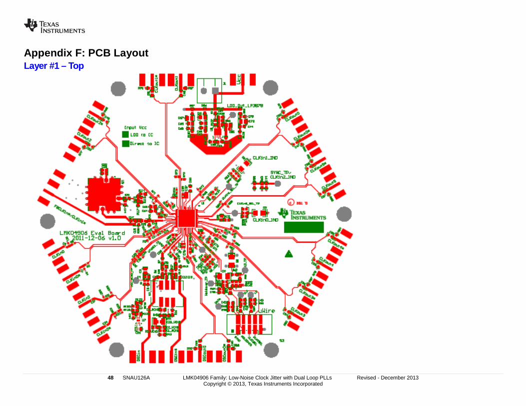
Appendix F: PCB Layout Layer #1 – Top
Revised - December 2013 LMK04906 Family: Low-Noise Clock Jitter with Dual Loop PLLs SNAU126A 49 Copyright © 2013, Texas Instruments Incorporated
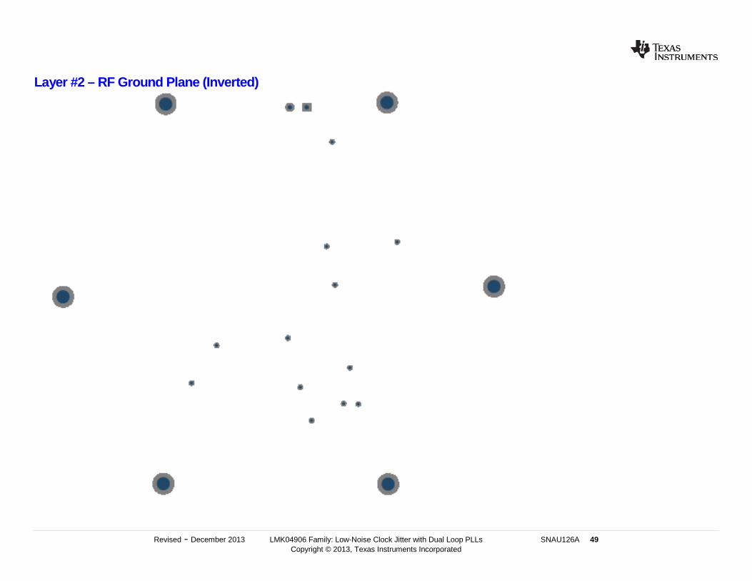
Layer #2 – RF Ground Plane (Inverted)

50 SNAU126A LMK04906 Family: Low-Noise Clock Jitter with Dual Loop PLLs Revised - December 2013 Copyright © 2013, Texas Instruments Incorporated
Layer #3 – Vcc Planes

Revised - December 2013 LMK04906 Family: Low-Noise Clock Jitter with Dual Loop PLLs SNAU126A 51 Copyright © 2013, Texas Instruments Incorporated
Layer #4 – Ground Plane (Inverted)

52 SNAU126A LMK04906 Family: Low-Noise Clock Jitter with Dual Loop PLLs Revised - December 2013 Copyright © 2013, Texas Instruments Incorporated
Layer # 5 – Vcc Planes 2
Revised - December 2013 LMK04906 Family: Low-Noise Clock Jitter with Dual Loop PLLs SNAU126A 53 Copyright © 2013, Texas Instruments Incorporated
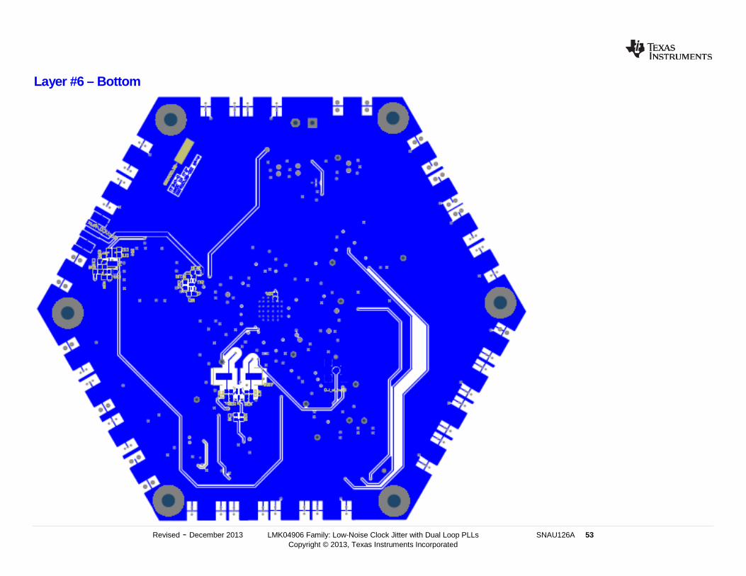
Layer #6 – Bottom

54 SNAU126A LMK04906 Family: Low-Noise Clock Jitter with Dual Loop PLLs Revised - December 2013 Copyright © 2013, Texas Instruments Incorporated
Layers #1 and 6 – Top and Bottom (Composite)
www.ti.com
Revised – December 2013 LMK04906 Family: Low-Noise Clock Jitter with Dual Loop PLLs SNAU126A 55 Copyright © 2013, Texas Instruments Incorporated
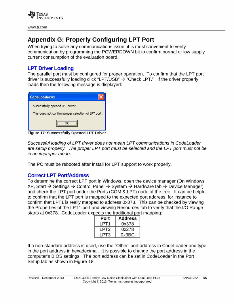
Appendix G: Properly Configuring LPT Port When trying to solve any communications issue, it is most convenient to verify communication by programming the POWERDOWN bit to confirm normal or low supply current consumption of the evaluation board. LPT Driver Loading The parallel port must be configured for proper operation. To confirm that the LPT port driver is successfully loading click “LPT/USB” “Check LPT.” If the driver properly loads then the following message is displayed:
Figure 17: Successfully Opened LPT Driver Successful loading of LPT driver does not mean LPT communications in CodeLoader are setup properly. The proper LPT port must be selected and the LPT port must not be in an improper mode. The PC must be rebooted after install for LPT support to work properly. Correct LPT Port/Address To determine the correct LPT port in Windows, open the device manager (On Windows XP, Start Settings Control Panel System Hardware tab Device Manager) and check the LPT port under the Ports (COM & LPT) node of the tree. It can be helpful to confirm that the LPT port is mapped to the expected port address, for instance to confirm that LPT1 is really mapped to address 0x378. This can be checked by viewing the Properties of the LPT1 port and viewing Resources tab to verify that the I/O Range starts at 0x378. CodeLoader expects the traditional port mapping:
Port Address LPT1 0x378 LPT2 0x278 LPT3 0x3BC
If a non-standard address is used, use the “Other” port address in CodeLoader and type in the port address in hexadecimal. It is possible to change the port address in the computer’s BIOS settings. The port address can be set in CodeLoader in the Port Setup tab as shown in Figure 18.

www.ti.com
56 SNAU126A LMK04906 Family: Low-Noise Clock Jitter with Dual Loop PLLs Revised – December 2013 Copyright © 2013, Texas Instruments Incorporated
Figure 18: Selecting the LPT Port Address Correct LPT Mode If communications are not working, then it is possible the LPT port mode is set improperly. It is recommended to use the simple, Output-only mode of the LPT port. This can be set in the BIOS of the computer. Common terms for this desired parallel port mode are “Normal,” “Output,” or “AT.” It is possible to enter BIOS setup during the initial boot up sequence of the computer. Legacy Board Port Setup If LPT communication with the LMK04906B EVM is required, then the following configuration should be followed for proper operation. Ensure the LPT port is configured correctly as well.

www.ti.com
Revised – December 2013 LMK04906 Family: Low-Noise Clock Jitter with Dual Loop PLLs SNAU126A 57 Copyright © 2013, Texas Instruments Incorporated
Appendix H: Troubleshooting Information If the evaluation board is not behaving as expected, the most likely issues are…
1) Board communication issue 2) Incorrect Programming of the device 3) Setup Error
Refer to this checklist for a practical guide on identifying/exposing possible issues. 1) Confirm Communications Refer to Appendix G: Properly Configuring LPT Port to troubleshoot this item. Remember to load device with Ctrl+L. 2) Confirm PLL1 operation/locking
1) Program LD_MUX = “PLL1_R/2” 2) Confirm that LD pin output is half the expected phase detector frequency of
PLL1. i. If not, examine CLKin_SEL programming. ii. If not, examine CLKin0_BUFTYPE / CLKin1_BUFTYPE. iii. If not, examine PLL1 register R programming. iv. If not, examine physical CLKin input.
3) Program LD_MUX = “PLL1_N /2” 4) Confirm that LD pin output is half the expected phase detector frequency of
PLL1. i. If not, examine PLL1 register N programming. ii. If not, examine physical OSCin input.
Naturally, the output frequency of the above two items, PLL 1 R Divider/2 and PLL 1 N Divider /2, on LD pin should be the same frequency.
5) Program LD_MUX = “PLL1_DLD” 6) Confirm the LD pin output is high.
i. If high, then PLL1 is locked, continue to PLL2 operation/locking. 7) If LD pin output is low, but the frequencies are the same, it is possible that
excessive leakage on Vtune pin is causing the digital lock detect to not activate. By default PLL2 waits for the digital lock detect to go high before allowing PLL2 and the integrated VCO to lock. Different VCXO models have different input leakage specifications. High leakage, low PLL1 phase detector frequencies, and low PLL1 charge pump current settings can cause the PLL1 charge pump to operate longer than the digital lock detect timeout which allows the device to lock, but prevents the digital lock detect from activating.
i. Redesign PLL1 loop filter with higher phase detector frequency ii. Redesign PLL1 loop filter with higher charge pump current iii. Isolate VCXO tuning input from PLL1 charge pump with an op amp.

www.ti.com
58 SNAU126A LMK04906 Family: Low-Noise Clock Jitter with Dual Loop PLLs Revised – December 2013 Copyright © 2013, Texas Instruments Incorporated
3) Confirm PLL2 operation/locking
1) Program LD_MUX = “PLL2_R/2” 2) Confirm that LD pin output is half the expected phase detector frequency of
PLL2. i. If not, examine PLL2_R programming. ii. If not, examine physical OSCin input.
3) Program LD_MUX = “PLL2_N/2” 4) Confirm that LD pin output is half the expected phase detector frequency of
PLL2. i. If not, confirm OSCin_FREQ is programmed to OSCin frequency. ii. If not, examine PLL2_N programming.
Naturally, the output frequency of the above two items should be the same frequency.
5) Program LD_MUX = “PLL2 DLD” 6) Confirm the LD pin output is high. 7) Program LD_MUX = “PLL1 & PLL2 DLD” 8) Confirm the LD pin output is high.

www.ti.com
Revised – December 2013 LMK04906 Family: Low-Noise Clock Jitter with Dual Loop PLLs SNAU126A 59 Copyright © 2013, Texas Instruments Incorporated
Appendix I: EVM Software and Communication Codeloader is the software used to communicate with the EVM (Please download the latest version from TI.com - http://www.ti.com/tool/codeloader). This EVM can be controlled through the uWire interface on board. There are two options in communicating with the uWire interface from the computer. OPTION 1
Open Codeloader.exe Click “Select Device” Click “Port Setup” tab Click “LPT” (in Communication Mode) OPTION 2

www.ti.com
60 SNAU126A LMK04906 Family: Low-Noise Clock Jitter with Dual Loop PLLs Revised – December 2013 Copyright © 2013, Texas Instruments Incorporated
The Adapter Board This table describes the pins configuration on the adapter board for each EVM board (See examples below table)
EVM Jumper Bank Code Loader Configuration A B C D E F G H
LMX2581 A4 B1 C2 E5 F1 G1 H1 BUFEN (pin 1), Trigger (pin 7) LMX2541 A4 C3 E4 F1 G1 H1 CE (pin 1), Trigger (pin 10) LMK0400x A0 C3 E5 F1 G1 H1 GOE (pin 7) LMK01000 A0 C1 E5 F1 G1 H1 GOE (pin 7) LMK030xx A0 C1 E5 F1 G1 H1 SYNC (pin 7) LMK02000 A0 C1 E5 F1 G1 H1 SYNC (pin 7) LMK0480x A0 B2 C3 E5 F0 G0 H1 Status_CLKin1 (pin 3) LMK04816/4906 A0 B2 C3 E5 F0 G0 H1 Status_CLKin1 (pin 3) LMK01801 A0 B4 C5 E2 F0 G0 H1 Test (pin 3), SYNC0 (pin 10) LMK0482x (prelease) A0 B5 C3 D2 E4 F0 G0 H1 CLKin1_SEL (pin 6), Reset (pin 10) LMX2531 A0 E5 F2 G1 H2 Trigger (pin 1) LMX2485/7 A0 C1 E5 F2 G1 H0 ENOSC (pin 7), CE (pin 10) LMK03200 A0 E5 F0 G0 H1 SYNC (pin 7) LMK03806 A0 C1 E5 F0 G0 H1 LMK04100 A0 C1 E5 F1 G1 H1
Example adapter configuration (LMK01801)
Open Codeloader.exe Click “Select Device” Click “Port Setup” Tab Click “USB” (in Communication Mode) *Remember to also make modifications in “Pin Configuration” Section according to Table above

IMPORTANT NOTICE
Texas Instruments Incorporated and its subsidiaries (TI) reserve the right to make corrections, enhancements, improvements and otherchanges to its semiconductor products and services per JESD46, latest issue, and to discontinue any product or service per JESD48, latestissue. Buyers should obtain the latest relevant information before placing orders and should verify that such information is current andcomplete. All semiconductor products (also referred to herein as “components”) are sold subject to TI’s terms and conditions of salesupplied at the time of order acknowledgment.TI warrants performance of its components to the specifications applicable at the time of sale, in accordance with the warranty in TI’s termsand conditions of sale of semiconductor products. Testing and other quality control techniques are used to the extent TI deems necessaryto support this warranty. Except where mandated by applicable law, testing of all parameters of each component is not necessarilyperformed.TI assumes no liability for applications assistance or the design of Buyers’ products. Buyers are responsible for their products andapplications using TI components. To minimize the risks associated with Buyers’ products and applications, Buyers should provideadequate design and operating safeguards.TI does not warrant or represent that any license, either express or implied, is granted under any patent right, copyright, mask work right, orother intellectual property right relating to any combination, machine, or process in which TI components or services are used. Informationpublished by TI regarding third-party products or services does not constitute a license to use such products or services or a warranty orendorsement thereof. Use of such information may require a license from a third party under the patents or other intellectual property of thethird party, or a license from TI under the patents or other intellectual property of TI.Reproduction of significant portions of TI information in TI data books or data sheets is permissible only if reproduction is without alterationand is accompanied by all associated warranties, conditions, limitations, and notices. TI is not responsible or liable for such altereddocumentation. Information of third parties may be subject to additional restrictions.Resale of TI components or services with statements different from or beyond the parameters stated by TI for that component or servicevoids all express and any implied warranties for the associated TI component or service and is an unfair and deceptive business practice.TI is not responsible or liable for any such statements.Buyer acknowledges and agrees that it is solely responsible for compliance with all legal, regulatory and safety-related requirementsconcerning its products, and any use of TI components in its applications, notwithstanding any applications-related information or supportthat may be provided by TI. Buyer represents and agrees that it has all the necessary expertise to create and implement safeguards whichanticipate dangerous consequences of failures, monitor failures and their consequences, lessen the likelihood of failures that might causeharm and take appropriate remedial actions. Buyer will fully indemnify TI and its representatives against any damages arising out of the useof any TI components in safety-critical applications.In some cases, TI components may be promoted specifically to facilitate safety-related applications. With such components, TI’s goal is tohelp enable customers to design and create their own end-product solutions that meet applicable functional safety standards andrequirements. Nonetheless, such components are subject to these terms.No TI components are authorized for use in FDA Class III (or similar life-critical medical equipment) unless authorized officers of the partieshave executed a special agreement specifically governing such use.Only those TI components which TI has specifically designated as military grade or “enhanced plastic” are designed and intended for use inmilitary/aerospace applications or environments. Buyer acknowledges and agrees that any military or aerospace use of TI componentswhich have not been so designated is solely at the Buyer's risk, and that Buyer is solely responsible for compliance with all legal andregulatory requirements in connection with such use.TI has specifically designated certain components as meeting ISO/TS16949 requirements, mainly for automotive use. In any case of use ofnon-designated products, TI will not be responsible for any failure to meet ISO/TS16949.
Products ApplicationsAudio www.ti.com/audio Automotive and Transportation www.ti.com/automotiveAmplifiers amplifier.ti.com Communications and Telecom www.ti.com/communicationsData Converters dataconverter.ti.com Computers and Peripherals www.ti.com/computersDLP® Products www.dlp.com Consumer Electronics www.ti.com/consumer-appsDSP dsp.ti.com Energy and Lighting www.ti.com/energyClocks and Timers www.ti.com/clocks Industrial www.ti.com/industrialInterface interface.ti.com Medical www.ti.com/medicalLogic logic.ti.com Security www.ti.com/securityPower Mgmt power.ti.com Space, Avionics and Defense www.ti.com/space-avionics-defenseMicrocontrollers microcontroller.ti.com Video and Imaging www.ti.com/videoRFID www.ti-rfid.comOMAP Applications Processors www.ti.com/omap TI E2E Community e2e.ti.comWireless Connectivity www.ti.com/wirelessconnectivity
Mailing Address: Texas Instruments, Post Office Box 655303, Dallas, Texas 75265Copyright © 2015, Texas Instruments Incorporated