low-cost ac solid-state relay with mosfets (rev. a) · pdf filea solid-state relay (ssr) is an...
TRANSCRIPT

Copyright © 2016, Texas Instruments Incorporated
Undervoltage lockout
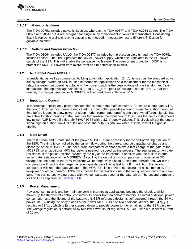
LP339(A)
DC power supply
2 × ATL431
Control logic
SN74LVC1G74LP339(B,C,D)
MOSFET switch
2 × CSD18541F524 VAC
Load
ON
OFF
1TIDUC87A–September 2016–Revised March 2017Submit Documentation Feedback
Copyright © 2016–2017, Texas Instruments Incorporated
Low-Cost AC Solid-State Relay With MOSFETs
TI DesignsLow-Cost AC Solid-State Relay With MOSFETs
DescriptionThe low-cost AC solid-state relay (SSR) withMOSFETs reference design is a single relayreplacement that enables efficient power managementfor a low-power alternative to standardelectromechanical relays in thermostat applications.This SSR reference design is the base model of theself-powered SSR providing a low-cost solution forlow-cost thermostats.
Resources
TIDA-01064 Design FolderATL431 Product FolderLP339 Product FolderSN74AUP1G74 Product FolderCSD18541F5 Product FolderTIDA-00377 Tools FolderTIDA-00751 Tools Folder
ASK Our E2E Experts
Features• No Clicking Sound• Low-Cost BOM• MOSFET Based Design for Fast ON/OFF
Switching• Self-Powered• Zero Power From Thermostat Battery• Inherent Snubber Circuit Reducing Voltage Spike
Created by Inductive Loads• Low Power and Quiescent Current Components• Undervoltage Protection
Applications• Thermostats• HVAC Systems• Building Automation
An IMPORTANT NOTICE at the end of this TI reference design addresses authorized use, intellectual property matters and otherimportant disclaimers and information.

Copyright © 2016, Texas Instruments Incorporated
Undervoltage lockout DC power supply
Control logic MOSFET switch 24 VAC
Load
ON
OFF
System Overview www.ti.com
2 TIDUC87A–September 2016–Revised March 2017Submit Documentation Feedback
Copyright © 2016–2017, Texas Instruments Incorporated
Low-Cost AC Solid-State Relay With MOSFETs
1 System Overview
1.1 System DescriptionA solid-state relay (SSR) is an electronic switching device that switches on or off when a small externalvoltage is applied across its control terminals. SSRs consist of an input logic to respond to an appropriateinput (control signal), a solid-state electronic switching device to switch power to the load circuitry, and acoupling mechanism to enable the control signal to activate this switch without mechanical parts. The SSRmay be designed to control either an AC or DC voltage or current load. It serves the same function as anelectromechanical relay, but has no moving parts.
SSRs use power semiconductor devices such as thyristors or transistors to switch currents up to 100 A.SSRs have fast switching speeds compared to electromechanical relays and have no physical contacts towear out. To apply an SSR, the user must consider their lower ability to withstand momentary overload,compared to electromechanical contacts, and their initial higher "on" state resistance. Unlike anelectromechanical relay, an SSR provides only limited switching arrangements (single-pole, single-throwswitching).
This SSR is a low-cost reference design for a single mechanical relay replacement in low-cost thermostatapplications, which only uses one switching relay. The SSR is self-powered through the AC line of theHVAC system and provides undervoltage lockout (UVLO). See Figure 1 for the block diagram.
Figure 1. TIDA-01064 SSR With MOSFETs Block Diagram
1.1.1 Choosing Between SSR Reference DesignsThe TI Designs portfolio has three available SSR reference designs: the TIDA-00377, TIDA-00751, andTIDA-01064. They differ in terms of power consumption, galvanic isolation, voltage and current protection,and cost. See Table 1 for a feature comparison between the three designs.
Table 1. Comparison of SSR Reference Designs
PARAMETER TIDA-00377 TIDA-00751 TIDA-01064Self-powered √ √Isolation √Snubber circuit √ √ √UVLO √ √OCP √Low cost √
1.1.1.1 Power ConsumptionThe TIDA-00377 and TIDA-01064 do not consume any power from the thermostat battery. They are self-powered and consume < 0.4 mA from the HVAC system. Alternatively, the TIDA-00751 consumes powerfrom the thermostat battery during both on and off-states. The SSR consumes 1.2 mA from the batteryduring on-state and < 0.2-mA during off-state.
www.ti.com System Overview
3TIDUC87A–September 2016–Revised March 2017Submit Documentation Feedback
Copyright © 2016–2017, Texas Instruments Incorporated
Low-Cost AC Solid-State Relay With MOSFETs
1.1.1.2 Galvanic IsolationThe TIDA-00751 includes galvanic isolation, whereas the TIDA-00377 and TIDA-01064 do not. The TIDA-00377 and TIDA-01064 are designed for single relay replacement in low-cost thermostats. Consideringthat it is replacing a single relay, isolation is not needed. If necessary, use a different TI Design forgalvanic isolation.
1.1.1.3 Voltage and Current ProtectionThe TIDA-01064 includes UVLO, the TIDA-00377 includes both protection circuits, and the TIDA-00751includes neither. The UVLO protects the low AC power supply, which also translates to the DC powersupply of the SSR. This will enable the self-powering feature. The overcurrent protection (OCP) is toprotect the MOSFET switch from overcurrent and to detect short circuits.
1.1.2 N-Channel Power MOSFETIn residential as well as commercial building automation application, 24 VAC is used as the standard powersupply voltage. When an SSR is used in thermostat applications as a replacement for the mechanicalrelay, the maximum operating voltage of the power switch is the peak voltage of one transformer. Takinginto account the input voltage variations (20 to 30 VAC), the peak DC voltage rises up to 43 V. For thatreason, this design uses power MOSFETs with a breakdown voltage of 60 V.
1.1.3 Input Logic ControlIn thermostat applications, power consumption is one of the main concerns. To ensure a long battery life,the control logic, in most cases a dedicated microcontroller, provides a control signal for a short period oftime before it goes in a low power or sleep mode. Turnon and turnoff signals are two different signals thatare active for short periods of the time. For that reason, the input control logic uses the Texas Instrumentslow-power AUP D-type flip-flop, SN74AUP1G74 with a 3.3-V supply voltage. This circuit will set the outputsignal high on a short, low-ON pulse and reset the output signal low when a short, low-OFF signal isapplied.
1.1.4 Gate DriverThe fast turnon and turnoff time of the power MOSFETs are necessary for the self-powering function ofthe SSR. The time is controlled by the current flow during the gate-to-source capacitance charge anddischarge of the MOSFETs. The open drain comparator cannot achieve a fast charge of the gate of theMOSFET so an additional NPN transistor is needed to speed up the process. The equivalent turnon gateresistance is the pullup resistor, divided by the hFE of the transistor, in addition with the built-in internalseries gate resistance of the MOSFETs. By pulling the output of two comparators to a negative DCvoltage rail, the base of the NPN transistor will be negatively biased turning the transistor off, while thecomparator will quickly discharge the gate capacitance allowing fast turnoff. In addition, the secondcomparator will keep the gate voltage of the MOSFET close to zero increasing the noise immunity. Thelow-power quad comparator LP339 was chosen for this function due to the low quiescent current and lowcost. This part serves two purposes with two comparators used for the gate driver. The second purpose isfor UVLO as explained in Section 1.1.6.
1.1.5 Power ManagementPower consumption is another main concern in thermostat applications because the circuitry, whichmakes up the thermostat control, consumes its power from an onboard battery. To avoid additional powerconsumption and the lifetime of the battery, this SSR reference design is self-powered through the 24 VACpower line. By using the body diodes of the power MOSFETs and two additional diodes, the 24 VAC isrectified to 33 VDC, which is further stepped down to provide power to the remaining of the SSR circuitry.The voltage regulation is performed by two low-power shunt regulators, ATL431, with a quiescent currentof 25 μA.
Copyright © 2016, Texas Instruments Incorporated
Undervoltage lockout
LP339(A)
DC power supply
2 × ATL431
Control logic
SN74LVC1G74LP339(B,C,D)
MOSFET switch
2 × CSD18541F524 VAC
Load
ON
OFF
System Overview www.ti.com
4 TIDUC87A–September 2016–Revised March 2017Submit Documentation Feedback
Copyright © 2016–2017, Texas Instruments Incorporated
Low-Cost AC Solid-State Relay With MOSFETs
1.1.6 Undervoltage LockoutTo properly regulate the voltage of the DC power supply, the input DC voltage must maintain a certainthreshold level. If the AC voltage or rectified AC voltage of the load (VDC) drops below the desired railvoltages, the shunt regulators will no longer be able to regulate, disabling the operability of the SSR. Dueto the nature of the DC power supply during the ON time of the MOSFETs, the DC supply capacitor willwant to fully discharge. To prevent this, a reference voltage is set on the UVLO to shortly turn off theMOSFETs when the minimum voltage is met and allows the DC supply capacitor to recharge withoutaffecting the load. This will keep VDC at a voltage where the shunt regulators can regulate properly. Toperform this function, one of the comparators from the LP339 is used. To use the UVLO as a controlsignal, a second comparator from the LP339 is used to perform a logic AND function between the UVLOand input control signals.
1.2 Key System Specifications
(1) Typical RθJA = 245°C/W
Table 2. Key System Specifications
SPECIFICATION VALUE DETAILSLogic input level 3.3 V See Section 1.1.3AC voltage input range 20 to 30 V See Section 1.1.1Maximum current 2 A (1) —Turnon and turnoff time < 1 µs See Section 4.2On-state current consumption (typ) 190 µA See Section 4.2Off-state current consumption (typ) 370 µA See Section 4.2Operating temperature 0°C to 60°C —Working environment Indoor building automation —
1.3 Block Diagram
Figure 2. TIDA-01064 SSR With MOSFET Block Diagram With Component List
1.4 Highlighted ProductsThe SSR reference design features the following devices:• CSD18541F5: 60-V N-Channel FemtoFET Power MOSFET• SN74AUP1G74: Low-Power Single Positive-Edge-Triggered D-Type Flip-Flop• ATL431: 2.5-V Low IQ Adjustable Precision Shunt Regulator• LP339: Low-Power Quad Differential Comparators
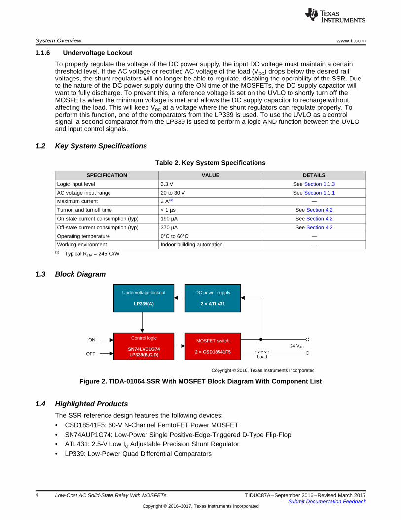
IAC
IAC+
IAC-
IAC
Reverse bias
Reverse bias
ON
ON
OFF
OFF
+
Copyright © 2016, Texas Instruments Incorporated
www.ti.com System Design Theory
5TIDUC87A–September 2016–Revised March 2017Submit Documentation Feedback
Copyright © 2016–2017, Texas Instruments Incorporated
Low-Cost AC Solid-State Relay With MOSFETs
2 System Design Theory
2.1 Basic SSR TheoryAn alternative to the electromechanical switch is an SSR with a MOSFET. SSRs are integrated electricalcircuits that act as a mechanical switch. The relays can be switched much faster and are not prone towear because of the absence of moving parts. Another advantage is that less current and voltage isneeded for SSRs to control high-voltage AC loads.
This design uses a two N-channel MOSFET topology serving two main functions. The first function is toperform the switching. By using two MOSFETs, both positive and negative current are allowed to flowduring the ON time, as shown in Figure 3a. During the OFF time, the body diodes block the current flowbecause the top and bottom body diode become reverse bias, as shown in Figure 3b.
Figure 3. Functionality of MOSFETs for (a) ON and (b) OFF Times
The second function of the two N-channel MOSFET topology is to self-power the system by assisting inthe AC voltage rectification. See Section 2.2 for more details.
DC
DC
i tV
C
´ DD =
P _DC AC FV 2 V 2 V= ´ - ´
Copyright © 2016, Texas Instruments Incorporated
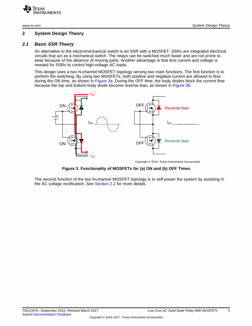
24 V120 V60 Hz
xxx
xxxx
L1
L2
+
33 V
PS and loadSolid state relay
System Design Theory www.ti.com
6 TIDUC87A–September 2016–Revised March 2017Submit Documentation Feedback
Copyright © 2016–2017, Texas Instruments Incorporated
Low-Cost AC Solid-State Relay With MOSFETs
2.2 Basic Power Management TheoryThe two MOSFET body diodes of the switch and two external diodes create a full-wave rectification circuitthat converts the AC power supply at the load to a DC voltage that can then be stepped down to desiredlevels. The control logic and gate driver are powered by the resulting DC voltage and therefore does notconsume any power from the thermostat battery.
Figure 4. Power Supply of SSR in HVAC System
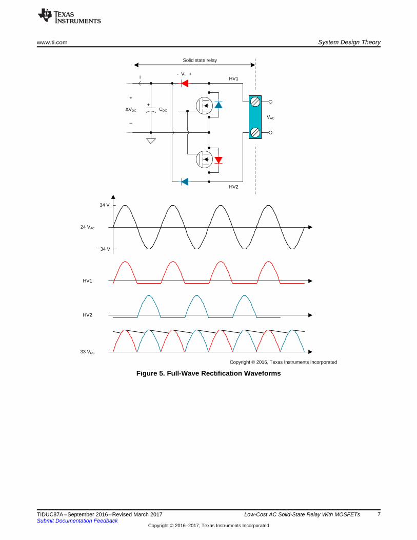
2.2.1 Full-Wave RectificationWhen the SSR is not active, the 24-VAC voltage from the HVAC system across HV1 and HV2 is rectifiedusing D1 and D2 in addition to the two body diodes of the MOSFETs. When the MOSFETs are off, theresulting full-wave rectified waveform has a peak DC voltage of 34 V, calculated by Equation 1.
(1)
With the addition of the capacitor, the rectified AC waveform is smoothed out providing a nominal averageDC voltage. The ripple of the DC voltage is determined by the value of the capacitor and the currentflowing through it over a period of time, as described in Equation 2.
(2)
The resulting waveforms are shown in Figure 5.
Copyright © 2016, Texas Instruments Incorporated
+
i
Solid state relay
HV1
HV2
CDC
+
ûVDC
_VAC
- VF +
34 V
í34 V
24 VAC
HV1
HV2
33 VDC
www.ti.com System Design Theory
7TIDUC87A–September 2016–Revised March 2017Submit Documentation Feedback
Copyright © 2016–2017, Texas Instruments Incorporated
Low-Cost AC Solid-State Relay With MOSFETs
Figure 5. Full-Wave Rectification Waveforms
Copyright © 2016, Texas Instruments Incorporated
VDC
R3
R1
R2
IFB
IREF
IKA
ATL431
VKA
+
VREF
-
VOUT
VGS - Gate-to-Source Voltage (V)
RD
S(o
n) -
On-
Sta
te R
esis
tanc
e (m
:)
0 2 4 6 8 10 12 14 16 18 2040
50
60
70
80
90
100
110
120
D007
TC = 25°C, I D = 1 ATC = 125°C, I D = 1 A
System Design Theory www.ti.com
8 TIDUC87A–September 2016–Revised March 2017Submit Documentation Feedback
Copyright © 2016–2017, Texas Instruments Incorporated
Low-Cost AC Solid-State Relay With MOSFETs
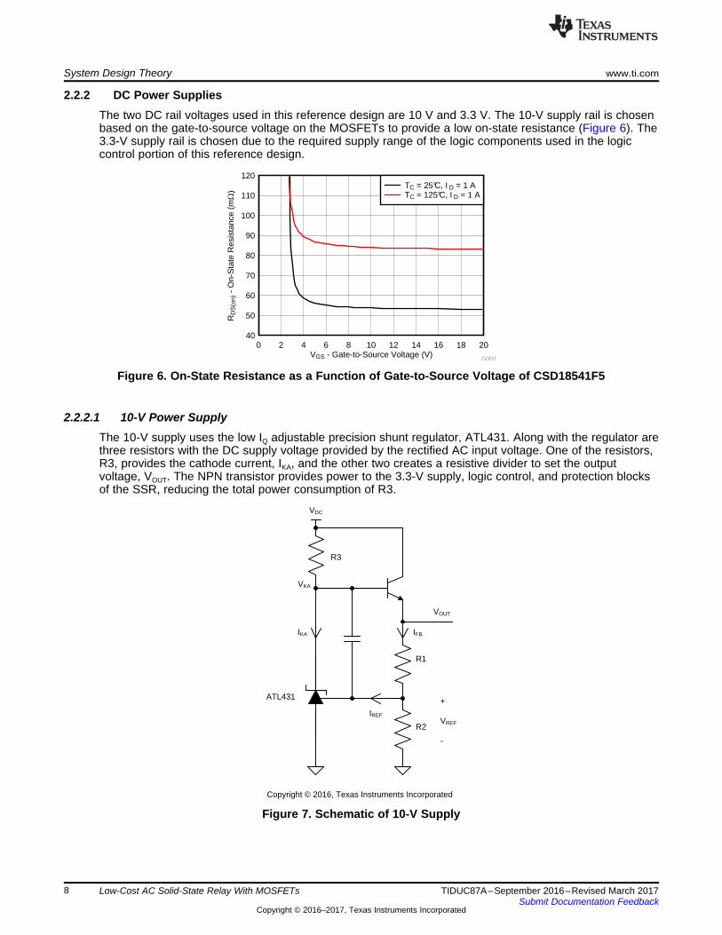
2.2.2 DC Power SuppliesThe two DC rail voltages used in this reference design are 10 V and 3.3 V. The 10-V supply rail is chosenbased on the gate-to-source voltage on the MOSFETs to provide a low on-state resistance (Figure 6). The3.3-V supply rail is chosen due to the required supply range of the logic components used in the logiccontrol portion of this reference design.
Figure 6. On-State Resistance as a Function of Gate-to-Source Voltage of CSD18541F5
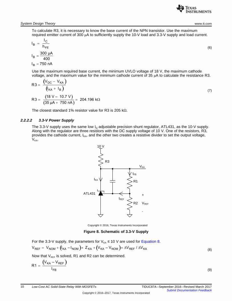
2.2.2.1 10-V Power SupplyThe 10-V supply uses the low IQ adjustable precision shunt regulator, ATL431. Along with the regulator arethree resistors with the DC supply voltage provided by the rectified AC input voltage. One of the resistors,R3, provides the cathode current, IKA, and the other two creates a resistive divider to set the outputvoltage, VOUT. The NPN transistor provides power to the 3.3-V supply, logic control, and protection blocksof the SSR, reducing the total power consumption of R3.
Figure 7. Schematic of 10-V Supply

( )2.4899 V
R2 1.264 M2 µA – 30 nA
= = W
( )10V – 2.4899 VR1 3.755 M
2 µA= = W
( ) ( )REF
REF
V 2.5 V 20 µA – 1 mA 0.05 10.6 V – 10 V – 0.1 mV / V – 10.5 mV
V 2.4899 V
= + ´ W + ´
=
( )REF
FB REF
VR2
I – I
=
( )KA REF
FB
V – V
R1I
=
( ) ( )REF NOM KA NOM KA KAV V I – I x Z V – 10 –0.1 mV / V – 10.5 mV= + + ´
www.ti.com System Design Theory
9TIDUC87A–September 2016–Revised March 2017Submit Documentation Feedback
Copyright © 2016–2017, Texas Instruments Incorporated
Low-Cost AC Solid-State Relay With MOSFETs
Table 3. ATL431 Electrical Characteristics Over Recommended Operating Conditions 25˚C
PARAMETER TEST CONDITIONS MIN TYP MAX UNITVREF Reference voltage VKA = Vref, IKA = 1 mA 2475 2500 2525 mV
VI(dev)
Deviation of reference inputvoltage over full temperaturerange
VKA = VREF,IKA = 1 mA,
ATL43xAI; TA =–40°C to 85°C 5 15
mVATL43xAQ; TA =–40°C to 125°C 6 34
ΔVREF / ΔVKA
Ratio of change in referencevoltage to the change incathode voltage
IKA = 1 mAΔVKA = 10 V – VREF –0.4 –2.7
mV/VΔVKA = 36 V – 10 V –0.1 –2
IREF Reference input current IKA = 1 mA, R1 = 10 kΩ, R2 = ∞ 30 150 nA
II(dev)
Deviation of reference inputcurrent over full temperaturerange
IKA = 1 mA, R1 = 10 kΩ, R2 = ∞ 20 50 nA
IMINMinimum cathode current forregulation VKA = VREF 20 35 µA
IOFF Off-state cathode current VKA = 36 V, VREF = 0 0.05 0.2 µA|zKA| Dynamic impedance VKA = VREF, f ≤ 1 kHz, IKA = 1 to 100 mA 0.05 0.3 Ω
Table 3 specifies when VKA = VREF and IKA is 1 mA the nominal VREF, (labeled as VNOM) is 2.5 V. Thereference voltage varies with cathode voltage at two different rates: –0.4 mV/V from VREF to 10 V, and –0.1mV/V above 10 V. The reference pin current is 30 nA.
The ZKA parameter offsets VREF by (IKA – INOM) × ZKA. In addition, the ΔVREF/ΔVKA parameter offsets VREF byeither –0.4 mV × (VKA – 2.5 V) if VKA ≤ 10 V, or –10.5 mV – 0.1 mV/V × (VKA – 10 V) if VKA > 10 V. The"–10.5 mV" constant is the VREF offset as VKA changes from VNOM to 10 V, (10 V –2.5 V) × –0.4 mV/V.
For the 10-V supply, the parameters for VKA > 10 V are used for Equation 3 because VKA = 10.6 V due tothe voltage drop across the NPN transistor.
(3)
Now that VREF is solved, R1 and R2 can be determined.
(4)
(5)
NOTE: R2 has less current than R1.
The design goal is to set the cathode of the ATL431 to 10.6 V by providing a minimum cathode current of20 μA, and a feedback current and resistor bridge that will keep VKA within a narrow supply range of ±2%to 3%. The following parameters are calculated using the formula derived in the general example for VKA >10 V.
The closest standard 1% resistor value for R1 is 3.74 kΩ. A value of 1.3 MΩ is chosen for R2 to achievethe VKA narrow supply range 10 V ± 2% to 3%.
( )KA REF
FB
V – V
R1I
=
( ) ( )REF NOM KA NOM KA KA NOM REF KAV V I – I Z V – V V / V= + ´ + ´ D D
Copyright © 2016, Texas Instruments Incorporated
10 V
R3
R1
R2
IFB
IREF
IKA
ATL431
VKA
+
VREF
-
( )
( )
18 V – 10.7 VR3 204.196 k
35 µA 750 nA= = W
+
( )( )
DC KA
KA B
V VR3
I I
-=
+
B
B
300 µAI
400
I 750 nA
=
=
C
B
FE
II
h=
System Design Theory www.ti.com
10 TIDUC87A–September 2016–Revised March 2017Submit Documentation Feedback
Copyright © 2016–2017, Texas Instruments Incorporated
Low-Cost AC Solid-State Relay With MOSFETs
To calculate R3, it is necessary to know the base current of the NPN transistor. Use the maximumrequired emitter current of 300 μA to sufficiently supply the 10-V load and 3.3-V supply and load current.
(6)
Use the maximum required base current, the minimum UVLO voltage of 18 V, the maximum cathodevoltage, and the maximum value for the minimum cathode current of 35 μA to calculate the resistance R3.
(7)
The closest standard 1% resistor value for R3 is 205 kΩ.
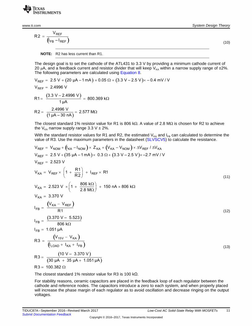
2.2.2.2 3.3-V Power SupplyThe 3.3-V supply uses the same low IQ adjustable precision shunt regulator, ATL431, as the 10-V supply.Along with the regulator are three resistors with the DC supply voltage of 10 V. One of the resistors, R3,provides the cathode current, IKA, and the other two creates a resistive divider to set the output voltage,VKA.
Figure 8. Schematic of 3.3-V Supply
For the 3.3-V supply, the parameters for VKA ≤ 10 V are used for Equation 8.
(8)
Now that VREF is solved, R1 and R2 can be determined.
(9)
( )
( )
10 V – 3.370 VR3
30 µA 35 µA 1.051 µA
R3 100.382
=+ +
= W
( )( )
15V KA
LOAD KA FB
V VR3
I I I
-=
+ +
( )FB
FB
3.370 V – 5.523I
806 k
I 1.051 µA
=W
=
( )KA REF
FB
V V
IR1
-=
KA
KA
806 kV 2.523 V 1 150 nA 806 k
2.8 M
V 3.370 V
Wæ ö= ´ + + ´ Wç ÷Wè ø
=
KA REF REF
R1V V 1 I R1
R2
æ ö= ´ + + ´ç ÷
è ø
( ) ( )( ) ( )
REF NOM KA NOM KA KA NOM REF KA
REF
REF
V V I – I Z V – V V / V
V 2.5 V 35 µA – 1 mA 0.3 3.3 V – 2.5 V –2.7 mV / V
V 2.523 V
= + ´ + ´ D D
= + ´ W + ´
=
( )2.4996 V
R2 2.577 M1 µA – 30 nA
= = W
( )3.3 V – 2.4996 VR1 800.369 k
1 µA= = W
( ) ( )REF
REF
V 2.5 V 20 µA – 1 mA 0.05 3.3 V – 2.5 V – 0.4 mV / V
V 2.4996 V
= + ´ W + ´
=
( )REF
FB REF
VR2
I – I
=
www.ti.com System Design Theory
11TIDUC87A–September 2016–Revised March 2017Submit Documentation Feedback
Copyright © 2016–2017, Texas Instruments Incorporated
Low-Cost AC Solid-State Relay With MOSFETs
(10)
NOTE: R2 has less current than R1.
The design goal is to set the cathode of the ATL431 to 3.3 V by providing a minimum cathode current of20 μA, and a feedback current and resistor divider that will keep VKA within a narrow supply range of ±2%.The following parameters are calculated using Equation 8.
The closest standard 1% resistor value for R1 is 806 kΩ. A value of 2.8 MΩ is chosen for R2 to achievethe VKA narrow supply range 3.3 V ± 2%.
With the standard resistor values for R1 and R2, the estimated VKA and IFB can calculated to determine thevalue of R3. Use the maximum parameters in the datasheet (SLVSCV5) to calculate the resistance.
(11)
(12)
(13)
The closest standard 1% resistor value for R3 is 100 kΩ.
For stability reasons, ceramic capacitors are placed in the feedback loop of each regulator between thecathode and reference nodes. The capacitors introduce a zero to each system, and when properly placedwill increase the phase margin of each regulator as to avoid oscillation and decrease ringing on the outputvoltages.
Copyright © 2016, Texas Instruments Incorporated
+
-+
UVLO
+
+
10 V
3.3 V
VDC
10 V
ATL431LP339
ATL431
+
+ +
ûVDC
-
CDC
CUVLO
RUVLO
iS
4.3 V
System Design Theory www.ti.com
12 TIDUC87A–September 2016–Revised March 2017Submit Documentation Feedback
Copyright © 2016–2017, Texas Instruments Incorporated
Low-Cost AC Solid-State Relay With MOSFETs
2.3 MOSFET SelectionLow-cost thermostats can be connected up to two separate 24-VAC connections. This low-cost SSRreference design is focused towards thermostats that are connected to a single transformer. For theconnection of two transformers, see the TIDA-00377 design. A standard 24-VAC power relay with a currentrating of 40 A has a coil resistance of 660 Ω. The 120- to 24-VAC transformer output voltage can rangefrom 20 to 30 VAC. Therefore, each MOSFET must be able to handle a drain-to-source voltage and currentof 43 VDC and 0.12 A, respectively. The CSD18541F5 was chosen for its 60-V drain-to-source voltage andpackage size and cost.
When the SSR is used to turn on and off the inductive load, take care to limit overvoltage spikes duringthe turnoff process. The DC supply capacitor and external rectification diodes create a snubber circuit toabsorb the energy from inductive load during turnoff. When the switch is turned off, the current from theinductive load is interrupted, causing the voltage to spike. For additional precaution, a transient voltagesuppression (TVS) diode is added across the MOSFETs. For the DC application, unidirectional TVS issufficient where for AC application, a bidirectional TVS is needed.
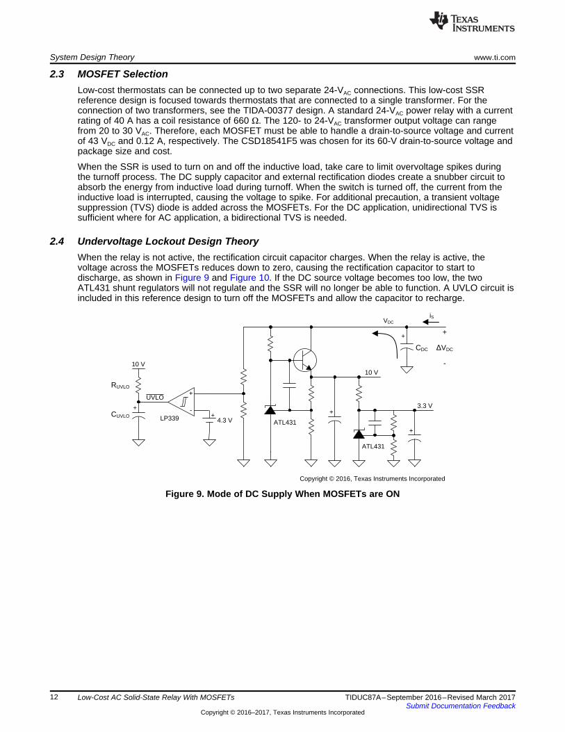
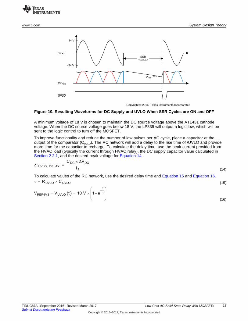
2.4 Undervoltage Lockout Design TheoryWhen the relay is not active, the rectification circuit capacitor charges. When the relay is active, thevoltage across the MOSFETs reduces down to zero, causing the rectification capacitor to start todischarge, as shown in Figure 9 and Figure 10. If the DC source voltage becomes too low, the twoATL431 shunt regulators will not regulate and the SSR will no longer be able to function. A UVLO circuit isincluded in this reference design to turn off the MOSFETs and allow the capacitor to recharge.
Figure 9. Mode of DC Supply When MOSFETs are ON
( )t
REF4V3 UVLOV V t 10 V 1 e-
tæ öç ÷= = ´ -ç ÷è ø
UVLO UVLOR Ct = ´
DC DCUVLO _DELAY
S
C Vt
i
´ DD =
Copyright © 2016, Texas Instruments Incorporated
34 V
í34 V
24 VAC
33 VDC
UVLO
SSRTurn-on
VREF
www.ti.com System Design Theory
13TIDUC87A–September 2016–Revised March 2017Submit Documentation Feedback
Copyright © 2016–2017, Texas Instruments Incorporated
Low-Cost AC Solid-State Relay With MOSFETs
Figure 10. Resulting Waveforms for DC Supply and UVLO When SSR Cycles are ON and OFF
A minimum voltage of 18 V is chosen to maintain the DC source voltage above the ATL431 cathodevoltage. When the DC source voltage goes below 18 V, the LP339 will output a logic low, which will besent to the logic control to turn off the MOSFET.
To improve functionality and reduce the number of low pulses per AC cycle, place a capacitor at theoutput of the comparator (CUVLO). The RC network will add a delay to the rise time of /UVLO and providemore time for the capacitor to recharge. To calculate the delay time, use the peak current provided fromthe HVAC load (typically the current through HVAC relay), the DC supply capacitor value calculated inSection 2.2.1, and the desired peak voltage for Equation 14.
(14)
To calculate values of the RC network, use the desired delay time and Equation 15 and Equation 16.(15)
(16)

Copyright © 2016, Texas Instruments Incorporated
10 V 10 V
+
-
+
PRE
CLR
Q
QD
LP339(C)
SN74AUP1G74
CLK
ON
OFF
Gate
Q
EN
Drive
HV1
HV2
+
-
+
10 V
+
-
+
+
-
+
LP339(D)LP339(C)
UVLO LP339(A)
+
4.3V
4.3 V
4.3 V
1.65 V
3.3 V
System Design Theory www.ti.com
14 TIDUC87A–September 2016–Revised March 2017Submit Documentation Feedback
Copyright © 2016–2017, Texas Instruments Incorporated
Low-Cost AC Solid-State Relay With MOSFETs
2.5 Control Logic Design TheoryThe control logic circuitry uses short, LOW logic level pulses at the inputs of the D-type flip-flop,SN74AUP1G74, to turn on and off the MOSFETs. See Table 4 for the logic levels on output Q inreference to the input levels of /PRE and /CLR. Output Q is sent to a comparator whose output isconnected to the output of the UVLO comparator, as shown in Figure 11. The connection of thecomparator outputs performs an AND function between the flip-flop and UVLO output signals. Theresulting voltage level, EN, is sent to the two comparators of the gate driving network.
Figure 11. Control Logic and Gate Driver Schematic
Table 4. SN74AUP1G74 Logic Levels for /PRE, /CLR, and Q
/PRE /CLR CLK D QL H X X HH L X X LH H ↑ L L
When the SSR is initially connected to the power source, the flip-flop will start in an unknown state. Toinitialize the flip-flop in the off-state, connect an RC network at the active rising edge CLK input andconnect D to GND. After the rail voltages are stable, the signal at the CLK input will increase dependingon the time constant of the network. When the RC signal passes the VIH threshold of the CLK input, the Qoutput will be set to a logic level low setting the SSR in an off-state.
Copyright © 2016, Texas Instruments Incorporated
10 V 10 V
+
-
+
LP339
GateEN
Drive
+
RCB
½ RG
2CGS
+
-
+
LP339EN
4.3 V
4.3 V
www.ti.com System Design Theory
15TIDUC87A–September 2016–Revised March 2017Submit Documentation Feedback
Copyright © 2016–2017, Texas Instruments Incorporated
Low-Cost AC Solid-State Relay With MOSFETs
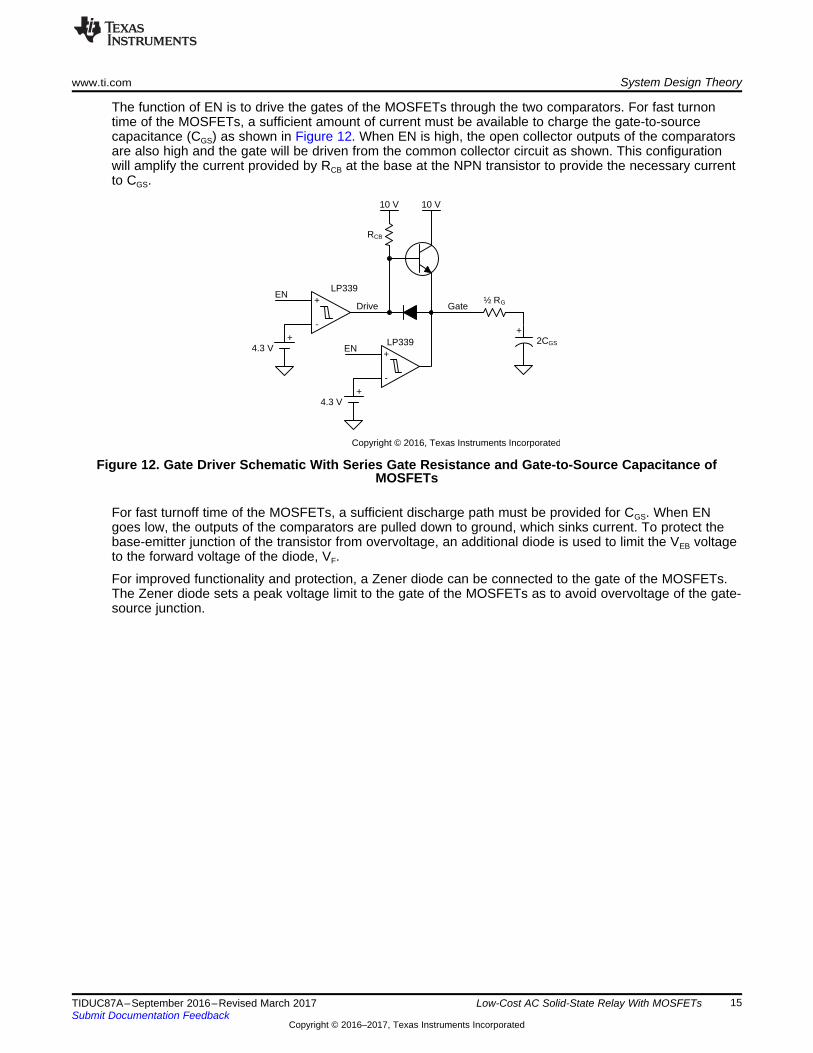
The function of EN is to drive the gates of the MOSFETs through the two comparators. For fast turnontime of the MOSFETs, a sufficient amount of current must be available to charge the gate-to-sourcecapacitance (CGS) as shown in Figure 12. When EN is high, the open collector outputs of the comparatorsare also high and the gate will be driven from the common collector circuit as shown. This configurationwill amplify the current provided by RCB at the base at the NPN transistor to provide the necessary currentto CGS.
Figure 12. Gate Driver Schematic With Series Gate Resistance and Gate-to-Source Capacitance ofMOSFETs
For fast turnoff time of the MOSFETs, a sufficient discharge path must be provided for CGS. When ENgoes low, the outputs of the comparators are pulled down to ground, which sinks current. To protect thebase-emitter junction of the transistor from overvoltage, an additional diode is used to limit the VEB voltageto the forward voltage of the diode, VF.
For improved functionality and protection, a Zener diode can be connected to the gate of the MOSFETs.The Zener diode sets a peak voltage limit to the gate of the MOSFETs as to avoid overvoltage of the gate-source junction.
HV1 and HV2
PRE
CLR
Q
EN
Drive
Gate
Turnon Turnoff
0 V
0 V
0 V
0 V
0 V
0 V
0 V
0 V
0 V
0 V
0 V
0 V
0 V
0 V
0 V
0 V
UVLO
HV1 and HV2
PRE
CLR
Q
EN
Drive
Gate
UVLO
System Design Theory www.ti.com
16 TIDUC87A–September 2016–Revised March 2017Submit Documentation Feedback
Copyright © 2016–2017, Texas Instruments Incorporated
Low-Cost AC Solid-State Relay With MOSFETs
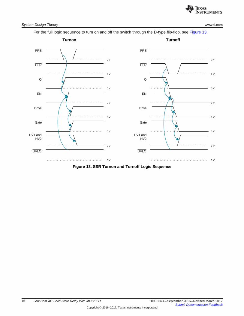
For the full logic sequence to turn on and off the switch through the D-type flip-flop, see Figure 13.
Figure 13. SSR Turnon and Turnoff Logic Sequence

www.ti.com Getting Started Hardware
17TIDUC87A–September 2016–Revised March 2017Submit Documentation Feedback
Copyright © 2016–2017, Texas Instruments Incorporated
Low-Cost AC Solid-State Relay With MOSFETs
3 Getting Started Hardware
3.1 Board OverviewFor ease of use, all of the components, headers, and test points are located on the top side of the board,as shown in Figure 14. The signal chain starts on the left side of the board and moves to the right side ofthe board in a linear fashion. The input headers, J5 and J7, are located on the left edge of the board hasconnection points ON and OFF for active logic level LOW inputs of the D-type flip-flop. To the right ofthose two headers is J9, which provides the option to use the enable signal from the D-type flip-flop or anexternally applied enable signal. The top-most headers connect the 3.3-VDC supply (J4) and 10-VDC supply(J3) rails to the corresponding loads. The three remaining two pin headers in the center of the boardconnect the rectified ac load voltage to the DC power supply (J2), rectified AC load voltage to the input ofthe UVLO (J2), and the output of the UVLO to the gate driver (J6). On the far right is the terminal block(J5), which connects the circuit to the 24-VAC HVAC load. The eight surface mount test points provideaccess to the signal chain and ground.
Figure 14. TIDA-01064 Reference Design Hardware
Getting Started Hardware www.ti.com
18 TIDUC87A–September 2016–Revised March 2017Submit Documentation Feedback
Copyright © 2016–2017, Texas Instruments Incorporated
Low-Cost AC Solid-State Relay With MOSFETs
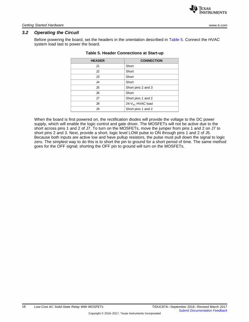
3.2 Operating the CircuitBefore powering the board, set the headers in the orientation described in Table 5. Connect the HVACsystem load last to power the board.
Table 5. Header Connections at Start-up
HEADER CONNECTIONJ1 ShortJ2 ShortJ3 ShortJ4 ShortJ5 Short pins 2 and 3J6 ShortJ7 Short pins 1 and 2J8 24-VAC HVAC loadJ9 Short pins 1 and 2
When the board is first powered on, the rectification diodes will provide the voltage to the DC powersupply, which will enable the logic control and gate driver. The MOSFETs will not be active due to theshort across pins 1 and 2 of J7. To turn on the MOSFETs, move the jumper from pins 1 and 2 on J7 toshort pins 2 and 3. Next, provide a short, logic level LOW pulse to ON through pins 1 and 2 of J5.Because both inputs are active low and have pullup resistors, the pulse must pull down the signal to logiczero. The simplest way to do this is to short the pin to ground for a short period of time. The same methodgoes for the OFF signal; shorting the OFF pin to ground will turn on the MOSFETs.
www.ti.com Testing and Results
19TIDUC87A–September 2016–Revised March 2017Submit Documentation Feedback
Copyright © 2016–2017, Texas Instruments Incorporated
Low-Cost AC Solid-State Relay With MOSFETs
4 Testing and Results
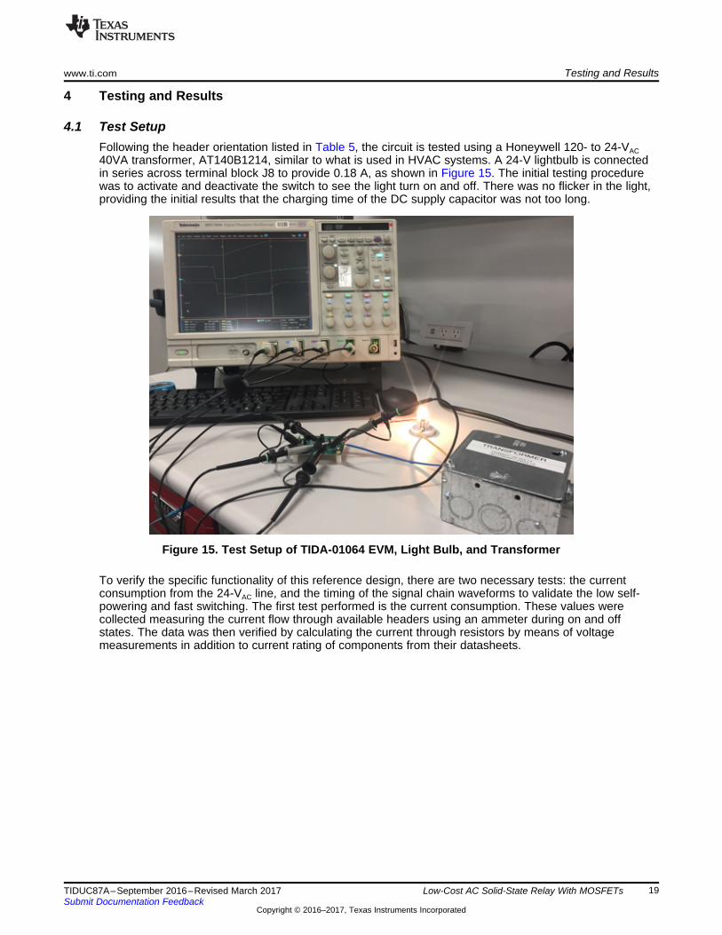
4.1 Test SetupFollowing the header orientation listed in Table 5, the circuit is tested using a Honeywell 120- to 24-VAC40VA transformer, AT140B1214, similar to what is used in HVAC systems. A 24-V lightbulb is connectedin series across terminal block J8 to provide 0.18 A, as shown in Figure 15. The initial testing procedurewas to activate and deactivate the switch to see the light turn on and off. There was no flicker in the light,providing the initial results that the charging time of the DC supply capacitor was not too long.
Figure 15. Test Setup of TIDA-01064 EVM, Light Bulb, and Transformer
To verify the specific functionality of this reference design, there are two necessary tests: the currentconsumption from the 24-VAC line, and the timing of the signal chain waveforms to validate the low self-powering and fast switching. The first test performed is the current consumption. These values werecollected measuring the current flow through available headers using an ammeter during on and offstates. The data was then verified by calculating the current through resistors by means of voltagemeasurements in addition to current rating of components from their datasheets.

Testing and Results www.ti.com
20 TIDUC87A–September 2016–Revised March 2017Submit Documentation Feedback
Copyright © 2016–2017, Texas Instruments Incorporated
Low-Cost AC Solid-State Relay With MOSFETs
The second test is to measure the timing of the control signals, which includes four sets of signals. Thefirst is charging time of the DC supply capacitor. This is seen by probing J1, J6, TP4, and AC1/AC2 asshown in Figure 16.
Figure 16. Probe Connections for Signal Chain Waveforms
The second and third signals are to check the turnon and turnoff delay of the MOSFETs. The turnon andturnoff functionality has been verified visually by the lightbulb, but it is important to verify the speed of theswitching as to efficiently charge the DC supply capacitor during active time. The waveforms captured areON, TP3, TP4, and AC1/AC2, which can be found in Figure 20 and Figure 21 in Section 4.2.

Cur
rent
(P
A)
0
50
100
150
200
DC Power Supply UVLO Control Logic
179.4
18.52
169.41
D002
Cur
rent
(P
A)
0
25
50
75
100
125
DC Power Supply UVLO Control Logic
111.11
17.61
57.91
D001
www.ti.com Testing and Results
21TIDUC87A–September 2016–Revised March 2017Submit Documentation Feedback
Copyright © 2016–2017, Texas Instruments Incorporated
Low-Cost AC Solid-State Relay With MOSFETs
4.2 Test DataThe total steady-state current consumption for both on and off times are found in Table 6. The steady-state currents for each block of the SSR for both on and off times are shown in Figure 17 and Figure 18.
Table 6. Total Steady-State Current Consumption
STATE CURRENT (µA)ON time 186.63OFF time 367.33
Figure 17. Steady-State Current Consumption During ON Time
Figure 18. Steady-State Current Consumption During OFF Time
Testing and Results www.ti.com
22 TIDUC87A–September 2016–Revised March 2017Submit Documentation Feedback
Copyright © 2016–2017, Texas Instruments Incorporated
Low-Cost AC Solid-State Relay With MOSFETs
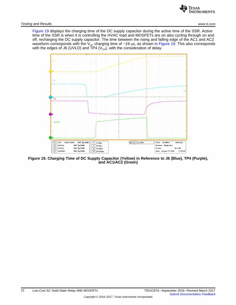
Figure 19 displays the charging time of the DC supply capacitor during the active time of the SSR. Activetime of the SSR is when it is controlling the HVAC load and MOSFETs are on also cycling through on andoff, recharging the DC supply capacitor. The time between the rising and falling edge of the AC1 and AC2waveform corresponds with the VDC charging time of ~19 μs, as shown in Figure 19. This also correspondswith the edges of J6 (UVLO) and TP4 (VGS), with the consideration of delay.
Figure 19. Charging Time of DC Supply Capacitor (Yellow) in Reference to J6 (Blue), TP4 (Purple),and AC1/AC2 (Green)
www.ti.com Testing and Results
23TIDUC87A–September 2016–Revised March 2017Submit Documentation Feedback
Copyright © 2016–2017, Texas Instruments Incorporated
Low-Cost AC Solid-State Relay With MOSFETs
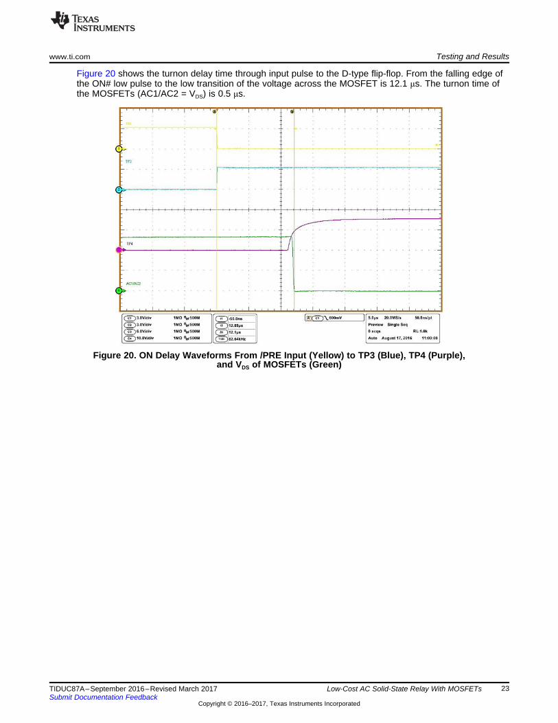
Figure 20 shows the turnon delay time through input pulse to the D-type flip-flop. From the falling edge ofthe ON# low pulse to the low transition of the voltage across the MOSFET is 12.1 μs. The turnon time ofthe MOSFETs (AC1/AC2 = VDS) is 0.5 μs.
Figure 20. ON Delay Waveforms From /PRE Input (Yellow) to TP3 (Blue), TP4 (Purple),and VDS of MOSFETs (Green)

Testing and Results www.ti.com
24 TIDUC87A–September 2016–Revised March 2017Submit Documentation Feedback
Copyright © 2016–2017, Texas Instruments Incorporated
Low-Cost AC Solid-State Relay With MOSFETs
Figure 21 shows the turnoff delay time through input pulse to the D-type flip-flop. The delay time from thefalling edge of the OFF low pulse to the low transition of the voltage across the MOSFETs is 4.6 μs. Theturnoff time of the MOSFETs (AC1/AC2 = VDS) is 0.75 μs.
Figure 21. OFF Delay Waveforms From /CLR Input (Yellow) to TP3 (Blue), TP4 (Purple),and VDS of MOSFETs (Green)

www.ti.com Design Files
25TIDUC87A–September 2016–Revised March 2017Submit Documentation Feedback
Copyright © 2016–2017, Texas Instruments Incorporated
Low-Cost AC Solid-State Relay With MOSFETs
5 Design Files
5.1 SchematicsTo download the schematics, see the design files at TIDA-01064.
5.2 Bill of MaterialsTo download the bill of materials (BOM), see the design files at TIDA-01064.
5.3 PCB Layout RecommendationsA careful PCB layout is critical and extremely important in a high-current, fast-switching circuit to provideappropriate device operation and design robustness. As with all switching power supplies, pay attention todetail in the layout to save time in troubleshooting later on.
5.3.1 Layout PrintsTo download the layer plots, see the design files at TIDA-01064.
5.4 Altium ProjectTo download the Altium project files, see the design files at TIDA-01064.
5.5 Gerber FilesTo download the Gerber files, see the design files at TIDA-01064.
5.6 Assembly DrawingsTo download the assembly drawings, see the design files at TIDA-01064.
6 Related Documentation
1. Texas Instruments, Designing with the "Advanced" TL431, ATL431, Application Report (SLVA685)2. Texas Instruments, Setting the Shunt Voltage on an Adjustable Shunt Regulator, Application Report
(SLVA445)3. Texas Instruments, Compensation Design With TL431 for UCC28600, Application Report (SLUA671)4. Texas Instruments, TI E2E Community: Industrial Strength, Click! Clack! What’s the setback in your
thermostat?, (2016, June 28) Retrieved fromhttp://e2e.ti.com/blogs_/b/industrial_strength/archive/2016/06/28/click-clack-what-s-the-setback-in-your-thermostat
5. Texas Instruments, TI E2E Community: Industrial Strength, A modern approach to solid-state relaydesign, (2016, July 26) Retrieved fromhttps://e2e.ti.com/blogs_/b/industrial_strength/archive/2016/07/26/a-modern-approach-to-solid-state-relay-design
6. Texas Instruments, TI E2E Community: Industrial Strength, How to power your thermostat using solidstate relays, (2016, August 11) Retrieved fromhttps://e2e.ti.com/blogs_/b/industrial_strength/archive/2016/08/11/how-to-power-your-thermostat-using-solid-state-relays
7. JEDEC Solid State Technology Association. (2006). Interface Standard for nominal 3 V/3.3 V SupplyDigital Integrated Circuits (JESD8C.01). Arlington, VA : JEDEC Solid State Technology Association

About the Authors www.ti.com
26 TIDUC87A–September 2016–Revised March 2017Submit Documentation Feedback
Copyright © 2016–2017, Texas Instruments Incorporated
Low-Cost AC Solid-State Relay With MOSFETs
6.1 TrademarksAll trademarks are the property of their respective owners.
7 About the AuthorsTATTIANA DAVENPORT is a systems designer at Texas Instruments, where she is responsible fordeveloping reference designs in the industrial segment. Tattiana has experience with general analog,power systems and electronics, and automotive ADAS applications. Tattiana earned her bachelor ofscience and master of science in electrical engineering from California Polytechnic State University in SanLuis Obispo, CA. Tattiana is also a member of the Society of Women Engineers (SWE).
MIROSLAV OLJACA is the End Equipment Lead for building automation applications and systemsolutions. Miro has 30 years of engineering experience and has been granted at least a dozen patents,several related to high performance signal processing, and he has written many articles on the subject.Miro received his BSEE and MSEE from the University of Belgrade, Serbia.

www.ti.com Revision A History
27TIDUC87A–September 2016–Revised March 2017Submit Documentation Feedback
Copyright © 2016–2017, Texas Instruments Incorporated
Revision History
Revision A HistoryNOTE: Page numbers for previous revisions may differ from page numbers in the current version.
Changes from Original (September 2016) to A Revision ............................................................................................... Page
• Changed from preview draft ............................................................................................................. 1
IMPORTANT NOTICE FOR TI DESIGN INFORMATION AND RESOURCES
Texas Instruments Incorporated (‘TI”) technical, application or other design advice, services or information, including, but not limited to,reference designs and materials relating to evaluation modules, (collectively, “TI Resources”) are intended to assist designers who aredeveloping applications that incorporate TI products; by downloading, accessing or using any particular TI Resource in any way, you(individually or, if you are acting on behalf of a company, your company) agree to use it solely for this purpose and subject to the terms ofthis Notice.TI’s provision of TI Resources does not expand or otherwise alter TI’s applicable published warranties or warranty disclaimers for TIproducts, and no additional obligations or liabilities arise from TI providing such TI Resources. TI reserves the right to make corrections,enhancements, improvements and other changes to its TI Resources.You understand and agree that you remain responsible for using your independent analysis, evaluation and judgment in designing yourapplications and that you have full and exclusive responsibility to assure the safety of your applications and compliance of your applications(and of all TI products used in or for your applications) with all applicable regulations, laws and other applicable requirements. Yourepresent that, with respect to your applications, you have all the necessary expertise to create and implement safeguards that (1)anticipate dangerous consequences of failures, (2) monitor failures and their consequences, and (3) lessen the likelihood of failures thatmight cause harm and take appropriate actions. You agree that prior to using or distributing any applications that include TI products, youwill thoroughly test such applications and the functionality of such TI products as used in such applications. TI has not conducted anytesting other than that specifically described in the published documentation for a particular TI Resource.You are authorized to use, copy and modify any individual TI Resource only in connection with the development of applications that includethe TI product(s) identified in such TI Resource. NO OTHER LICENSE, EXPRESS OR IMPLIED, BY ESTOPPEL OR OTHERWISE TOANY OTHER TI INTELLECTUAL PROPERTY RIGHT, AND NO LICENSE TO ANY TECHNOLOGY OR INTELLECTUAL PROPERTYRIGHT OF TI OR ANY THIRD PARTY IS GRANTED HEREIN, including but not limited to any patent right, copyright, mask work right, orother intellectual property right relating to any combination, machine, or process in which TI products or services are used. Informationregarding or referencing third-party products or services does not constitute a license to use such products or services, or a warranty orendorsement thereof. Use of TI Resources may require a license from a third party under the patents or other intellectual property of thethird party, or a license from TI under the patents or other intellectual property of TI.TI RESOURCES ARE PROVIDED “AS IS” AND WITH ALL FAULTS. TI DISCLAIMS ALL OTHER WARRANTIES ORREPRESENTATIONS, EXPRESS OR IMPLIED, REGARDING TI RESOURCES OR USE THEREOF, INCLUDING BUT NOT LIMITED TOACCURACY OR COMPLETENESS, TITLE, ANY EPIDEMIC FAILURE WARRANTY AND ANY IMPLIED WARRANTIES OFMERCHANTABILITY, FITNESS FOR A PARTICULAR PURPOSE, AND NON-INFRINGEMENT OF ANY THIRD PARTY INTELLECTUALPROPERTY RIGHTS.TI SHALL NOT BE LIABLE FOR AND SHALL NOT DEFEND OR INDEMNIFY YOU AGAINST ANY CLAIM, INCLUDING BUT NOTLIMITED TO ANY INFRINGEMENT CLAIM THAT RELATES TO OR IS BASED ON ANY COMBINATION OF PRODUCTS EVEN IFDESCRIBED IN TI RESOURCES OR OTHERWISE. IN NO EVENT SHALL TI BE LIABLE FOR ANY ACTUAL, DIRECT, SPECIAL,COLLATERAL, INDIRECT, PUNITIVE, INCIDENTAL, CONSEQUENTIAL OR EXEMPLARY DAMAGES IN CONNECTION WITH ORARISING OUT OF TI RESOURCES OR USE THEREOF, AND REGARDLESS OF WHETHER TI HAS BEEN ADVISED OF THEPOSSIBILITY OF SUCH DAMAGES.You agree to fully indemnify TI and its representatives against any damages, costs, losses, and/or liabilities arising out of your non-compliance with the terms and provisions of this Notice.This Notice applies to TI Resources. Additional terms apply to the use and purchase of certain types of materials, TI products and services.These include; without limitation, TI’s standard terms for semiconductor products http://www.ti.com/sc/docs/stdterms.htm), evaluationmodules, and samples (http://www.ti.com/sc/docs/sampterms.htm).
Mailing Address: Texas Instruments, Post Office Box 655303, Dallas, Texas 75265Copyright © 2017, Texas Instruments Incorporated