low-power single operational amplifier
TRANSCRIPT

This is information on a product in full production.
September 2012 Doc ID 6298 Rev 8 1/15
15
TS321
Low-power single operational amplifier
Datasheet − production data
Features■ Large output voltage swing
– 0 to 3.5 V min. (VCC = 5 V)
■ Low supply current: 500 µA
■ Low input bias current: 20 nA
■ Low input offset voltage – 2 mV max. for TS321A– 4 mV max. for TS321
■ Wide power supply range– Single supply: +3 to +30 V– Dual supplies: ±1.5 to ±15 V
■ Stable with high capacitive loads
DescriptionThe TS321 device is intended for cost-sensitive applications where space saving is of great importance. This bipolar op amp offers the benefits of a reduced component size (SOT23-5 package) with specifications that match (or are better than) industry standard devices (such as the popular LM358A, LM324 devices, and as such). The TS321 device has an input common mode range (Vicm) that includes ground and therefore can be employed in single supply applications.
SO-8(plastic micropackage)
SOT23-5(plastic package)
Pin connections (top view)
www.st.com

Circuit schematics TS321
2/15 Doc ID 6298 Rev 8
1 Circuit schematics
Figure 1. Schematic diagram

TS321 Absolute maximum ratings and operating conditions
Doc ID 6298 Rev 8 3/15
2 Absolute maximum ratings and operating conditions
Table 1. Absolute maximum ratings
Symbol Parameter Value Unit
VCC+ Supply voltage ±16 to 32 V
Vi Input voltage -0.3 to +32 V
Vid Differential input voltage +32 V
Output short-circuit duration(1) Infinite
Iin Input current(2) 50 mA
Tstg Storage temperature range -65 to +150 °C
Tj Maximum junction temperature +150 °C
Rthja
Thermal resistance junction-to-ambient(3)
SOT23-5SO-8
250125
°C/W
Rthjc
Thermal resistance junction-to-case(3)
SOT23-5SO-8
8140
°C/W
ESD
HBM: human body model(4) 300
V
MM: machine model(5) 200
CDM: charged device model(6)
SOT23-5
SO-8
1000
1500
1. Short-circuits from the output to VCC can cause excessive heating if VCC > 15 V. The maximum output current is approximately 40 mA independent of the magnitude of VCC.
2. This input current only exists when the voltage at any of the input leads is driven negative. It is due to the collector-base junction of the input PNP transistor becoming forward biased and thereby acting as input diodes clamps. In addition to this diode action, there is also NPN parasitic action on the IC chip. This transistor action can cause the output voltages of the op amps to go to the VCC voltage level (or to ground for a large overdrive) for the time during which an input is driven negative. This is not destructive and normal output is restored when the input voltage goes back above -0.3 V.
3. Short-circuits can cause excessive heating. Destructive dissipation can result from simultaneous short-circuits on all amplifiers. All values are typical.
4. Human body model: a 100 pF capacitor is charged to the specified voltage, then discharged through a 1.5 kΩ resistor between two pins of the device. This is done for all couples of connected pin combinations while the other pins are floating.
5. Machine model: a 200 pF capacitor is charged to the specified voltage, then discharged directly between two pins of the device with no external series resistor (internal resistor < 5 Ω). This is done for all couples of connected pin combinations while the other pins are floating.
6. Charged device model: all pins and the package are charged together to the specified voltage and then discharged directly to ground through only one pin. This is done for all pins. The CDM value applies to SO-8 only.

Absolute maximum ratings and operating conditions TS321
4/15 Doc ID 6298 Rev 8
Table 2. Operating conditions
Symbol Parameter Value Unit
VCC+ Supply voltage 3 to 30 V
Vicm
Common mode input voltage range (VCC+= 30 V)
Tamb = +25 °C Tmin ≤ Tamb ≤ Tmax
0 to VCC+ -1.5
0 to VCC+ -2
V
Toper Operating free air temperature range -40 to +125 °C
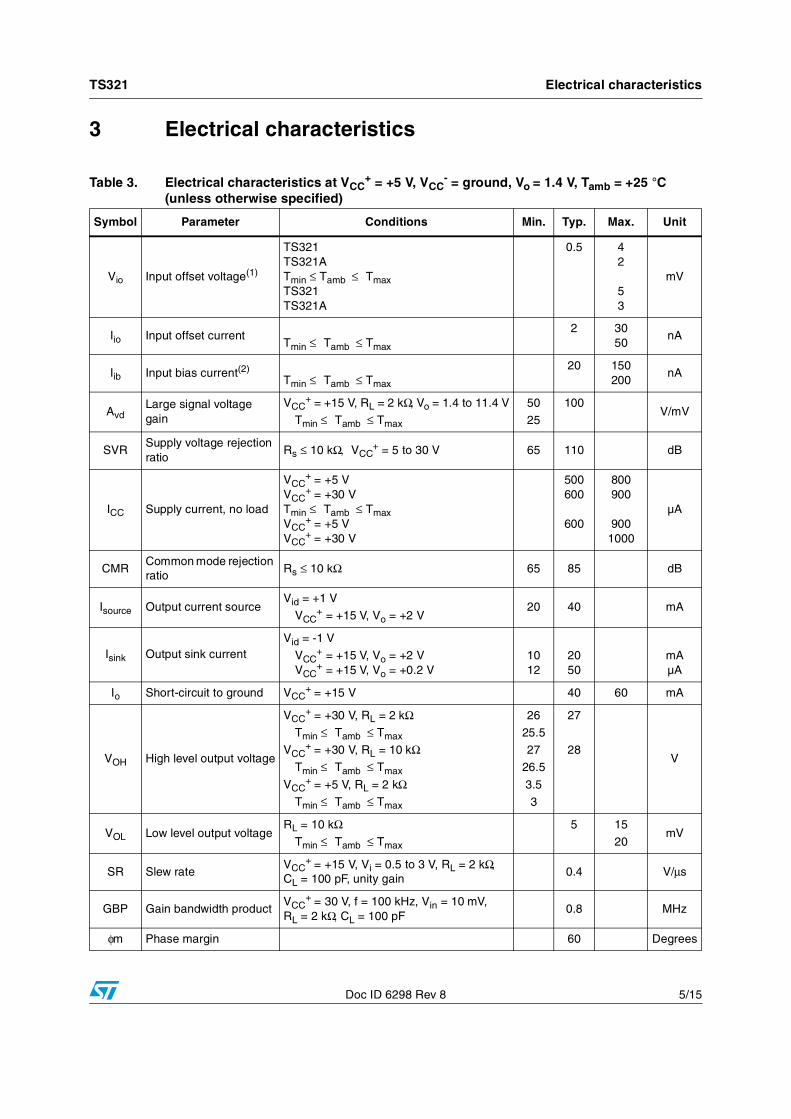
TS321 Electrical characteristics
Doc ID 6298 Rev 8 5/15
3 Electrical characteristics
Table 3. Electrical characteristics at VCC+ = +5 V, VCC
- = ground, Vo = 1.4 V, Tamb = +25 °C (unless otherwise specified)
Symbol Parameter Conditions Min. Typ. Max. Unit
Vio Input offset voltage(1)
TS321 TS321A Tmin ≤ Tamb ≤ Tmax TS321TS321A
0.5 42
53
mV
Iio Input offset currentTmin ≤ Tamb ≤ Tmax
2 3050
nA
Iib Input bias current(2)Tmin ≤ Tamb ≤ Tmax
20 150200
nA
AvdLarge signal voltage gain
VCC+ = +15 V, RL = 2 kΩ, Vo = 1.4 to 11.4 V
Tmin ≤ Tamb ≤ Tmax
50
25
100V/mV
SVRSupply voltage rejection ratio
Rs ≤ 10 kΩ, VCC+ = 5 to 30 V 65 110 dB
ICC Supply current, no load
VCC+ = +5 V
VCC+ = +30 V
Tmin ≤ Tamb ≤ TmaxVCC
+ = +5 VVCC
+ = +30 V
500600
600
800900
9001000
µA
CMRCommon mode rejection ratio
Rs ≤ 10 kΩ 65 85 dB
Isource Output current source Vid = +1 V
VCC+ = +15 V, Vo = +2 V
20 40 mA
Isink Output sink currentVid = -1 V
VCC+ = +15 V, Vo = +2 V
VCC+ = +15 V, Vo = +0.2 V
1012
2050
mAµA
Io Short-circuit to ground VCC+ = +15 V 40 60 mA
VOH High level output voltage
VCC+ = +30 V, RL = 2 kΩ
Tmin ≤ Tamb ≤ Tmax
VCC+ = +30 V, RL = 10 kΩ
Tmin ≤ Tamb ≤ Tmax
VCC+ = +5 V, RL = 2 kΩ
Tmin ≤ Tamb ≤ Tmax
26
25.5
27
26.5
3.5
3
27
28V
VOL Low level output voltageRL = 10 kΩ
Tmin ≤ Tamb ≤ Tmax
5 15
20mV
SR Slew rate VCC
+ = +15 V, Vi = 0.5 to 3 V, RL = 2 kΩ, CL = 100 pF, unity gain
0.4 V/μs
GBP Gain bandwidth product VCC
+ = 30 V, f = 100 kHz, Vin = 10 mV,RL = 2 kΩ, CL = 100 pF
0.8 MHz
φm Phase margin 60 Degrees

Electrical characteristics TS321
6/15 Doc ID 6298 Rev 8
THD Total harmonic distortionf = 1 kHz, AV = 20 dB, RL = 2 kΩ, Vo = 2 Vpp, CL = 100 pF, VCC
+ = +30 V0.015 %
enEquivalent input noise voltage
f = 1 kHz, Rs = 100 Ω, VCC+ = +30 V 40
1. Vo = 1.4 V, Rs = 0 Ω, 5 V < VCC+ < 30 V, 0 < Vicm < VCC
+ - 1.5 V.
2. The direction of the input current is out of the IC. This current is essentially constant and independent of the state of the output, therefore there is no change in the load on the input lines.
Table 3. Electrical characteristics at VCC+ = +5 V, VCC
- = ground, Vo = 1.4 V, Tamb = +25 °C (unless otherwise specified) (continued)
Symbol Parameter Conditions Min. Typ. Max. Unit
nV
Hz------------

TS321 Electrical characteristics
Doc ID 6298 Rev 8 7/15
Figure 2. Current consumption versus temperature
Figure 3. AC-coupled inverting amplifier
Figure 4. Non-inverting DC gain Figure 5. AC-coupled non-inverting amplifier
Figure 6. DC summing amplifier

Macromodel TS321
8/15 Doc ID 6298 Rev 8
4 Macromodel
4.1 Important note concerning this macromodelNote the following remarks before using the macromodel.
● All models are a trade-off between accuracy and complexity (that is, simulation time).
● Macromodels are not a substitute to breadboarding; rather, they confirm the validity of a design approach and help to select surrounding component values.
● A macromodel emulates the nominal performance of a typical device within specified operating conditions (temperature, supply voltage, for example). Thus the macromodel is often not as exhaustive as the datasheet, its purpose is to illustrate the main parameters of the product.
Data derived from macromodels used outside of the specified conditions (VCC, temperature, for example) or even worse, outside of the device’s operating conditions (VCC, Vicm, for example), is not reliable in any way.
4.2 Macromodel code** Standard Linear Ics Macromodels, 1993.
** CONNECTIONS :
* 1 INVERTING INPUT
* 2 NON-INVERTING INPUT
* 3 OUTPUT
* 4 POSITIVE POWER SUPPLY
* 5 NEGATIVE POWER SUPPLY
.SUBCKT TS321 1 2 3 4 5
***************************
.MODEL MDTH D IS=1E-8 KF=3.104131E-15 CJO=10F
* INPUT STAGE
CIP 2 5 1.000000E-12
CIN 1 5 1.000000E-12
EIP 10 5 2 5 1
EIN 16 5 1 5 1
RIP 10 11 2.600000E+01
RIN 15 16 2.600000E+01
RIS 11 15 2.003862E+02
DIP 11 12 MDTH 400E-12
DIN 15 14 MDTH 400E-12
VOFP 12 13 DC 0
VOFN 13 14 DC 0
IPOL 13 5 1.000000E-05
CPS 11 15 3.783376E-09
DINN 17 13 MDTH 400E-12
VIN 17 5 0.000000e+00
DINR 15 18 MDTH 400E-12
TS321 Macromodel
Doc ID 6298 Rev 8 9/15
VIP 4 18 2.000000E+00
FCP 4 5 VOFP 3.400000E+01
FCN 5 4 VOFN 3.400000E+01
FIBP 2 5 VOFN 2.000000E-03
FIBN 5 1 VOFP 2.000000E-03
* AMPLIFYING STAGE
FIP 5 19 VOFP 3.600000E+02
FIN 5 19 VOFN 3.600000E+02
RG1 19 5 3.652997E+06
RG2 19 4 3.652997E+06
CC 19 5 6.000000E-09
DOPM 19 22 MDTH 400E-12
DONM 21 19 MDTH 400E-12
HOPM 22 28 VOUT 7.500000E+03
VIPM 28 4 1.500000E+02
HONM 21 27 VOUT 7.500000E+03
VINM 5 27 1.500000E+02
EOUT 26 23 19 5 1
VOUT 23 5 0
ROUT 26 3 20
COUT 3 5 1.000000E-12
DOP 19 25 MDTH 400E-12
VOP 4 25 2.242230E+00
DON 24 19 MDTH 400E-12
VON 24 5 7.922301E-01
.ENDS
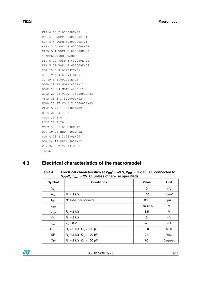
4.3 Electrical characteristics of the macromodel
Table 4. Electrical characteristics at VCC+ = +3 V, VCC
- = 0 V, RL, CL connected to VCC/2, Tamb = 25 °C (unless otherwise specified)
Symbol Conditions Value Unit
Vio 0 mV
Avd RL = 2 kΩ 100 V/mV
ICC No load, per operator 300 µA
Vicm 0 to +3.5 V
VOH RL = 2 kΩ 3.5 V
VOL RL = 2 kΩ 5 mV
Ios Vo = 0 V 40 mA
GBP RL = 2 kΩ, CL = 100 pF 0.8 MHz
SR RL = 2 kΩ, CL = 100 pF 0.4 V/μs
∅m RL = 2 kΩ, CL = 100 pF 60 Degrees
Package information TS321
10/15 Doc ID 6298 Rev 8
5 Package information
In order to meet environmental requirements, ST offers these devices in different grades of ECOPACK® packages, depending on their level of environmental compliance. ECOPACK specifications, grade definitions and product status are available at: www.st.com. ECOPACK is an ST trademark.
TS321 Package information
Doc ID 6298 Rev 8 11/15
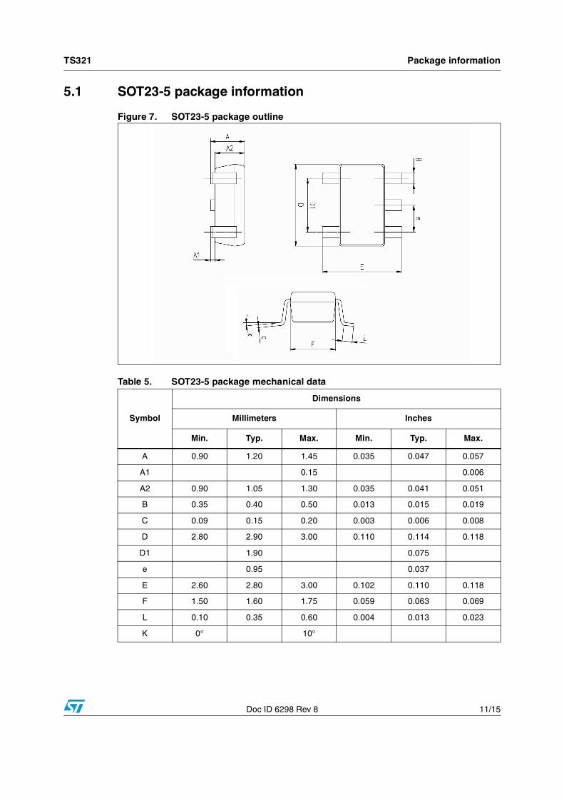
5.1 SOT23-5 package information
Figure 7. SOT23-5 package outline
Table 5. SOT23-5 package mechanical data
Symbol
Dimensions
Millimeters Inches
Min. Typ. Max. Min. Typ. Max.
A 0.90 1.20 1.45 0.035 0.047 0.057
A1 0.15 0.006
A2 0.90 1.05 1.30 0.035 0.041 0.051
B 0.35 0.40 0.50 0.013 0.015 0.019
C 0.09 0.15 0.20 0.003 0.006 0.008
D 2.80 2.90 3.00 0.110 0.114 0.118
D1 1.90 0.075
e 0.95 0.037
E 2.60 2.80 3.00 0.102 0.110 0.118
F 1.50 1.60 1.75 0.059 0.063 0.069
L 0.10 0.35 0.60 0.004 0.013 0.023
K 0° 10°

Package information TS321
12/15 Doc ID 6298 Rev 8
5.2 SO-8 package information
Figure 8. SO-8 package outline
Table 6. SO-8 package mechanical data
Symbol
Dimensions
Millimeters Inches
Min. Typ. Max. Min. Typ. Max.
A 1.75 0.069
A1 0.10 0.25 0.004 0.010
A2 1.25 0.049
b 0.28 0.48 0.011 0.019
c 0.17 0.23 0.007 0.010
D 4.80 4.90 5.00 0.189 0.193 0.197
H 5.80 6.00 6.20 0.228 0.236 0.244
E1 3.80 3.90 4.00 0.150 0.154 0.157
e 1.27 0.050
h 0.25 0.50 0.010 0.020
L 0.40 1.27 0.016 0.050
L1
k 0° 8° 1° 8°
ccc 0.10 0.004

TS321 Ordering information
Doc ID 6298 Rev 8 13/15
6 Ordering information
Table 7. Order codes
Part numberTemperature
rangePackage Packaging Marking
TS321ILT
-40 °C, +125 °C
SOT23-5L Tape and reelK401
TS321AILT K402
TS321ID/IDTSO-8
Tube ortape and reel
321I
TS321AID/AIDT 321AI
TS321IYLT(1)
1. Qualified and characterized according to AEC Q100 and Q003 or equivalent, advanced screening according to AEC Q001 and Q 002 or equivalent.
SOT23-5L(automotive grade level)
Tape and reelK406
TS321AIYLT(1) K407

Revision history TS321
14/15 Doc ID 6298 Rev 8
7 Revision history
Table 8. Document revision history
Date Revision Changes
30-Jun-2001 1 Initial release.
04-Jul-2005 2PPAP references inserted in the datasheet, see order codes table.
ESD protection inserted in Table 1: Absolute maximum ratings.
06-Sep-2005 3Correction of errors in package names and markings in order codes table.
Minor grammatical and formatting corrections.
12-Dec-2005 4
Missing PPAP references inserted, see order codes table.
Thermal resistance junction to ambient and thermal resistance junction to case information added in Table 1: Absolute maximum ratings.
Macromodel updated see Section 4: Macromodel.
08-Nov-2007 5
Added CDM value for SO-8 in Table 1: Absolute maximum ratings.
Added Tj value in Table 1: Absolute maximum ratings.
Macromodel updated see Section 4: Macromodel.
Reformatted package information.
Added footnote in Table 7: Order codes.
Removed TS321IYD/IYDT and TS321AIYD/AIYDT order codes.
08-Jul-2008 6Added CDM value for SOT23-5 package in Table 1: Absolute maximum ratings.
10-May-2010 7 Updated package information in Chapter 5.
12-Sep-2012 8Qualified status of TS321IYLT and TS321AIYLT order codes in Table 7, minor corrections throughout document.

TS321
Doc ID 6298 Rev 8 15/15
Please Read Carefully:
Information in this document is provided solely in connection with ST products. STMicroelectronics NV and its subsidiaries (“ST”) reserve theright to make changes, corrections, modifications or improvements, to this document, and the products and services described herein at anytime, without notice.
All ST products are sold pursuant to ST’s terms and conditions of sale.
Purchasers are solely responsible for the choice, selection and use of the ST products and services described herein, and ST assumes noliability whatsoever relating to the choice, selection or use of the ST products and services described herein.
No license, express or implied, by estoppel or otherwise, to any intellectual property rights is granted under this document. If any part of thisdocument refers to any third party products or services it shall not be deemed a license grant by ST for the use of such third party productsor services, or any intellectual property contained therein or considered as a warranty covering the use in any manner whatsoever of suchthird party products or services or any intellectual property contained therein.
UNLESS OTHERWISE SET FORTH IN ST’S TERMS AND CONDITIONS OF SALE ST DISCLAIMS ANY EXPRESS OR IMPLIEDWARRANTY WITH RESPECT TO THE USE AND/OR SALE OF ST PRODUCTS INCLUDING WITHOUT LIMITATION IMPLIEDWARRANTIES OF MERCHANTABILITY, FITNESS FOR A PARTICULAR PURPOSE (AND THEIR EQUIVALENTS UNDER THE LAWSOF ANY JURISDICTION), OR INFRINGEMENT OF ANY PATENT, COPYRIGHT OR OTHER INTELLECTUAL PROPERTY RIGHT.
UNLESS EXPRESSLY APPROVED IN WRITING BY TWO AUTHORIZED ST REPRESENTATIVES, ST PRODUCTS ARE NOTRECOMMENDED, AUTHORIZED OR WARRANTED FOR USE IN MILITARY, AIR CRAFT, SPACE, LIFE SAVING, OR LIFE SUSTAININGAPPLICATIONS, NOR IN PRODUCTS OR SYSTEMS WHERE FAILURE OR MALFUNCTION MAY RESULT IN PERSONAL INJURY,DEATH, OR SEVERE PROPERTY OR ENVIRONMENTAL DAMAGE. ST PRODUCTS WHICH ARE NOT SPECIFIED AS "AUTOMOTIVEGRADE" MAY ONLY BE USED IN AUTOMOTIVE APPLICATIONS AT USER’S OWN RISK.
Resale of ST products with provisions different from the statements and/or technical features set forth in this document shall immediately voidany warranty granted by ST for the ST product or service described herein and shall not create or extend in any manner whatsoever, anyliability of ST.
ST and the ST logo are trademarks or registered trademarks of ST in various countries.
Information in this document supersedes and replaces all information previously supplied.
The ST logo is a registered trademark of STMicroelectronics. All other names are the property of their respective owners.
© 2012 STMicroelectronics - All rights reserved
STMicroelectronics group of companies
Australia - Belgium - Brazil - Canada - China - Czech Republic - Finland - France - Germany - Hong Kong - India - Israel - Italy - Japan - Malaysia - Malta - Morocco - Philippines - Singapore - Spain - Sweden - Switzerland - United Kingdom - United States of America
www.st.com