low-volume pfc rectifier based on non-symmetric …
TRANSCRIPT

0885-8993 (c) 2013 IEEE. Translations and content mining are permitted for academic research only. Personal use is also permitted, but republication/redistribution requires IEEEpermission. See http://www.ieee.org/publications_standards/publications/rights/index.html for more information.
This article has been accepted for publication in a future issue of this journal, but has not been fully edited. Content may change prior to final publication. Citation information: DOI10.1109/TPEL.2014.2317723, IEEE Transactions on Power Electronics
1
LOW-VOLUME PFC RECTIFIER BASED ON NON-SYMMETRIC MULTI-LEVEL BOOST CONVERTER
Behzad Mahdavikhah and Aleksandar Prodić
Laboratory for Power Management and Integrated Switch-Mode Power Supplies
ECE Department, University of Toronto
10 King’s College Road, Toronto, ON, M5S 3G4, CANADA
E-mail: {bmehrabad, prodic}@ece.utoronto.ca
Abstract— This paper introduces a digitally controlled single-phase rectifier with power factor correction (PFC)
based on a modified three-level boost converter topology. In comparison with the conventional boost based systems,
the new PFC rectifier has about three times smaller inductor and significantly lower switching losses. The
improvements are achieved by replacing the output capacitor of the boost converter with a non-symmetric active
capacitive divider, with a 3:1 division ratio, and by utilizing the downstream converter stage for the capacitive
divider’s centre tap voltage regulation. The non-symmetric voltage divider and applied switching sequence
effectively provide four-level converter behavior using the same number of components as three-level converters. As
a result a 66% reduction of the inductor compared to the conventional boost based PFC and a 33% compared to the
standard three-level solutions operating at the same effective switching frequencies are also achieved.
Experimental results obtained with a 350 W, 200 kHz, universal input voltage (85Vrms - 265Vrms) PFC prototype
demonstrate three times smaller inductor current ripple than that of the conventional boost converter allowing for the
same inductor reduction. Efficiency improvements of up to a 6% are also demonstrated.
Note: A portion of this work was presented at the IEEE APEC 2013 Conference and Exhibition.
Corresponding Author: Address:
Prof. Aleksandar Prodić University of Toronto, ECE Department
Email: [email protected] 10 King’s College Road
Phone: (416) 946-0227 Toronto, ON, M5S 3G4, CANADA
I. INTRODUCTION
The boost converter operating in continuous current mode (CCM) followed by an isolated dc-dc converter [1], [2] is
among the most widely used configurations in single-phase rectifiers with power factor correction (PFC). This is
mostly due to the continuous input current of the boost stage reducing electromagnetic interference (EMI) filtering
requirements and fairly simple controller implementation [2-5]. This topology is used in a wide range of applications
requiring between 100W and 500W of power. Some examples include laptop and personal computers, monitors,
communication equipment, TV sets and other consumer electronics.
One of the major drawbacks of the boost-based front stage is a relatively large size of the inductor limiting its use in
weight and volume sensitive applications. The large inductor also causes non-negligible core losses [5], [6] and
results in a relatively large parasitic capacitance of the winding introducing high frequency noise [7]. The
conventional boost-based topologies also suffer from problems related to switching losses [2], [8], causing heat
dissipation, whose handling often requires bulky cooling components. The switching losses are mostly related to the

0885-8993 (c) 2013 IEEE. Translations and content mining are permitted for academic research only. Personal use is also permitted, but republication/redistribution requires IEEEpermission. See http://www.ieee.org/publications_standards/publications/rights/index.html for more information.
This article has been accepted for publication in a future issue of this journal, but has not been fully edited. Content may change prior to final publication. Citation information: DOI10.1109/TPEL.2014.2317723, IEEE Transactions on Power Electronics
2
operation of the transistor and the diode at the relatively high output, i.e. bus, voltage, which for the universal input
(85 Vrms to 265 Vrms) boost PFCs it is usually about 400 V.
To minimize the size of the boost-based PFC system inductors, a number of methods have been proposed in the past
[5-15]. Those can generally be divided into frequency-increase based and topological changes.
Interleaved topologies [13-15], which reduce the inductor by effectively increasing the switching frequency, have
proven to be effective solutions for larger power ratings, where the semiconductor switching components can be
fully utilized. However, these solutions still suffer from relatively high switching losses and, when operating at light
and medium loads, from either degradation of efficiency or quality of the input current waveform [16].
The topological methods [5-11], minimize both the inductor value and the switching losses, by reducing the stress of
the components. In the flying capacitor multi-cell boost [7], derived from the multilevel concepts [12], these
advantages are achieved by adding few switches and a relatively large flying capacitor. A three-level boost-based
PFC [6] replaces the output capacitor of the boost converter with a compact active capacitive divider and, for the
same switching frequency, results in a 50% reduction of the inductor value compared to the conventional boost-
based solutions.
The main goal of this paper is to introduce a novel single-phase multi-level boost based PFC rectifier that allows
further reduction of the inductor volume while maintaining the benefits of the previously presented multi-level
solutions. The new converter, named non-symmetric multi-level boost (NSMB), and its digital controller are shown
in Fig.1. The new converter and its controller are primarily designed for the previously mentioned applications
ranging between 100 W and 500W. The new topology reduces the size of the boost inductor to a one third of the
value required for the conventional boost PFC using the same number and volume of components as the 3-level
flying-capacitor-less divider based solution [6]. In essence, utilizing similar hardware as a three level converter, the
introduced topology operates as a four level converter. This results in the improvements similar to those obtained by
moving from a conventional 2-level boost to a 3-level topology without increasing hardware complexity. Like other
multi-level solutions the NSMB also reduces the switching losses and components voltage stress. The new topology
is also well suited to be used with efficiency optimization methods and techniques developed for conventional boost
based topologies [17]-[21], allowing all advantages of the previously developed methods to be utilized here as well.
The inductor reduction is achieved by providing non-equal voltages across the capacitive divider cells, through a
capacitor divider with a 3:1 conversion ratio, and applying a switching scheme that results in four inductor voltage
levels. Compared to the conventionally used four-level boost solutions [7], [12], the NSMB has the same inductor
volume when operating at the same switching frequency. Still, the new converter requires a smaller number of
switching components and eliminates the bulky flying capacitor for the regulation of the voltages of the divider taps.
Liin(t)
C
2C
+
vout(t)
_
Q1
Q2
D2
+
2Vbus/3
_
+
_
D1
Signal comparators and
mode selector
Dual-input isolated dc-dc
downstream converter
H
vx(t)
+
vin(t)
_Full-wave diode
rectifier
vline(t)
+
_ Vbus/3
H
Load
vct(t)
vtop(t)
cd(t)
Hdvout(t)
H Hd
Input current and buss voltage regulator
Downstream stage
controller
Averaged current programmed mode
controller
Centre-tap voltage
regulator
Pulse redirection
logic
Hvtop(t)
Hvct(t)
d[n]Hvin(t)
cd1(t) cd2(t)c1(t) c2(t)
NSMB Controller
Rsiin(t) Hvin(t) Hvct(t) Hvtop(t)
c1(t)
c2(t)
Fig. 1: Non-symmetric multi-level boost (NSMB) based PFC rectifier and its downstream stage.

0885-8993 (c) 2013 IEEE. Translations and content mining are permitted for academic research only. Personal use is also permitted, but republication/redistribution requires IEEEpermission. See http://www.ieee.org/publications_standards/publications/rights/index.html for more information.
This article has been accepted for publication in a future issue of this journal, but has not been fully edited. Content may change prior to final publication. Citation information: DOI10.1109/TPEL.2014.2317723, IEEE Transactions on Power Electronics
3
In this case, as shown in Fig.1, the capacitive divider voltages are regulated with the downstream dc-dc converter
that, compared to traditional solutions, also has smaller volume and better efficiency, due to reduced voltage swing
across its components.
The controller for the NSMB PFC of Fig.1 consists of two blocks, input current and bus voltage regulator and the
centre-tap voltage regulator. The first block, regulates the input current iin(t) and the intermediate bus voltage Vbus,
i.e. the output voltage of the first stage. This block is a modification of the digital average current programmed mode
solution presented in [22]. The second block regulates the centre tap voltage of the capacitive divider vct(t) such that
the divider attenuation ratio of 3:1 is constantly maintained. This regulation is performed by steering the input
currents of a dual-input downstream stage and, in that way regulating the discharging of the two capacitors. This
block is designed to operate in synchronization with any dedicated constant frequency controller of the downstream
stage producing a pulse width modulated signal cd(t).
This paper is organized as follows: The following section explains the principle of NSMB converter operation. In
Section III challenges related to the control of the NSMB-based PFC rectifier are addressed and a practical digital
control based solution is presented. Section IV shows experimental results that verify advantages of the NSMB-
based converter over conventional solutions.
II. PRINCIPLE OF OPERATION OF THE NON-SYMMETRIC MULTI-LEVEL BOOST-BASED (NSMB) FRONT END PFC STAGE
To minimize the inductor volume, the introduced non-symmetric multi-level boost (NSMB) converter of Fig. 1
operates on the same fundamental principles as other multi-level solutions. It utilizes the fact that by reducing the
voltage swing across the boost inductor the inductance value can be reduced as well.
The relation between the inductance value L and the maximum voltage swing of the inductor can be described with the
help of the circuit and timing diagrams shown in Fig.2.a. The figures demonstrate variation of the inductor voltage in a
general boost-based converter operating with constant output voltage. In the presented equivalent circuit vx_on(t) and
vx_off(t) are the values of the switching node voltage during the inductor charging and discharging phase, respectively.
Figure 2.b shows that for the conventional boost the two values are equal to vx_on(t) = 0 and vx_off(t) = Vbus.
The analysis starts from the expressions for the inductor current ripple for a general boost-based converter:
I r ipplevL _high(t)
2L
D
fswvin (t) vx_on
2L
D
fsw (1)
Ir ipplevL_ low(t)
2L
D'
fswvin (t) vx_off
2L
D'
fsw
, (2)
_
Liin(t)
Vx_on
+vin(t)
_
+
vx(t)
+
_vL(t) +
_
vL
vx
0 d(t)Ts
Vx_off
vin(t)-vx_off
vin(t)-vx_on
b)a)
Vx_off
+
_
SW1
SW2
Vx_on
t
t
Vswing
Vswing
Liin(t)
vin(t)
_
+
vx(t)
+
_vL(t)
_
SW1
SW2
vL
vx
0 d(t)Ts
Vbuss
vin(t)-Vbuss
vin(t)
0
t
t
Vswing
Vswing
CVbus
_
+ +
Ts Ts
SW1 - on
SW1 - on SW2 - onSW2 - on
loa
d
Fig. 2: Equivalent circuit for the analysis of the inductor voltage swing and the voltage waveforms of (a) a general boost-based
converter and (b) the conventional boost.

0885-8993 (c) 2013 IEEE. Translations and content mining are permitted for academic research only. Personal use is also permitted, but republication/redistribution requires IEEEpermission. See http://www.ieee.org/publications_standards/publications/rights/index.html for more information.
This article has been accepted for publication in a future issue of this journal, but has not been fully edited. Content may change prior to final publication. Citation information: DOI10.1109/TPEL.2014.2317723, IEEE Transactions on Power Electronics
4
where, vL_high(t) and vL_low(t) are the high and the low values of the inductor voltage during one switching cycle,
respectively, vin(t) is the input voltage, fsw is the switching frequency of the converter, and D is the duty ratio.
The maximum ripple, occurring for D = 0.5 [6], can be described with the following expression, obtained by
combining (1) and (2):
I ripple_max vL _high(t) vL _ low(t)
8L1
fswVswing_L
8L
1
fswVswing_ x
8L
1
fsw , (3)
where Vswing_L and Vswing_x are the voltage swings of the inductor and switching node, respectively. It can be seen that
the ripple, which determines the inductance value [23], is linearly proportional to the voltage swing across the
switching node. The relation also shows that, for the boost based converters, the inductor voltage swing is equal to the
switching node swing and by minimizing that value, the inductor can be reduced without affecting the current ripple
amplitude.
This analysis shows that for the conventional boost the switching node voltage swing is equal to its output voltage. In
typical PFC rectifiers, this voltage, labeled as Vbus in Fig 2.b, is fairly high, usually around 400 V, causing the
inductor value and the switching losses to be relatively large. In the applications of interest, the switching losses
usually have a large influence on the overall power processing efficiency of the converter [5], [6], [24]. The losses
also indirectly increase the overall system volume, by imposing additional cooling requirements for the
semiconductor components.
To minimize the swing and, therefore, reduce both the inductor value and switching losses, in the NSMB converter
of Fig.1, an active capacitive divider with 3:1 conversion ratio replaces the output capacitor and switches of the
conventional boost. This allows the switching node voltage to be changed between four possible values: 0, Vbus/3,
2Vbus/3, and Vbus, effectively creating a 4-level structure using a 3-level configuration. The divider and its switching
sequence are designed to allow vx_on(t) and vx_off(t) to be dynamically changed as the input voltage changes, such that
the inductor voltage swing is limited to Vbus/3. This value is three times lower than that of a conventional boost and
33% smaller than the voltage swing of the 3-level topologies [6], [7] operating at the same effective switching
frequency. As a result equal reductions of the inductor are allowed and large efficiency improvements obtained. It
should be noted that similar to the solution presented in [6] it would be possible to operate the NSMB at the twice
switching frequency of the conventional boost while maintaining the same power processing efficiency. Such an
operation would result in a 6 times smaller inductor volume compared to that of the conventional boost, but would
significantly increase power dissipation per unit volume potentially resulting in increased cooling requirements and
reliability problems. For that reason, throughout the paper comparison was performed with the assumption that the
topologies operate at the same effective switching frequency and simultaneous improvements in power processing
efficiency and volume reduction are targeted.
A. Non-symmetric active capacitive divider
The operation of the non-symmetric capacitive divider can be explained by looking at the rectified line input voltage
and diagrams of Figs. 3 to 5. The diagrams describe three distinctive modes of converter operation, which depend on
the instantaneous value of the rectified line voltage vin(t) = |vline(t)| (Fig.1).
Mode 1: for vin(t) < Vbus/3 the converter operates in mode 1, depicted with the diagrams of Fig.3. Throughout this
mode, switch SW1 is kept on, reverse biasing the diode D1, and the other two switches (SW2 and D2) are active,
operating at the switching rate fsw = 1/Tsw. The on-time of SW2, i.e. duty ratio, is regulated by the controller of Fig.1.
vin(t)
Vbus/3
2Vbus/3
0
a)
Tline/2
2C
Liin(t)
Q2
D1
D2
C
+
_
+
_Vbus/3
2Vbus/3
Discharge
vin(t)
_
+
vx(t)=Vbus/3Liin(t)
Q2
D1
D2
C
+
_
+
_Vbus/3
2Vbus/3
Charge
vin(t)
_
+
vx(t)=0
2C
b) c)
Q1 Q1
Mode 1
Fig. 3: Mode 1 of operation of the non-symmetric multi-level boost front-end stage: a) input voltage range for mode 1; b)
equivalent circuit of the converter during inductor charging phase; c) equivalent circuit during the discharging.

0885-8993 (c) 2013 IEEE. Translations and content mining are permitted for academic research only. Personal use is also permitted, but republication/redistribution requires IEEEpermission. See http://www.ieee.org/publications_standards/publications/rights/index.html for more information.
This article has been accepted for publication in a future issue of this journal, but has not been fully edited. Content may change prior to final publication. Citation information: DOI10.1109/TPEL.2014.2317723, IEEE Transactions on Power Electronics
5
The current conducting paths for the both portions of a switching period are shown in Fig. 3 with bold red lines, where
Fig.3.a corresponds to the inductor charging process, i.e. on-time of SW2, and Fig.3.b shows its discharging.
It can be seen that during the on-state of SW2, vx(t) = 0 and during its off state vx(t)=Vbus/3. Therefore, the maximum
voltage swing across the inductor is Vbus/3 equal to the voltage of the divider bottom capacitor. It should be noted in
this mode both SW2 and D2 operate at Vbus/3 and the switching losses are lower than those of the conventional boost
and 3-level boost, which switches operate at Vbus and Vbus/2, respectively
This mode is maintained as long as vin(t) is lower than Vbus/3 and the condition for the regular boost operation, i.e. the
bottom capacitor voltage is larger than the input voltage, satisfied.
Mode 2 of operation, shown in Fig.4, occurs for Vbus/3 < vin(t) < 2Vbus/3. In this mode, during the first portion of a
switching period, corresponding to the transistor on-state in the conventional topology, SW1 and D2 are turned on and
the switching node voltage is Vbus/3 as it can be seen from Fig.4.a). During the remaining portion of the switching
period, SW2 and D1 are conducting and, as shown in Fig.4.b), the switching node voltage is 2Vbus/3. It can be seen
that, in this way, the absolute value of the voltage swing is again limited to Vbus/3.
In this mode, the switching losses are approximately the same as those of the conventional boost (and 3-level boost),
since the total blocking voltage of the two switches operating in the each portion of a switching interval is equal to
that of the conventional boost.
Mode 3, shown in Fig.5, is activated when vin(t) exceeds 2Vbus/3. Throughout this mode the transistor SW1 is turned
off allowing diode D1 to conduct. In this mode, during the first portion of the switching interval, SW2 is conducting
and the voltage across the switching node is 2Vbus/3 as shown in Fig.5.a). During the second portion of the interval,
D2 conducts and the switching node voltage is Vbus. Again, the inductor voltage swing is limited to Vbus/3.
In this mode the switching losses are again lower than that of the conventional boost and of the 3-level boost, since
both SW2 and the D2 interrupt only one third of the converter output voltage.
L
Q1
Q2
D1
D2
+
_
+
_
vin(t)
0
vin(t)
_
+
Tline/2
Vbus/3
C
2C
2Vbus/3
2Vbus/3
Vbus/3
L
Q1
Q2
D1
D2
+
_
+
_
vin(t)
_
+
vx(t)=2Vbus/3
Vbus/3
C
2C
2Vbus/3
DischargeCharge
vx(t)=Vbus/3iin(t)iin(t)
b)a) c)
Mode 2
Fig. 4: Mode 2 of operation of the NSMB front-end stage: a) input voltage range for mode 2; b) equivalent circuit of the converter
during inductor charging phase; c) equivalent circuit during the discharging.
Since, as mentioned earlier, in the applications of interest the switching losses are dominant, an analysis of
conduction losses for the NSMB is given in Appendix A. It is shown that the conduction losses depend on the input
voltage amplitude and the amounts of time NSMB spends in each of the three modes. The analysis also shows that,
for an optimally designed NSMB, with switches D1, SW1 rated at 2Vbus/3 and SW2, D2 rated at Vbus/3, the conduction
losses are approximately the same as those of the conventional boost.
L
Q1
Q2
D1
+
_
+
_
D2
vin(t)
0
vin(t)
_
+
Mode 3
Tline/2
vx(t)=2Vbus/3
2C
2Vbus/3
Vbus/3
2Vbus/3
Vbus/3
L
Q1
Q2
D1
+
_
+
_
D2
vin(t)
_
+
vx(t)=Vbus
C
2C
2Vbus/3
Vbus/3
DischargeChargeiin(t)iin(t)
b)a) c)
C
Fig. 5: Mode 3 of operation of the NSMB front-end stage: a) input voltage range for mode 3; b) equivalent circuit of the converter
during inductor charging phase; c) equivalent circuit during the discharging.

0885-8993 (c) 2013 IEEE. Translations and content mining are permitted for academic research only. Personal use is also permitted, but republication/redistribution requires IEEEpermission. See http://www.ieee.org/publications_standards/publications/rights/index.html for more information.
This article has been accepted for publication in a future issue of this journal, but has not been fully edited. Content may change prior to final publication. Citation information: DOI10.1109/TPEL.2014.2317723, IEEE Transactions on Power Electronics
6
A.1. Volume Reduction
A.1.1 Inductor Volume
As shown in the theoretical analysis of Section II, the NSMB converter reduces the inductor value by three times
compared to the conventional boost while retaining the same peak inductor current.
Since the inductor volume is proportional to its energy storage capacity [25], [26]:
WE_L 1
2LIpeak
2, (4)
where Ipeak is the peak inductor, it can be concluded that the inductor volume of the NSMB is three times smaller as
well.
It should be noted that compared to the practical two-phase boost interleaved PFC solutions [13], [25], [26] the
inductor of the NSMB is about two times smaller. Even though the inductance value of the interleaved boost is
reduced by four times, compared to the conventional boost the volume reduction is much smaller. As described in
[25], [26], the actually achievable volume reduction is around a 32%, due to the higher inductor current ripple and,
therefore, a larger peak current.
A.1.2. Output capacitor volume
In the NSMB converter, the output capacitor of the conventional boost with a value of Cout, rated at Vout, is replaced
with Cout1 = 3Cout/2, rated at 2Vout/3 and Cout2 = 3Cout, rated at Vout/3. The output capacitance of the boost PFC is
chosen to meet desired hold-up time energy requirement [27] and the output voltage ripple.
By using the same energy-based criteria to compare the capacitors sizes it can be seen that the NSMB has the same
total capacitor volume as the conventional boost and the 3-level boost, since, ideally, the size of a capacitor is
proportional to its energy storing capacity [28], i.e. to its 1/2CV2 product.
The output voltage ripple is comprised of two components, the high frequency ripple, at the switching frequency, and
the low frequency component at twice the line frequency. In both the conventional boost PFC and the introduced
NSMB the high frequency component is much smaller than the component at the twice line frequency and therefore,
can be neglected in the analysis [23]. The following analysis shows that the dominant low frequency component is
the same for the both topologies.
To find the amplitude of the dominant ripple, we can look at the general case, where an increase of the energy E
creates a voltage difference V across the capacitor C having an initial voltage
V. This voltage difference can be found using the following relation:
)2(2
1)(
2
1)(
2
1 222 VVVCVCVVCE . (5)
For the case when V >> V, which is valid for the systems under investigation, the following approximate
expression for the voltage deviation:
CV
EV
, (6)
can be easily derived from (5).
For a general PFC, the increase of the energy can be calculated by looking at the instantaneous power delivered from
the ac source [23],
)]2cos(1[)( tPtplineloadin
, (7)
which, as shown in Fig.6, has two components, a dc component equal to the load power Pload and an ac component
at twice the line frequency. The ac portion of this input power (Pin_ac(t) shown in Fig.6.b) creates the dominant output
voltage ripple. To calculate the peak-to-peak value of this ripple, the amount of energy stored in the capacitor over a
Tline/4 period (shaded area in the diagram of Fig.6.b) can be calculated as:
line
load
Tt
t
lineload
Tt
t
acinacin
PdttPdttpE
lineline
4/4/
__
0
0
0
0
)]2cos([.)( , (8)
and the output capacitor ripple for a boost PFC found by combining (6) and (8):

0885-8993 (c) 2013 IEEE. Translations and content mining are permitted for academic research only. Personal use is also permitted, but republication/redistribution requires IEEEpermission. See http://www.ieee.org/publications_standards/publications/rights/index.html for more information.
This article has been accepted for publication in a future issue of this journal, but has not been fully edited. Content may change prior to final publication. Citation information: DOI10.1109/TPEL.2014.2317723, IEEE Transactions on Power Electronics
7
outoutline
load
outout
acin
boostoutVC
P
VC
EV
_
_2 . (9)
In the case of the NSMB converter, the energy described with (8) is stored across the two output capacitors Ctop and
Cbottom. The distribution of this energy between capacitors, in general, is not equal and depends on the input voltage
level and the portion of the time the converter is spending in each of the operating modes. However, the total energy
given to the system is the same as in the boost case and can be described with the following expression:
bottomacintopacinacinEEE
_____
, (10)
where Ein_ac_top and Ein_ac_top are the portions of energy stored in the top and bottom capacitors, respectively.
By replacing the values in (6) for the NSMB case, the voltage ripples for the top and bottom capacitors Vtop and
Vbottom, respectively, can be obtained as:
outout
bottomacin
outout
bottomacin
bottomoutbottomout
bottomacin
bottomoutVC
E
VC
E
VC
EV
____
__
__
_)3/)(3(
2
, (11)
outout
topacin
outout
topacin
topouttopout
topacin
topoutVC
E
VC
E
VC
EV
____
__
__
_)3/2)(2/3(
2
, (12)
and, since both of the ripple voltages are in phase, the overall ripple of the NSMB can be found as:
outoutline
load
outout
acin
outout
bottomacintopacin
NSMBout
bottomouttopoutNSMBout
VC
P
VC
E
VC
EEV
VVV
_____
_
___
2
,222
. (13)
A comparison of (9) and (13) reveals that both converters have the same ac output voltage ripple while utilizing same
output capacitance volume.
A.1.3. Input filter volume
To fully assess advantages of the NSMB topology over other solutions, input filter requirements are compared in the
following subsection. It is shown that, due to the lower energy of the input current ripple and noise components, the
NSMB potentially can operate with a smaller input filter than that of the conventional boost and of the standard 3-vel
boost. In here, the topological differences in the analysis of the filter requirements are only taken into account
le
ΔEin_acvout(t)
Pin_ac(t)Pload
Tline/4
Vout
vline(t)iin(t)
pin(t) Tline/2
a)
b)
c)
2ΔVout
t
t
t
t0 t0+Tline/4
0 Tline
Fig.6. Waveforms of the output capacitor voltage of an ideal PFC circuit; instantaneous input power, voltage and current
waveforms (a); decomposition of input power components (b); and output capacitor voltage ripple (c)

0885-8993 (c) 2013 IEEE. Translations and content mining are permitted for academic research only. Personal use is also permitted, but republication/redistribution requires IEEEpermission. See http://www.ieee.org/publications_standards/publications/rights/index.html for more information.
This article has been accepted for publication in a future issue of this journal, but has not been fully edited. Content may change prior to final publication. Citation information: DOI10.1109/TPEL.2014.2317723, IEEE Transactions on Power Electronics
8
and the other parameters, such as, influences of the PCB layout and footprints of the components, which also affect
the filter volume [29], are left to be studied in the future.
A properly designed input filter attenuates the input current ripple and two noise components generated by the
switching action of the power supply. Those are the differential mode (DM) noise and common mode (CM) noise.
The previous analysis shows that, for the same switching frequency and three times smaller inductor, the maximum
amplitude of the inductor current ripple is the same for all three configurations. However, as it will be confirmed in
the experimental results section, in the case of the NSMB the total rms value of the ripple component is smaller than
that of the conventional boost, due to longer periods during which the converter operates with close to zero ripple
during mode transitions.
To analyze the influence of the noise components, the equivalent circuits of Fig.7 can be used. The figure shows the
input filter, which includes the ripple and DM reduction components Cx and LDM and the portion of the filter for CM
reduction, comprising of Cy and LCM.
The differential component of the high frequency noise is formed by the current flowing through the input port of the
converter [29], through a path formed by the stray capacitances of the inductor (labeled as CL1 and CL2). In the case
of the NSMB this stray capacitance is smaller than those of the conventional boost and the 3-level boost, due to the
smaller value of the inductor itself [7]. Therefore, this noise is smaller, as demonstrated in the spectrum
measurement, shown in the experimental section. The lower common mode noise allows for reduction of the
differential mode filter components.
The CM noise is mainly generated by the currents flowing from the switching node to the ground through the
parasitic capacitance created by the heat sinks [29], in Fig.7 labeled as Cp1 to Cp6. The power of that noise, and
therefore the size of the common mode filter, is proportional to the amount of energy stored in those parasitic
capacitances during each switching cycle.
Even though the NSMB (and conventional 3-level boost) have a larger number of parasitic components commutating
between the switching node voltage level and the ground, the energy dissipated in them is smaller. This is mainly due
to a lower voltage swing. Fig. 7 shows that in the boost converter, in each cycle, the heat sink parasitic capacitors of
SW1 and D1 (Cp2 and Cp1) are charged/discharged with a voltage swing equal to Vbus, where the size of each capacitor
is proportional to the switch size and the heat sink area. Therefore, the common mode noise is proportional to the
energy transferred through these two capacitors
L
C1
2C1
SW1
SW2
D2
+
2Vbus/3
_
+
_
D1vx(t)
Vbus/3
iin(t)
vin(t)
_
+Cp3
Cp5Full-wave
diode
rectifier
vline(t)
+
_
Cy1
Cy2
Cx1 Cx2
Input filter
Cp6
Cp4
~~~~
~~
CL2 Cd2
Cs2
Cs3
Cd3
L
C1SW1
+
Vbus
_
D1
vx(t)
iin(t)
vin(t)
_
+ +
_
Cp2
Full-wave
diode
rectifier
vline(t)
+
_
Cy1
Cy2
Cx1 Cx2
Input filter
Cp1
~~~~
CL1 Cd1
Cs1
LDM1
LDM2
LCM
LDM1
LDM2
LCM
Fig. 7: The input filter and parasitic capacitances of the boost PFC circuit (top) and NSMB PFC (bottom) circuits.

0885-8993 (c) 2013 IEEE. Translations and content mining are permitted for academic research only. Personal use is also permitted, but republication/redistribution requires IEEEpermission. See http://www.ieee.org/publications_standards/publications/rights/index.html for more information.
This article has been accepted for publication in a future issue of this journal, but has not been fully edited. Content may change prior to final publication. Citation information: DOI10.1109/TPEL.2014.2317723, IEEE Transactions on Power Electronics
9
.2
1
2
1 2
2
2
1_ buspbuspboostcmVCVCW (14)
In the case of the NSMB converter, the parasitic capacitors Cp1 and Cp2 are replaced by four capacitors, i.e. Cp3 to Cp6
corresponding to SW1, D1, SW2 and D2, respectively (Fig.7). Those capacitors are exposed to a three times smaller
voltage swing and therefore, their total energy is
.18
1
18
1
18
1
18
1 2
6
2
5
2
4
2
3_ buspbusbuspbuspNSMBcmVCVCVCVCW (15)
By comparing (14) and (15) it can be concluded that, for the same capacitance values, i.e. for the case when
Cp3+Cp4+Cp5+Cp6=2*(Cp1+Cp2), the total energy stored in the capacitances causing CM noise is about 2/9 times
smaller for the NSMB case. A similar analysis for the 3-level boost can show that, since its voltage swing is Vbus/2,
the total reduction of the energy compared to the boost with the same capacitances is about ½. In an optimized
design of the NSMB (discussed in the Appendix A), where switching components and heat sinks are smaller, an even
larger improvement in the common mode noise reduction can potentially be achieved.
B. Centre tap voltage blancing and isolated downstream stages
The balancing of the capacitor tap voltages in converter topologies incorporating capacitive voltage dividers is often
performed with relatively large flying capacitors [30], [31] or by redirecting the current of the inductor [6], [12],
[32]. For the introduced NSMB the previously used centre tap voltage regulation method cannot directly be applied,
due to the non-equal voltage sharing.
To regulate the centre tap voltage at Vbus/3 without a flying capacitor, here, the downstream converter, inevitably
existing in practically all systems of interest, is used. The regulation is performed by modifying the technique
presented in [32], where the input current of the downstream portion of a merged switched-capacitor buck converter
regulates the centre-tap voltage of its front end. In this case, a two-input isolated downstream stage is used, as shown
in Fig.8. The centre tap voltage is regulated with the two input currents of the downstream converter, i1(t) and i2(t)
with the help of the centre tap voltage regulator.
Depending on the centre-tap voltage level, the switch-selection logic redirects the pulse-width modulated signal
produced by the dedicated downstream stage controller, cd(t), between the two switches (SWd1 and SWd2). The switches are controlled such that the current (charge) is taken either from the top or from the bottom capacitor only.
When the centre tap voltage is exceeding desired Vbus/3 level more current is taken from the bottom cap and when it
is lower the top cap provides more current.
Vbus/3
2Vbus/3
SWd1
SWd2
Dual-input isolated
dc-dc converter
vout(t)
i1(t)
Downstream stage
controller
cd(t)Centre-tap voltage
regulator
To SWd1 and SWd2
i2(t)
Load
2C
iload(t)
+
_
+
+
_
C
_
vout(t)Vbuss/3
Vbuss
Fig. 8: Block diagram of the centre-tap voltage balancing system based on the downstream converter current steering.

0885-8993 (c) 2013 IEEE. Translations and content mining are permitted for academic research only. Personal use is also permitted, but republication/redistribution requires IEEEpermission. See http://www.ieee.org/publications_standards/publications/rights/index.html for more information.
This article has been accepted for publication in a future issue of this journal, but has not been fully edited. Content may change prior to final publication. Citation information: DOI10.1109/TPEL.2014.2317723, IEEE Transactions on Power Electronics
10
Windowed
ADC1
ev[n]kn/Re[n] Voltage loop
compensator
d[n]
ei[n]
Vref
vi_ref(t)
1-bit
∑Δ
Mode selector &
sampling seq.
generator
cmp1
Level
shifter
Rsiline(t)
Windowed
ADC2
Merged multiplier & D/A
Current loop
compensator
reprogram
Digital logic
c(t)
Hvin(t)
Rsiline,avg
Hvtop(t)
DPWM
Low-pass
filter
cmp2
Hvtop(t)Hvct(t)
Input current and buss voltage regulator
c1(t) c2(t)
in.en.Rf
Cf
sel1
Fig.9: Block diagram of the input current and bus voltage regulator.
III. PRACTICAL CONTROLLER IMPLEMENTATION
The controller of Fig.1 consists of two main blocks: input current and voltage regulator and centre-tap voltage
regulator. This section addresses challenges related to the practical NSMB controller realization and shows a
hardware-effective solution for its implementation.
A. Input current and bus voltage regulator
The controller of Fig.9 is a modified version of the average current programmed mode architecture used for a
conventional boost based PFC [33]. In this modification, a new block, named mode selector and sampling sequence
generator is added and the sampling sequence modified, to accommodate operation
with a larger number of switches and eliminate potential stability problems that will soon be addressed. For the same
reason the current loop compensator is also slightly modified.
The regulation of the input current and the output voltage is performed in a similar manner as in the previous
solutions [33], [34], [35]. Based on the digital equivalent of the bus voltage, error value ev[n] is produced by the
ADC1. Based on this value the voltage loop compensator creates a signal k[n]/Re, which is inversely proportional to
the desired emulated resistance seen at the input of the PFC rectifier [23]. This value is then passed to the 1-bit
sigma-delta modulator that, together with the level shifter and the RC filter creates a structure behaving as a merged
analog multiplier and digital-to-analog converter eliminating the need for a costly digital multiplier [33].
This merged structure produces an analog reference
einrefi
R
nktHvtv
][)()(_
(16)
for the current loop, where, H is the gain of the input voltage attenuator and, as mentioned before, vin(t) is the
rectified input voltage (Fig.1). The created analog value is used as the reference for the current loop. This reference
is then compared to the output of the input current sensor Rsiline(t) and a digital equivalent of the current error signal
ei[n] is created, by the windowed ADC2 [33], [36]. The resulting error is sent to the current loop PI compensator that
produces control signal [33]:

0885-8993 (c) 2013 IEEE. Translations and content mining are permitted for academic research only. Personal use is also permitted, but republication/redistribution requires IEEEpermission. See http://www.ieee.org/publications_standards/publications/rights/index.html for more information.
This article has been accepted for publication in a future issue of this journal, but has not been fully edited. Content may change prior to final publication. Citation information: DOI10.1109/TPEL.2014.2317723, IEEE Transactions on Power Electronics
11
]1[][]1[][ nbenaendnd i (17)
where, d[n] and d[n-1] are the current and previous value of the duty ratio control variable, and the compensator
coefficients a and b are selected following the procedure shown in [36]. The produced d[n] value is the control input
for the digital pulse-width modulator (DPWM) producing pulse width modulated signal c(t).
The produced pulse-width modulated signal c(t) is then passed to the mode selector, which operation is described in
the following subsection.
To eliminate switching noise related problems and at the same time obtain the average value of the inductor current
over one switching cycle, the current is sampled using the techniques described in [38], [39]. Depending on the
instantaneous value of d[n], the current is sampled either at the half of the “on” or at the half of the “off” portion of a
switching interval.
B. Mode selector and sampling sequence generator
The mode selector and sampling sequence generator, whose block diagram is shown in Fig.10, outputs pulse-width
modulated signals c1(t) and c2(t) for controlling the NSMB transistors SW1 and SW2, respectively. During mode
transients the selector also changes stored values of the digital current loop compensator, to provide seamless
transition between different modes. The detection of the mode of operation is performed with the two comparators
(cmp1 and cmp2) and with the start-up logic, shown in Fig.10. The comparators cmp1 and cmp2 monitor the input
voltage and detect the transition points at which the vin(t) = vct(t) =Vbus/3 and vin(t) = vtop(t) = 2Vbus/3. The
compensators also initiate mode transition by sending the signals to the mode transition logic. Based on the state of the
comparators and the previous state of the NSMB power stage the transition logic redirects c(t) to appropriate
transistors. The start-up
detector indicates power up conditon of the converter by observing ev[n] and sends the start signal to the mode
transiton. logic, which provides a gradual rise of the bus voltage upon a power up. The mode transiton logic
is a finite state machine (FSM), which operation is demonstrated with the diagram of Fig.11 and described in the
following subsections.
B.1. Seamless mode transitions
To understand the stability problem and a solution for it we can observe how the required conversion ratio changes in
the conventional boost based PFC and in the NSMB based system. In the conventional boost, to maintain a constant
bus voltage, the conversion ratio changes gradually with changes in the input voltage. On the other side, in the
NSMB the conversation ratio drastically changes with each mode transition. Therefore, the duty ratio value required
for maintaining the inductor volt-second balance and the stable output voltage abruptly changes as well. From a
practical point of view this represents a potential problem, since the delays in the controller reaction could cause
mode transition related stability problems.
reprogram
sel1
ev[n]
Mode Selector and s.s. Generator
c(t)
start
sel2
c1(t)
c2(t)Mode transition logic
Start up
detectorS&H1
Hvin
sel1 S&H2sel2
+_
cmp1
+_
cmp2
Hvct Hvtop
Fig.10: Block diagram of the mode selector and sampling sequence generator.

0885-8993 (c) 2013 IEEE. Translations and content mining are permitted for academic research only. Personal use is also permitted, but republication/redistribution requires IEEEpermission. See http://www.ieee.org/publications_standards/publications/rights/index.html for more information.
This article has been accepted for publication in a future issue of this journal, but has not been fully edited. Content may change prior to final publication. Citation information: DOI10.1109/TPEL.2014.2317723, IEEE Transactions on Power Electronics
12
Mode 1
c1(t) = 1
c2(t) = c(t)
Start = 1
Start = 0
cmp1 = 0
cmp2 = 0
cmp1 = 0
Mode
selection
Start-up
c1(t) = c(t)
c2(t) = c(t)
cmp1 = 1
Mode 2
c1(t) = c(t)
c2(t) = c(t)
cmp1 = 1
cmp2 = 0
PI Reprogram
d[n] = max
d[n-1] = max
Mode 3
c1(t) = 0
c2(t) = c(t)
cmp1 = 1
cmp2 = 1
cmp2 = 1
PI Reprogram
d[n] = 0
d[n-1] = 0
cmp2 = 1PI Reprogram
d[n] = max
d[n-1] = max
PI Reprogram
d[n] = 0
d[n-1] = 0
cmp2 = 0
cmp1 = 1
cmp2 = 0
cmp1 = 0
Fig.11: State flow diagram of the mode selector logic.
For example, it can be seen that at the point where the vin(t) is exceeding Vbus/3 (mode 1 to mode 2 transition) the
required conversion ratio changes from one to infinity, requiring controller to change from 0 to full duty ratio value
in a single switching cycle.
To overcome this problem, after each mode transition, the mode selector immediately reprograms the current and the
previous values of the duty ratio in the digital current loop compensator, i.e. d[n] and d[n-1] of Eq.16. This is
performed through the reprogram signal, shown in Fig.10. The decision about the new duty ratio values is made
based on the recognition that after each mode transition, the new duty ratio will be either zero or one. Since at those
points, the required conversion ratio of NSMB is either one or infinite. Therefore, after each transition point is
detected by the comparators, the mode control logic either sets both d[n] and d[n-1] to 0 or to their maximum value.
The diagram of Fig.10 shows the reprogramming values of the PI compensator for all four mode transitions.
B.2. Sampling sequence
By looking at the operation of the NSMB (Figs. 3 to 5) it can be noticed that for some switching states one of the two
output capacitors does not share the same ground with the rest of the circuit. While from the output load, which is
galvanically isolated from the front end stage, this does not represent a problem, this floating ground affects
measurements of the capacitor tap voltages. To measure the tap voltages without the use of relatively costly
differential amplifiers, sample and hold circuits (S&H) shown in Fig.10 are used, and the sampling of the capacitor
tap voltages is done at particular time instants denoted by signals smp1 and smp2 as shown in the diagram of Fig.12.
The value of the top capacitor voltage is sampled during the on state of Q2 and for the bottom capacitor the data
acquisition is performed during D2 conduction time. The ADC1 (Fig.1) also samples vtop(t) during D2 conduction
time, to obtain the bus voltage value.
B.3. Start up
The bypass diode commonly used to ease start-up and inrush current problems in conventional boost solution [40]
cannot be used with the NSMB and similar multi-level solutions [4], [5], [6], [9]. As shown

0885-8993 (c) 2013 IEEE. Translations and content mining are permitted for academic research only. Personal use is also permitted, but republication/redistribution requires IEEEpermission. See http://www.ieee.org/publications_standards/publications/rights/index.html for more information.
This article has been accepted for publication in a future issue of this journal, but has not been fully edited. Content may change prior to final publication. Citation information: DOI10.1109/TPEL.2014.2317723, IEEE Transactions on Power Electronics
13
c2
smp1
t
t
dTsw
Tsw
tblanking
t
tblanking
tblanking
smp2 tblanking
Fig.12: Waveforms of the sampling sequence generator.
in Fig.13, the bypass diode Ds, [40] would short connect the inductor during the first portion of switching period in
mode 3 (Fig.5.b), when vin(t) > vtop(t).
To eliminate the start up problem, the switching sequence is modified during power up, signaled by the high value of
start signal produced by the detector (Fig. 10). During this mode the NSMB operates as a
conventional boost, such that both transistors, i.e. Q1 and Q2 of Fig.1, are turned on during the first portion of a
switching interval and D1 and D2 are allowed to conduct during the rest of the switching period, as shown in Fig.11.
Such operation delivers equal amounts of charge to the both divider capacitors and, ideally, the desired 2:1
distribution of the bus voltage. Possible voltage variations due to component tolerances are eliminated with the
bleeding resistors [41] Rb forming a 3:1 resistive divider. This mode ends when the capacitors are charged to their
reference values and the start signal becomes low, causing the NSMB to switch to the regular mode of operation
described in Section II and by the diagram of Fig.11.
L
Q1
Q2
D1
+
_
+
_
D2
vin(t)
0
vin(t)
_
+
Mode 3
Tline/2
2C
2Vbus/3
Vbus/3
2Vbus/3
Vbus/3
iin(t)
CFull-wave
rectifier
Dst
vline(t)
+
_
Rb
2Rb
Fig. 13: Problem of utilizing bypass diode in the NSMB topology.
To eliminate inrush current problem a number of previously presented solutions can be used [40], [42-44].
C. Centre-tap voltage regulator
As described in the previous section, the regulation of the capacitor voltages is performed with the input current of
the downstream converter. This process is controlled by the centre-tap voltage regulator that redirects current of the
downstream and in that way, regulates the discharging of the both NSMB capacitors.
The downstream converters that can be used with NSMB have two inputs and also utilize the advantages of reduced
voltage swing to minimize the volume and switching losses. Two of many possible implementations of the
downstream stages include two input non-symmetric flyback [22] and the two-input non-symmetric forward, shown
in Figs.14 and 15, describe the operation of the centre-tap voltage regulator with a non-symmetric forward
converter. The transformer of the forward has two primary

0885-8993 (c) 2013 IEEE. Translations and content mining are permitted for academic research only. Personal use is also permitted, but republication/redistribution requires IEEEpermission. See http://www.ieee.org/publications_standards/publications/rights/index.html for more information.
This article has been accepted for publication in a future issue of this journal, but has not been fully edited. Content may change prior to final publication. Citation information: DOI10.1109/TPEL.2014.2317723, IEEE Transactions on Power Electronics
14
cd(t)
Hdvout(t)
Hd
H H
sync1
Dd1
Dd2
loa
d+
vout
_
Cout
n3
n2
Dd3
Ld
Qd1
2n1
n1
i1
i2
+
_
+
_
2Vbus/3
Vbus/3
C
2C
vct(t)
vtop(t)
Qd2
S&H S&H
sync2
R1
+
Switch selection
logic
cd2(t)cd1(t)
cdi(t)
Centre tap voltage regulator
R2
R3
_
+_HVbuss/3+v
HVbuss/3-v
OptocouplerDownstream stage
controller
Cmp1
Cmp2
h
l
Fig. 14: Centre tap voltage controller regulating operation of a forward based downstream stage.
windings, where the winding connected to the top capacitor (i.e. capacitor with higher voltage) has twice as many
turns as the one connected to the bottom capacitor. The current of the top winding is controlled by the transistor Qd1
and of the bottom by Qd2.The output voltage of the downstream stage is regulated with its own controller that
produces pulse width modulated signal cd(t), which is passed to the centre-tap regulator though an optocoupler. The
centre-tap regulator sends cd(t) either to Qd1 or to Qd2, creating signals cd1(t) and cd2(t) respectively, as shown in
Fig.15. The two signals are sequenced such that the centre tap voltage is kept at Vbus/3 level. To achieve this, the
centre tap voltage is compared with three times attenuated bus voltage using two comparators (Fig. 14) whose
outputs are connected to the block named switch selection logic. The switch selection logic (Fig.14) implements the
charge-balancing algorithm presented in [32], to keep the capacitors voltages regulated.
When the centre tap voltage is inside regulation band Vbus/3 vct, where vct is the allowable centre tap voltage
variation, the switch selection logic alternates the signal cd(t) between Qd1 and Qd2 after each switching cycle of the
downstream converter. As a result equal voltage drops across both capacitors occur as shown in Fig.15, since a two
times larger charge (i.e. current) is taken from the bottom capacitor having twice the capacitance value.
If the centre tap voltage exceeds the regulation band, comparator Cmp1 is activated and the regulation sequence is
modified, such that the discharging of the top capacitor is skipped for several cycles, until the centre tap voltage is
reduced to Vbus/3 level. Similarly, if the centre-tap voltage drops below Vbus/3 - vct, the comparator Cmp2 is triggered
and the discharging of the bottom capacitor is interrupted for several cycles.

0885-8993 (c) 2013 IEEE. Translations and content mining are permitted for academic research only. Personal use is also permitted, but republication/redistribution requires IEEEpermission. See http://www.ieee.org/publications_standards/publications/rights/index.html for more information.
This article has been accepted for publication in a future issue of this journal, but has not been fully edited. Content may change prior to final publication. Citation information: DOI10.1109/TPEL.2014.2317723, IEEE Transactions on Power Electronics
15
cd
t
t
dTsw_d
Tsw_d
t
dTsw_d
cd1
i1
t
t
cd2
i2
Ip
2Ip
Fig. 15: Key waveforms of the centre-tap voltage regulator (from top to bottom): cd(t) – pulse width modulated signal of the
downstream stage controller; cd1(t) – control signal for Qd1; cd2(t) – control signal for Qd2; i1(t) – discharging current of the top
capacitor of the NSMB; i2(t) – discharging current of the bottom capacitor of the NSMB.
D. Design Tradeoffs
By comparing the practical implementation of the NSMB to that of the conventional boost solution [23] it can be
seen that a design tradeoff is involved. The NSMB requires a larger number of components (the same as 3-level
solutions), high side gate drivers, more complex control, and a non-conventional downstream stage. The following
section showing experimental results demonstrates that in terms of the total volume and power processing efficiency
this design is favorable in the targeted applications, providing 100 W to 500 W of power and operating at switching
frequencies in the range of 100 kHz to 200 kHz. There the inductive components and heat sinks are by far the largest
contributors to the overall volume and the weight of the converter. The experimental validation shows that the
NSMB has significantly better power processing efficiency and lower volume than the single phase and interleaved
boost-based solutions, which are predominantly used in the applications of interest.
Also, the capacitive divider at the output of the NSMB allows for a reduction of the volume of the downstream stage
and potentially, its efficiency improvement.
Therefore, it can be envisioned that the advantages of the NSMB can potentially be fully utilized in a system where
multiple semiconductor components would be integrated on a semiconductor chip and optimally sized, in terms of
blocking voltage and conducting current. Such an implementation on a dedicated IC would probably not only result
in a reduction of the number of components but also, as described in the following section, in further efficiency
improvements, due to smaller parasitic capacitances and resistances of the components.
E. Extension to Higher Power Levels
The NSMB configuration of Fig.1 is primarily designed for the PFC applications below 500 W. In order to utilize the
converter for higher power ratings, where the conductions losses are becoming dominant, concept of interleaving,
widely used with the conventional solutions [13], [25] could potentially be applied here as well. In this case, multiple
single-phase NSMB converters, each followed by an isolated DC-DC converter could be connected in parallel.
For the PFC applications exceeding 1 kW, where, as demonstrated in [17], [45], the diode rectifier significantly
degrades power processing efficiency, the bridgeless modification of the NSMB, shown in Fig.16 could potentially
be used. The transformation of the converter into its bridgeless version is performed using the principles
demonstrated in [17], [45], [46]. Validation of potential advantages of the modified NSMB topologies over the
conventional solutions would require further investigation and are beyond the scope of this paper.

0885-8993 (c) 2013 IEEE. Translations and content mining are permitted for academic research only. Personal use is also permitted, but republication/redistribution requires IEEEpermission. See http://www.ieee.org/publications_standards/publications/rights/index.html for more information.
This article has been accepted for publication in a future issue of this journal, but has not been fully edited. Content may change prior to final publication. Citation information: DOI10.1109/TPEL.2014.2317723, IEEE Transactions on Power Electronics
16
L
iac(t)
C1
2C1
SW1
SW2D2
+
2Vbuss/3_
+
_
D1
+
_
vline(t)
Vbuss/3
SW3
SW4
D3
SWa1
SWa2
Fig.16: Bridgeless NSMB converter topology.
IV.EXPERIMENTAL SYSTEM AND RESULTS
To validate the operation of the introduced non-symmetric boost based PFC rectifier, a universal-input 400 W, 200
kHz experimental prototype was built, based on the diagrams of Figs. 1, 9, 10, 11 and 14. Also, its performances are
compared to that of a conventional boost-based PFC prototype and a three level boost converter [6], having the same
effective switching frequency, seen by the inductor, and output power rating. Similar to validation procedures
presented in [17]-[21] the comparison of the NSMB is performed with the conventional boost, in order to assess the
sole effect of the new topology on the performance improvements and to be able to directly compare it with other
performance improving solutions. The boost converter is designed such that it has performance comparable to
similar industrial solutions operating at the same switching frequency [47]. The parameters of the both converters are
given in Table I. It should be noted that the table confirms that the NSMB has three times smaller inductor volume
and, as described in Section II.a, the total volume of the output capacitors, which is proportional to their energy
storage capacity, in both cases is approximately the same.
TABLE I: CONVERTER PARAMETERS Vout Pout fsw Output capacitor(s) Inductor Inductor volume
Boost PFC 400 V 400 W 200 kHz C=100 F (420 V) L= 670 H 44.1 cm3 [48]
NSMB
PFC
400 V 400 W 200 kHz Ctop =150 F (300 V)
Cbottom=300 F (150 V)
L= 220 H 14.5 cm3 [49]
3-level
boost PFC
400 V 400 W 200 kHz Ctop =220 F (220 V)
Cbottom=220 F (220 V)
L= 330 H 24.8 cm3 [50]
The controller was built using an FPGA-based development board and the power stage is created using discrete
components. In this discrete implementation the switching components for the NSMB are not optimized and are the
same as those of the conventional system.
Figures 17 to 20 show the key current and voltage waveforms of the conventional and the NSMB boost converters
for 220 Vrms and 90 Vrms line inputs. By comparing the switching node voltage swings it can be seen that the NSMB,
has about three times smaller voltage swing vx = Vswing for both operating conditions. To demonstrate the effect of
the reduced swing on the inductor current ripple and confirm the analysis from Section II, only in this set of
measurements, the NSMB has the same inductor value as the conventional boost (of approximately 670 µH), for
other measurements NSMB operates with 3 times smaller inductor.
A comparison of the ripples (zoomed waveforms in Figs. 17 and 18) shows that the NSMB has about three times
smaller ripple allowing for the equal reduction of the inductor value. The waveforms of Fig. 18 also demonstrate
stable operation of the NSMB. It can be seen that the controller seamlessly changes the NSMB mode of operation
when the input voltage exceeds or drops below Vbus/3 and 2Vbus/3 values, which for the experimental system are
133.3 V and 266.6 V, respectively. Zoomed in transition waveforms are also shown in Fig.21. These waveforms
demonstrate effectiveness of the applied mode transition method based on the PI compensator re-initialization,
described in Section III. It can be seen that at the transition points, the duty ratio changes from the maximum value to

0885-8993 (c) 2013 IEEE. Translations and content mining are permitted for academic research only. Personal use is also permitted, but republication/redistribution requires IEEEpermission. See http://www.ieee.org/publications_standards/publications/rights/index.html for more information.
This article has been accepted for publication in a future issue of this journal, but has not been fully edited. Content may change prior to final publication. Citation information: DOI10.1109/TPEL.2014.2317723, IEEE Transactions on Power Electronics
17
zero (reducing the swing of inductor voltage to zero as well). By looking at the waveforms of the both converters a
slight current waveform distortion can be noticed. The distortion occurs due to the quantization effects and the loss
of the gain of the current measurement ADC at low inputs [51]. When the input becomes smaller than the
quantization step of the used 6-bit ADC its gain, and consequently the overall gain of the system, reduces causing
distortion of the current waveform. For high-end applications, where a very low harmonic distortion is required, a
higher resolution ADC can minimize this potential drawback.
Fig. 22 illustrates regulation of the output capacitor voltages with a downstream converter stage with a 70 W output
load. The downstream stage operates at 200 kHz switching frequency. It can be seen that, both capacitors maintain
stable voltages and that, during each cycle the charge taken from the bottom capacitor is twice as large as that taken
from the top. As described in Section III.d, this results in equal voltage drops across both capacitors. It should be
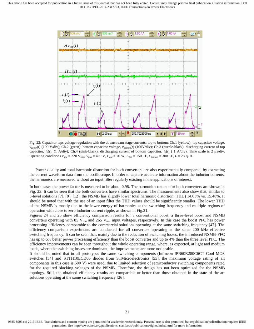
noted that at, as it can be seen from Fig.20, at low line inputs the converter mostly operates in mode 1 (or modes 1 and 2) causing most of the power to be transferred through the bottom portion of the downstream stage of Fig.14. To handle these conditions the transistor and the winding on the bottom primary side of the converter need to be designed such that thy can provide the full load power. This drawback is completely compensated by the fact that the transistor of the downstream stage operates at a three times smaller voltage than that of the conventional downstream solutions [2], [52]-[53], where most of the losses at the primary side of the converter are caused by high voltage stress of the transistors.
Hvbus(t)
vx(t)Vswing= 400 V
zoom
vin(t)
iL(t)0.375 A
Fig. 17: Key waveforms of the conventional boost-based PFC rectifier; top to bottom: Ch.1 (yellow): attenuated output voltage,
Hvbus(t) (2 V/div); Ch.2 (green): switching node voltage, vx(t) (200 V/div); Ch.3 (pink): input line current, iL(t) (0.5A/div); Ch.4
(purple): input line voltage, vin(t) (200 V/div). Time scale is 1 ms/div. Operating conditions: vline = 220 Vrms, Vbus = 400 V, Pout =
100 W, C = 100 F , L = 680 H.

0885-8993 (c) 2013 IEEE. Translations and content mining are permitted for academic research only. Personal use is also permitted, but republication/redistribution requires IEEEpermission. See http://www.ieee.org/publications_standards/publications/rights/index.html for more information.
This article has been accepted for publication in a future issue of this journal, but has not been fully edited. Content may change prior to final publication. Citation information: DOI10.1109/TPEL.2014.2317723, IEEE Transactions on Power Electronics
18
Hvbus(t)
mode 1
vx(t)
vin(t)
iL(t)
mode 2mode 3
mode 2 mode 1
zoom
133.3 V
266.6 V
0.125 A
133.3 V
Fig. 18: Key waveforms of the NSM-based PFC rectifier; top to bottom: Ch.1 (yellow): attenuated output voltage, Hvbus(t) (2
V/div); Ch.2 (green): switching node voltage, vx(t) (200 V/div); Ch.3 (pink): input line current, iL(t) (0.5A/div); Ch.4 (purple):
input line voltage, vin(t) (200 V/div). Time scale is 1 ms/div. Operating conditions vline = 220 Vrms, Vbus = 400 V, Pout = 100 W,
Ctop = 150 F, Cbottom= 300 F , L = 680 H.
Hvbus(t)
vx(t)Vswing= 400 V
zoom
vin(t)
iL(t)
0.375 A
Fig. 19: Key waveforms of the conventional boost-based PFC rectifier; top to bottom: Ch.1 (yellow): attenuated output voltage,
Hvbus(t) (2 V/div); Ch.2 (green): switching node voltage, vx(t) (200 V/div); Ch.3 (pink): input line current, iL(t) (0.5A/div); Ch.4
(purple): input line voltage, vin(t) (200 V/div). Time scale is 1 ms/div. Operating conditions: vline = 90 Vrms, Vbus = 400 V, Pout =
100 W, C = 100 F , L = 680 H.

0885-8993 (c) 2013 IEEE. Translations and content mining are permitted for academic research only. Personal use is also permitted, but republication/redistribution requires IEEEpermission. See http://www.ieee.org/publications_standards/publications/rights/index.html for more information.
This article has been accepted for publication in a future issue of this journal, but has not been fully edited. Content may change prior to final publication. Citation information: DOI10.1109/TPEL.2014.2317723, IEEE Transactions on Power Electronics
19
Hvbus(t)
vx(t)
vin(t)
iL(t)
mode 1
zoom
127.3 V
0.125 A
Vswing= 133 V
Fig. 20: Key waveforms of the conventional boost-based PFC rectifier; top to bottom: Ch.1 (yellow): attenuated output voltage,
Hvbus(t) (2 V/div); Ch.2 (green): switching node voltage, vx(t) (200 V/div); Ch.3 (pink): input line current, iL(t) (0.5A/div); Ch.4
(purple): input line voltage, vin(t) (200 V/div). Time scale is 1 ms/div. Operating conditions: vline = 90 Vrms, Vbus = 400 V, Pout =
100 W, C = 100 F , L = 680 H.

0885-8993 (c) 2013 IEEE. Translations and content mining are permitted for academic research only. Personal use is also permitted, but republication/redistribution requires IEEEpermission. See http://www.ieee.org/publications_standards/publications/rights/index.html for more information.
This article has been accepted for publication in a future issue of this journal, but has not been fully edited. Content may change prior to final publication. Citation information: DOI10.1109/TPEL.2014.2317723, IEEE Transactions on Power Electronics
20
c1(t)
vx(t)
vin(t)
d(t)=0
d(t)Ts
iL(t)
mode 1 mode 2
vx =Vbus/3
c2(t) d(t)≈ 1
Mode_signal
vx(t)
vin(t)
iL(t)
mode 2
d(t)Ts
mode 3
vx
d(t)=0 d(t)≈ 1
Mode_signal
Fig. 21: Transitions from mode 1 to mode 2 (top) and from mode 2 to mode 3 (bottom); Ch.1 (yellow): gating signal of SW2, c2(t)
(20 V/div); Ch.2 (green): switching node voltage, vx(t) (200V/div); Ch.3 (purple): input line current, iL(t), (0.5 A/div); Ch.4 (pink):
gating signal of SW1, c1(t) (20 V/div); Ch.m1(blue): input line voltage, vin(t) (200 V/div); digital input: mode control signal (0 =
mode 1, 1 = mode 2, 2 = mode 3). Time scale is 5 s/div. Operating conditions vline = 220 Vrms, Vbus = 400 V, Pout = 100 W, Ctop =
150 F, Cbottom = 300 F, L = 230 H.
0885-8993 (c) 2013 IEEE. Translations and content mining are permitted for academic research only. Personal use is also permitted, but republication/redistribution requires IEEEpermission. See http://www.ieee.org/publications_standards/publications/rights/index.html for more information.
This article has been accepted for publication in a future issue of this journal, but has not been fully edited. Content may change prior to final publication. Citation information: DOI10.1109/TPEL.2014.2317723, IEEE Transactions on Power Electronics
21
Hvtop(t)
Hvct(t)
i1(t)
i2(t)
i1(t)
i2(t)
Fig. 22: Capacitor taps voltage regulation with the downstream stage currents; top to bottom: Ch.1 (yellow): top capacitor voltage,
vupper(t) (100 V/div); Ch.2 (green): bottom capacitor voltage, vbottom(t) (100V/div); Ch.3 (purple-black): discharging current of top
capacitor, i1(t), (1 A/div); Ch.4 (pink-black): discharging current of bottom capacitor, i2(t) ( 1 A/div). Time scale is 2 s/div.
Operating conditions vline = 220 Vrms, Vbus = 400 V, Pout = 70 W, Ctop = 150 F, Cbottom = 300 F, L = 230 H.
Power quality and total harmonic distortion for both converters are also experimentally compared, by extracting
the current waveform data from the oscilloscope. In order to capture accurate information about the inductor currents,
the harmonics are measured without an input filter regularly existing in the applications of interest.
In both cases the power factor is measured to be about 0.98. The harmonic contents for both converters are shown in
Fig. 23. It can be seen that the both converters have similar spectrums. The measurements also show that, similar to
3-level solutions [7], [9], [12], the NSMB has slightly lower total harmonic distortion (THD) 14.03% vs. 15.48%. It
should be noted that with the use of an input filter the THD values should be significantly smaller. The lower THD
of the NSMB is mostly due to the lower energy of harmonics at the switching frequency and multiple regions of
operation with close to zero inductor current ripple, as shown in Fig.21.
Figures 24 and 25 show efficiency comparison results for a conventional boost, a three-level boost and NSMB
converters operating with 85 Vrms and 265 Vrms input voltages, respectively. In this case the boost PFC has power
processing efficiency comparable to the commercial solutions operating at the same switching frequency [47]. The
efficiency comparison experiments are conducted for all converters operating at the same 200 kHz effective
switching frequency. It can be seen that, mainly due to the reduction of switching losses, the introduced NSMB-PFC
has up to 6% better power processing efficiency than the boost converter and up to 4% than the three level PFC. The
efficiency improvements can be seen throughout the whole operating range, where, as expected, at light and medium
loads, where the switching losses are dominant, the improvements are more noticeable.
It should be noted that in all prototypes the same switching components (Infineon IPB60R280C6CT Cool MOS
switches [54] and STTH10LCD06 diodes from STMicroelectronics [55], the maximum voltage rating of all
components in this case is 600 V) were used, due to limited selection of semiconductor switching components rated
for the required blocking voltages of the NSMB. Therefore, the design has not been optimized for the NSMB
topology. Still, the obtained efficiency results are comparable or better than those obtained in the state of the art
solutions operating at the same switching frequency [26].

0885-8993 (c) 2013 IEEE. Translations and content mining are permitted for academic research only. Personal use is also permitted, but republication/redistribution requires IEEEpermission. See http://www.ieee.org/publications_standards/publications/rights/index.html for more information.
This article has been accepted for publication in a future issue of this journal, but has not been fully edited. Content may change prior to final publication. Citation information: DOI10.1109/TPEL.2014.2317723, IEEE Transactions on Power Electronics
22
101
102
103
0
0.9
0.95
1
0
0.05
0.1
0.15
0.85
≈
105
106
≈
≈
≈ ≈
No
rma
lize
d h
arm
onic
am
pli
tud
es
Frequency (Hz)
NSMB
101
0
0.9
0.95
1
0
0.05
0.1
0.15
0.85
≈
≈
≈
≈
105
106
≈
102
103
Frequency (Hz)
Norm
ali
zed h
arm
onic
am
pli
tudes
Conventional boost
Fig.23: Amplitudes of harmonics (multiples of 50 Hz) around line frequency and the switching frequency for the NSMB-based
PFC prototype (top) and the conventional boost based prototype (bottom).
Figures 26 and 27 compare the loss break down analysis for the boost, three level and NSMB converters. The loss
analysis results are shown for operation with input voltage of 265Vrms and 85Vrms for two cases of light (Fig.26) and
heavy (Fig.27) loads for each converter. Each bar in these figures shows the normalized losses from different
contributors to the overall losses of the corresponding converter and operating conditions.
It is also worth mentioning that most efficiency optimization techniques and volume reduction methods developed
for the conventional boost-based PFC topologies can be applied to the NSMB as well. Those include utilization of
super junction and SiC devices [18], variable frequency control [19], separate light load control scheme [20], [21],
and utilization of soft switching techniques [17]. For example, a soft-switched NSMB converter can be implemented
employing the ZVT circuit presented in [6]. This means that, in the NSMB, the benefits of all of these
complementary methods can be utilized while maintaining advantages of the smaller inductor and lower voltage
stress over the conventional solutions.
In the targeted cost-sensitive applications (below 500 W) the use of a bridgeless topology is usually avoided [13],
due to increased price and fairly limited relative improvements in the power processing efficiency. This can be
demonstrated by looking at the loss breakdown shown in Figs. 26 and 27. It can be seen that the diode bridge losses
of the NSMB converter are a very small portion of the overall losses at light loads (5.1%) and increase at heavy
loads, to 9.8%. The heavy load results indicate that for, higher power applications which are beyond the scope of this
work, the diode rectifier losses become more dominant and that the use of the bridgeless solution, shown in Fig. 16,
is fully justifiable.

0885-8993 (c) 2013 IEEE. Translations and content mining are permitted for academic research only. Personal use is also permitted, but republication/redistribution requires IEEEpermission. See http://www.ieee.org/publications_standards/publications/rights/index.html for more information.
This article has been accepted for publication in a future issue of this journal, but has not been fully edited. Content may change prior to final publication. Citation information: DOI10.1109/TPEL.2014.2317723, IEEE Transactions on Power Electronics
23
80
82
84
86
88
90
92
94
96
98
0 100 200 300 400
NSMB
BOOST
Three_Level
Eff
icie
ncy
(%
)
Output Power (W)
Fig.24: Efficiency comparison of the conventional boost, three level boost and NSMB PFC converters for the line input of 265
Vrms.
79
81
83
85
87
89
91
93
95
97
0 50 100 150 200 250 300 350 400
NSMB
Boost
Three_Level
Eff
icie
ncy
(%
)
Output Power (W)
Fig.25: Efficiency comparison of the conventional boost, three level boost and NSMB PFC converters for the line input of 85
Vrms.

0885-8993 (c) 2013 IEEE. Translations and content mining are permitted for academic research only. Personal use is also permitted, but republication/redistribution requires IEEEpermission. See http://www.ieee.org/publications_standards/publications/rights/index.html for more information.
This article has been accepted for publication in a future issue of this journal, but has not been fully edited. Content may change prior to final publication. Citation information: DOI10.1109/TPEL.2014.2317723, IEEE Transactions on Power Electronics
24
0
0.2
0.4
0.6
0.8
1
Boost
265Vrsm
Three level
265Vrsm
NSMB
90Vrsm
Boost
90Vrsm
Three level
90Vrsm
NSMB
265Vrsm
13.5
26.0
3.3
9.3
15.0
46.0
2.9
22.4
17.4
31.8
3.2
17.9
12.8
21.2
8.4
5.1
25.1
58.9
6.6
9.5
26.5
27.3
8.6
6.6
Switching losses
Core losses
Diode bridge losses
Conduction losses
Fig.26: Loss break down analysis for the conventional boost, three level boost and NSMB PFC converters for 85Vrms and 265
Vrms input voltages at the light load operating condition (50W). Length of each bar is normalized based on the losses of the boost
at 90Vrms which is 9.8W.
As mentioned before, in a potential implementation with custom-designed silicon components even larger efficiency
gains could be expected. This would mostly be due to the further reduction of switching losses, caused by increased
transistor speed and reduced values of parasitic capacitances of the semiconductor components.
The diagrams of Fig. 28 compare the volume breakdown between different components and total normalized
volumes of the conventional boost PFC, a two-phase interleaved boost based PFC [26], a three level PFC [6], and the
introduced NSMB-based solution for typical 300 W to 400 W applications [25], [26], [47]. The diagrams also show
volume comparisons for potential optimized implementations of the interleaved boost and NSMB, where the silicon
switches would be sized in accordance with their power ratings and implemented in a single package. As described
in Appendix A, such an optimized implementation would require the same silicon area as the conventional boost. It
Boost
265Vrsm
Three level
265Vrsm
NSMB
90Vrsm
Boost
90Vrsm
Three level
90Vrsm
NSMB
265Vrsm
Switching losses
Core losses
Diode bridge losses
Conduction losses
29.1
14.7
7.6
2.7
24.3
23.0
5.7
5.5
28.2
16.5
6.0
4.3
53.3
10.0
9.8
0.8
63.0
27.5
7.9
1.5
61.8
15.3
10.2
1.1
0
0.2
0.4
0.6
0.8
1
No
rmal
ized
Loss
es
Fig.27: Loss break down analysis for the conventional boost, three level boost and NSMB PFC converters for 85V rms and 265
Vrms input voltages at the light load operating condition (350W for 85Vrms and 400W for 265Vrms). Length of each bar is
normalized based on the losses of the boost at 90Vrms , which are 50.5W.

0885-8993 (c) 2013 IEEE. Translations and content mining are permitted for academic research only. Personal use is also permitted, but republication/redistribution requires IEEEpermission. See http://www.ieee.org/publications_standards/publications/rights/index.html for more information.
This article has been accepted for publication in a future issue of this journal, but has not been fully edited. Content may change prior to final publication. Citation information: DOI10.1109/TPEL.2014.2317723, IEEE Transactions on Power Electronics
25
0
0.1
0.2
0.3
0.4
0.5
0.6
0.7
0.8
0.9
1
Inductor
Output capacitor
Semiconductor
Heatsink
Controller
0.01
Conventional
boostInterleaved
Interleved with
optimized switches
No
rmal
ized
vo
lum
e
0.40
0.30
0.04
0.26
0.01
0.01
0.26
0.30
0.06
0.21
0.26
0.30
0.04
0.21
0.810.83
Three level Three level With
optimized switchesNSMB
0.06
0.13
0.30
0.21
0.01
0.70
NSMB with
optimized siwtches
0.01
0.13
0.30
0.21
0.04
0.69
0.01
0.20
0.30
0.22
0.780.01
0.20
0.30
0.22
0.76
0.040.06
Fig.28: Normalized volume distributions of conventional boost-based PFC and three other topologies; 2-phase interleaved
boost-based PFC, three level PFC, and the NSMB-based solution. In case of the latter three cases, a volume break down in
case of implementation with optimal switches, i.e. lower voltage/current rated switches in single package, is also shown.
should be noted that in these comparisons the input filter, whose volume significantly depends on the printed circuit
board (PCB) layout is not taken into account. However as indicated in the analysis of Subsection A.1.3, the required
volume of the NSMB input filter is smaller than that of the other analyzed solutions.
It can be seen that compared to the conventional boost, the NSMB has about 30% smaller total volume and is about
15 % smaller than the interleaved boost, which as shown in [25], has about 32% smaller inductor than the
conventional boost. The volume comparison results confirm discussions of the favorable
tradeoff from the previous sections. Since in the conventional boost a large portion of the volume of is occupied by
the inductor and the heat sink, about 65%, and less than a 5% by the semiconductors, a Trade-off between the
inductor reduction and efficiency improvement on one side and an increase in the semiconductor part numbers on the
other side is favorable. In this the semiconductor components include the diode bridge, which in the conventional
boost takes about 50% of the total silicon area, the diode and the transistor, which take the other 50%. The results
show that the three times reduction in the inductor volume and about a 12% in the heat sink volume, which is
proportional to the heat dissipation reduction, are more than compensating for about 50 % increase in the
semiconductor switch volume and a 60% increase in the volume in the controller size. In this case the size of the
controller is estimated by looking at the volume of analog components and the number of logic gates required for its
implementation for all three cases.
V. CONCLUSIONS
A rectifier with power factor correction based on a novel non-symmetric multi-level boost converter (NSMB) and a
complementary digital controller are introduced. In comparison with the conventional boost-based solutions, the
NSMB has three times smaller inductor as well as reduced switching losses. These advantages are achieved by
reducing the inductor, i.e. switching node, voltage swing to 1/3 of the conventional boost level. At the same time, the
voltage stress across the switching components is reduced to 1/3 for one diode-transistor pair and to 2/3 for the other
pair.
0885-8993 (c) 2013 IEEE. Translations and content mining are permitted for academic research only. Personal use is also permitted, but republication/redistribution requires IEEEpermission. See http://www.ieee.org/publications_standards/publications/rights/index.html for more information.
This article has been accepted for publication in a future issue of this journal, but has not been fully edited. Content may change prior to final publication. Citation information: DOI10.1109/TPEL.2014.2317723, IEEE Transactions on Power Electronics
26
The NSMB is a modified version of the three-level boost topology. Instead of having the same voltages across the
output divider capacitors, this modification uses a non-symmetric capacitor divider and the capacitor voltages are
regulated at 1/3 and 2/3 of the full output voltage level. As a result a 4-level operation is achieved reducing the
inductor by 33% without increasing the number of components required for implementation.
To control the capacitor voltages of the nonsymmetrical divider without using a bulky flying capacitor, an isolated
downstream converter is used. In regular operation, the downstream stage takes non-equal amounts of charge from
the capacitors keeping the capacitors voltage drops equal during discharging phases. The downstream converter stage
has two inputs and, similar to the NSMB, can utilize principles of the reduced voltage swings to obtain smaller
volume of magnetic components and reduced switching losses.
The mixed signal controller dynamically changes modes of the NSMB operation, depending on the instantaneous
input voltage value. Seamless transitions between 3 operating modes are provided through the digital PI compensator
re-initialization process, where depending on the type of transition, the current and stored previous values of duty
ratio are set to 0 or their maximum value. To eliminate the need for differential capacitor voltage measurements, a
switching state dependent sampling and hold technique is applied.
Results obtained with an experimental prototype verify that the NSMB converter requires a three times smaller
inductor and has significantly better power processing efficiency. The results also demonstrate stable controller
operation and seamless mode transitions.
It is important to note that the presented principle of the use of a non-symmetric voltage divider to create a 4-level
converter using 3-level hardware could potentially also be used in 3-level dc-ac converter applications to reduce the
volume of the inductive components.
VI. REFERENCES
[1] B. Sharifipour, J. S. Huang, P. Liao, L. Huber, and M. M. Jovanovic´, “Manufacturing and cost analysis of power-factor-
correction circuits,” in Proc. IEEE-APEC’98, Annu. Meeting, vol. 1, 1998, pp. 490-494.
[2] O. Garcia, J. A. Cobos, R. Prieto, P. Alou, and J. Uceda, “Power factor correction: A survey,” in Proc. IEEE PESC’01, 2001,
pp. 8–13.
[3] Y. Jang, M.M. Jovanovic, "Interleaved Boost Converter With Intrinsic Voltage-Doubler Characteristic for Universal-Line PFC
Front End," IEEE Trans. on Power Electron., vol.22, no.4, pp.1394-1401, July 2007
[4] J. Salmon, A. Knight, J. Ewanchuk, N. Noor, "Multi-level single phase boost rectifiers using coupled inductors," in Proc.
IEEE PESC 2008, pp.3156-3163.
[5] D. Maksimovic, R. Erickson, "Universal-input, high-power-factor, boost doubler rectifiers," in Proc. IEEE APEC '95, pp.459-
465 vol.1
[6] M.T. Zhang, Y. Jiang, F.C. Lee, M.M Jovanovic, "Single-phase three-level boost power factor correction converter ," in Proc.
IEEE APEC '95, pp.434-439 vol.1.
[7] F. Forest, T.A. Meynard, S. Faucher, F. Richardeau, J.J. Huselstein, C. Joubert, "Using the multilevel imbricated cells
topologies in the design of low-power power-factor-corrector converters," IEEE Trans. on Industrial Electronics, vol.52,
no.1, pp. 151- 161, Feb. 2005.
[8] D. Damasceno, L. Schuch, J.R. Pinheiro, "Design Procedure to Minimize Boost PFC Volume Concerning the Trade-offs
Among Switching Frequency, Input Current Ripple and Soft-Switching," in Proc. IEEE PESC '05. pp.2333-2338.
[9] Bor-Ren Lin, Tsung-Yu Yang, "Single-phase three-level converter for power factor correction," inProc. Circuits and Systems,
ISCAS '04., vol.5, pp.V-960-V-963.
[10] H. Keyhani, H.A. Toliyat, "Flying-capacitor boost converter," in Proc. IEEE APEC 2012, pp. 2311-2318.
[11] J. Salmon, A. Knight, J. Ewanchuk, N. Noor, "Multi-level single phase boost rectifiers using coupled inductors," in Proc.
IEEE PESC 2008, pp.3156-3163.
[12] T.A. Meynard, H. Foch, "Multi-level conversion: high voltage choppers and voltage-source inverters," in Proc. IEEE PESC
'92, pp.397-403 vol.1.
[13] L. Balogh, R. Redl, "Power-factor correction with interleaved boost converters in continuous-inductor-current mode," in
Proc. IEEE APEC '93. pp.168-174.
[14] P.W. Lee, Y.S. Lee, D.K.W. Cheng, and X.C. Liu, “Steady-State Analysis of an Interleaved Boost Converter with Coupled
Inductors,” IEEE Trans. on Industrial Electronics., vol. 47, no. 4, pp.787-795, Aug. 2000.

0885-8993 (c) 2013 IEEE. Translations and content mining are permitted for academic research only. Personal use is also permitted, but republication/redistribution requires IEEEpermission. See http://www.ieee.org/publications_standards/publications/rights/index.html for more information.
This article has been accepted for publication in a future issue of this journal, but has not been fully edited. Content may change prior to final publication. Citation information: DOI10.1109/TPEL.2014.2317723, IEEE Transactions on Power Electronics
27
[15] B.A. Miwa, D.M. Otten, M.E. Schlecht, "High efficiency power factor correction using interleaving techniques," in Proc.
IEEE APEC '92, pp.557-568.
[16] C. Wang, “Investigation on Interleaved Boost Converters and Applications,” PhD thesis, Virginia Polytechnic Institute and
State University, July 2009.
[17] Y. Jang; M.M. Jovanovic, K. Fang, Y. Chang, "High-power-factor soft-switched boost converter," IEEE Trans. on power
Electron., vol.21, no.1, pp.98-104, Jan. 2006
[18] F. Chimento, S. Musumeci, A. Raciti, M. Melito, G. Sorrentino, "Super-Junction MOSFET and SiC Diode Application for
the Efficiency Improvement in a Boost PFC Converter," in Proc. IEEE IECON ‘06, pp.2067-2072
[19] F. Chen, D. Maksimović, "Digital Control for Improved Efficiency and Reduced Harmonic Distortion Over Wide Load
Range in Boost PFC Rectifiers," ," IEEE Trans. on power Electron., vol.25, no.10, pp.2683-2692, Oct. 2010
[20] H. Kim, J. Kim; K. Park, H. Seong, G. Moon, M. Youn, "On/Off Control of Boost PFC Converters to Improve Light-Load
Efficiency in Paralleled Power Supply Units for Servers," IEEE Trans. on Ind. Electron., vol.61, no.3, pp.1235-1242, March
2014
[21] W. Wang; Y. Tzou, "Light load efficiency improvement for AC/DC boost PFC converters by digital multi-mode control
method," in Proc. IEEE PEDS ‘11, pp.1025-1030
[22] B. Mahdavikhah, R. Dicecco, and A. Prodic, “Low-volume PFC rectifier based on non-symmetric multi-level boost
converter,” in Proc. IEEE APEC 2013, pp. 1030-1034.
[23] R. W. Erickson and D. Maksimovic, Fundamentals of Power Electronics. New York, NY: Springer Media Inc., 2001.
[24] M.M. Jovanovic, J. Yungtaek, "State-of-the-art, single-phase, active power-factor-correction techniques for high-power
applications - an overview," IEEE Trans. on Industrial Electronics, vol.52, no.3, pp.701-708, June 2005.
[25] M. O’Loughlin, “An Interleaving PFC Pre-Regulator for High-Power Converters,” Texas Instruments Seminar,
http://www.ti.com/download/trng/docs/seminar/Topic5MO.pdf
[26] “UCC28070 300-W Interleaved PFC Pre-Regulator Design,” Texas Instruments, Application Note, July 2010.
[27] Qun Zhao; F.C. Lee, F.S. Tsai, "Voltage and current stress reduction in single-stage power factor correction AC/DC
converters with bulk capacitor voltage feedback," IEEE Trans. On Power Electron., vol.17, no.4, pp.477-484, Jul 2002
[28] R. Aparicio, A. Hajimiri. “Capacity limits and matching properties of lateral flux integrated capacitors,” in Proc. IEEE
Customs Integrated Circuits Conf., 2001, pp. 365-368, May 2001.
[29] D.Cochrance, “Passive Cancellation of Common-Mode Electromagnetic Interference in Switching Power Converters,”
M.Sc. thesis, Virginia Polytechnic Institute and State University, August 2010.
[30] J. Sun, M. Xu, Y Ying, F.C. Lee, "High Power Density, High Efficiency System Two-stage Power Architecture for Laptop
Computers," in Proc. IEEE PESC '06, pp.1-7.
[31] R.C.N. Pilawa-Podgurski, D.M. Giuliano, D.J. Perreault, “Merged two-stage power converter architecture with soft charging
switched-capacitor energy transfer,” in Proc. IEEE PESC 2008, pp. 4008-4015.
[32] A. Radić, A. Prodić, "Buck Converter With Merged Active Charge-Controlled Capacitive Attenuation," IEEE Trans. on
Power Electron., vol.27, no.3, pp.1049-1054, March 2012
[33] A. Prodic, "Digital Controller for High-Frequency Rectifiers with Power Factor Correction Suitable for On-Chip
Implementation," In Proc. PCC '07 , pp.1527-1531.
[34] S. Buso, P. Mattavelli, L. Rossetto, G. Spiazzi, "Simple digital control improving dynamic performance of power factor
preregulators," IEEE Trans. on Power Electron., vol. 18, Issue 5, pp. 814-823, Sep. 1998.
[35] A.H. Mitwalli, S.B. Leeb, G.C. Verghese, V.J. Thottuvelil, "An adaptive digital controller for a unity power factor converter
," IEEE Trans. on Power Electron., vol.11, no.2, pp.374-382, Mar 1996.
[36] A.Parayandeh, A. Prodic, "Programmable Analog-to-Digital Converter for Low-Power DC–DC SMPS," IEEE Trans. on
Power Electron., vol.23, no.1, pp.500-505, Jan. 2008.
[37] A. Prodic, D. Maksimovic, R.W. Erickson, "Design and implementation of a digital PWM controller for a high-frequency
switching DC-DC power converter," In Proc. IEEE IECON '01, vol.2, no., pp.893-898 vol.2.
[38] D.M. VandeSype, K. DeGusseme, F.M.L.L DeBelie,A.P. VandenBossche, J.A. Melkebeek, "Small-Signal -Domain
Analysis of Digitally Controlled Converters," IEEE Trans.on Power Electron., vol.21, no.2, pp.470-478, March 2006.
[39] Z. Zhenyu; A. Prodic, P. Mattavelli, "Self-Programmable PID Compensator for Digitally Controlled SMPS," in Proc. IEEE
COMPEL '06. pp.112-116.

0885-8993 (c) 2013 IEEE. Translations and content mining are permitted for academic research only. Personal use is also permitted, but republication/redistribution requires IEEEpermission. See http://www.ieee.org/publications_standards/publications/rights/index.html for more information.
This article has been accepted for publication in a future issue of this journal, but has not been fully edited. Content may change prior to final publication. Citation information: DOI10.1109/TPEL.2014.2317723, IEEE Transactions on Power Electronics
28
[40] B.T. Lynch, “Under the Hood of a DC/DC Boost Converter,” presented at the TI Power Supply Design Seminar, Dallas, TX,
2008-2009, Paper SEM1800.
[41] R.B. Standler, “Protection of Electronic Circuits from Overvoltages”, Courier Dover Publications, 2002.
[42] M. Allen, “Understanding power supplies and inrush current,” Bear Power Supplies, Electronic Products, January 2006.
[43] C. Glaser, “Extending Soft Start Time in TPS6107x Family of Boost Converters,” Texas Instruments Application Report
SLVA307, August 2008.
[44] Kislovski, A.S., "Fast active inrush current limiter for boost-based resistor emulators," In Proc. INTELEC '94., pp.649-652.
[45] F. Musavi, W. Eberle, W.G. Dunford, “A High-Performance Single-Phase Bridgeless Interleaved PFC Converter for Plug-in
Hybrid Electric Vehicle Battery Chargers, “ IEEE Transactions on Industry Applications, vol. 47, Issue 4, pp. 1833 – 1843,
July/August 2011.
[46] D.M. Mitchell,"AC-DC Converter having an improved power factor", U.S. Patent 4,412,277, Oct. 25, 1983.
[47] M. Scherf, W. Frank, “200W SMPS Demonstration Board II,” Infineon Technologies, Application Note AN- CoolMOS 09,
2004.
[48] “CTX-10 Series Low-Cost Power Inductors, ” Cooper Bussmann, Datasheet, 2007.
[49] “PCV-2 Inductor Series,” Coilcraft, Datasheet, 2014.
[50] “CTX-16-17769 inductor, ” Cooper Bussmann, Datasheet.
[51] H. Peng; D. Maksimovic; A. Prodic; E. Alarcon, "Modeling of quantization effects in digitally controlled DC-DC
converters," In Proc. IEEE PESC 04, vol.6, pp.4312-4318.
[52] J. Sebastian, P. Villegas, F. Nuno, M.M. Hernando, "Very efficient two-input DC-to-DC switching post-regulators,"in Proc.
IEEE PESC'96, pp. 874-880, 2006.
[53] G. Spiazzi, "Analysis of buck converters used as power factor pre-regulators," in Proc. IEEE PESC '97, pp.564-570, 1997.
[54] “IPx65R660CFD CoolMOS CFD2 Power Transistor, ” Infenion Technologies AG, Datasheet, 2011.
[55] “STTH10LCD06 ultra fast diode, ” STMicroelectronics, Datasheet, 2010.
[56] B.J. Baliga, “FUNDAMENTALS OF POWER SEMICONDUCTOR DEVICES,” NEWYORK, NY: SPRINGER, 2008.
APPENDIX A
ANALYSIS OF CONDUCTION LOSSES FOR OPTIMIZED DESIGN OF SWITCHING COMPONENTS
The following analysis and comparison of the conduction losses is based on the assumption that the semiconductor
components of the both converters are sized in accordance with their voltage ratings.
A. Analytical comparison of Conduction losses
The conduction losses corresponding to the boost PFC converter can approximately be described with the following
equation [23]:
dtt D't i V +t D ti R+ti R=P boostLFT
0 boost2Lon
2LLboostboostcond,
L )]()()()()([ , (A1)
where TL is time duration of a half line cycle, iL(t) is the inductor current, RLboost is a resistance that models total
inductor losses, Ron is the on resistance of the transistor, VF is the diode forward voltage drop and Dboost is the boost
converter duty cycle.
For the NSMB converter, due to the change of conduction path based on the converter operating mode (shown in
Figs. 3 to 5), the losses are described with three different equations, corresponding to three distinctive modes of
work.

0885-8993 (c) 2013 IEEE. Translations and content mining are permitted for academic research only. Personal use is also permitted, but republication/redistribution requires IEEEpermission. See http://www.ieee.org/publications_standards/publications/rights/index.html for more information.
This article has been accepted for publication in a future issue of this journal, but has not been fully edited. Content may change prior to final publication. Citation information: DOI10.1109/TPEL.2014.2317723, IEEE Transactions on Power Electronics
29
dtt D't i VtiR+t D tiRR+ti R=P NSMB,1LF22Lon,1
TNSMB,1
2Lon,2on,1
2LLNSMBNSMB,1cond,
1
)]() )()(( )()()()([ , (A2)
dtt D't i VtiR +tD t i VtiR+ti R=P NSMB,2LF12Lon,2
TNSMB,2LF2
2Lon,1
2LLNSMBNSMB,2cond,
2
)]() )()(()() )()(()([ , (A3)
dtt D't i Vti VtDt i VtiR+ti R=P NSMB,3LF2LF1T
NSMB,3LF12Lon,2
2LLNSMBNSMB,3cond,
3
)]() )()( ()( ) )()(()([ , (A4)
where Ti represents the time converter operates in mode i during a half of line cycle, RLNSMB is equivalent resistance
of the NSMB inductor modeling its core and copper losses, Ron is the on resistance of Qi, VFi is forward voltage drop
of the diode Di, and DNSMB,i corresponds to the duty ratio of the NSMB converter during mode i.
The total conduction losses can be found as the sum of the previous three equations:
NSMB,3cond,NSMB,2cond,NSMB,1cond,NSMBcond, PPP=P , (A5)
By utilizing volt-second balance [23], the following relations between duty cycles of the boost and the NSMB can be
found:
2-t 3Dt D boostNSMB,1 )()( (A6)
1-t 3Dt D boostNSMB,2 )()( (A7)
)()( t 3Dt D boostNSMB,3 . (A8)
Assuming that area used for implementing the transistors of the NSMB is the same as that needed for the boost
transistor and taking into account that the on resistance of a power a mosfet per unit silicon area is given by [56] 2
_ . Bspon VR , (A9)
where α is a process-dependent constant and VB is the breakdown voltage, the following relations between the on
resistances of the mosfet resistances can be found:
onon,1 R9
4R (A10)
onon,2 R9
1R , (A11)
where Ron is the resistance of the boost transistor and Ron,1 are Ron,2 are the resistances of the NSMB. The equations
are obtained by taking into account that the blocking voltages of Q1 and Q2 are a 66% and a 33% of that of the boost
transistor, respectively.
By substituting equations A6 to A11 into Eq.A5 and assuming that the forward voltage drops of all diodes are the
same, the following relation between the conduction losses of the two topologies is obtained:
L
1
1
T
LLNSMBLboost
T3
2
Lonboost
T2
2
Lon
T
2
Lonboost
T3
LboostFF
T2
LboostF
T
Lboost'
Fboostcond,NSMBcond,
ttiRR
tdt iRtD3
dtt iR9
dtt iR)9
tD3
dtt itDVV dtt itDVdtt itDVP=P
0
2 )d( )-(
)()(2
)(2
)(2
-)(2
(
)()](2[)()()()(2
, (A12)
The results show that the diodes losses of the NSMB are slightly higher. The value of the diode losses depends on
the input voltage level, i.e. on the portions of time the NSMB spend in each mode of operation. However, these extra
losses can be partially or completely compensated by the smaller transistor conduction losses and also smaller
inductance of the NSMB resulting in lower copper and conduction losses.