lp2980 micropower 50 ma ultra low-dropout...
TRANSCRIPT

LP2980Micropower 50 mA Ultra Low-Dropout Regulator InSOT-23 and micro SMD PackagesGeneral DescriptionThe LP2980 is a 50 mA, fixed-output voltage regulator de-signed specifically to meet the requirements of battery-powered applications.
Using an optimized VIP™ (Vertically Integrated PNP) pro-cess, the LP2980 delivers unequaled performance in allspecifications critical to battery-powered designs:
Dropout Voltage. Typically 120 mV @ 50 mA load, and 7 mV@ 1 mA load.
Ground Pin Current. Typically 375 µA @ 50 mA load, and 80µA @ 1 mA load.
Sleep Mode. Less than 1 µA quiescent current when ON/OFF pin is pulled low.
Smallest Possible Size. SOT-23 and micro SMD packagesuse an absolute minimum board space.
Minimum Part Count. Requires only 1 µF of external ca-pacitance on the regulator output.
Precision Output. 0.5% tolerance output voltages available(A grade).
5.0V, 3.3V, and 3.0V versions available as standard prod-ucts.
Featuresn Ultra low dropout voltagen Output voltage accuracy 0.5% (A Grade)n Guaranteed 50 mA output currentn Smallest possible size (SOT-23, micro SMD package)n Requires only 1 µF external capacitancen < 1 µA quiescent current when shutdownn Low ground pin current at all load currentsn High peak current capability (150 mA typical)n Wide supply voltage range (16V max)n Fast dynamic response to line and loadn Low ZOUT over wide frequency rangen Overtemperature/overcurrent protectionn −40˚C to +125˚C junction temperature range
Applicationsn Cellular Phonen Palmtop/Laptop Computern Personal Digital Assistant (PDA)n Camcorder, Personal Stereo, Camera
Block Diagram
01207801
VIP™ is a trademark of National Semiconductor Corporation.
January 2003LP
2980M
icropower
50m
AU
ltraLow
-Dropout
Regulator
InS
OT-23
andm
icroS
MD
Packages
© 2003 National Semiconductor Corporation DS012078 www.national.com

Connection Diagram and Ordering Information5-Lead Small Outline Package (M5) micro SMD, 5 Bump Package (BPA05)
01207803
Top ViewSee NS Package Number MF05A
For ordering information see Table 101207864
Note: The actual physical placement of the package marking will vary frompart to part. Package marking contains date code and lot traceabilityinformation, and will vary considerably. Package marking does not correlateto device type.
Top ViewSee NS Package Number BPA05
Pin Descrption
Name Pin Number Function
SOT-23 micro SMD
VIN 1 C3 Input Voltage
GND 2 A1 Common Ground (device substrate)
ON/OFF 3 A3 Logic high enable input
N/C 4 B2 Post package trim - do not connect to this pin
VOUT 5 C1 Regulated output voltage
Ordering InformationTABLE 1. Package Marking and Order Information
Output Voltage(V)
Grade Order Information PackageMarking
Supplied as:
5-Lead Small Outline Package (M5)
For output voltages ≤ 2.3V, refer to LP2980LV datasheet. If a non-standard voltage is required, see LP2980-ADJ.
2.5 A LP2980AIM5X-2.5 L0NA 3000 Units on Tape and Reel
2.5 A LP2980AIM5-2.5 L0NA 1000 Units on Tape and Reel
2.5 STD LP2980IM5X-2.5 L0NB 3000 Units on Tape and Reel
2.5 STD LP2980IM5-2.5 L0NB 1000 Units on Tape and Reel
2.6 A LP2980AIM5X-2.6 L48A 3000 Units on Tape and Reel
2.6 A LP2980AIM5-2.6 L48A 1000 Units on Tape and Reel
2.6 STD LP2980IM5X-2.6 L48B 3000 Units on Tape and Reel
2.6 STD LP2980IM5-2.6 L48B 1000 Units on Tape and Reel
2.7 A LP2980AIM5X-2.7 L26A 3000 Units on Tape and Reel
2.7 A LP2980AIM5-2.7 L26A 1000 Units on Tape and Reel
2.7 STD LP2980IM5X-2.7 L26B 3000 Units on Tape and Reel
2.7 STD LP2980IM5-2.7 L26B 1000 Units on Tape and Reel
2.8 A LP2980AIM5X-2.8 L13A 3000 Units on Tape and Reel
2.8 A LP2980AIM5-2.8 L13A 1000 Units on Tape and Reel
2.8 STD LP2980IM5X-2.8 L13B 3000 Units on Tape and Reel
2.8 STD LP2980IM5-2.8 L13B 1000 Units on Tape and Reel
2.9 A LP2980AIM5X-2.9 L12A 3000 Units on Tape and Reel
2.9 A LP2980AIM5-2.9 L12A 1000 Units on Tape and Reel
2.9 STD LP2980IM5X-2.9 L12B 3000 Units on Tape and Reel
LP29
80
www.national.com 2

Ordering Information (Continued)
TABLE 1. Package Marking and Order Information (Continued)
Output Voltage(V)
Grade Order Information PackageMarking
Supplied as:
2.9 STD LP2980IM5-2.9 L12B 1000 Units on Tape and Reel
3.0 A LP2980AIM5X-3.0 L02A 3000 Units on Tape and Reel
3.0 A LP2980AIM5-3.0 L02A 1000 Units on Tape and Reel
3.0 STD LP2980IM5X-3.0 L02B 3000 Units on Tape and Reel
3.0 STD LP2980IM5-3.0 L02B 1000 Units on Tape and Reel
3.1 A LP2980AIM5X-3.1 L30A 3000 Units on Tape and Reel
3.1 A LP2980AIM5-3.1 L30A 1000 Units on Tape and Reel
3.1 STD LP2980IM5X-3.1 L30B 3000 Units on Tape and Reel
3.1 STD LP2980IM5-3.1 L30B 1000 Units on Tape and Reel
3.2 A LP2980AIM5X-3.2 L31A 3000 Units on Tape and Reel
3.2 A LP2980AIM5-3.2 L31A 1000 Units on Tape and Reel
3.2 STD LP2980IM5X-3.2 L31B 3000 Units on Tape and Reel
3.2 STD LP2980IM5-3.2 L31B 1000 Units on Tape and Reel
3.3 A LP2980AIM5X-3.3 L00A 3000 Units on Tape and Reel
3.3 A LP2980AIM5-3.3 L00A 1000 Units on Tape and Reel
3.3 STD LP2980IM5X-3.3 L00B 3000 Units on Tape and Reel
3.3 STD LP2980IM5-3.3 L00B 1000 Units on Tape and Reel
3.5 A LP2980AIM5X-3.5 L27A 3000 Units on Tape and Reel
3.5 A LP2980AIM5-3.5 L27A 1000 Units on Tape and Reel
3.5 STD LP2980IM5X-3.5 L27B 3000 Units on Tape and Reel
3.5 STD LP2980IM5-3.5 L27B 1000 Units on Tape and Reel
3.6 A LP2980AIM5X-3.6 L28A 3000 Units on Tape and Reel
3.6 A LP2980AIM5-3.6 L28A 1000 Units on Tape and Reel
3.6 STD LP2980IM5X-3.6 L28B 3000 Units on Tape and Reel
3.6 STD LP2980IM5-3.6 L28B 1000 Units on Tape and Reel
3.8 A LP2980AIM5X-3.8 L21A 3000 Units on Tape and Reel
3.8 A LP2980AIM5-3.8 L21A 1000 Units on Tape and Reel
3.8 STD LP2980IM5X-3.8 L21B 3000 Units on Tape and Reel
3.8 STD LP2980IM5-3.8 L21B 1000 Units on Tape and Reel
4.0 A LP2980AIM5X-4.0 L25A 3000 Units on Tape and Reel
4.0 A LP2980AIM5-4.0 L25A 1000 Units on Tape and Reel
4.0 STD LP2980IM5X-4.0 L25B 3000 Units on Tape and Reel
4.0 STD LP2980IM5-4.0 L25B 1000 Units on Tape and Reel
4.5 A LP2980AIM5X-4.5 L0XA 3000 Units on Tape and Reel
4.5 A LP2980AIM5-4.5 L0XA 1000 Units on Tape and Reel
4.5 STD LP2980IM5X-4.5 L0XB 3000 Units on Tape and Reel
4.5 STD LP2980IM5-4.5 L0XB 1000 Units on Tape and Reel
4.7 A LP2980AIM5X-4.7 L37A 3000 Units on Tape and Reel
4.7 A LP2980AIM5-4.7 L37A 1000 Units on Tape and Reel
4.7 STD LP2980IM5X-4.7 L37B 3000 Units on Tape and Reel
4.7 STD LP2980IM5-4.7 L37B 1000 Units on Tape and Reel
5.0 A LP2980AIM5X-5.0 L01A 3000 Units on Tape and Reel
5.0 A LP2980AIM5-5.0 L01A 1000 Units on Tape and Reel
5.0 STD LP2980IM5X-5.0 L01B 3000 Units on Tape and Reel
5.0 STD LP2980IM5-5.0 L01B 1000 Units on Tape and Reel
micro SMD, 5 Bump Package (BPA05)
3.3 A LP2980AIBP-3.3 250 Units on Tape and Reel
LP2980
www.national.com3

Ordering Information (Continued)
TABLE 1. Package Marking and Order Information (Continued)
Output Voltage(V)
Grade Order Information PackageMarking
Supplied as:
3.3 A LP2980AIBPX-3.3 3000 Units on Tape and Reel
3.3 STD LP2980IBP-3.3 250 Units on Tape and Reel
3.3 STD LP2980IBPX-3.3 3000 Units on Tape and Reel
5.0 A LP2980AIBP-5.0 250 Units on Tape and Reel
5.0 A LP2980AIBPX-5.0 3000 Units on Tape and Reel
5.0 STD LP2980IBP-5.0 250 Units on Tape and Reel
5.0 STD LP2980IBPX-5.0 3000 Units on Tape and Reel
LP29
80
www.national.com 4

Absolute Maximum Ratings (Note 1)
If Military/Aerospace specified devices are required,please contact the National Semiconductor Sales Office/Distributors for availability and specifications.
Storage Temperature Range −65˚C to +150˚C
Operating Junction Temperature
Range −40˚C to +125˚C
Lead Temperature
(Soldering, 5 sec.) 260˚C
ESD Rating (Note 2) 2 kV
Power Dissipation (Note 3) Internally Limited
Input Supply Voltage (Survival) −0.3V to +16V
Input Supply Voltage (Operating) 2.1V to +16V
Shutdown Input Voltage(Survival) −0.3V to +16V
Output Voltage (Survival), (Note4) −0.3V to +9V
IOUT (Survival) Short Circuit Protected
Input-Output Voltage (Survival),
(Note 5) −0.3V to +16V
Electrical Characteristics (Note 10)
Limits in standard typeface are for TJ = 25˚C, and limits in boldface type apply over the full operating temperature range. Un-less otherwise specified: VIN = VO(NOM) + 1V, IL = 1 mA, COUT = 1 µF, VON/OFF = 2V.
Symbol Parameter Conditions Typ LP2980AI-XX LP2980I-XX Units
(Note 6) (Note 6)
Min Max Min Max
∆VO Output VoltageTolerance
IL = 1 mA −0.50 0.50 −1.0 1.0
%VNOM1 mA < IL < 50 mA −0.75 0.75 −1.5 1.5
−2.5 2.5 −3.5 3.5
Output Voltage VO(NOM) + 1V 0.007 0.014 0.014 %/V
Line Regulation ≤ VIN ≤ 16V 0.032 0.032
VIN–VO Dropout Voltage IL = 0 1 3 3 mV
(Note 7) 5 5
IL = 1 mA 7 10 10
15 15
IL = 10 mA 40 60 60
90 90
IL = 50 mA 120 150 150
225 225
IGND Ground Pin Current IL = 0 65 95 95 µA
125 125
IL = 1 mA 80 110 110
170 170
IL = 10 mA 140 220 220
460 460
IL = 50 mA 375 600 600
1200 1200
VON/OFF < 0.18V 0 1 1
VON/OFF ON/OFF Input Voltage High = O/P ON 1.4 1.6 1.6 V
(Note 8) Low = O/P OFF 0.55 0.18 0.18
ION/OFF ON/OFF Input Current VON/OFF = 0 0 −1 −1 µA
VON/OFF = 5V 5 15 15
IO(PK) Peak Output Current VOUT ≥ VO(NOM) − 5% 150 100 100 mA
en Output Noise BW = 300 Hz–50 kHz, 160 µV
Voltage (RMS) COUT = 10 µF
Ripple Rejection f = 1 kHz 63 dB
COUT = 10 µF
IO(MAX) Short Circuit Current RL = 0 (Steady State)(Note 9)
150 mA
LP2980
www.national.com5

Electrical Characteristics (Note 10) (Continued)Note 1: Absolute maximum ratings indicate limits beyond which damage to the component may occur. Electrical specifications do not apply when operating thedevice outside of its rated operating conditions.
Note 2: The ESD rating of pins 3 and 4 for the SOT-23 package, or pins 5 and 2 for the micro SMD package, is 1 kV.
Note 3: The maximum allowable power dissipation is a function of the maximum junction temperature, TJ(MAX), the junction-to-ambient thermal resistance, θJA, andthe ambient temperature, TA. The maximum allowable power dissipation at any ambient temperature is calculated using:
The value of θJA for the SOT-23 package is 220˚C/W and the micro SMD package is 255˚C/W. Exceeding the maximum allowable power dissipation will causeexcessive die temperature, and the regulator will go into thermal shutdown.
Note 4: If used in a dual-supply system where the regulator load is returned to a negative supply, the LP2980 output must be diode-clamped to ground.
Note 5: The output PNP structure contains a diode between the VIN and VOUT terminals that is normally reverse-biased. Reversing the polarity from VIN to VOUTwill turn on this diode (see Application Hints).
Note 6: Limits are 100% production tested at 25˚C. Limits over the operating temperature range are guaranteed through correlation using Statistical Quality Control(SQC) methods. The limits are used to calculate National’s Average Outgoing Quality Level (AOQL).
Note 7: Dropout voltage is defined as the input to output differential at which the output voltage drops 100 mV below the value measured with a 1V differential.
Note 8: The ON/OFF inputs must be properly driven to prevent misoperation. For details, refer to Application Hints.
Note 9: See Typical Performance Characteristics curves.
Note 10: Exposing the micro SMD device to direct sunlight will cause misoperation. See Application Hints for additional information.
Basic Application Circuit
01207802
*ON/OFF input must be actively terminated. Tie to VIN if this function is not to be used.
**Minimum Output Capacitance is 1 µF to insure stability over full load current range. More capacitance provides superior dynamic performance and additionalstability margin (see Application Hints).
***Do not make connections to this pin.
LP29
80
www.national.com 6

Typical Performance Characteristics Unless otherwise specified: TA = 25˚C, VIN = VO(NOM) + 1V,COUT = 2.2 µF, all voltage options, ON/OFF pin tied to VIN.
Output Voltage vsTemperature
Output Voltage vsTemperature
01207809 01207839
Output Voltage vsTemperature Dropout Characteristics
01207840 01207816
Dropout Characteristics Dropout Characteristics
0120781501207814
LP2980
www.national.com7
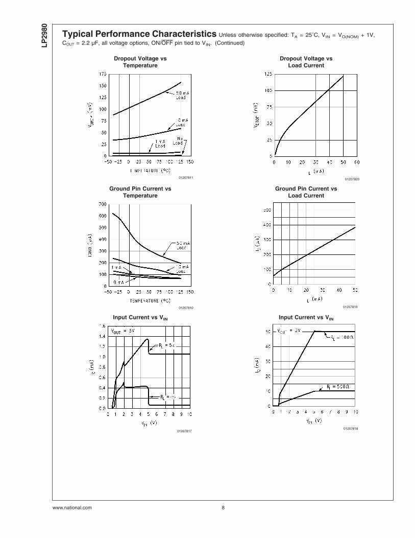
Typical Performance Characteristics Unless otherwise specified: TA = 25˚C, VIN = VO(NOM) + 1V,COUT = 2.2 µF, all voltage options, ON/OFF pin tied to VIN. (Continued)
Dropout Voltage vsTemperature
Dropout Voltage vsLoad Current
01207811 01207820
Ground Pin Current vsTemperature
Ground Pin Current vsLoad Current
01207810 01207819
Input Current vs VIN Input Current vs VIN
0120781701207818
LP29
80
www.national.com 8
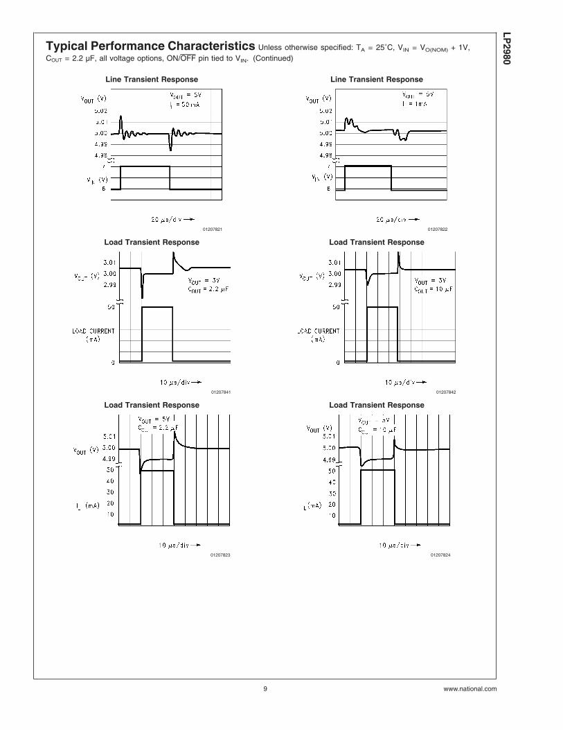
Typical Performance Characteristics Unless otherwise specified: TA = 25˚C, VIN = VO(NOM) + 1V,COUT = 2.2 µF, all voltage options, ON/OFF pin tied to VIN. (Continued)
Line Transient Response Line Transient Response
01207821 01207822
Load Transient Response Load Transient Response
01207841 01207842
Load Transient Response Load Transient Response
01207823 01207824
LP2980
www.national.com9
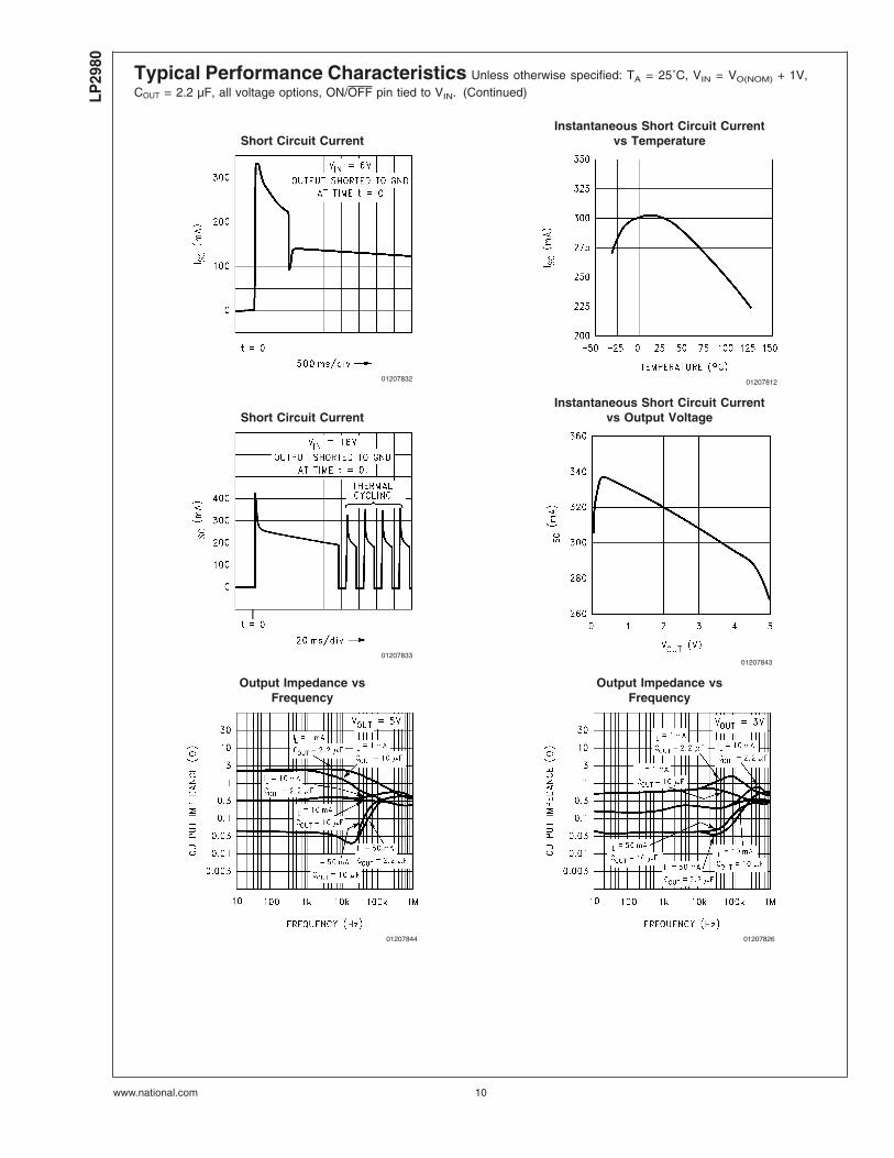
Typical Performance Characteristics Unless otherwise specified: TA = 25˚C, VIN = VO(NOM) + 1V,COUT = 2.2 µF, all voltage options, ON/OFF pin tied to VIN. (Continued)
Short Circuit CurrentInstantaneous Short Circuit Current
vs Temperature
01207832 01207812
Short Circuit CurrentInstantaneous Short Circuit Current
vs Output Voltage
0120783301207843
Output Impedance vsFrequency
Output Impedance vsFrequency
01207844 01207826
LP29
80
www.national.com 10
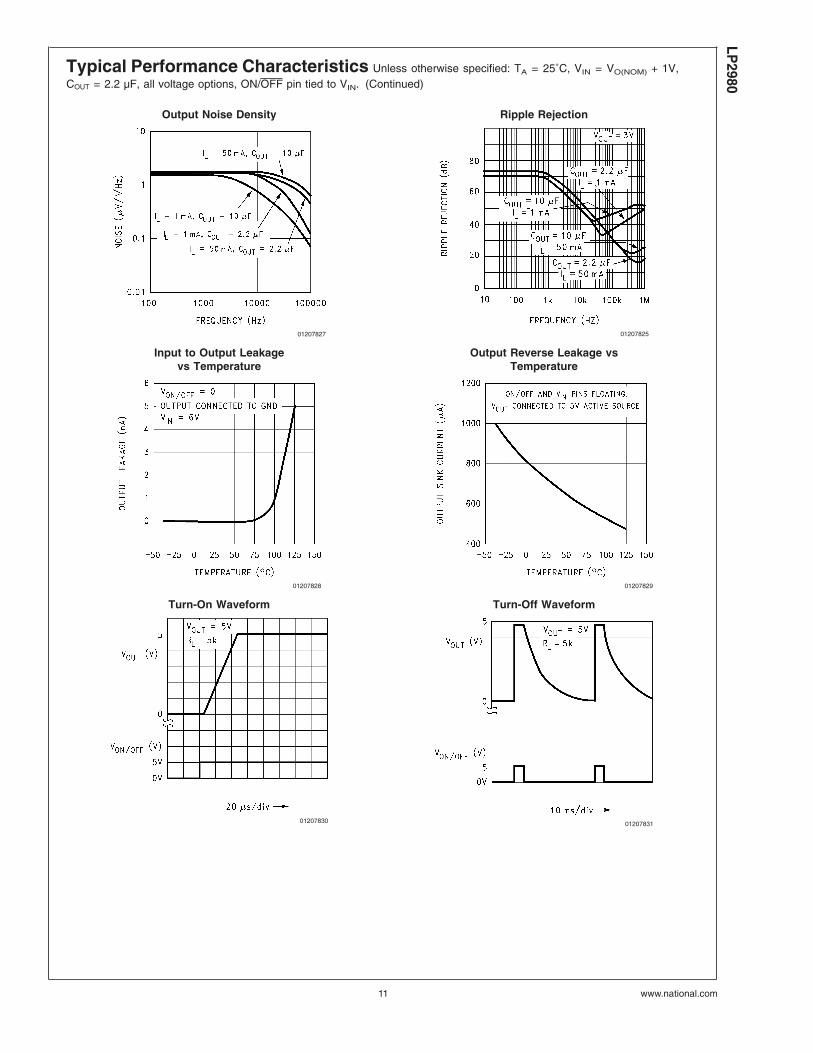
Typical Performance Characteristics Unless otherwise specified: TA = 25˚C, VIN = VO(NOM) + 1V,COUT = 2.2 µF, all voltage options, ON/OFF pin tied to VIN. (Continued)
Output Noise Density Ripple Rejection
01207827 01207825
Input to Output Leakagevs Temperature
Output Reverse Leakage vsTemperature
01207828 01207829
Turn-On Waveform Turn-Off Waveform
01207830 01207831
LP2980
www.national.com11

Typical Performance Characteristics Unless otherwise specified: TA = 25˚C, VIN = VO(NOM) + 1V,COUT = 2.2 µF, all voltage options, ON/OFF pin tied to VIN. (Continued)
ON/OFF Pin Current vs VON/OFF
01207845
LP29
80
www.national.com 12
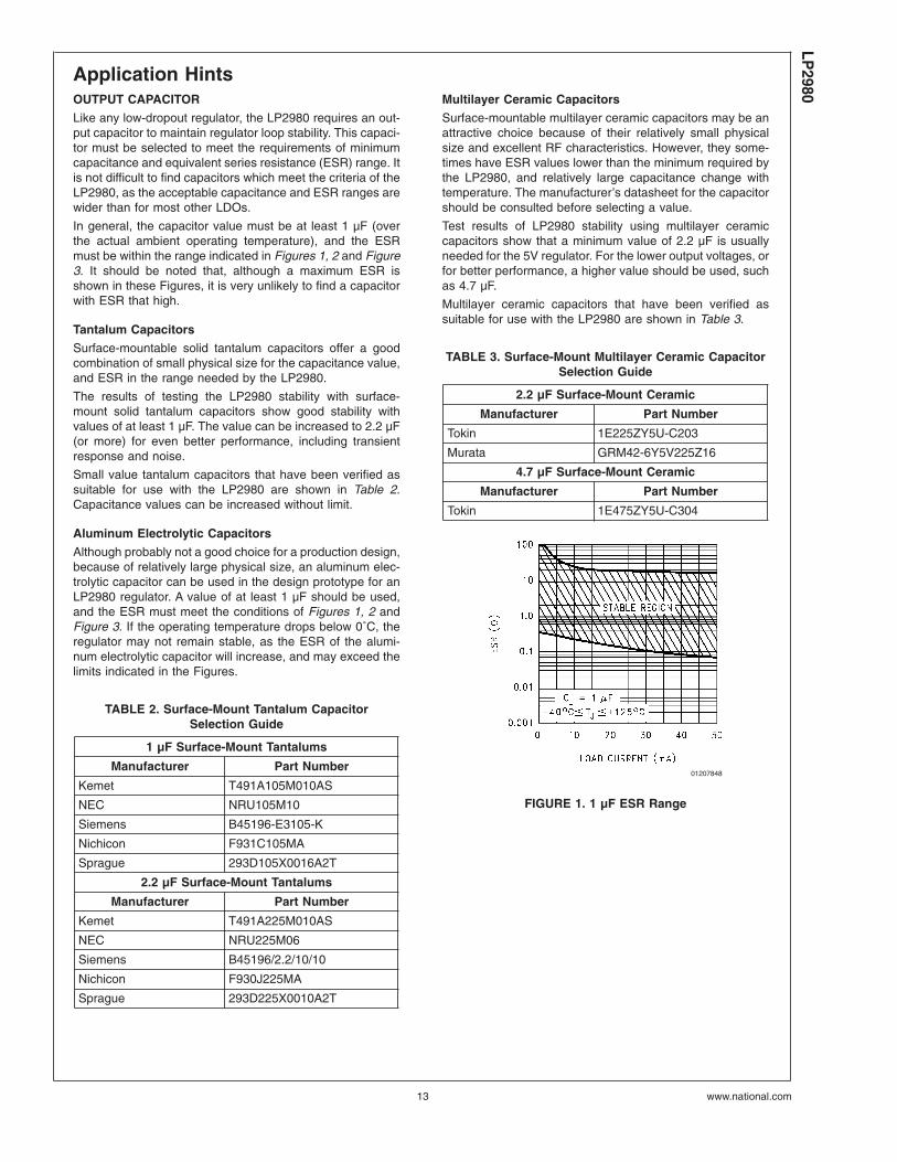
Application HintsOUTPUT CAPACITOR
Like any low-dropout regulator, the LP2980 requires an out-put capacitor to maintain regulator loop stability. This capaci-tor must be selected to meet the requirements of minimumcapacitance and equivalent series resistance (ESR) range. Itis not difficult to find capacitors which meet the criteria of theLP2980, as the acceptable capacitance and ESR ranges arewider than for most other LDOs.
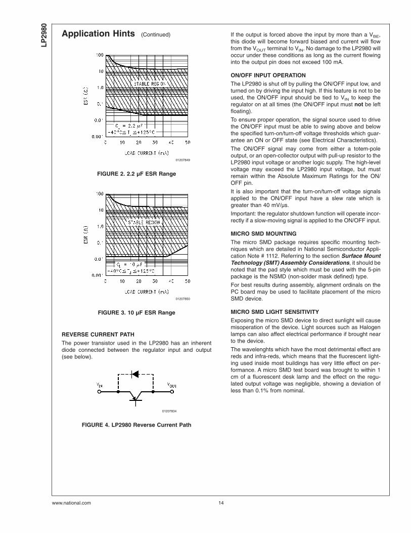
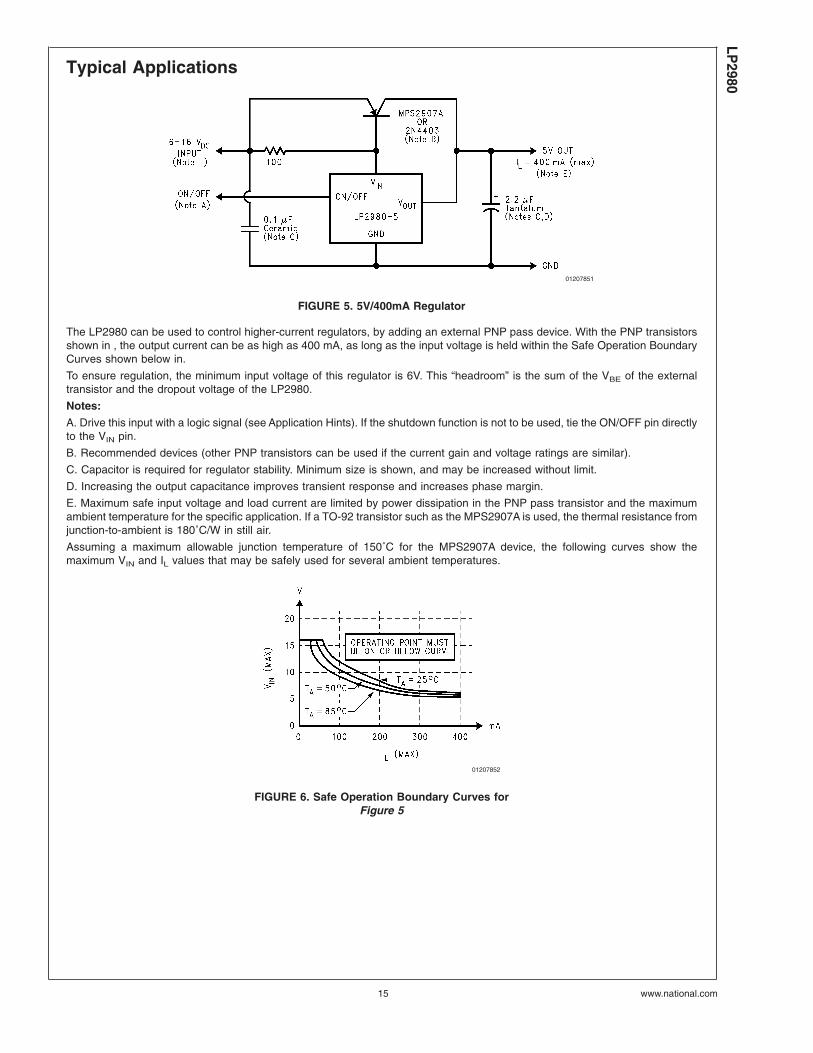
In general, the capacitor value must be at least 1 µF (overthe actual ambient operating temperature), and the ESRmust be within the range indicated in Figures 1, 2 and Figure3. It should be noted that, although a maximum ESR isshown in these Figures, it is very unlikely to find a capacitorwith ESR that high.
Tantalum Capacitors
Surface-mountable solid tantalum capacitors offer a goodcombination of small physical size for the capacitance value,and ESR in the range needed by the LP2980.
The results of testing the LP2980 stability with surface-mount solid tantalum capacitors show good stability withvalues of at least 1 µF. The value can be increased to 2.2 µF(or more) for even better performance, including transientresponse and noise.
Small value tantalum capacitors that have been verified assuitable for use with the LP2980 are shown in Table 2.Capacitance values can be increased without limit.
Aluminum Electrolytic Capacitors
Although probably not a good choice for a production design,because of relatively large physical size, an aluminum elec-trolytic capacitor can be used in the design prototype for anLP2980 regulator. A value of at least 1 µF should be used,and the ESR must meet the conditions of Figures 1, 2 andFigure 3. If the operating temperature drops below 0˚C, theregulator may not remain stable, as the ESR of the alumi-num electrolytic capacitor will increase, and may exceed thelimits indicated in the Figures.
TABLE 2. Surface-Mount Tantalum CapacitorSelection Guide
1 µF Surface-Mount Tantalums
Manufacturer Part Number
Kemet T491A105M010AS
NEC NRU105M10
Siemens B45196-E3105-K
Nichicon F931C105MA
Sprague 293D105X0016A2T
2.2 µF Surface-Mount Tantalums
Manufacturer Part Number
Kemet T491A225M010AS
NEC NRU225M06
Siemens B45196/2.2/10/10
Nichicon F930J225MA
Sprague 293D225X0010A2T
Multilayer Ceramic Capacitors
Surface-mountable multilayer ceramic capacitors may be anattractive choice because of their relatively small physicalsize and excellent RF characteristics. However, they some-times have ESR values lower than the minimum required bythe LP2980, and relatively large capacitance change withtemperature. The manufacturer’s datasheet for the capacitorshould be consulted before selecting a value.
Test results of LP2980 stability using multilayer ceramiccapacitors show that a minimum value of 2.2 µF is usuallyneeded for the 5V regulator. For the lower output voltages, orfor better performance, a higher value should be used, suchas 4.7 µF.
Multilayer ceramic capacitors that have been verified assuitable for use with the LP2980 are shown in Table 3.
TABLE 3. Surface-Mount Multilayer Ceramic CapacitorSelection Guide
2.2 µF Surface-Mount Ceramic
Manufacturer Part Number
Tokin 1E225ZY5U-C203
Murata GRM42-6Y5V225Z16
4.7 µF Surface-Mount Ceramic
Manufacturer Part Number
Tokin 1E475ZY5U-C304
01207848
FIGURE 1. 1 µF ESR Range
LP2980
www.national.com13
Application Hints (Continued)
REVERSE CURRENT PATH
The power transistor used in the LP2980 has an inherentdiode connected between the regulator input and output(see below).
If the output is forced above the input by more than a VBE,this diode will become forward biased and current will flowfrom the VOUT terminal to VIN. No damage to the LP2980 willoccur under these conditions as long as the current flowinginto the output pin does not exceed 100 mA.
ON/OFF INPUT OPERATION
The LP2980 is shut off by pulling the ON/OFF input low, andturned on by driving the input high. If this feature is not to beused, the ON/OFF input should be tied to VIN to keep theregulator on at all times (the ON/OFF input must not be leftfloating).
To ensure proper operation, the signal source used to drivethe ON/OFF input must be able to swing above and belowthe specified turn-on/turn-off voltage thresholds which guar-antee an ON or OFF state (see Electrical Characteristics).
The ON/OFF signal may come from either a totem-poleoutput, or an open-collector output with pull-up resistor to theLP2980 input voltage or another logic supply. The high-levelvoltage may exceed the LP2980 input voltage, but mustremain within the Absolute Maximum Ratings for the ON/OFF pin.
It is also important that the turn-on/turn-off voltage signalsapplied to the ON/OFF input have a slew rate which isgreater than 40 mV/µs.
Important: the regulator shutdown function will operate incor-rectly if a slow-moving signal is applied to the ON/OFF input.
MICRO SMD MOUNTING
The micro SMD package requires specific mounting tech-niques which are detailed in National Semiconductor Appli-cation Note # 1112. Referring to the section Surface MountTechnology (SMT) Assembly Considerations, it should benoted that the pad style which must be used with the 5-pinpackage is the NSMD (non-solder mask defined) type.
For best results during assembly, alignment ordinals on thePC board may be used to facilitate placement of the microSMD device.
MICRO SMD LIGHT SENSITIVITY
Exposing the micro SMD device to direct sunlight will causemisoperation of the device. Light sources such as Halogenlamps can also affect electrical performance if brought nearto the device.
The wavelenghts which have the most detrimental effect arereds and infra-reds, which means that the fluorescent light-ing used inside most buildings has very little effect on per-formance. A micro SMD test board was brought to within 1cm of a fluorescent desk lamp and the effect on the regu-lated output voltage was negligible, showing a deviation ofless than 0.1% from nominal.
01207849
FIGURE 2. 2.2 µF ESR Range
01207850
FIGURE 3. 10 µF ESR Range
01207834
FIGURE 4. LP2980 Reverse Current Path
LP29
80
www.national.com 14
Typical Applications
The LP2980 can be used to control higher-current regulators, by adding an external PNP pass device. With the PNP transistorsshown in , the output current can be as high as 400 mA, as long as the input voltage is held within the Safe Operation BoundaryCurves shown below in.
To ensure regulation, the minimum input voltage of this regulator is 6V. This “headroom” is the sum of the VBE of the externaltransistor and the dropout voltage of the LP2980.
Notes:
A. Drive this input with a logic signal (see Application Hints). If the shutdown function is not to be used, tie the ON/OFF pin directlyto the VIN pin.
B. Recommended devices (other PNP transistors can be used if the current gain and voltage ratings are similar).
C. Capacitor is required for regulator stability. Minimum size is shown, and may be increased without limit.
D. Increasing the output capacitance improves transient response and increases phase margin.
E. Maximum safe input voltage and load current are limited by power dissipation in the PNP pass transistor and the maximumambient temperature for the specific application. If a TO-92 transistor such as the MPS2907A is used, the thermal resistance fromjunction-to-ambient is 180˚C/W in still air.
Assuming a maximum allowable junction temperature of 150˚C for the MPS2907A device, the following curves show themaximum VIN and IL values that may be safely used for several ambient temperatures.
01207851
FIGURE 5. 5V/400mA Regulator
01207852
FIGURE 6. Safe Operation Boundary Curves forFigure 5
LP2980
www.national.com15

Typical Applications (Continued)
With limited input voltage range, the LP2980 can control a 3.3V, 3A regulator with the use of a high current-gain external PNPpass transistorias shown in . If the regulator is to be loaded with the full 3A, heat sinking will be required on the pass transistorto keep it within its rated temperature range. Refer to the Heatsink Thermal Resistance Requirements, below. For best loadregulation at the high load current, the LP2980 output voltage connection should be made as close to the load as possible.
Although this regulator can handle a much higher load current than can the LP2980 alone, it can be shut down in the samemanner as the LP2980. When the ON/OFF control is brought low, the converter will be in shutdown, and will draw less than 1 µAfrom the source.
Notes:
A. Drive this input with a logic signal (see Application Hints). If the shutdown function is not to be used, tie the ON/OFF pin directlyto the VIN pin.
B. Capacitor is required for regulator stability. Minimum size is shown, and may be increased without limit.
C. Increasing the output capacitance improves transient response and increases phase margin.
D. A heatsink may be required for this transistor. The maximum allowable value for thermal resistance of the heatsink isdependent on ambient temperature and load current (see curves in ). Once the value is obtained from the graph, a heatsink mustbe selected which has a thermal resistance equal to or lower than this value. If the value is above 60˚C/W, no heatsink is required(the TO-220 package alone will safely dissipate this).
For these curves, a maximum junction temperature of 150˚C is assumed for the pass transistor. The case-to-heatsink attachmentthermal resistance is assumed to be 1.5˚C/W. All calculations are for 5.5V input voltage (which is worst-case for powerdissipation).
01207853
FIGURE 7. 5V to 3.3V @ 3A Converter
01207854
FIGURE 8. Heatsink Thermal Resistance Requirements forFigure 7
LP29
80
www.national.com 16
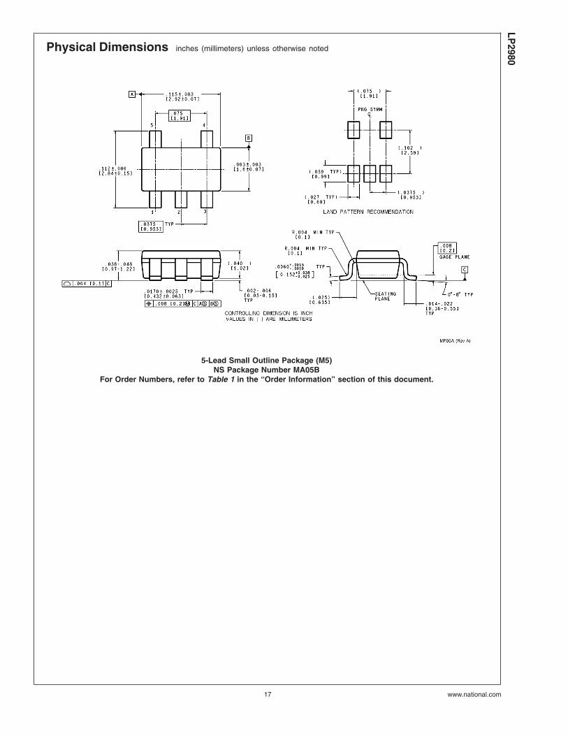
Physical Dimensions inches (millimeters) unless otherwise noted
5-Lead Small Outline Package (M5)NS Package Number MA05B
For Order Numbers, refer to Table 1 in the “Order Information” section of this document.
LP2980
www.national.com17
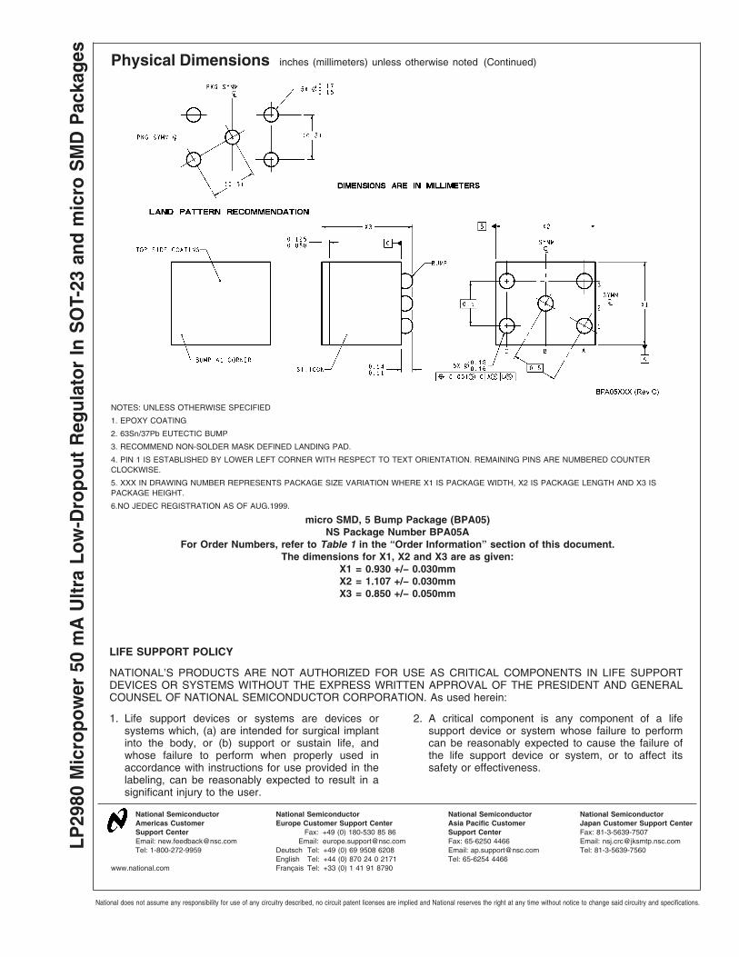
Physical Dimensions inches (millimeters) unless otherwise noted (Continued)
NOTES: UNLESS OTHERWISE SPECIFIED
1. EPOXY COATING
2. 63Sn/37Pb EUTECTIC BUMP
3. RECOMMEND NON-SOLDER MASK DEFINED LANDING PAD.
4. PIN 1 IS ESTABLISHED BY LOWER LEFT CORNER WITH RESPECT TO TEXT ORIENTATION. REMAINING PINS ARE NUMBERED COUNTERCLOCKWISE.
5. XXX IN DRAWING NUMBER REPRESENTS PACKAGE SIZE VARIATION WHERE X1 IS PACKAGE WIDTH, X2 IS PACKAGE LENGTH AND X3 ISPACKAGE HEIGHT.
6.NO JEDEC REGISTRATION AS OF AUG.1999.
micro SMD, 5 Bump Package (BPA05)NS Package Number BPA05A
For Order Numbers, refer to Table 1 in the “Order Information” section of this document.The dimensions for X1, X2 and X3 are as given:
X1 = 0.930 +/− 0.030mmX2 = 1.107 +/− 0.030mmX3 = 0.850 +/− 0.050mm
LIFE SUPPORT POLICY
NATIONAL’S PRODUCTS ARE NOT AUTHORIZED FOR USE AS CRITICAL COMPONENTS IN LIFE SUPPORTDEVICES OR SYSTEMS WITHOUT THE EXPRESS WRITTEN APPROVAL OF THE PRESIDENT AND GENERALCOUNSEL OF NATIONAL SEMICONDUCTOR CORPORATION. As used herein:
1. Life support devices or systems are devices orsystems which, (a) are intended for surgical implantinto the body, or (b) support or sustain life, andwhose failure to perform when properly used inaccordance with instructions for use provided in thelabeling, can be reasonably expected to result in asignificant injury to the user.
2. A critical component is any component of a lifesupport device or system whose failure to performcan be reasonably expected to cause the failure ofthe life support device or system, or to affect itssafety or effectiveness.
National SemiconductorAmericas CustomerSupport CenterEmail: [email protected]: 1-800-272-9959
National SemiconductorEurope Customer Support Center
Fax: +49 (0) 180-530 85 86Email: [email protected]
Deutsch Tel: +49 (0) 69 9508 6208English Tel: +44 (0) 870 24 0 2171Français Tel: +33 (0) 1 41 91 8790
National SemiconductorAsia Pacific CustomerSupport CenterFax: 65-6250 4466Email: [email protected]: 65-6254 4466
National SemiconductorJapan Customer Support CenterFax: 81-3-5639-7507Email: [email protected]: 81-3-5639-7560
www.national.com
LP29
80M
icro
pow
er50
mA
Ultr
aLo
w-D
ropo
utR
egul
ator
InS
OT-
23an
dm
icro
SM
DP
acka
ges
National does not assume any responsibility for use of any circuitry described, no circuit patent licenses are implied and National reserves the right at any time without notice to change said circuitry and specifications.