precision, micropower, low-dropout, high- output-current, so-8 voltage...
TRANSCRIPT

19-1650; Rev 0; 7/00
General DescriptionThe MAX6161–MAX6167 are precision, low-dropout,micropower voltage references. These three-terminaldevices operate with an input voltage range from (VOUT+ 200mV) to 12.6V and are available with output volt-age options of 1.25V, 2.048V, 2.5V, 3V, 4.096V, 4.5V,and 5V. They feature a proprietary curvature-correctioncircuit and laser-trimmed thin-film resistors that result ina very low temperature coefficient of 5ppm/°C (max)and an initial accuracy of ±2mV (max). Specificationsapply to the extended temperature range (-40°C to+85°C).
The MAX6161–MAX6167 typically draw only 90µA ofsupply current and can source 5mA (4mA forMAX6161) or sink 2mA of load current. Unlike conven-tional shunt-mode (two-terminal) references that wastesupply current and require an external resistor, thesedevices offer a supply current that is virtually indepen-dent of the supply voltage (8µA/V variation) and do notrequire an external resistor. Additionally, the internallycompensated devices do not require an external com-pensation capacitor and are stable with up to 1µF ofload capacitance. Eliminating the external compensa-tion capacitor saves valuable board area in space-criti-cal applications. Low dropout voltage and supplyindependent, ultra-low supply current make thesedevices ideal for battery-operated, high-performance,low-voltage systems.
The MAX6161–MAX6167 are available in 8-pin SOpackages.
________________________ApplicationsAnalog-to-Digital Converters (ADCs)
Portable Battery-Powered Systems
Notebook Computers
PDAs, GPS, DMMs
Cellular Phones
Precision 3V/5V Systems
____________________________Features ±2mV max Initial Accuracy
5ppm/°C max Temperature Coefficient
5mA Source Current at 0.9mV/mA
2mA Sink Current at 2.5mV/mA
Stable with CLOAD = 0 to 1µF
90µA typ Quiescent Supply Current
200mV max Dropout at 1mA Load Current
60µV/V Line Regulation
Output Voltage Options: 1.25V, 2.048V, 2.5V, 3V,4.096V, 4.5V, 5V
Ordering Information
MA
X6
16
1–M
AX
61
67
Precision, Micropower, Low-Dropout, High-Output-Current, SO-8 Voltage References
________________________________________________________________ Maxim Integrated Products 1
OUT
N.C.GND
1
2
8
7
N.C.
N.C.IN
N.C.
N.C.
SO
TOP VIEW
3
4
6
5
MAX6161–MAX6167
___________________Pin Configuration
For free samples and the latest literature, visit www.maxim-ic.com or phone 1-800-998-8800.For small orders, phone 1-800-835-8769.
*Insert the code for the desired initial accuracy and temperature coefficient (from the Selector Guide) in the blank to complete the part number.
Typical Operating Circuit and Selector Guide appear at endof data sheet.
PART*TEMP.RANGE
PIN-PACKAGE
OUTPUTVOLTAGE
(V)
MAX6161_ESA -40°C to +85°C 8 SO 1.250
MAX6162_ESA -40°C to +85°C 8 SO 2.048
MAX6163_ESA -40°C to +85°C 8 SO 3.000
MAX6164_ESA -40°C to +85°C 8 SO 4.096
MAX6165_ESA -40°C to +85°C 8 SO 5.000
MAX6166_ESA -40°C to +85°C 8 SO 2.500
MAX6167_ESA -40°C to +85°C 8 SO 4.500

MA
X6
16
1–M
AX
61
67
Precision, Micropower, Low-Dropout, High-Output-Current, SO-8 Voltage References
2 _______________________________________________________________________________________
ABSOLUTE MAXIMUM RATINGS
Stresses beyond those listed under “Absolute Maximum Ratings” may cause permanent damage to the device. These are stress ratings only, and functionaloperation of the device at these or any other conditions beyond those indicated in the operational sections of the specifications is not implied. Exposure toabsolute maximum rating conditions for extended periods may affect device reliability.
Voltages Referenced to GNDIN …………............................................................-0.3 to +13.5VOUT……………… ........................................-0.3V to (VIN + 0.3V)Output Short-Circuit Duration to GND or IN (VIN ≤ 6V) ...ContinuousOutput Short-Circuit Duration to GND or IN (VIN > 6V)…...........60s
Continuous Power Dissipation (TA = +70°C)8-Pin SO (derate 5.88mW/°C above +70°C)...............471mW
Operating Temperature Range ...........................-40°C to +85°CStorage Temperature Range………….…………-65°C to +150°CLead Temperature (soldering, 10s)……………………….+300°C
ELECTRICAL CHARACTERISTICS—MAX6161 (VOUT = 1.25V)(VIN = 5V, IOUT = 0, TA = TMIN to TMAX, unless otherwise specified. Typical values are at TA = +25°C.)
PARAMETER SYMBOL CONDITIONS MIN TYP MAX UNITS
MAX6161A 1.248 1.250 1.252Output Voltage VOUT TA = +25°C
MAX6161B 1.246 1.250 1.254V
MAX6161A 2 5Output Voltage TemperatureCoefficient (Note 1)
TCVOUTMAX6161B 4 10
ppm/°C
Line Regulation∆VOUT/
∆VIN2.5V < VIN < 12.6V 6 60 µV/V
Sourcing: 0 < IOUT < 4mA 0.5 0.9Load Regulation
∆VOUT/∆IOUT Sinking: -2mA < IOUT < 0 1.3 2.5
mV/mA
Short to GND 25OUT Short-Circuit Current ISC
Short to IN 25mA
Long-Term Stability∆VOUT/
time1000hr at +25°C 80
ppm/1000hr
Output Voltage Hysteresis(Note 2)
∆VOUT/cycle
80 ppm
DYNAMIC CHARACTERISTICS
f = 0.1Hz to 10Hz 20 µVp-pNoise Voltage eOUT
f = 10Hz to 10kHz 15 µVRMS
Ripple Rejection VOUT/VIN VIN = 5V ±100mV, f = 120Hz 80 dB
Turn-On Settling Time tR VOUT to 0.1% of final value, COUT = 50pF 50 µs
Capacitive-Load Stability Range(Note 3)
COUT 0 1.0 µF
INPUT CHARACTERISTICS
Supply Voltage Range VIN Guaranteed by line-regulation test VOUT + 0.2 12.6 V
Quiescent Supply Current IIN 90 120 µA
Change in Supply Current ∆IIN/∆VIN 2.5V < VIN < 12.6V 3.2 8.0 µA/V

MA
X6
16
1–M
AX
61
67
Precision, Micropower, Low-Dropout, High-Output-Current, SO-8 Voltage References
_______________________________________________________________________________________ 3
ELECTRICAL CHARACTERISTICS—MAX6162 (VOUT = 2.048V)(VIN = 5V, IOUT = 0, TA = TMIN to TMAX, unless otherwise specified. Typical values are at TA = +25°C.)
PARAMETER SYMBOL CONDITIONS MIN TYP MAX UNITS
MAX6162A 2.046 2.048 2.050Output Voltage VOUT TA = +25°C
MAX6162B 2.043 2.048 2.053V
MAX6162A 2 5Output Voltage TemperatureCoefficient (Note 1)
TCVOUTMAX6162B 4 10
ppm/°C
Line Regulation ∆VOUT/ 2.5V < VIN < 12.6V 42 130 µV/V
Sourcing: 0 < IOUT < 5mA 0.5 0.9Load Regulation
∆VOUT/∆IOUT Sinking: -2mA < IOUT < 0 1.5 4
mV/mA
Short to GND 25OUT Short-Circuit Current ISC
Short to IN 25mA
Long-Term Stability∆VOUT/
time1000hr at +25°C 80
ppm/1000hr
Output Voltage Hysteresis(Note 2)
∆VOUT/cycle
80 ppm
DYNAMIC CHARACTERISTICS
f = 0.1Hz to 10Hz 22 µVp-pNoise Voltage eOUT
f = 10Hz to 10kHz 22 µVRM S
Ripple Rejection VOUT/VIN VIN = 5V ±100mV, f = 120Hz 78 dB
Turn-On Settling Time tR VOUT to 0.1% of final value, COUT = 50pF 100 µs
Capacitive-Load Stability Range(Note 3)
COUT 0 1.0 µF
INPUT CHARACTERISTICS
Supply Voltage Range VIN Guaranteed by line-regulation test VOUT + 0.2 12.6 V
Quiescent Supply Current IIN 90 120 µA
Change in Supply Current ∆IIN/∆VIN 2.5V < VIN < 12.6V 3.4 8.0 µA/V
MA
X6
16
1–M
AX
61
67
Precision, Micropower, Low-Dropout, High-Output-Current, SO-8 Voltage References
4 _______________________________________________________________________________________
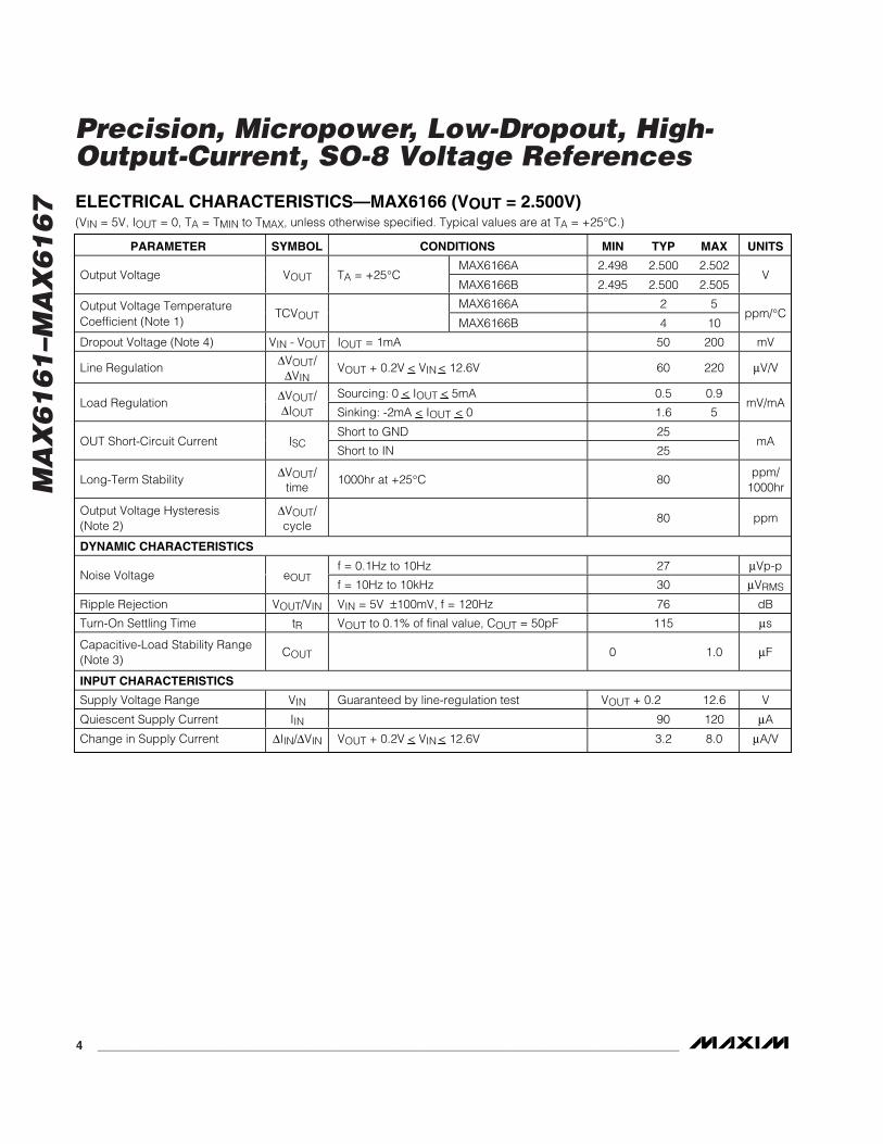
ELECTRICAL CHARACTERISTICS—MAX6166 (VOUT = 2.500V)(VIN = 5V, IOUT = 0, TA = TMIN to TMAX, unless otherwise specified. Typical values are at TA = +25°C.)
PARAMETER SYMBOL CONDITIONS MIN TYP MAX UNITS
MAX6166A 2.498 2.500 2.502Output Voltage VOUT TA = +25°C
MAX6166B 2.495 2.500 2.505V
MAX6166A 2 5Output Voltage TemperatureCoefficient (Note 1)
TCVOUTMAX6166B 4 10
ppm/°C
Dropout Voltage (Note 4) VIN - VOUT IOUT = 1mA 50 200 mV
Line Regulation∆VOUT/
∆VINVOUT + 0.2V < VIN < 12.6V 60 220 µV/V
Sourcing: 0 < IOUT < 5mA 0.5 0.9Load Regulation
∆VOUT/∆IOUT Sinking: -2mA < IOUT < 0 1.6 5
mV/mA
Short to GND 25OUT Short-Circuit Current ISC
Short to IN 25mA
Long-Term Stability∆VOUT/
time1000hr at +25°C 80
ppm/1000hr
Output Voltage Hysteresis(Note 2)
∆VOUT/cycle
80 ppm
DYNAMIC CHARACTERISTICS
f = 0.1Hz to 10Hz 27 µVp-pNoise Voltage eOUT
f = 10Hz to 10kHz 30 µVRMS
Ripple Rejection VOUT/VIN VIN = 5V ±100mV, f = 120Hz 76 dB
Turn-On Settling Time tR VOUT to 0.1% of final value, COUT = 50pF 115 µs
Capacitive-Load Stability Range(Note 3)
COUT 0 1.0 µF
INPUT CHARACTERISTICS
Supply Voltage Range VIN Guaranteed by line-regulation test VOUT + 0.2 12.6 V
Quiescent Supply Current IIN 90 120 µA
Change in Supply Current ∆IIN/∆VIN VOUT + 0.2V < VIN < 12.6V 3.2 8.0 µA/V

MA
X6
16
1–M
AX
61
67
Precision, Micropower, Low-Dropout, High-Output-Current, SO-8 Voltage References
_______________________________________________________________________________________ 5
ELECTRICAL CHARACTERISTICS—MAX6163 (VOUT = 3.000V)(VIN = 5V, IOUT = 0, TA = TMIN to TMAX, unless otherwise specified. Typical values are at TA = +25°C.)
PARAMETER SYMBOL CONDITIONS MIN TYP MAX UNITS
MAX6163A 2.998 3.000 3.002Output Voltage VOUT TA = +25°C
MAX6163B 2.995 3.000 3.005V
MAX6163A 2 5Output Voltage TemperatureCoefficient (Note 1)
TCVOUT -40°C to +85°CMAX6163B 4 10
ppm/°C
Dropout Voltage (Note 4) VIN - VOUT IOUT = 1mA 50 200 mV
Line Regulation∆VOUT/
∆VINVOUT + 0.2V < VIN < 12.6V 83 300 µV/V
Sourcing: 0 < IOUT < 5mA 0.5 0.9Load Regulation
∆VOUT/∆IOUT Sinking: -2mA < IOUT < 0 1.8 5
mV/mA
Short to GND 25OUT Short-Circuit Current ISC
Short to IN 25mA
Long-Term Stability∆VOUT/
time1000hr at +25°C 80
ppm/1000hr
Output Voltage Hysteresis(Note 2)
∆VOUT/cycle
80 ppm
DYNAMIC CHARACTERISTICS
f = 0.1Hz to 10Hz 35 µVp-pNoise Voltage eOUT
f = 10Hz to 10kHz 40 µVRMS
Ripple Rejection VOUT/VIN VIN = 5V ±100mV, f = 120Hz 76 dB
Turn-On Settling Time tR VOUT to 0.1% of final value, COUT = 50pF 115 µs
Capacitive-Load Stability Range(Note 3)
COUT 0 1.0 µF
INPUT CHARACTERISTICS
Supply Voltage Range VIN Guaranteed by line-regulation test VOUT + 0.2 12.6 V
Quiescent Supply Current IIN 90 120 µA
Change in Supply Current ∆IIN/∆VIN VOUT + 0.2V < VIN < 12.6V 3.2 8.0 µA/V

MA
X6
16
1–M
AX
61
67
Precision, Micropower, Low-Dropout, High-Output-Current, SO-8 Voltage References
6 _______________________________________________________________________________________
ELECTRICAL CHARACTERISTICS—MAX6164 (VOUT = 4.096V)(VIN = 5V, IOUT = 0, TA = TMIN to TMAX, unless otherwise specified. Typical values are at TA = +25°C.)
PARAMETER SYMBOL CONDITIONS MIN TYP MAX UNITS
MAX6164A 4.094 4.096 4.098Output Voltage VOUT TA = +25°C
MAX6164B 4.091 4.096 4.101V
MAX6164A 2 5Output Voltage TemperatureCoefficient (Note 1)
TCVOUTMAX6164B 4 10
ppm/°C
Dropout Voltage (Note 4) VIN - VOUT IOUT = 1mA 50 200 mV
Line Regulation∆VOUT/
∆VINVOUT + 0.2V < VIN < 12.6V 140 300 µV/V
Sourcing: 0 < IOUT < 5mA 0.6 0.9Load Regulation
∆VOUT/∆IOUT Sinking: -2mA < IOUT < 0 2.0 7.0
mV/mA
Short to GND 25OUT Short-Circuit Current ISC
Short to IN 25mA
Long-Term Stability∆VOUT/
time1000hr at +25°C 80
ppm/1000hr
Output Voltage Hysteresis(Note 2)
∆VOUT/cycle
80 ppm
DYNAMIC CHARACTERISTICS
f = 0.1Hz to 10Hz 50 µVp-pNoise Voltage eOUT
f = 10Hz to 10kHz 50 µVRMS
Ripple Rejection VOUT/VIN VIN = 5V ±100mV, f = 120Hz 72 dB
Turn-On Settling Time tR VOUT to 0.1% of final value, COUT = 50pF 190 µs
Capacitive-Load Stability Range(Note 3)
COUT 0 1.0 µF
INPUT CHARACTERISTICS
Supply Voltage Range VIN Guaranteed by line-regulation test VOUT + 0.2 12.6 V
Quiescent Supply Current IIN 90 120 µA
Change in Supply Current ∆IIN/∆VIN VOUT + 0.2V < VIN < 12.6V 3.2 8.0 µA/V

MA
X6
16
1–M
AX
61
67
Precision, Micropower, Low-Dropout, High-Output-Current, SO-8 Voltage References
_______________________________________________________________________________________ 7
ELECTRICAL CHARACTERISTICS—MAX6167 (VOUT = 4.500V)(VIN = 5V, IOUT = 0, TA = TMIN to TMAX, unless otherwise specified. Typical values are at TA = +25°C.)
PARAMETER SYMBOL CONDITIONS MIN TYP MAX UNITS
MAX6167A 4.498 4.500 4.502Output Voltage VOUT TA = +25°C
MAX6167B 4.495 4.500 4.505V
MAX6167A 2 5Output Voltage TemperatureCoefficient (Note 1)
TCVOUTMAX6167B 4 10
ppm/°C
Dropout Voltage (Note 4) VIN - VOUT IOUT = 1mA 50 200 mV
Line Regulation∆VOUT/
∆VINVOUT + 0.2V < VIN < 12.6V 160 450 µV/V
Sourcing: 0 < IOUT < 5mA 0.6 0.9Load Regulation
∆VOUT/∆IOUT Sinking: -2mA < IOUT < 0 2.3 8.0
mV/mA
Short to GND 25OUT Short-Circuit Current ISC
Short to IN 25mA
Long-Term Stability∆VOUT/
time1000hr at +25°C 80
ppm/1000hr
Output Voltage Hysteresis(Note 2)
∆VOUT/cycle
80 ppm
DYNAMIC CHARACTERISTICS
f = 0.1Hz to 10Hz 55 µVp-pNoise Voltage eOUT
f = 10Hz to 10kHz 55 µVRMS
Ripple Rejection VOUT/VIN VIN = 5V ±100mV, f = 120Hz 70 dB
Turn-On Settling Time tR VOUT to 0.1% of final value, COUT = 50pF 230 µs
Capacitive-Load Stability Range(Note 3)
COUT 0 1.0 µF
INPUT CHARACTERISTICS
Supply Voltage Range VIN Guaranteed by line-regulation test VOUT + 0.2 12.6 V
Quiescent Supply Current IIN 90 120 µA
Change in Supply Current ∆IIN/∆VIN VOUT + 0.2V < VIN < 12.6V 3.1 8.0 µA/V

MA
X6
16
1–M
AX
61
67
Precision, Micropower, Low-Dropout, High-Output-Current, SO-8 Voltage References
8 _______________________________________________________________________________________
ELECTRICAL CHARACTERISTICS—MAX6165 (VOUT = 5.000V)(VIN = 5V, IOUT = 0, TA = TMIN to TMAX, unless otherwise specified. Typical values are at TA = +25°C.)
PARAMETER SYMBOL CONDITIONS MIN TYP MAX UNITS
MAX6165A 4.998 5.000 5.002Output Voltage VOUT TA = +25°C
MAX6165B 4.995 5.000 5.005V
MAX6165A 2 5Output Voltage TemperatureCoefficient (Note 1)
TCVOUTMAX6165B 4 10
ppm/°C
Dropout Voltage (Note 4) VIN - VOUT IOUT = 1mA 50 200 mV
Line Regulation ∆VOUT/ VOUT + 0.2V < VIN < 12.6V 180 400 µV/V
Sourcing: 0 < IOUT < 5mA 0.6 0.9Load Regulation
∆VOUT/∆IOUT Sinking: -2mA < IOUT < 0 2.4 8.0
mV/mA
Short to GND 25OUT Short-Circuit Current ISC
Short to IN 25mA
Long-Term Stability∆VOUT/
time1000hr at +25°C 80
ppm/1000hr
Output Voltage Hysteresis(Note 2)
∆VOUT/cycle
80 ppm
DYNAMIC CHARACTERISTICS
f = 0.1Hz to 10Hz 60 µVp-pNoise Voltage eOUT
f = 10Hz to 10kHz 60 µVRMS
Ripple Rejection VOUT/VIN VIN = 5V ± 100mV, f = 120Hz 65 dB
Turn-On Settling Time tR VOUT to 0.1% of final value, COUT = 50pF 300 µs
Capacitive-Load Stability Range(Note 3)
COUT 0 1.0 µF
INPUT CHARACTERISTICS
Supply Voltage Range VIN Guaranteed by line-regulation test VOUT + 0.2 12.6 V
Quiescent Supply Current IIN 90 120 µA
Change in Supply Current ∆IIN/∆VIN VOUT + 0.2V < VIN < 12.6V 3.1 8.0 µA/V
Note 1: Temperature Coefficient is specified by the “box” method; i.e., the maximum ∆VOUT is divided by the maximum ∆T.Note 2: Thermal Hysteresis is defined as the change in TA = +25°C output voltage before and after temperature cycling of the
device (from TA = TMIN to TMAX). Initial measurement at TA = +25°C is followed by temperature cycling the device to TA = +85°C then to TA = -40°C, and another measurement at TA = +25°C is compared to the original measurement at TA = +25°C.
Note 3: Not production tested. Guaranteed by design.Note 4: Dropout voltage is the minimum input voltage at which VOUT changes ≤ 0.2% from VOUT at VIN = 5.0V (VIN = 5.5V for
MAX6165).

MA
X6
16
1–M
AX
61
67
Precision, Micropower, Low-Dropout, High-Output-Current, SO-8 Voltage References
_______________________________________________________________________________________ 9
Typical Operating Characteristics
2.049
2.048
2.047-40 10-15 35 60 65
MAX6162OUTPUT VOLTAGE TEMPERATURE DRIFT
MAX
6161
/67
toc0
1
TEMPERATURE (°C)
OUTP
UT V
OLTA
GE (V
)
THREETYPICAL PARTS
4.998
4.999
5.001
5.000
5.002
5.003
-40 10-15 35 60 85
MAX6165OUTPUT VOLTAGE TEMPERATURE DRIFT
MAX
6161
/67
toc0
2
TEMPERATURE (°C)
OUTP
UT V
OLTA
GE (V
)
THREETYPICAL PARTS
0
10
5
20
15
30
25
35
0 400 600 800200 1000
MAX6161PPM vs. TIME
MAX
6161
/67
toc0
3
TIME (hr)
PPM
0
10
70
30
20
40
50
60
80
0 200 400 600 800 1000
MAX6165PPM vs. TIME
MAX
6161
/67
toc0
4
TIME (hr)
PPM
-300
-200
-100
0
100
200
300
2 4 6 8 10 12
MAX6161LINE REGULATION
MAX
6161
/67
toc0
5
INPUT VOLTAGE (V)
OUTP
UT V
OLTA
GE C
HANG
E (µ
V)
TA = +85°C
TA = +25°C
TA = -40°C
-1200
-600
-800
-1000
-400
-200
0
200
5 97 11 13
MAX6165LINE REGULATION
MAX
6161
/67
toc0
6
INPUT VOLTAGE (V)
OUTP
UT V
OLTA
GE C
HANG
E (µ
V)
TA = +85°C
TA = +25°C
TA = -40°C
-3
1
0
-1
-2
2
3
4
5
-4 -2 0 2 4
MAX
6161
/67
toc0
7
LOAD CURRENT (mA)
OUTP
UT V
OLTA
GE C
HANG
E (m
V)
TA = +25°CTA = -40°C
MAX6161LOAD REGULATION
TA = +85°C
-6
2
0
-2
-4
4
8
6
10
12
-6 -2-4 0 2 4 6
MAX
6161
/67
toc0
8
LOAD CURRENT (mA)
OUTP
UT V
OLTA
GE C
HANG
E (m
V)
MAX6165LOAD REGULATION
TA = +25°C
TA = +85°C
TA = -40°C
0
0.10
0.05
0.20
0.15
0.25
0.30
0 21 3 4 5
MAX6166DROPOUT VOLTAGEvs. LOAD CURRENT
MAX
6161
/67
toc0
9
LOAD CURRENT (mA)
DROP
OUT
VOLT
AGE
(V)
TA = +85°C
TA = +25°C
TA = -40°C
(VIN = +5V for MAX6161/2/3/4/6/7, VIN = +5.5V for MAX6165, IOUT = 0, TA = +25°C, unless otherwise noted.) (Note 5)

MA
X6
16
1–M
AX
61
67
Precision, Micropower, Low-Dropout, High-Output-Current, SO-8 Voltage References
10 ______________________________________________________________________________________
Typical Operating Characteristics (continued)
0
0.05
0.15
0.10
0.20
0.25
0 21 3 4 5
TA = +85°C
TA = +25°CTA = -40°C
MAX
6161
/67
toc1
0
LOAD CURRENT (mA)
DROP
OUT
VOLT
AGE
(V)
MAX6165DROPOUT VOLTAGEvs. LOAD CURRENT
MAX
6161
/67
toc1
1
FREQUENCY (kHz)
PSRR
(dB)
0
-10
-20
-30
-40
-50
-60
-70
-80
-900.001 1 10 1000.01 0.1 1000
MAX6161POWER-SUPPLY REJECTION RATIO
vs. FREQUENCY
-70
-800.001 10 1000
-60
-50
-40
-30
-20
-10
0
FREQUENCY (kHz)
PSRR
(dB)
0.1
MAX6165POWER-SUPPLY REJECTION RATIO
vs. FREQUENCY
MAX
6161
/67
toc1
2
70
80
90
100
110
2 4 6 8 10 12
MAX
6161
/67
toc1
3
INPUT VOLTAGE (V)
SUPP
LY C
URRE
NT (µ
A)
MAX6161SUPPLY CURRENT
vs. INPUT VOLTAGE
80
85
95
90
105
110
100
115
5 7 9 11 13
MAX
6161
/67
toc1
4
INPUT VOLTAGE (V)
SUPP
LY C
URRE
NT (µ
A)
MAX6165SUPPLY CURRENT
vs. INPUT VOLTAGE
70
80
90
100
110
120
-40 10-15 35 60 85
MAX
6161
/67
toc1
5
TEMPERATURE (°C)
SUPP
LY C
URRE
NT (µ
A)
MAX6161SUPPLY CURRENTvs. TEMPERATURE
VIN = 12.5V
VIN = 7.5V
VIN = 2.5V VIN = 5.5V
85
95
105
115
-40 10-15 35 60 85
MAX
6161
/67
toc1
6
TEMPERATURE (°C)
SUPP
LY C
URRE
NT (µ
A)
MAX6165SUPPLY CURRENTvs. TEMPERATURE
VIN = 12.5V
VIN = 7.5V
VIN = 5.5V
00.001 10 1000
40
20
60
80100
140
120
160
180
200
220
MAX
6161
/67
toc1
7
FREQUENCY (kHz)
OUTP
UT IM
PEDA
NCE
(Ω)
0.1
MAX6161OUTPUT IMPEDANCE
vs. FREQUENCY180
00.001 10 1000
40
20
60
100
80
120
140
160
MAX
6161
/67
toc1
8
FREQUENCY (kHz)
OUTP
UT IM
PEDA
NCE
(Ω)
0.1
MAX6165OUTPUT IMPEDANCE
vs. FREQUENCY
(VIN = +5V for MAX6161/2/3/4/6/7, VIN = +5.5V for MAX6165, IOUT = 0, TA = +25°C, unless otherwise noted.) (Note 5)

MA
X6
16
1–M
AX
61
67
Precision, Micropower, Low-Dropout, High-Output-Current, SO-8 Voltage References
______________________________________________________________________________________ 11
Typical Operating Characteristics (continued)
VOUT10µV/div
TIME (1s/div)
MAX61610.1Hz TO 10Hz OUTPUT NOISE
MAX
6161
/67
toc1
9
VOUT10µV/div
TIME (1s/div)
MAX6165NOISE
MAX
6161
/67
toc2
0
VOUT500mV/div
VIN5V/div
TIME (10µs/div)
MAX6161TURN-ON TRANSIENT
(CL = 50pF)
MAX
6161
/67
toc2
1
VOUT2V/div
VIN5V/div
TIME (40µs/div)
MAX6165TURN-ON TRANSIENT
(CL = 50pF)
MAX
6161
/67
toc2
2
(VIN = +5V for MAX6161/2/3/4/6/7, VIN = +5.5V for MAX6165, IOUT = 0, TA = +25°C, unless otherwise noted.) (Note 5)
IOUT500µA/div
VOUTAC-COUPLED
100mV/div
TIME (400µs/div)
MAX6161LOAD TRANSIENT
(IOUT = ±250µA, VIN = 5.0, CL = 0µF)
I OUT
+250
µAI O
UT-2
50µA
MAX6161/67 toc23
IOUT500µA/div
VOUTAC-COUPLED
50mV/div
TIME (400µs/div)
MAX6165LOAD TRANSIENT
(IOUT = ±250µA, CL = 0µF, VIN = 5.5V)
+250
µA-2
50µA
MAX6161/67 toc24
IOUT500µA/div
VOUTAC-COUPLED
10mV/div
TIME (400µs/div)
MAX6161LOAD TRANSIENT
(IOUT = ±250µA, VIN = 5.0V, CL = 1µF)
+250µA
-250µA
MAX6161/67 toc25
IOUT500µA/div
VOUTAC-COUPLED
20mV/div
TIME (400µs/div)
MAX6165LOAD TRANSIENT
(IOUT = ±250µA, CL = 1µF, VIN = 5.5V)
+250µA
-250µA
MAX6161/67 toc26

MA
X6
16
1–M
AX
61
67
Precision, Micropower, Low-Dropout, High-Output-Current, SO-8 Voltage References
12 ______________________________________________________________________________________
IOUT5mA/div
VOUTAC-COUPLED
200mV/div
TIME (400µs/div)
MAX6161LOAD TRANSIENT
(VIN = 5.0V, CL = 0µF, IOUT = ±4mA)
+4mA
-4mA
MAX6161/67 toc31
IOUT5mA/div
VOUTAC-COUPLED
100mV/div
TIME (400µs/div)
MAX6165LOAD TRANSIENT
(IOUT = ±5mA, CL = 0µF, VIN = 5.5V)
+5mA
-5mA
MAX6161/67 toc32
Typical Operating Characteristics (continued)
IOUT5mA/div
VOUTAC-COUPLED
50mV/div
TIME (400µs/div)
MAX6165LOAD TRANSIENT
(CL = 0µF, IOUT = ±2mA, VIN = 5.5V)
+2mA
-2mA
MAX6161/67 toc28
IOUT5mA/div
VOUTAC-COUPLED
100mV/div
TIME (400µs/div)
MAX6161LOAD TRANSIENT
(VIN = 5.0V, CL = 0µF, IOUT = ±2mA)
+2mA
-2mA
MAX6161/67 toc27
(VIN = +5V for MAX6161/2/3/4/6/7, VIN = +5.5V for MAX6165, IOUT = 0, TA = +25°C, unless otherwise noted.) (Note 5)
IOUT5mA/div
VOUTAC-COUPLED
50mV/div
TIME (400µs/div)
MAX6161LOAD TRANSIENT
(VIN = 5.0V, CL = 1µF, IOUT = ±2mA)
+2mA
-2mA
MAX6161/67 toc29
IOUT5mA/div
VOUTAC-COUPLED
20mV/div
TIME (400µs/div)
MAX6165LOAD TRANSIENT
(CL = 1µF, IOUT = ±2mA, VIN = 5.5V)
+2mA
-2mA
MAX6161/67 toc30

MA
X6
16
1–M
AX
61
67
Precision, Micropower, Low-Dropout, High-Output-Current, SO-8 Voltage References
______________________________________________________________________________________ 13
Typical Operating Characteristics (continued)
IOUT5mA/div
VOUTAC-COUPLED
50mV/div
TIME (400µs/div)
MAX6161LOAD TRANSIENT
(VIN = 5.0V, CL = 1µF, IOUT = ±4mA)
+4mA
-4mA
MAX6161/67 toc33
IOUT5mA/div
VOUTAC-COUPLED
50mV/div
TIME (400µs/div)
MAX6165LOAD TRANSIENT
(IOUT = ±5mA, CL = 1µF, VIN = 5.5V)
+5mA
-5mA
MAX6161/67 toc34
(VIN = +5V for MAX6161/2/3/4/6/7, VIN = +5.5V for MAX6165, IOUT = 0, TA = +25°C, unless otherwise noted.) (Note 5)
Pin Description
GroundGND4
Reference OutputOUT6
PINMAX617_
Input VoltageIN2
No Connection. Not internally connected.N.C.1, 3, 5, 7, 8
FUNCTIONNAME
VIN500mV/div
VOUTAC-COUPLED
20mV/div
TIME (40µs/div)
MAX6161LINE TRANSIENT
(CL = 0)
+0.25
-0.25
MAX6161/67 toc35
VIN500mV/div
VOUTAC-COUPLED
20mV/div
TIME (40µs/div)
MAX6165LINE TRANSIENT
(CL = 0)
+0.25
-0.25
MAX6161/67 toc36
Note 5: Many of the MAX6161 family Typical Operating Characteristics are extremely similar. The extremes of these characteristicsare found in the MAX6161 (1.25V output) and the MAX6165 (5.0V output). The Typical Operating Characteristics of theremainder of the MAX6161 family typically lie between these two extremes and can be estimated based on their output voltages.

Applications InformationInput Bypassing
For the best line-transient performance, decouple theinput with a 0.1µF ceramic capacitor as shown in theTypical Operating Circuit. Locate the capacitor asclose to IN as possible. When transient performance isless important, no capacitor is necessary.
Output/Load CapacitanceDevices in the MAX6161 family do not require an outputcapacitor for frequency stability. They are stable forcapacitive loads from 0 to 1µF. However, in applica-tions where the load or the supply can experience stepchanges, an output capacitor will reduce the amount ofovershoot (undershoot) and improve the circuit’s tran-sient response. Many applications do not require anexternal capacitor, and the MAX6161 family can offer asignificant advantage in applications when boardspace is critical.
Supply CurrentThe quiescent supply current of the series-modeMAX6161 family is typically 90µA and is virtually inde-pendent of the supply voltage, with only a 8µA/V (max)variation with supply voltage. Unlike series references,shunt-mode references operate with a series resistorconnected to the power supply. The quiescent currentof a shunt-mode reference is thus a function of theinput voltage. Additionally, shunt-mode referenceshave to be biased at the maximum expected load cur-rent, even if the load current is not present at the time.In the MAX6161 family, the load current is drawn fromthe input voltage only when required, so supply currentis not wasted and efficiency is maximized at all inputvoltages. This improved efficiency reduces power dissi-pation and extends battery life.
When the supply voltage is below the minimum speci-fied input voltage (as during turn-on), the devices candraw up to 400µA beyond the nominal supply current.The input voltage source must be capable of providingthis current to ensure reliable turn-on.
Output Voltage HysteresisOutput voltage hysteresis is the change in the inputvoltage at TA = +25°C before and after the device iscycled over its entire operating temperature range.Hysteresis is caused by differential package stressappearing across the bandgap core transistors. Thetypical temperature hysteresis value is 80ppm.
Turn-On TimeThese devices typically turn on and settle to within0.1% of their final value in 50µs to 300µs, depending on
the output voltage (see electrical table of part used).The turn-on time can increase up to 1.5ms with thedevice operating at the minimum dropout voltage andthe maximum load.
Positive and Negative Low-Power Voltage Reference
Figure 1 shows a typical method for developing a bipo-lar reference. The circuit uses a MAX681 voltage dou-bler/inverter charge-pump converter to power anICL7652, thus creating a positive as well as a negativereference voltage.
MA
X6
16
1–M
AX
61
67
Precision, Micropower, Low-Dropout, High-Output-Current, SO-8 Voltage References
14 ______________________________________________________________________________________
IN
VS
+2VS
-2VS
OUT +REF OUTPUT
OUTPUT
-REF OUTPUT
10nF1M, 0.1%
1M, 0.1%
GND
MAX6161MAX6167
VCC V+
GNDMAX681
V-
V+
V-
ICL7652
Figure 1. Positive and Negative References from Single +3V or+5V Supply
IN
+SUPPLY INPUT (SEE SELECTOR GUIDE)
OUT REFERENCE OUT
1µF MAX*
*CAPACITORS ARE OPTIONAL.
GND
MAX6161–MAX61670.1µF*
__________ Typical Operating Circuit
__________________________Chip TopographyTRANSISTOR COUNT:117
PROCESS: BiCMOS

MA
X6
16
1–M
AX
61
67
Precision, Micropower, Low-Dropout, High-Output-Current, SO-8 Voltage References
______________________________________________________________________________________ 15
Selector Guide
PART OUTPUT VOLTAGE
(V)
INITIAL ACCURACY
(mV)
TEMPERATURECOEFFICIENT
(ppm/°C)
MAX6161A 1.250 ±2 5
MAX6161B 1.250 ±4 10
MAX6162A 2.048 ±2 5
MAX6162B 2.048 ±5 10
MAX6166A 2.500 ±2 5
MAX6166B 2.500 ±5 10
MAX6163A 3.000 ±2 5
MAX6163B 3.000 ±5 10
MAX6164A 4.096 ±2 5
MAX6164B 4.096 ±5 10
MAX6167A 4.500 ±2 5
MAX6167B 4.500 ±5 10
MAX6165A 5.000 ±2 5
MAX6165B 5.000 ±5 10

MA
X6
16
1–M
AX
61
67
Precision, Micropower, Low-Dropout, High-Output-Current, SO-8 Voltage References
Maxim cannot assume responsibility for use of any circuitry other than circuitry entirely embodied in a Maxim product. No circuit patent licenses areimplied. Maxim reserves the right to change the circuitry and specifications without notice at any time.
16 ____________________Maxim Integrated Products, 120 San Gabriel Drive, Sunnyvale, CA 94086 408-737-7600
© 2000 Maxim Integrated Products Printed USA is a registered trademark of Maxim Integrated Products.
Package Information
SO
ICN
.EP
S